

1 MSPS, 12-Bit, Simultaneous Sampling
V
A
SAR ADC with PGA and Four Comparators
FEATURES
Dual simultaneous sampling 12-bit, 2-channel ADC
True differential analog inputs
Programmable gain stage: ×1, ×2, ×3, ×4, ×6, ×8, ×12, ×16,
×24, ×32, ×48, ×64, ×96, ×128
Throughput rate per ADC
1 MSPS for AD7262
500 kSPS for AD7262-5
Analog input impedance: >1 GΩ
Wide input bandwidth
−3 dB bandwidth: 1.7 MHz at gain = 2
4 on-chip comparators
SNR: 73 dB typical at gain = 2, 66 dB typical at gain = 32
Device offset calibration, system gain calibration
On-chip reference: 2.5 V
–40°C to +105°C operation
High speed serial interface
SPI/QSPI™/MICROWIRE™/DSP compatible
48-lead LFCSP and LQFP packages
GENERAL DESCRIPTION
The AD7262/AD7262-5 are dual, 12-bit, high speed, low power,
successive approximation ADCs that operate from a single 5 V
power supply. The AD7262 features throughput rates of up to
1 MSPS per on-chip ADC. The AD7262-5 features throughput
rates of up to 500 kSPS. Two complete ADC functions allow
simultaneous sampling and conversion of two channels. Each
ADC is preceded by a true differential analog input with a PGA.
There are 14 gain settings available: ×1, ×2, ×3, ×4, ×6, ×8, ×12,
×16, ×24, ×32, ×48, ×64, ×96, and ×128.
The AD7262/AD7262-5 contain four comparators. Comparator A
and Comparator B are optimized for low power, while Comparator C and Comparator D have fast propagation delays. The
AD7262/AD7262-5 feature a calibration function to remove any
device offset error and programmable gain adjust registers to
allow for input path (for example, sensor) offset and gain
compensation. The AD7262/AD7262-5 have an on-chip 2.5 V
reference that can be disabled if an external reference is preferred.
The AD7262/AD7262-5 are ideally suited for monitoring small
amplitude signals from a variety of sensors. They include all the
functionality needed for monitoring the position feedback
signals from a variety of analog encoders used in motor control
systems.
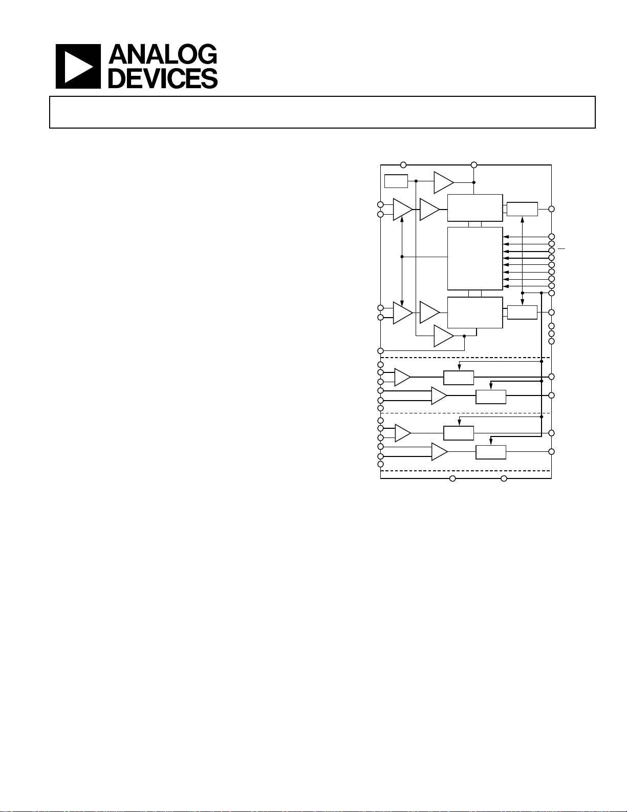
AD7262
FUNCTIONAL BLOCK DIAGRAM
V
CC
VA+
V
V
V
V
REF
C
A_CBVCC
C
C
C
C
CA_CB_GND
C
C_CDVCC
C
C
C
C
CC_CD_GND
A
B
B
B
A
A
B
B
C
C
D
D
–
+
–
+
–
+
–
+
–
+
–
REF
PGA T/H
PGA
COMP
COMP
BUF
T/H
BUF
OUTPUT
DRIVERS
COMP
OUTPUT
DRIVERS
COMP
AGND DGND
PRODUCT HIGHLIGHTS
1. Integrated PGA with a variety of flexible gain settings to
allow detection and conversion of low level analog signals.
2. Each PGA is followed by a dual simultaneous sampling
ADC, featuring throughput rates of 1 MSPS per ADC for
the AD7262. The conversion results of both ADCs are
simultaneously available on separate data lines or in succession on one data line if only one serial port is available.
3. Four integrated comparators that can be used to count
signals from pole sensors in motor control applications.
4. Internal 2.5 V reference.
A
REF
12-BIT
SUCCESSIVE
APPROXIMATION
ADC
CONTRO L
LOGIC
12-BIT
SUCCESSIVE
APPROXIMATION
ADC
OUTPUT
DRIVERS
OUTPUT
DRIVERS
Figure 1.
AD7262
OUTPUT
DRIVERS
OUTPUT
DRIVERS
D
OUT
SCLK
CAL
CS
REFSEL
G0
G1
G2
G3
V
DRIVE
D
OUT
PD0/D
PD1
PD2
C
OUT
C
OUT
C
OUT
C
OUT
A
B
IN
A
B
C
D
07606-001
Rev. 0
Information furnished by Analog Devices is believed to be accurate and reliable. However, no
responsibility is assumed by Analog Devices for its use, nor for any infringements of patents or other
rights of third parties that may result from its use. Specifications subject to change without notice. No
license is granted by implication or otherwise under any patent or patent rights of Analog Devices.
Trademarks and registered trademarks are the property of their respective owners.
One Technology Way, P.O. Box 9106, Norwood, MA 02062-9106, U.S.A.
Tel: 781.329.4700 www.analog.com
Fax: 781.461.3113 ©2008 Analog Devices, Inc. All rights reserved.

AD7262
TABLE OF CONTENTS
Features .............................................................................................. 1
General Description ......................................................................... 1
Functional Block Diagram .............................................................. 1
Product Highlights ........................................................................... 1
Revision History ............................................................................... 2
Specifications ..................................................................................... 3
Timing Specifications .................................................................. 6
Timing Diagram ........................................................................... 6
Absolute Maximum Ratings ............................................................ 7
ESD Caution .................................................................................. 7
Pin Configurations and Function Descriptions ........................... 8
Typical Performance Characteristics ........................................... 10
Terminology .................................................................................... 14
Theory of Operation ...................................................................... 15
Circuit Information .................................................................... 15
Comparators ................................................................................ 15
Operation ..................................................................................... 15
Analog Inputs .............................................................................. 15
V
............................................................................................ 16
DRIVE
Reference ..................................................................................... 17
Typical Connection Diagrams .................................................. 17
Application Details ..................................................................... 20
Modes of Operation ....................................................................... 22
Pin-Driven Mode ....................................................................... 22
Gain Selection ............................................................................. 22
Power-Down Modes .................................................................. 22
Control Register ......................................................................... 23
On-Chip Registers ...................................................................... 24
Serial Interface ................................................................................ 25
Calibration ....................................................................................... 27
Internal Offset Calibration ........................................................ 27
Adjusting the Offset Calibration Registers ................................. 28
System Gain Calibration............................................................ 28
Microprocessor Interfacing ........................................................... 29
AD7262/AD7262-5 to ADSP-BF53x ....................................... 29
Application Hints ........................................................................... 30
Grounding and Layout .............................................................. 30
PCB Design Guidelines for LFCSP .......................................... 30
Outline Dimensions ....................................................................... 31
Ordering Guide .......................................................................... 31
REVISION HISTORY
7/08—Revision 0: Initial Version
Rev. 0 | Page 2 of 32
AD7262
SPECIFICATIONS
AVCC = 4.75 V to 5.25 V, CA_CBVCC = CC_CDVCC = 2.7 V to 5.25 V, V
for AD7262, f
= 500 kSPS and f
SAMPLE
= 20 MHz for AD7262-5, V
SCLK
otherwise noted.
Table 1.
Parameter Min Typ Max Unit Test Conditions/Comments
DYNAMIC PERFORMANCE
Signal-to-Noise Ratio (SNR)
Signal-to-(Noise + Distortion) Ratio
(SINAD)
2
Total Harmonic Distortion (THD)
Spurious-Free Dynamic Range (SFDR)
Common-Mode Rejection Ratio (CMRR)
ADC-to-ADC Isolation
Bandwidth
3
1.2 MHz @ −3 dB; PGA gain setting = 128
1
2
f
70 73 dB PGA gain setting = 2
70 72 dB
2
−85 −77 dB
2
−97 dB
3
−76 dB
3
−90 dB
1.7 MHz @ −3 dB; PGA gain setting = 2
DC ACCURACY
Resolution 12 Bits
Integral Nonlinearity
Differential Nonlinearity
Positive Full-Scale Error
2
±0.5 ±1 LSB
2
±0.5 ±0.99 LSB Guaranteed no missed codes to 12 bits
2
±0.122 ±0.305 % FSR Pregain calibration
±0.018 % FSR Postgain calibration
Positive Full-Scale Error Match ±0.061 % FSR
Zero Code Error
2
±0.092 ±0.244 % FSR Preoffset and pregain calibration
±0.012 % FSR Postoffset and postgain calibration
Zero Code Error Match ±0.061 % FSR
Negative Full-Scale Error
2
±0.122 ±0.305 % FSR Pregain calibration
±0.018 % FSR Postgain calibration
Negative Full-Scale Error Match ±0.061 % FSR
Zero Code Error Drift 2.5 µV/°C
ANALOG INPUT
Input Voltage Range, VIN+ and VIN−
V
±
CM
Common-Mode Voltage Range, VCM V
− 100 mV VCM + 100 mV V
CM
(VCC/2) − 0.4 (VCC/2) + 0.2 V VCM = AVCC/2; PGA gain setting = 2
(VCC/2) − 0.4 (VCC/2) + 0.4 V VCM = AVCC/2; 3 ≤ PGA gain setting ≤ 32
(VCC/2) − 0.6 (VCC/2) + 0.8 V VCM = AVCC/2; PGA gain setting ≥ 48
DC Leakage Current ±0.001 ±1 µA
Input Capacitance
Input Impedance
3
5 pF
3
1 GΩ
REFERENCE INPUT/OUTPUT
Reference Output Voltage
5
2.495 2.5 2.505 V 2.5 V ± 5 mV max @ 25°C
Reference Input Voltage Range 2.5 V
DC Leakage Current ±0.3 ±1 µA
Input Capacitance
V
A, V
REF
B Output Impedance
REF
3
20 pF
3
4 Ω
Reference Temperature Coefficient 20 ppm/°C
V
REF
3
Noise
20 µV rms
= 2.7 V to 5.25 V, f
DRIVE
= 2.5 V internal/external; TA = −40°C to +105°C, unless
REF
= 1 MSPS and f
SAMPLE
IN
= 40 MHz
SCLK
= 100 kHz sine wave
For PGA gain setting = 2, ripple
frequency of 50 Hz/60 Hz; see Figure 17
and Figure 18
V
REF
Gain2
×
V VCM = AVCC/2; PGA gain setting ≥ 2
= 2; PGA gain setting = 1;
V
CM
see Figure 19
4
External reference applied to
Pin V
A/Pin V
REF
REF
B
Rev. 0 | Page 3 of 32
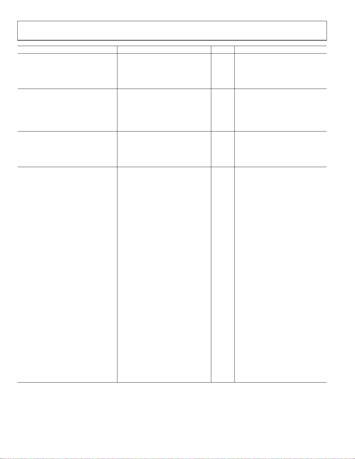
AD7262
Parameter Min Typ Max Unit Test Conditions/Comments
LOGIC INPUTS
Input High Voltage, V
Input Low Voltage, V
Input Current, IIN ±1 µA VIN = 0 V or V
Input Capacitance, C
LOGIC OUTPUTS
Output High Voltage, VOH V
Output Low Voltage, VOL 0.4 V
Floating State Leakage Current ±1 µA
Floating State Output Capacitance
Output Coding Twos complement
CONVERSION RATE
Conversion Time 19 × t
Track-and-Hold Acquisition Time 400 ns
Throughput Rate 1 MSPS AD7262
500 kSPS AD7262-5
COMPARATORS
Input Offset
Comparator A and Comparator B ±2 ±4 mV TA = 25°C to 105°C only
Comparator C and Comparator D ±2 ±4 mV
Offset Voltage Drift 0.5 V/°C All comparators
Input Common-Mode Range
0 to 1.7 V CA_CBVCC = 2.7 V
Input Capacitance
Input Impedance
IDD Normal Mode (Static)
Comparator A and Comparator B 3 µA CA_CBVCC = 3.3 V
6 8.5 µA CA_CBVCC = 5.25 V
Comparator C and Comparator D 60 µA CC_CDVCC = 3.3 V
120 170 µA CC_CDVCC = 5.25 V
Propagation Delay Time
High to Low, t
Comparator A and Comparator B 1.4 3.5 µs CA_CBVCC = 2.7 V
0.95 µs CA_CBVCC = 5 V
Comparator C and Comparator D 0.20 0.32 µs CC_CDVCC = 2.7 V
0.13 µs CC_CDVCC = 5 V
Low to High, t
Comparator A and Comparator B 2 4 µs CA_CBVCC = 2.7 V
0.93 µs CA_CBVCC = 5 V
Comparator C and Comparator D 0.18 0.28 µs CC_CDVCC = 2.7 V
0.12 µs CC_CDVCC = 5 V
Delay Matching
Comparator A and Comparator B ±250 ns
Comparator C and Comparator D ±10 ns
0.7 × V
INH
0.8 V
INL
3
IN
3
3
0 to 4 V C
3
4 pF
3
1 GΩ
6
4 pF
DRIVE
5 pF
V
DRIVE
− 0.2 V
ns
SCLK
= 5 V
A_CBVCC
25 pF load, C
V
V
= 200 mV differential
OVERDRIVE
= AVCC/2, V
CM
DRIVE
x = 0 V, VCM = AVCC/2,
OUT
OVERDRIVE
differential
PHL
PLH
= AVCC 2, V
V
CM
OVERDRIVE
differential
= 200 mV
= 200 mV
Rev. 0 | Page 4 of 32
AD7262
Parameter Min Typ Max Unit Test Conditions/Comments
POWER REQUIREMENTS Digital inputs = 0 V or V
AVCC 4.75 5.25 V
CA_CBVCC, CC_CDVCC 2.7 5.25 V
V
2.7 5.25 V
DRIVE
IDD
ADC Normal Mode (Static) 20 31.5 mA AVCC = 5.25 V
ADC Normal Mode (Dynamic) 23 33.3 mA AVCC = 5.25 V
Shutdown Mode 0.5 1 A
= 5.25 V, ADCs and comparators
AV
CC
powered down
Power Dissipation
ADC Normal Mode (Static) 105 165 mW
ADC Normal Mode (Dynamic) 120 175 mW
Shutdown Mode 2.625 5.25 µW
1
These specifications were determined without the use of the gain calibration feature.
2
See the Terminology section.
3
Samples tested during initial release to ensure compliance; they are not subject to production testing.
4
For PGA gain = 1; to use the full analog input range (VCM ± V
5
Refers to Pin V
6
This specification includes the IDD for both comparators. The IDD per comparator is the specified value divided by two.
A or Pin V
REF
B.
REF
/2) of the AD7262, the VCM voltage should be dropped to lie within a range from 1.95 V to 2.05 V.
REF
DRIVE
Rev. 0 | Page 5 of 32
AD7262
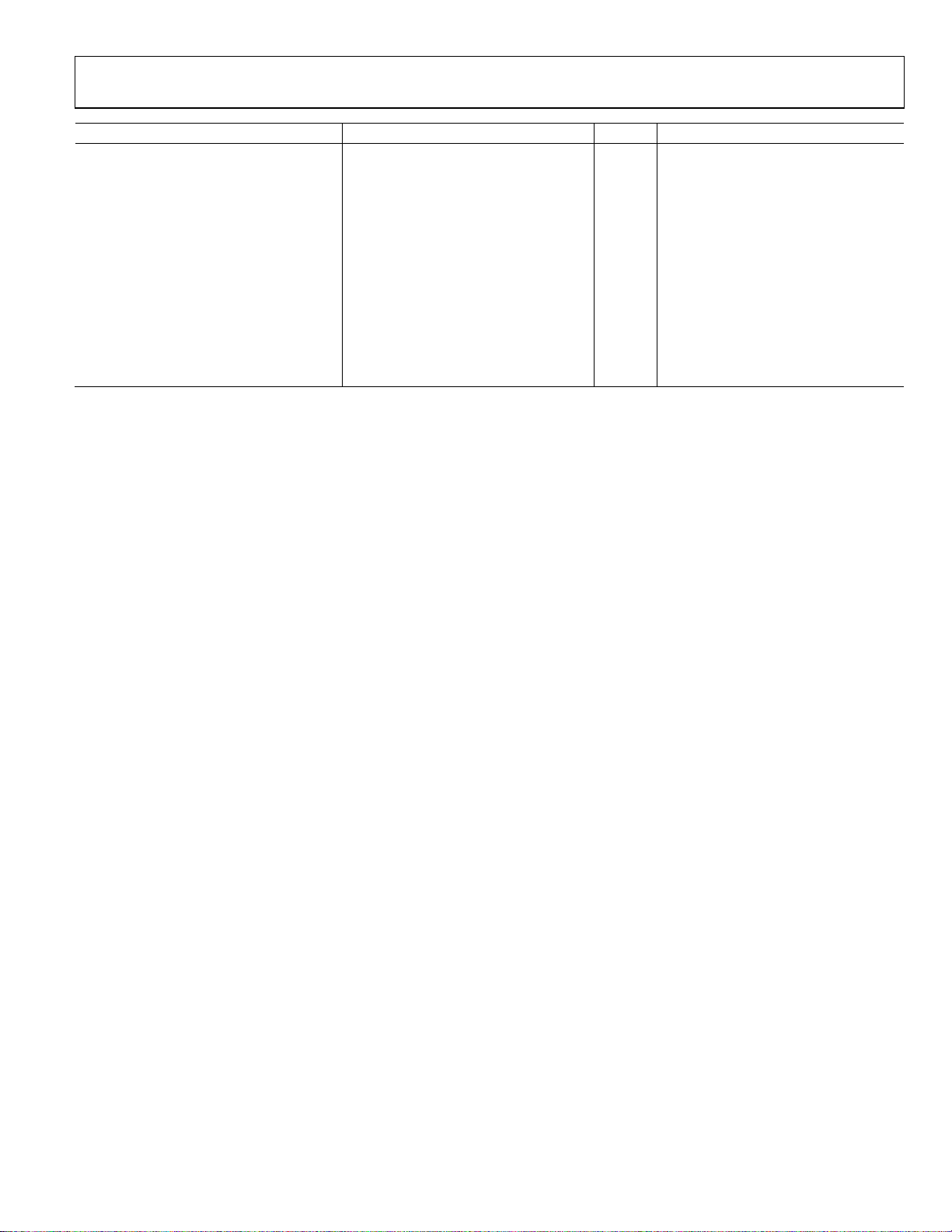
TIMING SPECIFICATIONS
AVCC = 4.75 V to 5.25 V, CA_CBVCC = CC_CDVCC = 2.7 V to 5.25 V, V
Table 2.
Limit at T
Parameter 2.7 V ≤ V
f
200 200 kHz min
SCLK
t
CONVER T
t
13 13 ns min
QUIET
t
2
3
t
3
t
29 23 ns max Data access time after SCLK falling edge
4
t
5
t
6
40 40 MHz max AD7262
32 32 MHz typ AD7262
20 20 MHz max AD7262-5
19 × t
475 475 ns max AD7262
950 950 ns max AD7262-5
10 10 ns min
15 15 ns max
15 13 ns min SCLK to data valid hold time
0.4 × t
t7 0.4 × t
≤ 3.6 V 4.75 V ≤ V
DRIVE
19 × t
SCLK
0.4 × t
SCLK
SCLK
, T
MIN
0.4 × t
MAX
≤ 5.25 V Unit Description
DRIVE
ns max t
SCLK
ns min SCLK high pulse width
SCLK
SCLK
t8 13 13 ns min
t
9
t
10
13 13 ns max
5 5 ns min SCLK falling edge to D
35 35 ns max SCLK falling edge to D
t11 2 2 s min Minimum CAL pin high time
t12 2 2 s min
t13 3 3 ns min DIN setup time prior to SCLK falling edge
t14 3 3 ns min DIN hold time after SCLK falling edge
t
240 240 s max Internal reference, with a 1 F decoupling capacitor
POWER-UP
15 15 s max With an external reference, 10 s typical
1
Sample tested during initial release to ensure compliance. All input signals are specified with tR = tF = 5 ns (10% to 90% of AVCC) and timed from a voltage level of 1.6 V.
All timing specifications given are with a 25 pF load capacitance. With a load capacitance greater than this value, a digital buffer or latch must be used. See the
Terminology section.
2
See the Serial Interface section.
3
The time required for the output to cross 0.4 V or 2.4 V.
= 2.5 V internal/external; TA = T
REF
2
2
SCLK
= 1/f
SCLK
Minimum time between end of serial read/bus relinquish
and next falling edge of CS
to SCLK setup time
CS
th
Delay from 19
SCLK falling edge until D
three-state disabled
ns min SCLK low pulse width
rising edge to falling edge pulse width
CS
rising edge to D
CS
OUT
relinquish
Minimum time between the CAL pin high and the CS
falling edge
to T
MIN
A, D
OUT
OUT
A, D
A, D
, unless otherwise noted.1
MAX
B, high impedance/bus
OUT
B, high impedance
OUT
B, high impedance
OUT
A and D
OUT
OUT
B are
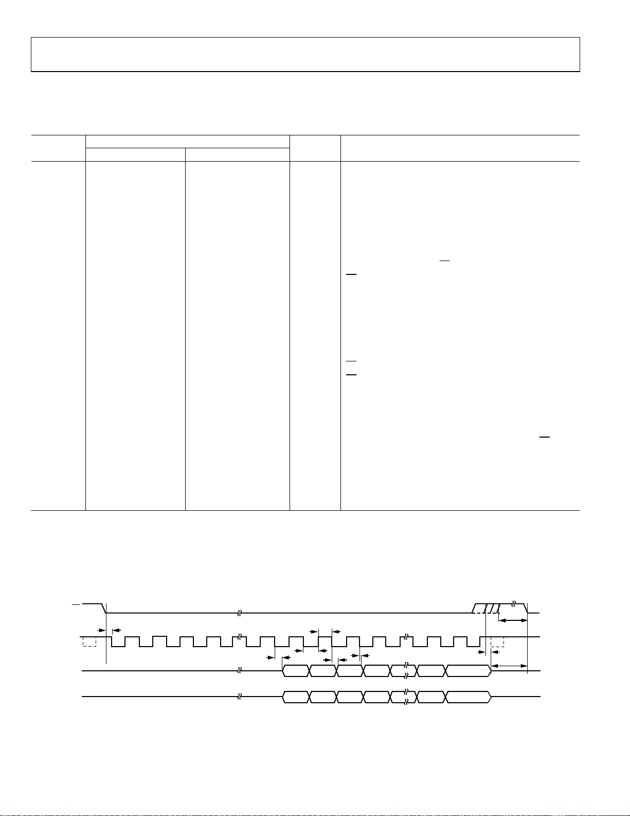
TIMING DIAGRAM
CS
SCLK
D
OUT
D
OUT
A
B
1519
t
2
234 20
THREE-STAT E
THREE-STAT E
18
t
3
Figure 2. Serial Interface Timing Diagram
Rev. 0 | Page 6 of 32
DB11
DB11
t
8
t
6
21 29 30 31
t
7
t
4
DB9
DB10
A
A
DB9
DB10
B
B
t
5
A
B
DB1
DB1
A
B
DB0
DB0
t
9
t
QUIET
A
THREESTATE
B
THREESTATE
07606-002
AD7262
ABSOLUTE MAXIMUM RATINGS
Table 3.
Parameter Rating
V
to DGND −0.3 V to AVCC
DRIVE
V
to AGND −0.3 V to AVCC
DRIVE
AVCC to AGND/DGND −0.3 V to +7 V
CA_CBVCC to CA_CB_GND −0.3 V to +7 V
CC_CDVCC to CC_CD_GND −0.3 V to +7 V
AGND to DGND −0.3 V to +0.3 V
CA_CB_GND/CC_CD_GND to DGND −0.3 V to +0.3 V
Analog Input Voltage to AGND −0.3 V to AVCC + 0.3 V
Digital Input Voltage to DGND −0.3 V to +7 V
Digital Output Voltage to GND −0.3 V to V
V
A/V
REF
C
OUT
CA±/CB±/CC±/CD± to
B Input to AGND −0.3 V to AVCC + 0.3 V
REF
A/C
B/C
C/C
OUT
OUT
D to GND −0.3 V to V
OUT
−0.3 V to
_GND/CC_CD_GND
C
A_CB
CA_CBVCC/CC_CDVCC + 0.3 V
DRIVE
DRIVE
+ 0.3 V
+ 0.3 V
Operating Temperature Range −40°C to +105°C
Storage Temperature Range −65°C to +150°C
Junction Temperature 150°C
LFCSP Package
θJA Thermal Impedance 30°C/W
θJC Thermal Impedance 3°C/W
LQFP Package
θJA Thermal Impedance 55°C/W
θJC Thermal Impedance 16°C/W
Pb-Free Temperature, Soldering
Reflow 255°C
ESD 2 kV
Stresses above those listed under Absolute Maximum Ratings
may cause permanent damage to the device. This is a stress
rating only; functional operation of the device at these or any
other conditions above those indicated in the operational
section of this specification is not implied. Exposure to absolute
maximum rating conditions for extended periods may affect
device reliability.
ESD CAUTION
Rev. 0 | Page 7 of 32

AD7262
PIN CONFIGURATIONS AND FUNCTION DESCRIPTIONS
_GND
B
A
CC
_C
A
REF
AV
AGND
C
V
42
434445
B
CC
REF
AV
_GND
AGND
V
D
_C
C
C
37G338G239G140G041
36
CAL
35
CS
34
SCLK
33
AV
CC
32
D
A
OUT
31
D
B
OUT
30
C
A
OUT
C
B
29
OUT
DGND
28
27
V
DRIVE
26
C
C
OUT
25
C
D
OUT
IN
PD2
PD1
PD0/D
REFSEL
7606-003
CA_CBV
CC_CDV
NOTES
1. THE EXPOSED METAL PADDLE ON THE BOTTOM OF THE L FCSP PACKAGE MUST
BE SOLDERED T O PCB GROUND F OR PROPER HEAT DISSIPATION AND ALSO FOR
NOISE AND MECHANICAL STRENGT H BENEFITS.
AV
VA–
V
AGND
AGND
AV
AGND
V
VB–
AV
1
CC
2
CC
3
+
4
A
5
6
7
CC
8
+
9
B
10
11
CC
12
CC
CA_CBV
AGND
AGND
AGND
CC_CDV
AV
AV
AV
–
+
–
+
B
B
A
A
C
C
C
C
46
47
48
1
VA–
V
V
VB–
CC
CC
+
A
CC
+
B
CC
CC
PIN 1
2
INDICATO R
3
4
5
6
7
8
9
10
11
12
13 15 16 17 18 19 20 21 22 23 24
14
+
C
C
–
C
C
AD7262
TOP VIEW
(Not to Scale)
–
+
D
D
C
C
Figure 3. 48-Lead LQFP Pin Configuration Figure 4. 48-Lead LFCSP Pin Configuration
Table 4. Pin Function Descriptions
Pin No. Mnemonic Description
2, 7, 11, 20, 33, 41 AVCC
Analog Supply Voltage, 4.75 V to 5.25 V. This is the supply voltage for the analog circuitry on the
AD7262/AD7262-5. All AV
pins can be tied together. This supply should be decoupled to AGND
CC
with a 100 nF ceramic capacitor per supply and a 10 F tantalum capacitor.
1 CA_CBVCC
Comparator Supply Voltage, 2.7 V to 5.25 V. This is the supply voltage for Comparator A and
Comparator B. This supply should be decoupled to C
tied together.
12 C
C_CDVCC
Comparator Supply Voltage, 2.7 V to 5.25 V. This is the supply voltage for Comparator C and
Comparator D. This supply should be decoupled to C
tied together.
4, 3 VA+, VA− Analog Inputs of ADC A. True differential input pair.
9, 10 V
43, 18 V
+, VB− Analog Inputs of ADC B. True differential input pair.
B
A, V
REF
REF
B
Reference Input/Output. Decoupling capacitors are connected to these pins to decouple the
internal reference buffer for each respective ADC. Typically, 1 F capacitors are required to decouple
the reference. Provided the output is buffered, the on-chip reference can be taken from these pins
and applied externally to the rest of a system.
34 SCLK
Serial Clock. Logic input. A serial clock input provides the SCLK for accessing the data from the
AD7262/AD7262-5. This clock is also used as the clock source for the conversion process. A
minimum of 31 clocks is required to perform the conversion and access the 12-bit result.
36 CAL
21 PD2
Logic Input. Initiates an internal offset calibration.
Logic Input. Places the AD7262/AD7262-5 in selected shutdown mode in conjunction with the PD1
and PD0 pins (see Table 7).
22 PD1
Logic Input. Places the AD7262/AD7262-5 in selected shutdown mode in conjunction with the PD2
and PD0 pins (see Table 7).
_GND
B
A
–
+
–
+
A
C
4847464544434241403938
13141516171819
+
C
C
A_CB
C_CD
_C
B
B
A
A
REF
C
C
PIN 1
INDICAT OR
–
+
C
D
C
C
C
C
V
AD7262
TOP VIEW
(Not to Scale)
–
B
D
C
REF
_GND
AGND
V
D
_C
C
C
AVCCAGND
2021222324
CC
AV
G0
PD2
G1
PD1
G3
G2
37
CAL
36
CS
35
SCLK
34
AV
33
D
32
D
31
C
30
C
29
DGND
28
V
27
C
26
C
25
IN
PD0/D
REFSEL
_GND. AVCC, CC_CDVCC, and CA_CBVCC can be
_GND. AVCC, CC_CDVCC, and CA_CBVCC can be
CC
OUT
OUT
OUT
OUT
DRIVE
OUT
OUT
A
B
A
B
C
D
07606-004
Rev. 0 | Page 8 of 32
AD7262
Pin No. Mnemonic Description
23 PD0/DIN
35
48, 47, 46, 45
13, 14, 15, 16
CS
+, CA−,
C
A
+, CB−
C
B
+, CC−,
C
C
+, CD−
C
D
5, 6, 8, 19, 42 AGND
28 DGND
30, 29, 26, 25
32, 31 D
A, C
C
OUT
OUT
C, C
C
OUT
OUT
A, D
OUT
OUT
40, 39, 38, 37 G0, G1, G2, G3
27 V
44, 17
C
C
DRIVE
A_CB
C_CD
_GND,
_GND
24 REFSEL
Logic Input/Data Input. Places the AD7262/AD7262-5 in selected shutdown mode in conjunction
with the PD2 and PD1 pins (see Table 7). If all gain selection pins, G0 to G3, are tied low, this pin acts
as the data input pin, and all programming is via the control register (see Table 8). Data to be written
to the AD7262/AD7262-5 control register is provided on this input and is clocked into the register
on the falling edge of SCLK.
Chip Select. Active low logic input. This input initiates conversions on the AD7262/AD7262-5.
Comparator Inputs. These pins are the inverting and noninverting analog inputs for Comparator A
and Comparator B. These two comparators have very low power consumption.
Comparator Inputs. These pins are the inverting and noninverting analog inputs for Comparator C
and Comparator D. This pair of comparators offers very fast propagation delays.
Analog Ground. Ground reference point for all analog circuitry on the AD7262/AD7262-5. All
analog input signals and any external reference signal should be referred to this AGND voltage.
All AGND pins should connect to the AGND plane of a system. The AGND, DGND, C
C
_GND voltages ideally should be at the same potential and must not be more than 0.3 V apart,
C_CD
even on a transient basis. C
_GND and CC_CD_GND can be tied to AGND.
A_CB
A_CB
Digital Ground. This is the ground reference point for all digital circuitry on the AD7262/AD7262-5.
The DGND pin should be connected to the DGND plane of a system. The DGND and AGND voltages
should ideally be at the same potential and must not be more than 0.3 V apart, even on a transient
basis.
Comparator Outputs. These pins provide a CMOS (push-pull) output from each respective
B,
D
comparator. These are digital output pins with logic levels determined by the V
B
Serial Data Outputs. The data output from the AD7262/AD7262-5 is supplied to each pin as a serial
DRIVE
supply.
data stream in twos complement format. The bits are clocked out on the falling edge of the SCLK
input. A total of 31 SCLKs is required to perform the conversion and access the 12-bit data. During
the conversion process, the data output pins are in three-state and, when the conversion is
completed, the 19
th
SCLK edge clocks out the MSB. The data simultaneously appears on both pins
from the simultaneous conversions of both ADCs. The data is provided MSB first. If CS
an additional 12 SCLK cycles on either D
the other ADC follows on the D
pin. This allows data from a simultaneous conversion on both
OUT
ADCs to be gathered in serial format on either D
OUT
A or D
B following the initial 31 SCLKs, the data from
OUT
OUT
A or D
B using only one serial port.
OUT
Logic Inputs. These pins are used to program the gain setting of the front-end amplifiers. If all four
pins are tied low, the PD0 pin acts as a data input pin, DIN, and all programming is made via the
control register (see Table 6 ).
Logic Power Supply Input, 2.7 V to 5.25 V. The voltage supplied at this pin determines at what
voltage the interface operates, including the comparator outputs. This pin should be decoupled to
DGND.
Comparator Ground. This is the ground reference point for all comparator circuitry on the AD7262/
AD7262-5. Both the CA_CB_GND pin and the CC_CD_GND pin should connect to the GND plane of a
system and can be tied to AGND. The DGND, AGND, C
_GND, and CC_CD_GND voltages should
A_CB
ideally be at the same potential and must not be more than 0.3 V apart, even on a transient basis.
Internal/External Reference Selection. Logic input. If this pin is tied to a logic high voltage, the on-
chip 2.5 V reference is used as the reference source for both ADC A and ADC B. If the REFSEL pin is
tied to GND, an external reference can be supplied to the AD7262/AD7262-5 through the V
and/or V
REF
B pin.
_GND, and
is held low for
A
REF
Rev. 0 | Page 9 of 32
AD7262
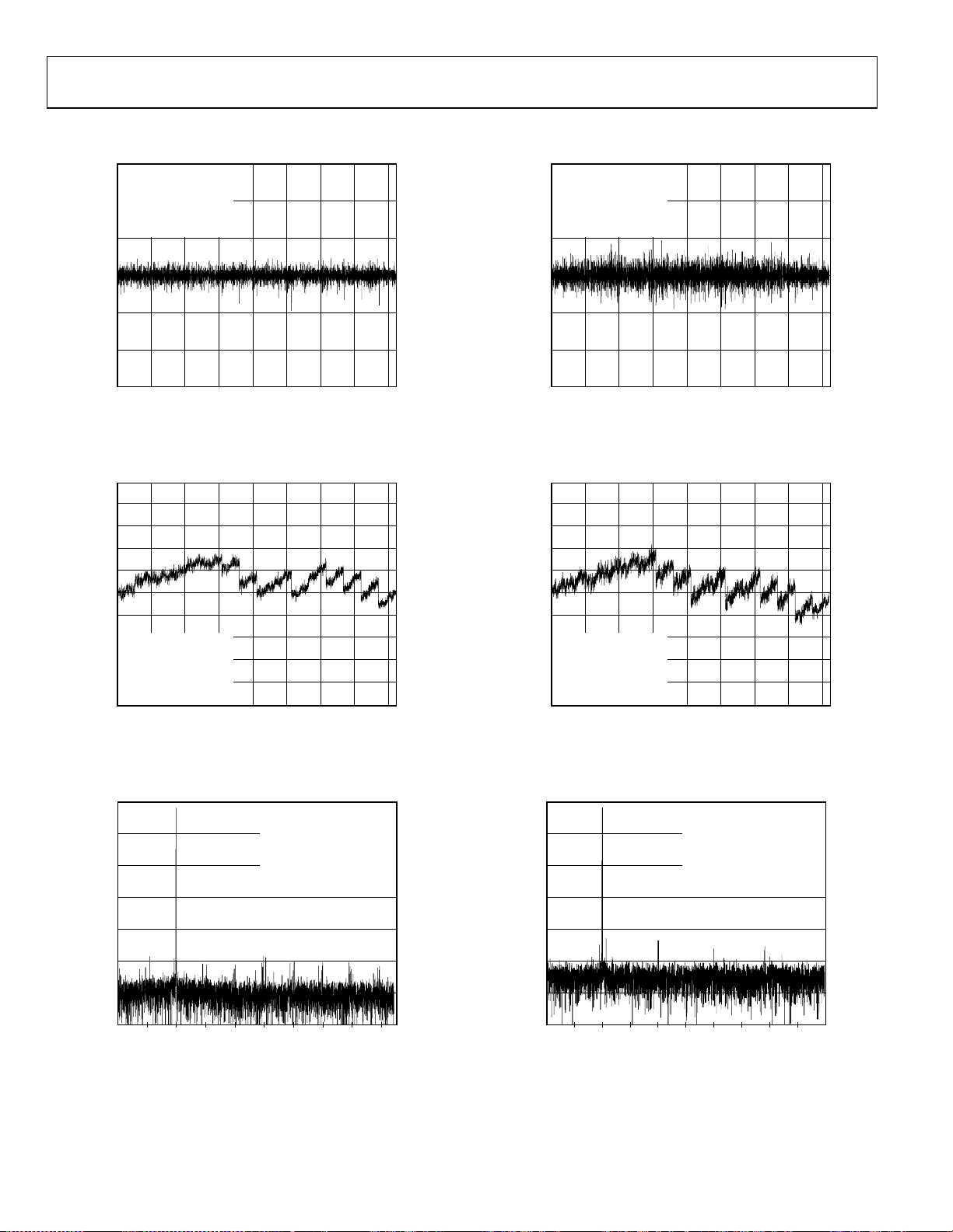
TYPICAL PERFORMANCE CHARACTERISTICS
0.6
AVCC = 5V
V
= 5V
DRIVE
f
= 1MSPS
S
0.4
T
= 25°C
A
INTERNAL REFERENCE
PGA GAIN = 2
0.2
0.6
AVCC = 5V
V
= 5V
DRIVE
f
= 1MSPS
S
0.4
T
= 25°C
A
INTERNAL REFERENCE
PGA GAIN = 32
0.2
0
–0.2
DNL ERRO R (LSB)
–0.4
–0.6
0400035003000250020001 5001000500
1.0
0.8
0.6
0.4
0.2
0
–0.2
INL ERROR (LS B)
–0.4
AVCC = 5V
V
DRIVE
–0.6
f
= 1MSPS
S
T
= 25°C
A
–0.8
INTERNAL REFERENCE
PGA GAIN = 2
–1.0
0400035003000250020001 5001000500
CODE
Figure 5. Typical DNL at Gain of 2
= 5V
CODE
Figure 6. Typical INL at Gain of 2
0
–0.2
DNL ERRO R (LSB)
–0.4
–0.6
0435003000250020001 5001000500
07606-005
CODE
000
07606-008
Figure 8. Typical DNL at Gain of 32
1.0
0.8
0.6
0.4
0.2
0
–0.2
INL ERROR (LS B)
–0.4
AVCC = 5V
V
= 5V
DRIVE
–0.6
f
= 1MSPS
S
T
= 25°C
A
–0.8
INTERNAL REFERENCE
PGA GAIN = 32
–1.0
0435003000250020001 5001000500
07606-006
CODE
000
07606-009
Figure 9. Typical INL at Gain of 32
0
–20
–40
–60
(dB)
–80
–100
–120
–140
0 400k 450k350k300k250k200k150k100k50k
FREQUENCY (Hz)
AVCC = 5V
V
= 2.7V
DRIVE
f
= 1MSPS
S
T
= 25°C
A
f
= 100kHz
IN
INTERNAL REFERENCE
SNR = 73dB, T HD = –82.5dB
PGA GAIN = 2
07606-007
Figure 7. 3 dB Typical FFT at Gain of 2
0
–20
–40
–60
(dB)
–80
–100
–120
–140
0 400k 450k 500k350k300k250k200k150k100k50k
AVCC = 5V
V
= 5V
DRIVE
f
= 1MSPS
S
T
= 25°C
A
f
= 100kHz
IN
INTERNAL REFERENCE
SNR = 68.38dB, THD = –82dB
PGA GAIN = 32
FREQUENCY (Hz)
07606-010
Figure 10. Typical FFT at Gain of 32
Rev. 0 | Page 10 of 32

AD7262
–
9000
8000
7000
6000
5000
4000
3000
NUMBER OF HITS
2000
1000
0
0
8839
828
333
2043 2044 2045
CODE
0
Figure 11. Histogram of Codes for 10k Samples at Gain of 2
07606-011
2.4968
2.4967
2.4966
2.4965
(V)
REF
2.4964
V
2.4963
AVCC = 5V
2.4962
V
= 3V
DRIVE
f
= 1MSPS
S
INTERNAL REFERENCE
2.4961
0 20 40 60 80 100 120 140 160 180 200
CURRENT LOAD ( µA)
Figure 14. V
vs. Reference Output Current Load
REF
07606-014
8000
7000
6000
5000
4000
3000
NUMBER OF HITS
2000
1000
0
1297
0
20452044 2046 2047 2048 2049
6967
CODE
1732
40
07606-012
Figure 12. Histogram of Codes for 10k Samples at Gain of 32
50
AV
= 5V
CC
V
= 5V
DRIVE
–55
f
= 1MSPS
S
INTERNAL REFERENCE
–60
–65
–70
THD (dB)
–75
–70
–85
–90
10 910810710610510410310210110
ANALOG INPUT FREQUENCY (kHz)
GAIN = 32
GAIN = 2
07606-013
Figure 13. THD vs. Analog Input Frequency up to 1 MHz at Gain of 2 and 32
1900
1800
1700
1600
1500
1400
1300
1200
1100
1000
3dB BANDWIDTH (kHz)
900
AVCC = 5V
800
700
600
= 5V
V
DRIVE
f
= 1MSPS
S
INTERNAL REFERENCE
2 3 4 6 8 12 16 24 32 48 64 96 128
1
GAIN
Figure 15. 3 dB Bandwidth vs. Gain
80
75
70
65
60
55
SNR (dB)
50
45
AVCC = 5V
40
35
30
= 5V
V
DRIVE
f
= 1MSPS
S
INTERNAL REFERENCE
= 100kHz
F
IN
1 2 3 4 6 8 12 16 24 32 48 64 96 128
PGA GAIN
Figure 16. SNR vs. PGA Gain for an Analog Input Tone of 100 kHz
07606-015
07606-016
Rev. 0 | Page 11 of 32

AD7262
–
–
–
–
90
–88
–86
–84
–82
–80
CMR (dB)
–78
–76
–74
–72
–70
1 2 3 4 6 8 12 16 24 32 48 64 96 128
AVCC = 5V
V
DRIVE
f
= 1MSPS
S
INTERNAL REFERENCE
f
RIPPLE
GAIN
Figure 17. Common-Mode Rejection vs. Gain
= 5V
= 50kHz
07606-017
10
9
8
7
6
5
4
3
PROPAG ATIO N DELAY (µs)
2
H TO L, C
A_CBVCC
H TO L, C
A_CBVCC
H TO L, C
A_CBVCC
H TO L, C
A_CBVCC
L TO H, C
A_CBVCC
L TO H, C
A_CBVCC
L TO H, CA_CBVCC = 4.5V
L TO H, C
A_CBVCC
AVCC = 5V
V
DRIVE
T
A
= 3.6V
= 4.5V
= 2.7V
= 5V
= 2.7V
= 3.6V
= 5V
= 3.3V
= 25°C
1
0
0 102030405060708090100
OVERDRIVE VOLTAGE (mV)
Figure 20. Propagation Delay for Comparator A and Comparator B vs.
Overdrive Voltage for Various Supply Voltages
07606-020
80
–79
–78
–77
–76
–75
CMR (dB)
–74
–73
–72
–71
–70
0 20 40 60 80 100 120 140 160 180 200
RIPPLE FREQUENCY (kHz)
AVCC = 5V
= 5V
V
DRIVE
f
= 1MSPS
S
= 700mV p-p
V
RIPPLE
GAIN = 2
INTERNAL REFERENCE
07606-018
Figure 18. Common-Mode Rejection vs. Common-Mode Ripple Frequency
10
AVCC = 5V
V
= 5V
DRIVE
–20
f
= 1MSPS
S
INTERNAL REFERENCE
–30
f
= 100kHz
IN
–40
–50
–60
THD (dB)
–70
–80
GAIN 8
GAIN 4
–90
GAIN 12
–100
1.3 1.5 1.7 1.9 2.1 2.3 2.5 2.7 2. 9 3.1 3.3 3 .5 3.7
GAIN 24
V
CM
GAIN ≥ 32
RANGE (V)
GAIN 1
GAIN 2
GAIN 3
GAIN 16
GAIN 6
07606-019
Figure 19. THD vs. Common-Mode Range for Various PGA Gain Settings
2.0
1.8
1.6
1.4
1.2
1.0
0.8
0.6
PROPAG ATIO N DELAY (µs)
0.4
L TO H, C
L TO H, C
L TO H, C
L TO H, C
H TO L, C
H TO L, C
H TO L, C
H TO L, CC_CDVCC = 4.5V
C_CDVCC
C_CDVCC
C_CDVCC
C_CDVCC
C_CDVCC
C_CDVCC
C_CDVCC
AVCC = 5V
V
= 3.3V
DRIVE
T
= 25°C
A
= 2.7V
= 3.6V
= 4.5V
= 5V
= 2.7V
= 3.6V
= 5V
0.2
0
0 102030405060708090100
OVERDRIVE VOLTAGE (mV)
Figure 21. Propagation Delay for Comparator C and Comparator D vs.
Overdrive Voltage for Various Supply Voltages
70
V
= 5V
DRIVE
GAIN = 2
–75
T
= 25°C
A
INTERNAL REFERENCE
–80
100mV p-p SINE WAVE ON AV
AVCC DECOUPLED WI TH
–85
10µF AND 100nF CAPACITORS
CC
–90
–95
PSRR (dB)
–100
–105
–110
–115
–120
0 200 400 600 800 1000
SUPPLY RIPPLE FREQUENCY (kHz)
Figure 22. Power Supply Rejection Ratio vs. Supply Ripple Frequency?
07606-021
07606-022
Rev. 0 | Page 12 of 32

AD7262
300
C
A/C
B SINK CURRENT
OUT
C/C
D SINK CURRENT
OUT
SINK CURRENT
SOURCE CURRENT
A/C
B SOURCE CURRENT
OUT
C/C
D SOURCE CURRENT
OUT
0.2
0.4
0.6
0.3
0.5
0.7
OUT
0.8
1.0
1.2
0.9
1.1
1.3
CURRENT (mA)
and C
Source and Sink Current
OUT
1.4
1.5
1.6
1.7
1.8
1.9
2.0
2.1
2.2
2.3
2.4
2.5
07606-023
(mV)
OUT
– V
DD
–100
(V) OR V
OUT
V
–200
–300
200
100
0
OUT
C
OUT
D
OUT
D
OUT
C
OUT
C
OUT
0
0.1
Figure 23. D
Rev. 0 | Page 13 of 32

AD7262
TERMINOLOGY
Differential Nonlinearity (DNL)
Differential nonlinearity is the difference between the measured
and the ideal 1 LSB change between any two adjacent codes in
the ADC.
Integral Nonlinearity (INL)
Integral nonlinearity is the maximum deviation from a straight
line passing through the endpoints of the ADC transfer function.
The endpoints of the transfer function are zero scale, a single
(1) LSB point below the first code transition and full scale, a single
(1) LSB point above the last code transition.
Zero Code Error
This is the deviation of the midscale transition (all 1s to all 0s)
from the ideal V
voltage, that is, V
IN
– ½ LSB.
CM
Positive Full-Scale Error
This is the deviation of the last code transition (011 … 110) to
(011 … 111) from the ideal, that is,
V
REF
×+Gain
⎞
LSB12−
⎟
⎠
⎛
V
⎜
CM
⎝
after the zero code error has been adjusted out.
Negative Full-Scale Error
This is the deviation of the first code transition (10 … 000) to
(10 … 001) from the ideal, that is,
V
REF
×−Gain
⎞
LSB12+
⎟
⎠
⎛
V
⎜
CM
⎝
after the zero code error has been adjusted out.
Zero Code Error Match
This is the difference in zero code error across both ADCs.
Positive Full-Scale Error Match
This is the difference in positive full-scale error across both ADCs.
Negative Full-Scale Error Match
This is the difference in negative full-scale error across both ADCs.
Track-and-Hold Acquisition Time
The track-and-hold amplifier returns to track mode at the end
of a conversion. Track-and-hold acquisition time is the time
required for the output of the track-and-hold amplifier to reach
its final value, within ±1/2 LSB, after the end of a conversion.
Signal-to-(Noise + Distortion) Ratio
This ratio is the measured ratio of signal-to-(noise + distortion)
at the output of the analog-to-digital converter. The signal is the
rms amplitude of the fundamental. Noise is the sum of all nonfundamental signals up to half the sampling frequency (f
/2),
S
excluding dc. The ratio is dependent on the number of quantization levels in the digitization process; the more levels, the
smaller the quantization noise. The theoretical signal-to-(noise +
distortion) ratio for an ideal N-bit converter with a sine wave
input is given by
Signal-to-(Noise + Distortion) = (6.02N + 1.76) dB
Thus for a 12-bit converter, this is 86 dB.
Rev. 0 | Page 14 of 32
Total Harmonic Distortion (THD)
Total harmonic distortion is the ratio of the rms sum of harmonics
to the fundamental. For the AD7262/AD7262-5, it is defined as
2
2
2
2
where
V
, V
4
2
THD
V
, and V
5
=
is the rms amplitude of the fundamental, and V2, V3,
1
are the rms amplitudes of the second through the
6
2
log20(dB)
4
3
V
1
++++
VVVVV
6
5
sixth harmonics.
Peak Harmonic or Spurious Noise
Peak harmonic, or spurious noise, is defined as the ratio of the
rms value of the next largest component in the ADC output
spectrum (up to f
/2, excluding dc) to the rms value of the fun-
S
damental. Normally, the value of this specification is determined
by the largest harmonic in the spectrum, but for ADCs where
the harmonics are buried in the noise floor, it is a noise peak.
ADC-to-ADC Isolation
ADC-to-ADC isolation is a measure of the level of crosstalk
between the ADC A and ADC B. It is measured by applying a
full-scale, 100 kHz sine wave signal to all unselected input channels
and determining how much that signal is attenuated in the
selected channel with a 40 kHz signal. The figure given is the
worst case.
PSRR (Power Supply Rejection)
Variations in power supply affect the full-scale transition but
not the linearity of the converter. Power supply rejection is the
maximum change in the full-scale transition point due to a
change in power supply voltage from the nominal value (see
Figure 22).
Propagation Delay Time, Low to High (t
PLH
)
Propagation delay time from low to high is defined as the time
taken from the 50% point on a low to high input signal until the
digital output signal reaches 50% of its final low value.
Propagation Delay Time, High to Low (t
PHL
)
Propagation delay time from high to low is defined as the time
taken from the 50% point on a high to low input signal until the
digital output signal reaches 50% of its final high value.
Comparator Offset
Comparator offset is the measure of the density of digital 1s
and 0s in the comparator output when the negative analog
terminal of the comparator input is held at a static potential
and the analog input to the positive terminal of the comparators
is varied proportionally about the static negative terminal voltage.

AD7262
THEORY OF OPERATION
CIRCUIT INFORMATION
The AD7262/AD7262-5 are fast, dual, simultaneous sampling,
differential, 12-bit, serial ADCs. The AD7262/ AD7262-5
contain two on-chip differential programmable gain amplifiers,
two track-and-hold amplifiers, and two successive approximation analog-to-digital converters with a serial interface with two
separate data output pins. The AD7262/ AD7262-5 also include
four on-chip comparators. They are housed in 48-lead LFCSP
and LQFP packages, offering the user considerable space-saving
advantages over alternative solutions. The AD7262/AD7262-5
require a low voltage 5 V ± 5% AV
supply the digital power, a 5.25 V to 2.7 V C
supply for the comparators, and a 2.7 V to 5.25 V V
to power the ADC core and
CC
A_CBVCC
, CC_CDVCC
supply
DRIVE
for interface power.
The on-board PGA allows the user to select from 14 programmable gain stages: ×1, ×2, ×3, ×4, ×6, ×8, ×12, ×16, ×24, ×32,
×48, ×64, ×96, and ×128. The PGA accepts fully differential
analog signals. The gain can be selected either by setting the
logic state of the G0 to G3 pins or by programming the control
register.
The serial clock input accesses data from the part while also
providing the clock source for each successive approximation
ADC. The AD7262/AD7262-5 have an on-chip 2.5 V reference
that can be disabled when an external reference is preferred. If
the internal reference is used elsewhere in a system, the output
from V
A and V
REF
B must first be buffered. If the internal
REF
reference is the preferred option, the user must tie the
REFSEL pin to a logic high voltage. Alternatively, if REFSEL
is tied to GND, an external reference can be supplied to both
ADCs through the V
A and V
REF
B pins (see the Reference
REF
section).
The AD7262/AD7262-5 also feature a range of power-down
options to allow the user great flexibility with the independent
circuit components while allowing for power savings between
conversions. The power-down feature is implemented via the
control register or the PD0 to PD2 pins, as described in the
Control Register section.
COMPARATORS
The AD7262/AD7262-5 have four on-chip comparators. Comparator A and Comparator B have ultralow power consumption,
with static power consumption typically less than 10 W with a
3.3 V supply. Comparator C and Comparator D feature ver y fast
propagation delays of 130 ns for a 200 mV differential overdrive.
These comparators have push-pull output stages that operate
from the V
minimum amount of power consumption.
supply. This feature allows operation with a
DRIVE
Each pair of comparators operates from its own independent
supply, C
A_CBVCC
for supply voltages from 2.7 V to 5.25 V. If desired, C
and C
C_CDVCC
rators on the AD7262/AD7262-5 are functional with C
C
C_CDVCC
and CC_CDVCC. The comparators are specified
A_CBVCC
can be tied to the AVCC supply. The four compa-
A_CBVCC
greater than or equal to 1.8 V. However, no specifications are guaranteed for comparator supplies less than 2.7 V.
The wide range of supply voltages ensures that the comparators
can be used in a variety of battery backup modes.
The four on-chip comparators on the AD7262/AD7262-5 are
ideally suited for monitoring signals from pole sensors in motor
control systems. The comparators can be used to monitor
signals from Hall effect sensors or the inner tracks from an
optical encoder. One of the comparators can be used to count
the index marker or z marker, which is used on startup to place
the motor in a known position.
OPERATION
The AD7262/AD7262-5 have two successive approximation
ADCs, each based around two capacitive DACs and two
programmable gate amplifiers.
The ADC itself comprises control logic, a SAR, and two capacitive
DACs. The control logic and the charge redistribution DACs are
used to add and subtract fixed amounts of charge from the sampling capacitor amplifiers to bring the comparator back into a
balanced condition. When the comparator is rebalanced, the
conversion is complete. The control logic generates the ADC
output code.
Each ADC is preceded by its own programmable gain stage. The
PGA features high analog input impedance, true differential analog
inputs that allow the output from any source or sensor to be
connected directly to the PGA inputs without any requirement for
additional external buffering. The variable gain settings ensure
that the device can be used for amplifying signals from a variety
of sources. The AD7262/AD7262-5 offer the flexibility to choose
the most appropriate gain setting to use the wide dynamic range
of the device.
ANALOG INPUTS
Each ADC in the AD7262/AD7262-5 has two high impedance
differential analog inputs. Figure 24 shows the equivalent circuit
of the analog input structure of the AD7262/AD7262-5. It consists
of a fully differential input amplifier that buffers the analog input
signal and provides the gain selected by using the gain pins or
the control register.
/
Rev. 0 | Page 15 of 32

AD7262
V
V
The two diodes provide ESD protection. Care must be taken to
ensure that the analog input signals never exceed the supply rails
by more than 300 mV. Exceeding 300 mV causes these diodes to
become forward-biased and to start conducting current into the
substrate. These diodes can conduct up to 10 mA without
causing irreversible damage to the part. The C1 capacitors in
Figure 24 are typically 5 pF and can primarily be attributed to
pin capacitance.
DD
+
IN
C1
V
DD
–
V
IN
C1
Figure 24. Analog Input Structure
AMP
AMP
+
V
OUT
–
V
OUT
07606-024
The AD7262/AD7262-5 can accept differential analog inputs from
V
REF
×−Gain
⎞
V
to
⎟
CM
⎠
⎛
V
⎜
CM
2
⎝
⎛
⎜
2
⎝
V
REF
×+Gain
⎞
⎟
⎠
Tabl e 5 details the analog input range for the AD7262/AD7262-5
for the various PGA gain settings. Here, V
2.5 V (AV
/2, with AVCC = 5 V).
CC
= 2.5 V and VCM =
REF
Table 5. Analog Input Range for Various PGA Gain Settings
PGA Gain Setting Analog Input Range for VIN+ and VIN−
1 0.75 V to 3.25 V1
2 1.875 V to 3.125 V
3 2.083 V to 2.916 V
4 2.187 V to 2.813 V
6 2.292 V to 2.708 V
8 2.344 V to 2.656 V
12 2.396 V to 2.604 V
16 2.422 V to 2.578 V
24 2.448 V to 2.552 V
32 2.461 V to 2.539 V
48 2.474 V to 2.526 V
64 2.480 V to 2.520 V
96 2.487 V to 2.513 V
128 2.490 V to 2.510 V
1
For VCM = 2 V. If VCM = AVCC /2, the analog input range for VIN+ and VIN− is 1.6 V
to 3.4 V.
When a full-scale step input is applied to either differential input
on the AD7262/AD7262-5 while the other analog input is held
at a constant voltage, 3 s of settling time is typically required
prior to capturing a stable digital output code.
Transfer Function
The AD7262/AD7262-5 output is twos complement, and the
ideal transfer characteristic is shown in Figure 25. The designed
code transitions occur at successive integer LSB values (that is,
1 LSB, 2 LSB, and so on). The LSB size is dependent on the analog
input range selected. The LSB size for the AD7262/AD7262-5 is
shown in the following equation:
⎛
⎛
⎜
V
⎜
⎜
⎝
×
2
⎜
⎜
⎜
⎝
CM
V
⎛
REF
+
⎜
×
Gain
⎝
⎛
⎞
⎞
V
⎜
⎟
⎟
⎠
⎝
⎠
4096
CM
V
⎛
−−
⎜
×
22
⎝
REF
Gain
⎞
⎞
⎞
⎟
⎟
⎟
⎠
⎟
⎠
⎟
⎟
⎟
⎠
011...111
011...110
000...001
000...000
111.. .111
ADC CODE
100...010
100...001
100...000
0V
NOTES
1. FULL-SCALE RANGE (FSR) = V
Figure 25. Twos Complement Transfer Function
V
DRIVE
The AD7262/AD7262-5 have a V
voltage at which the serial interface operates. V
(V
ANALOG INPUT
IN
CM
+ – VIN–.
feature to control the
DRIVE
+ (FSR/2)) – 1LSB(VCM – (FSR/2)) + 1LSB
07606-025
allows the
DRIVE
ADC and the comparators to easily interface to both 3 V and
5 V processors. For example, when the AD7262/AD7262-5 are
operated with AV
= 5 V, the V
CC
pin can be powered from
DRIVE
a 3 V supply, allowing a large analog input range with low voltage
digital processors.
Rev. 0 | Page 16 of 32

AD7262
REFERENCE
The AD7262/AD7262-5 can operate with either the internal
2.5 V on-chip reference or an externally applied reference. The
logic state of the REFSEL pin determines whether the internal
reference is used. The internal reference is selected for both ADCs
when the REFSEL pin is tied to logic high. If the REFSEL pin is
tied to AGND, an external reference can be supplied through
the V
A and/or V
REF
must be tied to either a low or high logic state for the part to
operate. Suitable reference sources for the AD7262/AD7262-5
include AD780, AD1582, ADR431, REF193, and ADR391.
The internal reference circuitry consists of a 2.5 V band gap
reference and a reference buffer. When the AD7262/AD7262-5
are operated in internal reference mode, the 2.5 V internal
reference is available at the V
be decoupled to AGND using a 1 F capacitor. It is recommended
that the internal reference be buffered before applying it elsewhere
in the system. The internal reference is capable of sourcing up
to 90 A of current when the converter is static. If the internal
reference operation is required for the ADC conversion, the
REFSEL pin must be tied to logic high on power-up. The reference buffer requires 240 µs to power up and charge the 1 F
decoupling capacitor during the power-up time.
B pins. On power-up, the REFSEL pin
REF
A and V
REF
B pins, which should
REF
TYPICAL CONNECTION DIAGRAMS
Figure 26 and Figure 27 are typical connection diagrams for the
AD7262/AD7262-5. In these configurations, the AGND pin is
connected to the analog ground plane of the system, and the
DGND pin is connected to the digital ground plane of the system.
The analog inputs on the AD7262/AD7262-5 are true differential and have an input impedance in excess of 1 G; thus, no
driving op amps are required. The AD7262/AD7262-5 can operate
with either an internal or an external reference. In Figure 26, the
AD7262/AD7262-5 are configured to operate in control register
mode; thus, G0 to G3, PD1, and PD2 can be connected to ground
(low logic state). Figure 27 has the gain pins configured for a gain
of 2 setup; thus, the device is in pin-driven mode. Both circuit
configurations illustrate the use of the internal 2.5 V reference
The C
A_CBVCC
a 3 V or a 5 V supply voltage. The AV
to a 5 V supply. All supplies should be decoupled with a 100 nF
capacitor at the device pin, and some supply sources may require a
10 F capacitor where the source is supplied to the circuit board.
The V
DRIVE
processor. The voltage applied to the V
voltage of the serial interface. V
and the CC_CDVCC pins can be connected to either
pin must be connected
CC
pin is connected to the supply voltage of the micro-
input controls the
DRIVE
can be set to 3 V or 5 V.
DRIVE
Rev. 0 | Page 17 of 32

AD7262
V
V
– AND VA+
A
CONNECT
DIRECTLY
TO SENSOR
OUTPUTS
THIS REFERENCE SIGNAL
MUST BE BUFFERED
BEFORE IT CAN BE
USED ELSEWHERE IN
VB– AND VB+
CONNECT
DIRECTLY
TO SENSOR
OUTPUTS
3.125V
2.500V
1.875V
3.125V
2.500V
1.875V
THE CIRCUIT
3.125V
2.500V
1.875V
3.125V
2.500V
1.875V
GAIN 2
GAIN 2
GAIN 2
GAIN 2
ANALOG
SUPPLY
43
1µF
18
1µF
10
+5
1
100nF
10µF
100nF
100nF
100nF
100nF
17 44 5 6 8 19 42 28 2 7 11 20 41 12 1 33
GND
GND
AGND
AGND
AGND
D–
B–
C
C
C–
A–
C
3
4
C
V
–
A
+
V
A
V
A
REF
AGND
AGND
DGND
CCAVCCAVCCAVCCAVCC
AV
AD7262
V
B
REF
9
V
+
B
VB–
+
–
+
C
C
–
C
D
D
C
C
C
13 14 15 16 45 46 47 48 25 26 29 30
–
+
–
+
B
B
A
A
C
C
C
C
D
OUT
C
CC
CC
V
V
D
B
C
C
C–
A–
C
C
V
DRIVE
SCLK
D
OUT
D
OUT
REFSEL
CAL
PD0/D
PD1
PD2
C
B
OUT
OUT
C
C
G0
G1
G2
G3
CS
1
100nF
10µF
COMPARATOR
SUPPLY 3V TO 5V
2
100nF
100nF
CC
AV
27
V
DRIVE
40
100nF
10µF
1
3V OR 5V
SUPPLY
39
38
37
SERIAL
INTERFACE
34
35
32
A
31
B
24
V
DRIVE
MICROPROCESSOR/
MICROCONTROLLER
36
23
IN
22
21
A
OUT
C
FAST PROPAG ATION DEL AY
COMPARATOR INPUTS
1
THESE CAPACITORS ARE PLACED AT THE SUPPLY SOURCE AND MAY NOT BE REQUIRED IN AL L SYSTEMS.
2
THIS SUPPL Y CAN BE CONNECTED T O THE ANALOG 5V SUPPL Y IF REQ UIRED.
LOW POWER
COMPARATOR I NPUTS
07606-026
Figure 26. Typical Connection Diagram for the AD7262/AD7262-5 in Control Register Mode (All Gain Pins Tied to Ground) Configured for a PGA Gain of 2
Rev. 0 | Page 18 of 32

AD7262
V
V
V
– AND VA+
A
CONNECT
DIRECTLY
TO SENSOR
OUTPUTS
THIS REFERENCE SIGNAL
MUST BE BUFFERED
BEFORE IT CAN BE
USED ELSEWHERE IN
– AND VB+
B
CONNECT
DIRECTLY
TO SENSOR
OUTPUTS
3.125V
2.500V
1.875V
3.125V
2.500V
1.875V
THE CIRCUIT
3.125V
2.500V
1.875V
3.125V
2.500V
1.875V
GAIN 2
GAIN 2
GAIN 2
GAIN 2
ANALOG
SUPPLY
43
1µF
18
1µF
10
+5
1
100nF
10µF
100nF
100nF
100nF
100nF
17 44 5 6 8 19 42 28 2 7 11 20 41 12 1 33
GND
GND
AGND
AGND
AGND
D–
B–
C
C
C–
A–
C
3
4
C
V
–
A
+
V
A
V
A
REF
AGND
AGND
DGND
CCAVCCAVCCAVCCAVCC
AV
AD7262
V
B
REF
9
V
+
B
VB–
+
–
+
–
C
C
D
D
C
C
C
C
13 14 15 16 45 46 47 48 25 26 29 30
–
+
–
B
C
+
B
A
A
C
C
C
D
OUT
C
CC
CC
V
V
D
B
C
C
C–
A–
C
C
V
DRIVE
SCLK
D
OUT
D
OUT
REFSEL
CAL
PD0/D
PD1
PD2
C
B
OUT
OUT
C
C
CS
G0
G1
G2
G3
1
100nF
10µF
COMPARATOR
SUPPLY 3V TO 5V
2
100nF
100nF
CC
AV
27
40
39
38
37
V
DRIVE
V
DRIVE
GAIN 2
SETUP
SERIAL
INTERFACE
100nF
10µF
1
3V OR 5V
SUPPLY
34
35
32
A
31
B
24
V
DRIVE
MICROPROCESSOR/
MICROCONTROLLER
36
23
V
IN
A
OUT
C
DRIVE
V
DRIVE
BOTH
COMPARAT ORS
AND ADCs
POWERED ON
22
21
FAST PROPAG ATION DEL AY
COMPARATOR INPUTS
1
THESE CAPACITORS ARE PLACED AT THE SUPPLY SOURCE AND MAY NOT BE REQUIRED IN AL L SYSTEMS.
2
THIS SUPPL Y CAN BE CONNECTED T O THE ANALOG 5V SUPPL Y IF REQ UIRED.
LOW POWER
COMPARATOR I NPUTS
07606-027
Figure 27. Typical Connection Diagram for the AD7262/AD7262-5 in Pin-Driven Mode with Gain of 2 and Both ADCs and Comparators Fully Powered On
Rev. 0 | Page 19 of 32

AD7262
Comparator Application Details
The comparators on the AD7262/AD7262-5 have been
designed with no internal hysteresis, allowing users the
flexibility to add external hysteretic if required for systems
operating in noisy environments. If the comparators on the
AD7262/AD7262-5 are used with external hysteresis, some
external resistors and capacitors are required, as shown in
Figure 28. The value of R
and RS, the external resistors, can be
F
determined using the following equation, depending on the
amount of hysteresis required in the application:
V _×
HYS
where C
x_CxVCC
S
=
RR
+
F
S
= CA_CBVCC or CC_CDVCC.
VCC
xx
CC
R
The amount of hysteresis chosen must be sufficient to eliminate
the effects of analog noise at the comparator inputs, which may
affect the stability of the comparator outputs. The level of
hysteresis required in any system depends on the noise in the
system; thus, the values of R
and RS need to be carefully selected
F
to eliminate any noise effects. To increase the level of hysteresis in
the system, increase the value of R
= 1 k give 330 V of hysteresis with a Cx_CxV
R
S
hysteresis is increased to 1 mV, R
or RF. For example, RF = 10 M,
S
of 3.3 V; if
CC
= 3.1 k. In certain applications,
S
a load capacitor (100 pF) may be required on the comparator
outputs to suppress high frequency transient glitches.
R
F
R
Cx–
S
C
SENSOR
Figure 28. Recommended Comparator Connection Diagram
R
C
S
+
x
OUT
x
7606-028
APPLICATION DETAILS
The AD7262/AD7262-5 have been specifically designed to meet
the requirements of any motor control shaft position feedback
loop. The devices can interface directly to multiple sensor types,
including optical encoders, magneto resistive sensors, and Hall
effect sensors. Flexible analog inputs that incorporate programmable gain ensure that identical board design can be used for a
variety of sensors, which results in reduced design cycles and costs.
The two simultaneous sampling ADCs are used to sample the
sine and cosine outputs from the sensor. No external buffering
is required between the sensor/transducer and the analog inputs
of the AD7262/AD7262-5. The on-chip comparators can be
used to monitor the pole sensors, which can be Hall effect sensors
or the inner tracks from an optical encoder.
Figure 29 shows how the AD7262/AD7262-5 can be used in a
typical application. An optical encoder is shown in Figure 29,
but other sensor types could as easily be used. Figure 29 indicates
a typical application configuration only, and there are several
other configurations that render equally effective results.
Rev. 0 | Page 20 of 32

AD7262
COMP
H.E.
COMP
A
VA+
V
–
A
AV
CC
REF
PGA T/H
BUF
B
+
V
B
V
–
B
PGA
T/H
BUF
B
V
REF
C
Z
U
V
W
A_CBVCC
C
C
CB+
C
CA_CB_GND
C
C_CDVCC
C
C
C
C
CC_CD_GND
+
A
–
A
–
B
+
C
–
C
+
D
–
D
COMP
COMP
V
REF
12-BIT
SUCCESSIVE
APPROXIMATION
ADC
CONTROL
LOGIC
12-BIT
SUCCESSIVE
APPROXIMATION
ADC
OUTPUT
DRIVERS
OUTPUT
OUTPUT
DRIVERS
DRIVERS
OUTPUT
DRIVERS
COMP
COMP
A
AD7262
OUTPUT
DRIVERS
OUTPUT
DRIVERS
D
A
OUT
SCLK
CAL
CS
REFSEL
G0
G1
G2
G3
V
DRIVE
D
B
OUT
PD0/D
PD1
PD2
A
C
OUT
C
B
OUT
C
C
OUT
D
C
OUT
IN
AGND DGND
07606-029
Figure 29. Typical System Connection Diagram with Optical Encoder
Rev. 0 | Page 21 of 32

AD7262
MODES OF OPERATION
The AD7262/AD7262-5 allow the user to choose between two
modes of operation, pin-driven mode and control register mode.
PIN-DRIVEN MODE
In pin-driven mode, the user can select the gain of the PGA, the
power-down mode, internal or external reference, and initiate
a calibration of the offset for both ADC A and ADC B. These
functions are implemented by setting the logic levels on the gain
pins (G3 to G0), the power-down pins (PD2 to PD0), the REFSEL
pin, and the CAL pin, respectively.
The logic state of Pin G3 to Pin G0 determines which mode of
operation is selected. Pin-driven mode is selected if at least one
of the gain pins is set to a logic high state. Alternatively, if all
four gain pins are connected to a logic low, the control register
mode of operation is selected.
GAIN SELECTION
The on-board PGA allows the user to select from 14 programmable gain stages: ×1, ×2, ×3, ×4, ×6, ×8, ×12, ×16, ×24, ×32,
×48, ×64, ×96, and ×128. The PGA accepts fully differential
analog signals and provides three key functions, which include
selecting gains for small amplitude input signals, driving the
ADCs switched capacitive load, and buffering the source from
the switching effects of the SAR ADCs. The AD7262/AD7262-5
offer the user great flexibility in user interface, providing gain
selection via the control register or by driving the gain pins to
the desired logic state. The AD7262/AD7262-5 have four gain
pins, G3, G2, G1 and G0, as shown in Figure 3. Each gain setting
is selected by setting up the appropriate logic state on each of
the four gain pins, as outlined in Tab l e 6 . If all four gain pins are
connected to a logic low level, the part is put in control register
mode and the gain settings are selected via the control register.
Table 6. Gain Selection
G3 G2 G1 G0 Gain
0 0 0 0
0 0 0 1 1
0 0 1 0 2
0 0 1 1 3
0 1 0 0 4
0 1 0 1 6
0 1 1 0 8
0 1 1 1 12
1 0 0 0 16
1 0 0 1 24
1 0 1 0 32
1 0 1 1 48
1 1 0 0 64
1 1 0 1 96
1 1 1 0 128
Software control
via control register
POWER-DOWN MODES
The AD7262/AD7262-5 offer the user a number of power-down
options to enable individual device components to be powered
down independently. These options can be chosen to optimize
the power dissipation for different application requirements.
The power-down modes can be selected by either programming
the device via the control register or by driving the PD pins to
the appropriate logic levels. By setting the PD pins to a logic low
level when in pin-driven mode, all four comparators and both
ADCs can be powered down. The PD2 and PD0 pins must be
set to logic high and the PD1 pin set to logic low to power up all
circuitry on the AD7262/AD7262-5. The PD pin configurations
for the various power-down options are outlined in Tab l e 7.
Table 7. Power-Down Modes
PD2 PD1 PD0
0 0 0 Off Off Off
0 0 1 Off Off On
0 1 0 Off On Off
0 1 1 On Off Off
1 0 0 On On Off
1 0 1 On On On
11 11 11 Off Off Off
1
PD2 = PD1 = PD0 = 1 resets the AD7262/AD7262-5 when in pin-driven mode
only.
The AVCC and V
Comparator A,
Comparator B
supplies must continue to be supplied to
DRIVE
the AD7262/AD7262-5 when the comparators are powered up
but the ADCs are powered-down. External diodes can be used
from the C
V
DRIVE
A_CBVCC
supplies to ensure they retain a supply at all instances.
and/or CC_CDVCC to both the AVCC and the
The AD7262/AD7262-5 can be reset in pin-driven mode only
by setting the PDx pins to a logic high state. When the device is
reset, all the registers are cleared and the four comparators and
the two ADCs are left powered down.
In normal mode of operation with the ADCs and comparators
powered on, the C
A_CBVCC/CC_CDVCC
supply can be at different voltage levels, as indicated in Table 1 .
When the comparators on the AD7262/AD7262-5 are in powerdown mode, and the C
A_CBVCC/CC_CDVCC
potential 0.3 V greater than or less than the AV
supplies consume more current than would be the case if both
sets of supplies were at the same potential. This configuration
does not damage the AD7262/AD7262-5 but results in additional
current flowing in any or all of the AD7262/AD7262-5 supply
pins. This is due to ESD protection diodes within the device. In
applications where power consumption in power-down mode is
critical, it is recommended that the C
and the AV
supply be held at the same potential.
CC
Comparator C,
Comparator D
supply and the AVCC
supplies are at a
supply, the
CC
A_CBVCC/CC_CDVCC
ADC A,
ADC B
supply
Rev. 0 | Page 22 of 32

AD7262
Power-Up Conditions
On power-up, the status of the gain pins determine which mode
of operation is selected, as outlined in the Gain Selection section.
All registers are set to 0 by default.
If the AD7262/AD7262-5 are powered up in pin-driven mode,
the gain pins and the PDx pins should be configured to the
appropriate logic states and a calibration initiated if required.
Alternatively, if the AD7262/AD7262-5 are powered up in
control register mode, the comparators and ADCs are powered
down and the default gain is 1. Thus, powering up in control
register mode requires a write to the device to power up the
comparators and the ADCs.
It takes 15 s to power up the AD7262/AD7262-5 when using
an external reference. When the internal reference is used, 240 s
are required to power up the AD7262/AD7262-5 with a 1 F
decoupling capacitor.
CONTROL REGISTER
The control register on the AD7262/AD7262-5 is a 12-bit read
and write register, which is used to control the device when not
in pin-driven mode. The PD0/D
pin for the AD7262/AD7262-5 when the gain pins are set to
D
IN
0 (that is, the part is not in pin-driven mode). The control
register can be used to select the gain of the PGAs, the powerdown modes, and the calibration of the offset for both ADC A
and ADC B. When operating in the control register mode, PD1
and PD2 should be connected to a low logic state.
pin serves as the serial
IN
These functions can also be implemented by setting the logic
levels on the gain pins, the power-down pins, and the CAL pin,
respectively. The control register can also be used to read the
offset and gain registers.
Data is loaded from the PD0/D
on the falling edge of SCLK when
pin of the AD7262/AD7262-5
IN
CS
is in a logic low state. The
control register is selected by first writing the appropriate four
WR bits, as outlined in . The 12 data bits must then be
clocked into the control register of the device. Thus, on the 16
Tabl e 10
th
falling SCLK edge, the LSB is clocked into the device. One more
SCLK cycle is then required to write to the internal device
registers. In total, 17 SCLK cycles are required to successfully
write to the AD7262/AD7262-5. The data is transferred on the
PD0/D
The data transferred on the D
line while the conversion result is being processed.
IN
line corresponds to the AD7262/
IN
AD7262-5 configuration for the next conversion.
Only the information provided on the 12 falling clock edges
CS
after the
loaded to the control register. The PD0/D
falling edge and the initial four write address bits is
pin should have a
IN
logic low state for the four bits RD3 to RD0 when using the
control register to select the power-down modes or gain setting
or when initializing a calibration. The RD bits should also be set
to a logic low level to access the ADC results from both D
OUT
B.
and D
OUT
A
The power-up status of all bits is 0 and the MSB denotes the first
bit in the data stream. The bit functions are outlined in Tab l e 8
and Tabl e 9.
Table 8. Control Register Bits
MSB LSB
Bit 11 Bit 10 Bit 9 Bit 8 Bit 7 Bit 6 Bit 5 Bit 4 Bit 3 Bit 2 Bit 1 Bit 0
RD3 RD2 RD1 RD0 CAL PD2 PD1 PD0 G3 G2 G1 G0
Table 9. Control Register Bit Function Description
Bits Mnemonic Description
11 to 8 RD3 to RD0 Register address bits. These bits select which register the subsequent read is from. See Table 11.
7 CAL
Setting this bit high initiates an internal offset calibration. Once the calibration is completed, this pin can be reset low,
and the internal offset, which is stored in the on-chip offset registers, is automatically removed from the ADC results.
6 to 4 PD2 toPD0 Power-down bits. These bits select which power-down mode is programmed. See Table 7 .
3 to 0 G3 to G0 Gain selection bits. These bits select which gain setting is used on the front-end PGA. See Table 6.
Table 10. Write Address Bits
WR3 WR2 WR1 WR0 Read Register Addressed
0 0 0 1 Control register
SCLK
D
OUT
PD0/D
CS
t
2
A
IN
THREE-STATE
WR1 WR0 RD3 RD2 RD1 RD0 CAL PD2 PD1 PD0 G 3 G2 G 1 G0WR2WR3
t
13
Figure 30. Timing Diagram for a Write Operation to the Control Register
t
14
10 14 16
987654321
11 12 13 17
15
18
2019 30 31
DB10
DB11
THREE-STATE
DB0
t
QUIET
THREE-
STATE
t
8
07606-030
Rev. 0 | Page 23 of 32

AD7262
ON-CHIP REGISTERS
The AD7262/AD7262-5 contain a control register, two offset
registers for storing the offsets for each ADC, and two external
gain registers for storing the gain error. The control register and
the offset and gain registers are read and write registers. On
power-up, all registers in the AD7262/AD7262-5 are set to 0.
Addressing the On-Chip Registers
Writ ing to a Re gi st e r
Data is loaded from the PD0/DIN pin of the AD7262/AD7262-5
on the falling edge of SCLK when
address bits and 12 data bits must be clocked into the device.
Thus, on the 16
th
falling SCLK edge, the LSB is clocked into the
AD7262/AD7262-5. One more SCLK cycle is then required to
write to the internal device registers. In total, 17 SCLK cycles
are required to successfully write to the AD7262/AD7262-5.
The control and offset registers are 12-bits registers; the gain
registers are 7-bit registers.
When writing to a register, the user must first write the address
bits corresponding to the selected register. Ta bl e 1 1 shows the
decoding of the address bits. The four RD bits are written MSB
first, that is, RD3 followed by RD2, RD1, and RD0. The
AD7262/AD7262-5 decodes these bits to determine which
register is being addressed. The subsequent 12 bits of data are
written to the addressed register.
When writing to the external gain registers, the seven bits of
data immediately after the four address bits are written to the
register. However, 17 SCLK cycles are still required, and the
PD0/D
pin of the AD7262/AD7262-5 should be tied low for
IN
the five additional clock cycles.
CS
t
SCLK
D
OUT
PD0/D
A
IN
2
THREE-STATE
RD1 RD0 MSB DB 10 DB9 DB8 DB7 DB6 DB5 DB4 DB3 DB2 DB1 DB0RD2RD3
CS
is in a logic low state. Four
987654321
t
13
t
14
Figure 31. Timing Diagram for Writing to a Register
10 14 16
11 12 13 17
Table 11. Read and Write Register Addresses
RD3 RD2 RD1 RD0 Comment
0 0 0 0 ADC result (default)
0 0 0 1 Control register
0 0 1 0 Offset ADC A internal
0 0 1 1 Offset ADC B internal
0 1 0 0 Gain ADC A external
0 1 0 1 Gain ADC B external
Reading from a Register
The internal offset of the device, which has been measured by
the AD7262/AD7262-5 and stored in the on-chip registers
during the calibration, can be read back by the user. The
content of the external gain registers can also be read. To read
the content of any register, the user must first write to the
control register by writing 0001 to the WR3 to WR0 bits via the
PD0/D
pin, as outlined in Tab le 10 . The next four bits in the
IN
control register are the RD bits, which are used to select the
desired register from which to read. The appropriate 4-bit address
for each of the offset and gain registers is outlined in Tab l e 11.
The remaining eight SCLK cycles bits are used to set the
remaining bits in the control register to the desired state for the
next ADC conversion.
th
The 19
SCLK falling edge clocks out the first data bit of the
digital code corresponding to the value stored in the selected
internal device register on the D
A pin. D
OUT
B outputs the
OUT
conversion result from ADC B. Once the selected register has
been read, the control register must be reset to output the ADC
results for future conversions. This is achieved by writing 0001
to the WR3 to WR0 bits, followed by 0000 to the RD bits. The
remaining eight bits in the control register should then be set to
the required configuration for the next ADC conversion.
t
8
15
18 19 20 30 31
DB10
DB11
A
THREE-STATE
DB0
A
A
t
QUIET
THREE-
STATE
07606-031
SCLK
D
OUT
PD0/D
CS
t
t
QUIET
THREE-
STATE
8
07606-032
t
2
A
IN
THREE-STATE
0 1 RD3 RD2 RD1 RD0 0 0 0 0 0 0 0 000
t
13
t
14
Figure 32. Timing Diagram for a Read Operation with PD0/D
10 14 16
987654321
11 12 13 17
15
18 2019 30 31
DB11
THREE-STATE
as an Input
IN
DB10
A
A
DB0
A
Rev. 0 | Page 24 of 32

AD7262
SERIAL INTERFACE
Figure 33 and Figure 34 show the detailed timing diagrams for
the serial interfacing of the AD7262/AD7262-5. The serial clock
provides the conversion clock and controls the transfer of
information from the AD7262/AD7262-5 after the conversion.
The AD7262/AD7262-5 has two output pins corresponding to
each ADC. Data can be read from the AD7262/AD7262-5 using
both D
A and D
OUT
user’s choice can be used. The SCLK input signal provides the
clock source for the serial interface.
The falling edge of
at which point the analog input is sampled. The conversion is
also initiated at this point and requires a minimum of 19 SCLKs
to complete. The D
conversion is taking place. On the 19
AD7262/AD7262-5 return to track mode and the D
B lines are enabled. The data stream consists of 12 bits of
D
OUT
data, MSB first.
The MSB of the conversion result is clocked out on the 19
SCLK falling edge to be read by the microcontroller or DSP on
either the subsequent SCLK falling edge (20
th
the 20
SCLK rising edge. The choice of whether to read on the
rising or falling SCLK edge depends on the SCLK frequency
being used. When the maximum SCLK frequency of 40 MHz is
used with a V
time (t
DRIVE
) is 23 ns, resulting in 2 ns of setup time, which may not
4
be sufficient for most DSPs or microcontrollers. Under these
conditions, it is recommended to use the rising SCLK edge to
read the data. In this case, the MSB of the conversion result is
clocked out on the 19
SCLK rising edge, as shown in Figure 33. The remaining data is
then clocked out by subsequent SCLK falling edges. When using
a 40 MHz SCLK frequency, the 20
serial clock clocks out the second data bit, which is provided for
B. Alternatively, a single output pin of the
OUT
CS
puts the track-and-hold into hold mode,
x lines remain in three-state while the
OUT
th
SCLK falling edge, the
A and
OUT
th
falling edge) or
th
voltage of 5 V, the maximum specified access
th
SCLK falling edge to be read on the 20th
th
falling clock edge on the
st
reading on the 21
SCLK rising edge. The remainder of the 12-bit
result follows, with the final bit in the data transfer being valid
st
on the 31
rising edge. The LSB is provided on the 30th falling
clock edge.
An alternative to reading on the rising SCLK edge is to use a
slower SCLK frequency. If a slower SCLK frequency is used, for
example 32 MHz with the AD7262, this will enable reading on
the subsequent falling SCLK edge after the data has been
clocked out, as illustrated in Figure 35. A throughput rate of
1 MSPS can still be achieved for the AD7262 when a 32 MHz
SCLK frequency is used. The remaining data is then clocked out
by subsequent SCLK falling edges. When using a 32 MHz or
less SCLK frequency with the AD7262 or when using the
th
AD7262-5, the 20
falling clock edge on the serial clock has the
MSB provided for reading and also clocks out the second data bit.
The remainder of the 12-bit result follows, with the final bit in
st
the data transfer being valid on the 31
th
provided on the 30
On the rising edge of
CS
state. If
is not brought high after 31 SCLKs but is instead
falling clock edge.
CS
, D
A and D
OUT
falling edge. The LSB is
B go back into three-
OUT
held low for an additional 12 SCLK cycles, the data from
ADC B is output on D
the data from ADC A is output on D
result. This is illustrated in , which shows the D
example. In this case, the D
th
state on the 45
SCLK falling edge or the rising edge of
A after the ADC A result. Likewise,
OUT
B after the ADC B
OUT
Figure 34
line in use goes back into three-
OUT
CS
OUT
,
A
whichever occurs first.
If the falling edge of SCLK coincides with the falling edge of
CS
the falling edge of SCLK is not acknowledged by the AD7262
and the next falling edge of SCLK is the first one registered after
CS
the falling edge of
.
,
Rev. 0 | Page 25 of 32

AD7262
K
CS
t
2
SCLK
D
OUT
D
OUT
A
B
1519
Figure 33. Serial Interface Timing Diagram When Reading Data on the 20
FIRST DATA BIT CLOCKED OUT
ON THE 19
234 20
THREE-STAT E
THREE-STAT E
TH
FALLING EDGE
18
FIRST DATA BIT READ
ON 20TH RISING EDG E
t
4
DB11
A
DB11
B
21 22 29 30 31
t
5
DB10
DB10
DB9
A
A
DB9
B
B
th
Rising SCLK Edge with a 40 MHz SCLK
DB1
DB1
A
B
DB0
DB0
t
8
A
THREESTATE
B
THREESTATE
07606-033
CS
SCL
D
OUT
A
12
THREE-STAT E
DB13ADB12
A
Figure 34. Reading Data from Both ADCs on One D
30 312921201918
DB1ADB0ADB13BDB12
Line with 45 SCLKs
OUT
43 44 45
t
10
B
DB1
DB0
B
B
THREE-
STATE
07606-034
SCLK
D
OUT
D
OUT
CS
FIRST DATA BIT CLOCKED
OUT ON THIS EDGE
t
2
1
A
B
2
THREE-STATE
THREE-STATE
34
5
18
t
3
FIRST DATA BIT READ
ON THIS EDGE
19
20
t
7
t
4
DB10
DB11
A
DB10
DB11
B
t
6
21 29 30 31
t
5
DB9
A
A
DB9
B
B
DB1
DB1
A
B
DB0
DB0
t
8
t
9
t
QUIET
A
THREE-
STATE
B
THREE-
STATE
7606-035
Figure 35. Serial Interface Timing Diagram When Reading Data on the Falling SCLK Edge with a Slow SCLK Frequency
Rev. 0 | Page 26 of 32

AD7262
CALIBRATION
INTERNAL OFFSET CALIBRATION
The AD7262/AD7262-5 allow the user to calibrate the device
offset using the CAL pin. This is achieved by setting the CAL
pin to a high logic level, which initiates a calibration on the next
CS
falling edge. The calibration requires one full conversion
cycle, which contains a
complete. The CAL pin can remain high for more than one
conversion if desired, and the AD7262/AD7262-5 continue to
calibrate.
The CAL pin should only be driven high when the
or after 19 SCLK cycles have elapsed when
between conversions). The CAL pin must be driven high t
CS
before
goes low. If the CS pin goes low before the t12 has
elapsed, the calibration result is inaccurate for the current
conversion, but, provided that the CAL pin remains high, the
subsequent calibration conversion is correct. If the CAL pin is
set to a logic high state during a conversion, that conversion result
is corrupted.
Provided that the CAL pin has been held high for a minimum
of one conversion, and once t
calibration is complete after the 19
pin can be driven to a logic low state. The next
after the CAL pin has been driven to a low logic state initiates
a conversion of the differential analog input signal for both
ADC A and ADC B.
Alternatively, one can use the control register to initiate an
offset calibration. This is done by setting the CAL bit in the
control register to 1. The calibration is then initiated on the next
CS
falling edge, but the current conversion is corrupted. The
ADCs on the AD7262/AD7262-5 must remain fully powered
up to complete the internal calibration.
CS
falling edge followed by 19 SCLKs to
CS
pin is high
CS
is low (that is,
and t11 have been adhered to, the
12
th
SCLK cycle, and the CAL
CS
falling edge
12
ns
The AD7262/AD7262-5 registers store the offset value that can
be accessed easily by the user (see the Reading from a Register
section). When the device is calibrating, the differential analog
inputs for each respective ADC are shorted together internally
and a conversion is performed. A digital code representing the
offset is stored internally in the offset registers, and subsequent
conversion results have this measured offset removed.
When the AD7262/AD7262-5 are calibrated, the calibration
results stored in the internal device registers are only relevant
for the particular PGA gain selected at the time of calibration. If
the PGA gain is changed, the AD7262/AD7262-5 must be
recalibrated. If the device is not recalibrated when the PGA gain
is changed, the offset for the previous gain setting continues to
be removed from the digital output code, which may lead to
inaccuracies.
The offset range, which can be calibrated for, is ±128 least
significant bits at a gain of 1. The maximum offset voltage,
which can be calibrated for, is reduced as the gain of the PGA
is increased.
Tabl e 12 details the maximum offset voltage, which can be
removed by the AD7262/AD7262-5 without compromising the
available digital output code range. The least significant bit size is
BITs
/2
AV
, which is 5/4096 or 1.22 mV for the AD7262/
CC
AD7262-5. The maximum removable offset voltage is given by
LSB128 ×±
mV22.1
Gain
Table 12. Offset Range
Gain Maximum Removable Offset Voltage
1 ±156.16 mV
2 ±78.08 mV
3
32 ±4.88 mV
1
This is the maximum removable offset for PGA gain ≥ 32.
±52.053 mV
1
t
11
8
20123 2119
07606-036
CAL
SCLK
CS
t
12
t
t
t
2
6
t
7
3130212019321
Figure 36. Calibration Timing Diagram
Rev. 0 | Page 27 of 32

AD7262
ADJUSTING THE OFFSET CALIBRATION REGISTERS
The internal offset calibration register can be adjusted manually
to compensate for any signal path offset from the sensors to the
ADC. Here, no internal calibration is required, and the CAL pin
can remain at a low logic state. By changing the contents of the
offset register, different amounts of offset on the analog input
signal can be compensated for. To determine the digital code to
be written to the offset register
Configure the sensor to its offset state.
1.
Perform a number of conversions using the AD7262/
2.
AD7262-5.
Take the mean digital output code from both D
3.
and D
B. This is a 12-bit result and the offset register
OUT
is 12 bits; thus, the result can be stored directly in the
offset register.
Write the digital code to the offset registers to calibrate the
4.
AD7262/AD7262-5.
If a +10 mV offset is present in the analog input signal and the
gain of the PGA is 2, the code that needs to be written to the
offset register to compensate for the offset is
mV10==+
2/mV22.1(
00000001000039.16
If a − 10 mV offset is present in the analog input signal and the
gain of the PGA is 2, the code that needs to be written to the
offset register to compensate for the offset is
mV10−
= −16.39 = 1000 0001 0000
)2V/305(
OUT
A
SYSTEM GAIN CALIBRATION
The AD7262/AD7262-5 also allow the user to write to an
external gain register, thus enabling the removal of any overall
system gain error. Both ADC A and ADC B have independent
external gain registers, allowing the user to calibrate
independently the gain on both ADC A and ADC B signal
paths. The gain calibration feature can be used to implement
accurate gain matching between ADC A and ADC B.
The system calibration function is used by setting the sensors to
which the AD7262/AD7262-5 are connected to a 0 gain state.
The AD7262/AD7262-5 convert this analog input to a digital
output code, which corresponds to the system gain and is available on the D
in the appropriate external register. For details on how to write to
a register, see the Writi n g t o a R e gist e r section and Tabl e 11 .
The gain calibration register contains seven bits of data. By
changing the contents of the gain register, different amounts of
gain on the analog input signal can be compensated for. The
MSB is a sign bit, while the remaining six bits store the multiplication factor, which is used to adjust the analog input range. The
gain register value is effectively multiplied by the analog input
to scale the conversion result over the full range. Increasing the
gain register multiplication factor compensates for a larger
analog input range, and decreasing the gain register multiplier
compensates for a smaller analog input range. Each bit in the
gain calibration register has a resolution of 2.4 × 10
A maximum of 1.538% of the analog range can be calibrated for.
The multiplier factor stored in the gain register can be decoded
as outlined in Tab l e 1 3.
The gain registers can be cleared by writing all 0s to each register,
as described in the Wr iti n g to a R egi s te r section. For accurate
gain calibration, both the positive and negative full-scale digital
output codes should be measured prior to determining the
multiplication factor that is written to the gain register.
x pins. This digital output code can then be stored
OUT
−4
V (1/4096).
Table 13. Decoding of Multiplication Factors for Gain Calibration
Digital Gain
Analog Input
V LSB (Sign bit + 6 bits) (1 ± x/4096)
VIN max 0 LSB 0 000000 1 − 0/4096 1
VIN max – 244 V −2 LSB 0 000001 1 − 1/4096 0.999755859
VIN max − (63 × 244 V) −126 LSB 0 111111 1 − 63/4096 0.98461914
VIN max 0 LSB 1 000000 1 + 0/4096 1
VIN max + 244 V +2 LSB 1 000001 1 + 1/4096 1.000244141
VIN max + (63 × 244 V) +126 LSB 1 111111 1 + 63/4096 1.015380859
Error
Gain Register
Code
Multiplier
Equation
Rev. 0 | Page 28 of 32
Multiplier
Value Comments
Sign bit = 0, which implies negative sign
in multiplier equation
Sign bit = 0, which implies negative sign
in multiplier equation
Sign bit = 0, which implies negative sign
in multiplier equation
Sign bit = 1, which implies plus sign in
multiplier equation
Sign bit = 1, which implies plus sign in
multiplier equation
Sign bit = 1, which implies plus sign in
multiplier equation

AD7262
MICROPROCESSOR INTERFACING
The serial interface on the AD7262/AD7262-5 allows the parts
to be directly connected to a range of different microprocessors.
This section explains how to interface the AD7262/AD7262-5
with the Analog Devices, Inc., Blackfin® DSP, the ADSP-BF537.
AD7262/AD7262-5 TO ADSP-BF53x
The ADSP-BF53x family of DSPs interface directly to the
AD7262/AD7262-5 without any glue logic required. The
pin of the AD7262/AD7262-5 takes the same supply
V
DRIVE
voltage as that of the ADSP-BF53x. This allows the ADC to
operate at a higher supply voltage than its serial interface and,
therefore, the ADSP-BF53x, if necessary. The availability of
secondary receive registers on the serial ports of the Blackfin
DSPs means only one serial port is necessary to read from both
pins simultaneously. Figure 37 shows both D
D
OUT
B of the AD7262/AD7262-5 connected to Serial Port 0 of
D
OUT
the ADSP-BF53x. The SPORT0 Receive Configuration 1
register and SPORT0 Receive Configuration 2 register should
be set up as outlined in Tabl e 14 and Ta b le 1 5 .
AD7262
1
D
OUT
SCLK
D
OUT
V
DRIVE
A
CS
B
SERIAL
DEVICE A
(PRIMARY)
SERIAL
DEVICE B
(SECONDARY)
ADSP-BF53x
SPORT0
DR0PRI
RCLK0
RFS0
DR0SEC
OUT
A and
1
Table 14. The SPORT0 Receive Configuration 1 Register
(SPORT0_RCR1)
Setting Description
RCKFE = 1 Sample data with falling edge of RSCLK
LRFS = 1 Active low frame signal
RFSR = 1 Frame every word
IRFS = 1 Internal receive frame sync (RFS) used
RLSBIT = 0 Receive MSB first
RDTYPE = 00 Zero fill
IRCLK = 1 Internal receive clock
RSPEN = 1 Receive enabled
SLEN = 11110 31-bit data-word
TFSR = RFSR = 1
Table 15. The SPORT0 Receive Configuration 2 Register
(SPORT0_RCR2)
Setting Description
RXSE = 1 Secondary side enabled
A Blackfin driver for the AD7262/AD7262-5 is available to
download at www.analog.com.
1
ADDITIONAL PINS OMI TTED FO R CLARITY.
Figure 37. Interfacing the AD7262 to the ADSP-BF53x
V
DD
07606-037
Rev. 0 | Page 29 of 32

AD7262
APPLICATION HINTS
GROUNDING AND LAYOUT
The analog and digital supplies to the AD7262/AD7262-5 are
independent and separately pinned out to minimize coupling
between the analog and digital sections of the device. The
printed circuit board (PCB) that houses the AD7262/AD7262-5
should be designed so that the analog and digital sections are
separated and confined to certain areas of the board. This
design facilitates the use of ground planes that can be easily
separated.
To provide optimum shielding for ground planes, a minimum
etch technique is generally best. All five AGND pins of the
AD7262/AD7262-5 should be sunk in the AGND plane. Digital
and analog ground planes should be joined in only one place. If
the AD7262/AD7262-5 are in a system where multiple devices
require an AGND to DGND connection, the connection should
still be made at one point only, a star ground point, that should
be established as close as possible to the ground pins on the
AD7262/AD7262-5.
Avoid running digital lines under the device because this
couples noise onto the die. However, the analog ground plane
should be allowed to run under the AD7262/AD7262-5 to
avoid noise coupling. The power supply lines to the AD7262/
AD7262-5 should use as large a trace as possible to provide low
impedance paths and reduce the effects of glitches on the power
supply line.
To avoid radiating noise to other sections of the board, fast
switching signals, such as clocks, should be shielded with digital
ground, and clock signals should never run near the analog
inputs. Avoid crossover of digital and analog signals. To reduce
the effects of feedthrough within the board, traces on opposite
sides of the board should run at right angles to each other. A
microstrip technique is the best method but is not always possible
with a double-sided board. In this technique, the component
side of the board is dedicated to ground planes, while signals are
placed on the solder side.
Good decoupling is also important. All analog supplies should
be decoupled with 10 F tantalum capacitors in parallel with
100 nF capacitors to GND. To achieve the best results from these
decoupling components, they must be placed as close as possible
to the device, ideally right up against the device. The 0.1 F
capacitors should have low effective series resistance (ESR) and
effective series inductance (ESI), such as the common ceramic
types or surface-mount types. These low ESR and ESI capacitors
provide a low impedance path to ground at high frequencies to
handle transient currents due to internal logic switching.
PCB DESIGN GUIDELINES FOR LFCSP
The land on the chip scale packages (CP-48-1) are rectangular.
The PCB pad for these should be 0.1 mm longer than the
package land length and 0.05 mm wider than the package land
width, thereby having a portion of the pad exposed. To ensure
that the solder joint size is maximized, the land should be
centered on the pad.
The bottom of the chip scale package has a thermal pad. The
thermal pad on the PCB should be at least as large as the
exposed pad. On the PCB, there should be a clearance of at least
0.25 mm between the thermal pad and the inner edges of the
pad pattern to ensure that shorting is avoided.
To improve thermal performance of the package, use thermal
vias on the PCB, incorporating them into the thermal pad at
1.2 mm pitch grid. The via diameter should be between 0.3 mm
and 0.33 mm, and the via barrel should be plated with 1 oz.
copper to plug the via. The user should connect the PCB thermal
pad to AGND.
Rev. 0 | Page 30 of 32

AD7262
OUTLINE DIMENSIONS
0.30
0.23
0.18
PIN 1
48
INDICAT OR
1
BSC SQ
PIN 1
INDICATO R
7.00
0.60 MAX
0.60 MAX
37
36
1.00
12° MAX
0.85
0.80
SEATING
PLANE
1.45
1.40
1.35
0.15
0.05
ROTATED 90° CCW
SEATING
PLANE
VIEW A
(BOTTOM VIEW)
25
24
EXPOSED
PAD
5.50
REF
TOP
VIEW
0.80 MAX
0.65 TYP
0.50 BSC
COMPLIANT TO JEDEC STANDARDS MO-220-VKKD-2
6.75
BSC SQ
0.20 REF
0.50
0.40
0.30
0.05 MAX
0.02 NOM
COPLANARITY
0.08
Figure 38. 48-Lead Lead Frame Chip Scale Package [LFCSP_VQ]
7 mm × 7 mm Body, Very Thin Quad
(CP-48-1)
Dimensions shown in millimeters
0.75
0.60
0.45
0.20
0.09
7°
3.5°
0°
0.08
COPLANARIT Y
COMPLIANT TO JEDEC STANDARDS MS-026-BBC
1.60
MAX
VIEW A
48
1
12
13
0.50
BSC
LEAD PITCH
PIN 1
TOP VIEW
(PINS DOW N)
Figure 39. 48-Lead Low Profile Quad Flat Package [LQFP]
(ST-48)
Dimensions shown in millimeters
5.25
5.10 SQ
4.95
12
13
THE EXPOSED METAL PADDLE ON THE
BOTTOM O F THE LFCSP PACKAGE
MUST BE SOLDERED TO PCB GROUND
FOR PROPER HE AT DISSIPAT ION AND
ALSO FOR NOISE AND MECHANICAL
STRENGTH BENEFITS.
0.25 MIN
9.20
9.00 SQ
8.80
37
36
7.20
7.00 SQ
6.80
25
24
0.27
0.22
0.17
061208-A
051706-A
ORDERING GUIDE
Model Temperature Range Package Description Package Option
AD7262BCPZ
AD7262BCPZ-RL7
AD7262BCPZ-5
AD7262BCPZ-5-RL7
AD7262BSTZ
AD7262BSTZ-RL7
AD7262BSTZ-5
AD7262BSTZ-5-RL7
EVAL-AD7262EDZ
EVAL-CED1Z
1
Z = RoHS Compliant Part.
1
1
−40°C to +105°C 48-Lead Lead Frame Chip Scale Package [LFCSP_VQ] CP-48-1
1
−40°C to +105°C 48-Lead Low Profile Quad Flat Package [LQFP] ST-48
1
−40°C to +105°C 48-Lead Low Profile Quad Flat Package [LQFP] ST-48
1
Development Board
−40°C to +105°C 48-Lead Lead Frame Chip Scale Package [LFCSP_VQ] CP-48-1
1
−40°C to +105°C 48-Lead Lead Frame Chip Scale Package [LFCSP_VQ] CP-48-1
1
−40°C to +105°C 48-Lead Lead Frame Chip Scale Package [LFCSP_VQ] CP-48-1
1
−40°C to +105°C 48-Lead Low Profile Quad Flat Package [LQFP] ST-48
1
−40°C to +105°C 48-Lead Low Profile Quad Flat Package [LQFP] ST-48
1
Evaluation Board
Rev. 0 | Page 31 of 32

AD7262
NOTES
©2008 Analog Devices, Inc. All rights reserved. Trademarks and
registered trademarks are the property of their respective owners.
D07606-0-7/08(0)
Rev. 0 | Page 32 of 32
 Loading...