

8-Channel, 4.8 kHz, Ultralow Noise,
A
A
FEATURES
Fast settling filter option
8 differential/16 pseudo differential input channels
RMS noise: 11 nV at 4.7 Hz (gain = 128)
15.5 noise-free bits at 2.4 kHz (gain = 128)
Up to 22 noise-free bits (gain = 1)
Offset drift: ±5 nV/°C
Gain drift: ±1 ppm/°C
Programmable gain (1 to 128)
Output data rate: 4.7 Hz to 4.8 kHz
Internal or external clock
Simultaneous 50 Hz/60 Hz rejection
4 general-purpose digital outputs
Power supply
AV
: 3 V to 5.25 V
DD
DV
: 2.7 V to 5.25 V
DD
Current: 4.65 mA
Temperature range: −40°C to +105°C
Package: 32-lead LFCSP
Interface
3-wire serial
SPI, QSPI™, MICROWIRE™, and DSP compatible
Schmitt trigger on SCLK
APPLICATIONS
PLC/DCS analog input modules
Data acquisition
Strain gage transducers
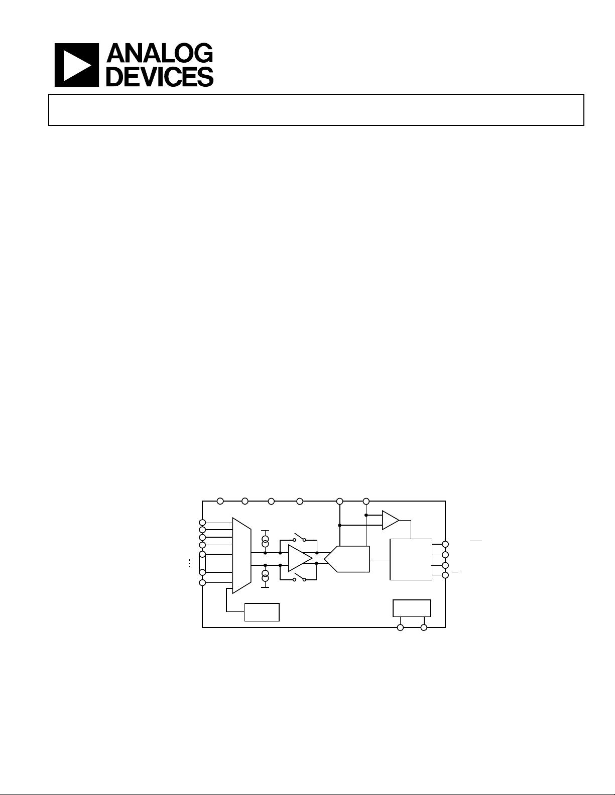
FUNCTIONAL BLOCK DIAGRAM
AVDDAGND
AIN1/P3
AIN2/P2
IN3/P1/REFIN2(+)
IN4/P0/REFIN2(–)
AIN5
AIN16
AINCOM
MUX
SENSOR
24-Bit Sigma-Delta ADC with PGA
Pressure measurement
Temperature measurement
Flow measurement
Weigh scales
Chromatography
Medical and scientific instrumentation
GENERAL DESCRIPTION
The AD7194 is a low noise, complete analog front end for high
precision measurement applications. It contains a low noise,
24-bit sigma-delta (Σ-) analog-to-digital converter (ADC).
The on-chip low noise gain stage means that signals of small
amplitude can interface directly to the ADC.
The device can be configured to have eight differential inputs or
sixteen pseudo differential inputs. The on-chip 4.92 MHz clock
can be used as the clock source to the ADC or, alternatively, an
external clock or crystal can be used. The output data rate from
the part can be varied from 4.7 Hz to 4.8 kHz.
The device has a very flexible digital filter, including a fast
settling option. Variables such as output data rate and settling
time are dependent on the option selected. For applications that
require all conversions to be settled, the AD7194 includes zero
latency.
The part operates with a power supply from 3 V to 5.25 V. It
consumes a current of 4.65 mA, and it is housed in a 32-lead
LFCSP package.
DVDDDGND REFIN1(+) REFIN1(–)
AV
AGND
TEMP
AD7194
DD
PGA
Σ-Δ
ADC
REFERENCE
DETECT
SERIAL
INTERFACE
AND
CONTROL
LOGIC
CLOCK
CIRCUITRY
AD7194
DOUT/RDY
DIN
SCLK
CS
MCLK1 MCLK2
Figure 1.
Rev. 0
Information furnished by Analog Devices is believed to be accurate and reliable. However, no
responsibility is assumed by Analog Devices for its use, nor for any infringements of patents or other
rights of third parties that may result from its use. Specifications subject to change without notice. No
license is granted by implication or otherwise under any patent or patent rights of Analog Devices.
Trademarks and registered trademarks are the property of their respective owners.
One Technology Way, P.O. Box 9106, Norwood, MA 02062-9106, U.S.A.
Tel: 781.329.4700 www.analog.com
Fax: 781.461.3113 ©2009 Analog Devices, Inc. All rights reserved.
8566-001

AD7194
TABLE OF CONTENTS
Features .............................................................................................. 1
Applications ....................................................................................... 1
General Description ......................................................................... 1
Functional Block Diagram .............................................................. 1
Revision History ............................................................................... 2
Specifications ..................................................................................... 3
Timing Characteristics ................................................................ 7
Absolute Maximum Ratings ............................................................ 9
Thermal Resistance ...................................................................... 9
ESD Caution .................................................................................. 9
Pin Configuration and Function Descriptions ........................... 10
Typical Performance Characteristics ........................................... 12
RMS Noise and Resolution ............................................................ 15
Sinc4 Chop Disabled ................................................................... 15
Sinc3 Chop Disabled ................................................................... 16
Fast Settling ................................................................................. 17
On-Chip Registers .......................................................................... 18
Communications Register ......................................................... 19
Status Register ............................................................................. 20
Mode Register ............................................................................. 21
Configuration Register .............................................................. 24
Data Register ............................................................................... 27
ID Register ................................................................................... 27
GPOCON Register ..................................................................... 27
Offset Register ............................................................................. 28
Full-Scale Register ...................................................................... 28
ADC Circuit Information .............................................................. 29
Overview ...................................................................................... 29
Analog Input Channel ............................................................... 30
Programmable Gain Array (PGA) ........................................... 30
Reference ..................................................................................... 30
Reference Detect ......................................................................... 31
Bipolar/Unipolar Configuration .............................................. 31
Data Output Coding .................................................................. 31
Burnout Currents ....................................................................... 31
Digital Interface .......................................................................... 32
Reset ............................................................................................. 36
System Synchronization ............................................................ 36
Enable Parity ............................................................................... 36
Clock ............................................................................................ 36
Temperature Sensor ................................................................... 36
Logic Outputs ............................................................................. 37
Calibration ................................................................................... 37
Digital Filter .................................................................................... 39
Sinc4 Filter (Chop Disabled) ..................................................... 39
Sinc3 Filter (Chop Disabled) ..................................................... 41
Chop Enabled (Sinc4 Filter) ...................................................... 43
Chop Enabled (Sinc3 Filter) ...................................................... 45
Fast Settling Mode (Sinc4 Filter) ............................................... 46
Fast Settling Mode (Sinc3 Filter) ............................................... 48
Fast Settling Mode (Chop Enabled) ......................................... 50
Summary of Filter Options ....................................................... 51
Grounding and Layout .................................................................. 52
Applications Information .............................................................. 53
Flowmeter .................................................................................... 53
Outline Dimensions ....................................................................... 54
Ordering Guide .......................................................................... 54
REVISION HISTORY
10/09—Revision 0: Initial Version
Rev. 0 | Page 2 of 56

AD7194
SPECIFICATIONS
AVDD = 3 V to 5.25 V, DVDD = 2.7 V to 5.25 V, AGND = DGND = 0 V; REFINx(+) = +2.5 V or AVDD, REFINx(−) = AGND,
MCLK = 4.92 MHz, T
Table 1.
Parameter Min Typ Max Unit Test Conditions/Comments1
ADC
Output Data Rate 4.7 4800 Hz Chop disabled
1.17 1200 Hz Chop enabled, sinc4 filter
1.56 1600 Hz Chop enabled, sinc3 filter
No Missing Codes2 24 Bits FS[9:0]3 > 1, sinc4 filter
24 Bits
Resolution See the RMS Noise and Resolution section
RMS Noise and Output
Data Rates
Integral Nonlinearity
Gain = 12 ±2 ±10 ppm of FSR AVDD = 5 V
±2 ±15 ppm of FSR AVDD = 3 V
Gain > 1 ±5 ±30 ppm of FSR AVDD = 5 V
±15 ±30 ppm of FSR AVDD = 3 V
Offset Error
±1 µV Chop enabled, AVDD = 5 V
±0.5 µV Chop enabled, AVDD = 3 V
Offset Error Drift vs.
±5 nV/°C Gain = 32 to 128; chop disabled
±5 nV/°C Chop enabled
Gain Error4 ±0.001 % AVDD = 5 V, gain = 1, TA = 25°C (factory
−0.4 % Gain = 128, before full-scale calibration
±0.003 % Gain > 1, after internal full-scale
±0.005 % Gain > 1, after internal full-scale
Gain Drift vs.
Power Supply Rejection 90 dB Gain = 1, VIN = 1 V
95 110 dB Gain > 1, VIN = 1 V/gain
Common-Mode Rejection
4, 5
±150/gain µV Chop disabled
Temperature
Temperature
@ DC 110 dB Gain = 1, VIN = 1 V
@ DC 105 120 dB Gain > 1, VIN = 1 V/gain
@ 50 Hz, 60 Hz2 120 dB 10 Hz output data rate, 50 Hz ± 1 Hz,
@ 50 Hz2 120 dB 50 Hz output data rate, 50 Hz ± 1 Hz
@ 60 Hz2 120 dB 60 Hz output data rate, 60 Hz ± 1 Hz
@ 50 Hz2 115 dB
@ 60 Hz2 115 dB
= T
A
to T
MIN
See the RMS Noise and Resolution section
±150/gain nV/°C Gain = 1 to 16; chop disabled
±1 ppm/°C
, unless otherwise noted.
MAX
3
> 4, sinc3 filter
FS[9:0]
calibration conditions)
(see Table 27)
calibration, AV
calibration, AV
60 Hz ± 1 Hz
Fast settling, FS[9:0]
50 Hz ± 1 Hz
Fast settling, FS[9:0]
60 Hz ± 1 Hz
≥ 4.75 V
DD
< 4.75 V
DD
3
3
= 6, average by 16,
= 5, average by 16,
Rev. 0 | Page 3 of 56

AD7194
Parameter Min Typ Max Unit Test Conditions/Comments1
Normal Mode Rejection2
Sinc4 Filter
Internal Clock
@ 50 Hz, 60 Hz 100 dB 10 Hz output data rate, 50 Hz ± 1 Hz,
74 dB 50 Hz output data rate, REJ606 = 1,
@ 50 Hz 96 dB 50 Hz output data rate, 50 Hz ± 1 Hz
@ 60 Hz 97 dB 60 Hz output data rate, 60 Hz ± 1 Hz
External Clock
@ 50 Hz, 60 Hz 120 dB 10 Hz output data rate, 50 Hz ± 1 Hz,
82 dB
@ 50 Hz 120 dB 50 Hz output data rate, 50 Hz ± 1 Hz
@ 60 Hz 120 dB 60 Hz output data rate, 60 Hz ± 1 Hz
Sinc3 Filter
Internal Clock
@ 50 Hz, 60 Hz 75 dB 10 Hz output data rate, 50 Hz ± 1 Hz,
60 dB 50 Hz output data rate, REJ606 = 1,
@ 50 Hz 70 dB 50 Hz output data rate, 50 Hz ± 1 Hz
@ 60 Hz 70 dB 60 Hz output data rate, 60 Hz ± 1 Hz
External Clock
@ 50 Hz, 60 Hz 100 dB 10 Hz output data rate, 50 Hz ± 1 Hz,
@ 50 Hz 67 dB 50 Hz output data rate, REJ606 = 1,
@ 50 Hz 95 dB 50 Hz output data rate, 50 Hz ± 1 Hz
@ 60 Hz 95 dB 60 Hz output data rate, 60 Hz ± 1 Hz
Fast Settling
Internal Clock
@ 50 Hz 26 dB
@ 60 Hz 26 dB
External Clock
@ 50 Hz 40 dB
@ 60 Hz 40 dB
ANALOG INPUTS
Differential Input
±V
/gain V VREF = REFINx(+) − REFINx(−),
REF
Voltage Ranges
−(AVDD − 1.25 V)/gain +(AVDD − 1.25 V)/gain V Gain > 1
Absolute AIN Voltage
2
Limits
Unbuffered Mode AGND − 0.05 AVDD + 0.05 V
Buffered Mode AGND + 0.25 AVDD − 0.25 V
Analog Input Current
Buffered Mode
Input Current2 −2 +2 nA Gain = 1
−3 +3 nA Gain > 1
Input Current Drift ±5 pA/°C
Unbuffered Mode
Input Current ±3.5 µA/V Gain = 1, input current varies with input
±1 µA/V Gain > 1
Input Current Drift ±0.05 nA/V/°C External clock
±1.6 nA/V/°C Internal clock
60 Hz ± 1 Hz
50 Hz ± 1 Hz, 60 Hz ± 1 Hz
60 Hz ± 1 Hz
50 Hz output data rate, REJ60
50 Hz ± 1 Hz, 60 Hz ± 1 Hz
60 Hz ± 1 Hz
50 Hz ± 1 Hz, 60 Hz ± 1 Hz
60 Hz ± 1 Hz
50 Hz ± 1 Hz, 60 Hz ± 1 Hz
3
= 6, average by 16, 50 Hz ± 0.5 Hz
FS[9:0]
3
= 5, average by 16, 60 Hz ± 0.5 Hz
FS[9:0]
3
= 6, average by 16, 50 Hz ± 0.5 Hz
FS[9:0]
3
= 5, average by 16, 60 Hz ± 0.5 Hz
FS[9:0]
gain = 1 to 128
voltage
6
= 1,
Rev. 0 | Page 4 of 56

AD7194
Parameter Min Typ Max Unit Test Conditions/Comments1
REFERENCE INPUT
REFIN Voltage 1 AVDD V REFIN = REFINx(+) − REFINx(−), the
Absolute REFIN Voltage
2
Limits
Average Reference Input
AGND − 0.05 AV
+ 0.05 V
DD
4.5 µA/V
Current
Average Reference Input
±0.03 nA/V/°C External clock
Current Drift
±1.3 nA/V/°C Internal clock
Normal Mode Rejection2 Same as for
analog inputs
Common-Mode
100 dB
Rejection
Reference Detect Levels 0.3 0.6 V
TEMPERATURE SENSOR
Accuracy ±2 °C Applies after user calibration at 25°C
Sensitivity 2815 Codes/°C Bipolar mode
BURNOUT CURRENTS
AIN Current 500 nA Analog inputs must be buffered and chop
DIGITAL OUTPUTS (P0 to P3)
Output High Voltage, VOH AVDD − 0.6 V AVDD = 3 V, I
4 V AVDD = 5 V, I
Output Low Voltage, VOL 0.4 V AVDD = 3 V, I
0.4 V AVDD = 5 V, I
Floating-State Leakage
Current
2
Floating-State Output
−100 +100 nA
10 pF
Capacitance
INTERNAL/EXTERNAL CLOCK
Internal Clock
Frequency 4.72 5.12 MHz
Duty Cycle 50:50 %
External Clock/Crystal
Frequency 2.4576 4.9152 5.12 MHz
Input Low Voltage, V
0.8 V DVDD = 5 V
INL
0.4 V DVDD = 3 V
Input High Voltage, V
2.5 V DVDD = 3 V
INH
3.5 V DVDD = 5 V
Input Current −10 +10 µA
LOGIC INPUTS
Input High Voltage, V
Input Low Voltage, V
2
2 V
INH
2
0.8 V
INL
Hysteresis2 0.1 0.25 V
Input Currents −10 +10 µA
LOGIC OUTPUT (DOUT/
Output High Voltage, V
RDY)
2
DVDD − 0.6 V DVDD = 3 V, I
OH
4 V DVDD = 5 V, I
Output Low Voltage, V
2
0.4 V DVDD = 3 V, I
OL
0.4 V DVDD = 5 V, I
Floating-State Leakage
−10 +10 µA
Current
Floating-State Output
10 pF
Capacitance
Data Output Coding Offset binary
differential input must be limited to
±(AV
− 1.25 V)/gain when gain > 1
DD
disabled
= 100 A
SOURCE
= 200 A
SOURCE
= 100 A
SINK
= 800 A
SINK
= 100 µA
SOURCE
= 200 µA
SOURCE
= 100 µA
SINK
= 1.6 mA
SINK
Rev. 0 | Page 5 of 56

AD7194
Parameter Min Typ Max Unit Test Conditions/Comments1
SYSTEM CALIBRATION2
Full-Scale Calibration Limit 1.05 × FS V
Zero-Scale Calibration
Limit
Input Span 0.8 × FS 2.1 × FS V
POWER REQUIREMENTS7
Power Supply Voltage
AVDD − AGND 3 5.25 V
DVDD − DGND 2.7 5.25 V
Power Supply Currents
AIDD Current 0.85 1.1 mA Gain = 1, buffer off
1 1.35 mA Gain = 1, buffer on
2.8 3.6 mA Gain = 8, buffer off
3.2 3.85 mA Gain = 8, buffer on
3.8 4.7 mA Gain = 16 to 128, buffer off
4.3 5.3 mA Gain = 16 to 128, buffer on
DIDD Current 0.35 0.4 mA DVDD = 3 V
0.5 0.6 mA DVDD = 5 V
1.5 mA External crystal used
IDD 3 µA Power-down mode
1
Temperature range: −40°C to +105°C.
2
Specification is not production tested, but is supported by characterization data at initial product release.
3
FS[9:0] is the decimal equivalent of Bit FS9 to Bit FS0 in the mode register.
4
Following a system or internal zero-scale calibration, the offset error is in the order of the noise for the programmed gain and output data rate selected. A system
full-scale calibration reduces the gain error to the order of the noise for the programmed gain and output data rate.
5
The analog inputs are configured for differential mode.
6
REJ60 is a bit in the mode register. When the first notch of the sinc filter is at 50 Hz, a notch is placed at 60 Hz when REJ60 is set to 1. This gives simultaneous
50 Hz/60 Hz rejection.
7
Digital inputs equal to DVDD or DGND.
−1.05 × FS V
Rev. 0 | Page 6 of 56
AD7194
TIMING CHARACTERISTICS
AVDD = 3 V to 5.25 V, DVDD = 2.7 V to 5.25 V, AGND = DGND = 0 V, Input Logic 0 = 0 V, Input Logic 1 = DVDD, unless otherwise noted.
Table 2.
Parameter Limit at T
MIN
, T
(B Version) Unit Conditions/Comments
MAX
1, 2
READ AND WRITE OPERATIONS
t3 100 ns min SCLK high pulse width
t4 100 ns min SCLK low pulse width
READ OPERATION
t1 0 ns min
falling edge to DOUT/RDY active time
CS
60 ns max DVDD = 4.75 V to 5.25 V
80 ns max DVDD = 2.7 V to 3.6 V
3
t
0 ns min SCLK active edge to data valid delay4
2
60 ns max DVDD = 4.75 V to 5.25 V
80 ns max DVDD = 2.7 V to 3.6 V
5, 6
t
10 ns min
5
Bus relinquish time after CS
inactive edge
80 ns max
t6 0 ns min
t7 10 ns min
SCLK inactive edge to CS
SCLK inactive edge to DOUT/RDY
inactive edge
high
WRITE OPERATION
t8 0 ns min
falling edge to SCLK active edge setup time4
CS
t9 30 ns min Data valid to SCLK edge setup time
t10 25 ns min Data valid to SCLK edge hold time
t11 0 ns min
1
Sample tested during initial release to ensure compliance. All input signals are specified with tR = tF = 5 ns (10% to 90% of DVDD) and timed from a voltage level of 1.6 V.
2
See Figure 3 and Figure 4.
3
These numbers are measured with the load circuit shown in Figure 2 and defined as the time required for the output to cross the VOL or VOH limits.
4
The SCLK active edge is the falling edge of SCLK.
5
These numbers are derived from the measured time taken by the data output to change 0.5 V when loaded with the circuit shown in Figure 2. The measured number
is then extrapolated back to remove the effects of charging or discharging the 50 pF capacitor. This means that the times quoted in the timing characteristics are the
true bus relinquish times of the part and, as such, are independent of external bus loading capacitances.
6
RDY
returns high after a read of the data register. In single conversion mode and continuous conversion mode, the same data can be read again, if required, while
is high, although care should be taken to ensure that subsequent reads do not occur close to the next output update. If the continuous read feature is enabled, the
digital word can be read only once.
rising edge to SCLK edge hold time
CS
RDY
Rev. 0 | Page 7 of 56
AD7194
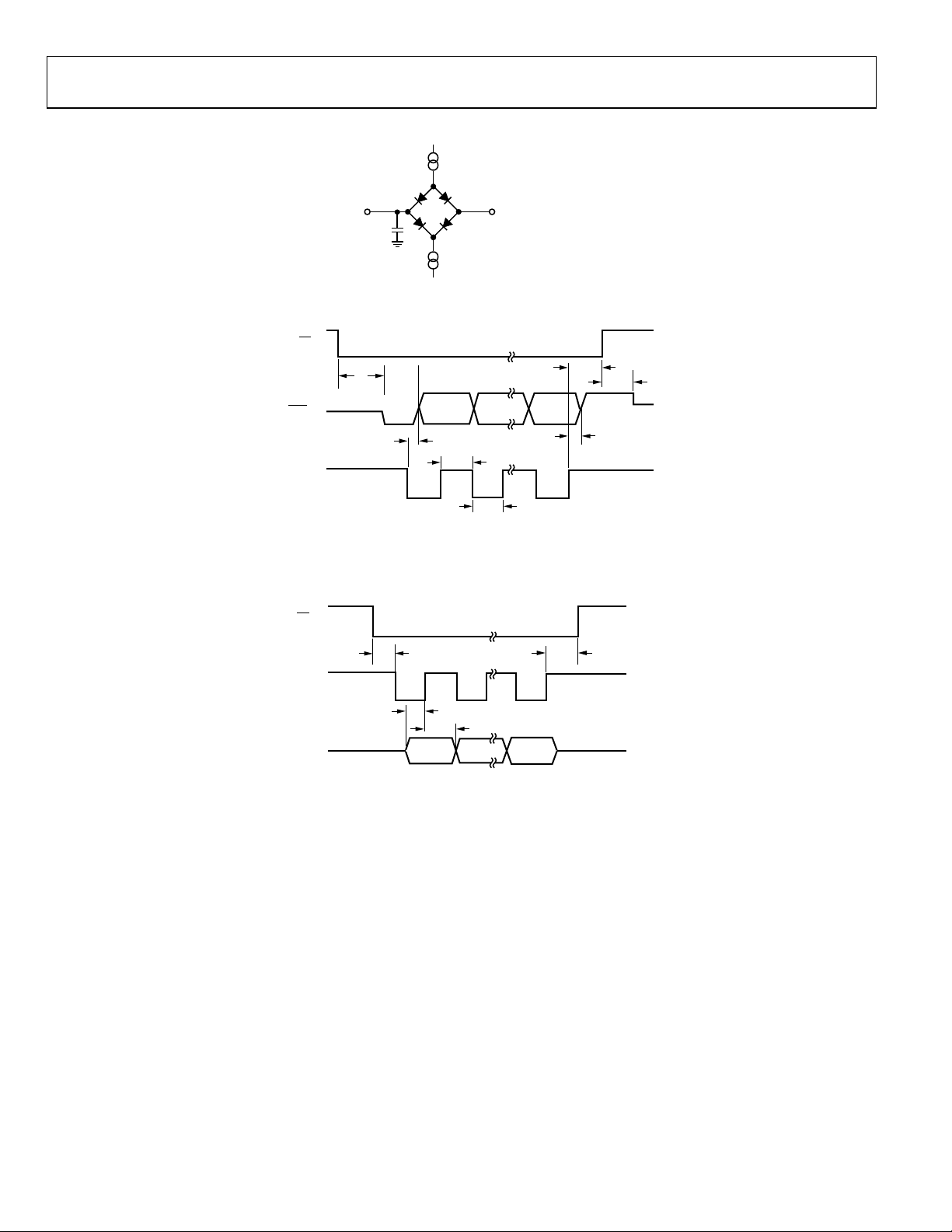
S
Circuit and Timing Diagrams
CS (I)
DOUT/RDY (O)
SCLK (I)
I
(1.6mA WITH DVDD = 5V,
SINK
TO
OUTPUT
PIN
50pF
100µA WIT H DV
I
SOURCE
100µA WIT H DV
= 3V)
DD
1.6V
(200µA WIT H DVDD = 5V,
= 3V)
DD
Figure 2. Load Circuit for Timing Characterization
t
1
MSB LSB
t
2
t
3
t
I = INPUT, O = OUTPUT
4
Figure 3. Read Cycle Timing Diagram
08566-002
t
6
t
5
t
7
08566-003
CS (I)
t
11
08566-004
CLK (I)
DIN (I)
I = INPUT, O = OUT PUT
t
8
t
9
t
10
MSB LSB
Figure 4. Write Cycle Timing Diagram
Rev. 0 | Page 8 of 56
AD7194
ABSOLUTE MAXIMUM RATINGS
TA = 25°C, unless otherwise noted.
Table 3.
Parameter Rating
AVDD to AGND −0.3 V to +6.5 V
DV
to AGND −0.3 V to +6.5 V
DD
AGND to DGND −0.3 V to +0.3 V
Analog Input Voltage to AGND −0.3 V to AVDD + 0.3 V
Reference Input Voltage to AGND −0.3 V to AVDD + 0.3 V
Digital Input Voltage to DGND −0.3 V to DVDD + 0.3 V
Digital Output Voltage to DGND −0.3 V to DVDD + 0.3 V
AINx/Digital Input Current 10 mA
Operating Temperature Range −40°C to +105°C
Storage Temperature Range −65°C to +150°C
Maximum Junction Temperature 150°C
Lead Temperature, Soldering Reflow 260°C
Stresses above those listed under Absolute Maximum Ratings
may cause permanent damage to the device. This is a stress
rating only; functional operation of the device at these or any
other conditions above those indicated in the operational
section of this specification is not implied. Exposure to absolute
maximum rating conditions for extended periods may affect
device reliability.
THERMAL RESISTANCE
θJA is specified for the worst-case conditions, that is, a device
soldered in a circuit board for surface-mount packages.
Table 4. Thermal Resistance
Package Type θJA θ
32-Lead LFCSP 32.5 32.71 °C/W
Unit
JC
ESD CAUTION
Rev. 0 | Page 9 of 56
AD7194
Y
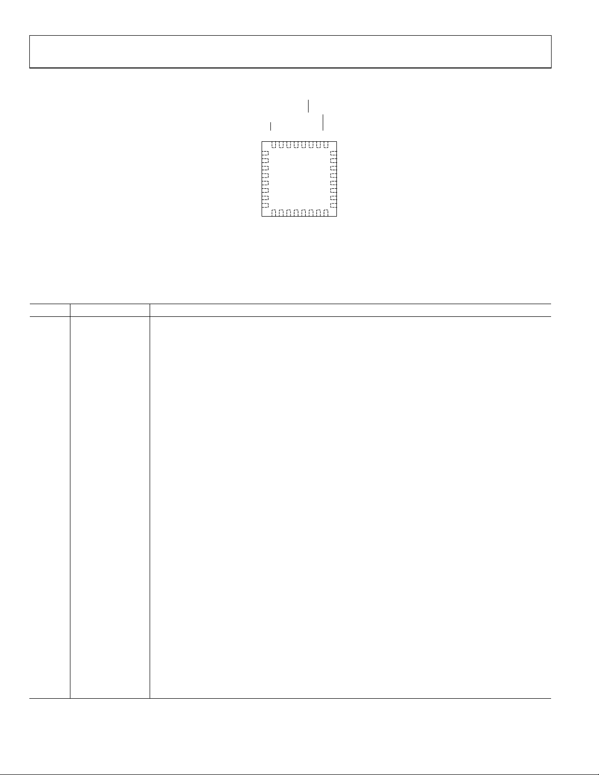
PIN CONFIGURATION AND FUNCTION DESCRIPTIONS
NC
CS
SCLK
MCLK2
MCLK1
32313029282726
AIN1/P3
1
2
AIN3/P1/REFIN2(+)
AIN4/P0/REFIN2(–)
NOTES
1. NC = NO CONNECT.
2. CONNECT EXP OSED PAD TO AGND.
AIN2/P2
AINCOM
AGND
AIN5
AIN6
3
4
5
6
7
8
AD7194
TOP VIEW
(Not to S cale)
9
10111213141516
AIN7
AIN8
AIN9
AIN10
Figure 5. Pin Configuration
Table 5. Pin Function Descriptions
Pin No. Mnemonic Description
1 AIN1/P3
Analog Input/Digital Output Pin. This pin can function as an analog input pin. When the GP32EN bit is set
to 1, the pin functions as a general-purpose output bit referenced between AV
2 AIN2/P2
Analog Input/Digital Output Pin. This pin can function as an analog input pin. When the GP32EN bit is set
to 1, the pin functions as a general-purpose output bit referenced between AVDD and AGND.
3 AIN3/P1/REFIN2(+)
Analog Input/Digital Output Pin/Positive Reference Input. This pin functions as an analog input pin. When
the GP10EN bit is set to 1, the pin functions as a general-purpose output bit referenced between AV
AGND. When the REFSEL bit in the configuration register is set to 1, this pin functions as REFIN2(+). An
external reference can be applied between REFIN2(+) and REFIN2(−). REFIN2(+) can lie anywhere between
AV
and AGND + 1 V.
DD
4 AIN4/P0/REFIN2(−)
Analog Input/Digital Output Pin/Positive Reference Input. This pin functions as an analog input pin. When
the GP10EN bit is set to 1, the pin functions as a general-purpose output bit referenced between AVDD and
AGND. When the REFSEL bit in the configuration register is set to 1, this pin functions as REFIN2(−). An
external reference can be applied between REFIN2(+) and REFIN2(−). This reference input can lie anywhere
between AGND and AV
DD
− 1 V.
5 AINCOM Analog Input AIN1 to Analog Input AIN16 are referenced to this input when the bit pseudo is set to 1.
6 AGND Analog Ground Reference Point.
7 AIN5 Analog Input Pin.
8 AIN6 Analog Input Pin.
9 AIN7 Analog Input Pin.
10 AIN8 Analog Input Pin.
11 AIN9 Analog Input Pin.
12 AIN10 Analog Input Pin.
13 AIN11 Analog Input Pin.
14 AIN12 Analog Input Pin.
15 AIN13 Analog Input Pin.
16 AIN14 Analog Input Pin.
17 REFIN1(+)
Positive Reference Input. An external reference can be applied between REFIN1(+) and REFIN1(−).
REFIN1(+) can lie anywhere between AV
REFIN1(−)), is AV
, but the part functions with a reference from 1 V to AVDD.
DD
18 REFIN1(−) Negative Reference Input. This reference input can lie anywhere between AGND and AVDD − 1 V.
19 AIN15 Analog Input Pin.
20 AIN16 Analog Input Pin.
21 AGND Analog Ground Reference Point.
22 DGND Digital Ground Reference Point.
SYNC
DIN
DOUT/RD
25
24 DV
DD
23
AV
DD
DGND
22
AGND
21
20
AIN16
19
AIN15
18
REFIN1(–)
17 REFIN1(+)
AIN11
AIN12
AIN13
AIN14
08566-005
and AGND.
DD
and AGND + 1 V. The nominal reference voltage, (REFIN1(+) −
DD
DD
and
Rev. 0 | Page 10 of 56

AD7194
Pin No. Mnemonic Description
23 AVDD
24 DVDD
25
SYNC
Logic input that allows for synchronization of the digital filters and analog modulators when using a
Analog Supply Voltage, 3 V to 5.25 V. AV
with AV
at 5 V or vice versa.
DD
Digital Supply Voltage, 2.7 V to 5.25 V. DV
with DV
at 5 V or vice versa.
DD
number of AD7194 devices. While SYNC
calibration control logic are reset, and the analog modulator is also held in its reset state. SYNC
affect the digital interface but does reset RDY
internally to DV
.
DD
26 NC This pin should be connected to GND for correct operation.
27
DOUT/RDY
Serial Data Output/Data Ready Output. DOUT/RDY serves a dual purpose. It functions as a serial data
output pin to access the output shift register of the ADC. The output shift register can contain data from
any of the on-chip data or control registers. In addition, DOUT/RDY
to indicate the completion of a conversion. If the data is not read after the conversion, the pin goes high
before the next update occurs. The DOUT/RDY
indicating that valid data is available. With an external serial clock, the data can be read using the
DOUT/RDY
pin. With CS low, the data-/control-word information is placed on the DOUT/RDY pin on the
SCLK falling edge and is valid on the SCLK rising edge.
28 DIN
Serial Data Input to the Input Shift Register on the ADC. Data in this shift register is transferred to the
control registers in the ADC, with the register selection bits of the communications register identifying the
appropriate register.
29 MCLK1
When the master clock for the device is provided externally by a crystal, the crystal is connected between
MCLK1 and MCLK2.
30 MCLK2
Master Clock Signal for the Device. The AD7194 has an internal 4.92 MHz clock. This internal clock can be
made available on the MCLK2 pin. The clock for the AD7194 can also be provided externally in the form of
a crystal or external clock. A crystal can be tied across the MCLK1 and MCLK2 pins. Alternatively, the MCLK2
pin can be driven with a CMOS-compatible clock and with the MCLK1 pin remaining unconnected.
31 SCLK
Serial Clock Input. This serial clock input is for data transfers to and from the ADC. The SCLK has a Schmitttriggered input, making the interface suitable for opto-isolated applications. The serial clock can be
continuous with all data transmitted in a continuous train of pulses. Alternatively, it can be a noncontinuous clock with the information transmitted to or from the ADC in smaller batches of data.
32
Chip Select Input. This is an active low logic input used to select the ADC. CS can be used to select the
CS
ADC in systems with more than one device on the serial bus or as a frame synchronization signal in
communicating with the device. CS
with SCLK, DIN, and DOUT used to interface with the device.
is independent of DVDD. Therefore, DVDD can be operated at 3 V
DD
is independent of AVDD. Therefore, AVDD can be operated at 3 V
DD
is low, the nodes of the digital filter, the filter control logic, and the
does not
to a high state if it is low. SYNC has a pull-up resistor
operates as a data ready pin, going low
falling edge can be used as an interrupt to a processor,
can be hardwired low, allowing the ADC to operate in 3-wire mode
Rev. 0 | Page 11 of 56
AD7194
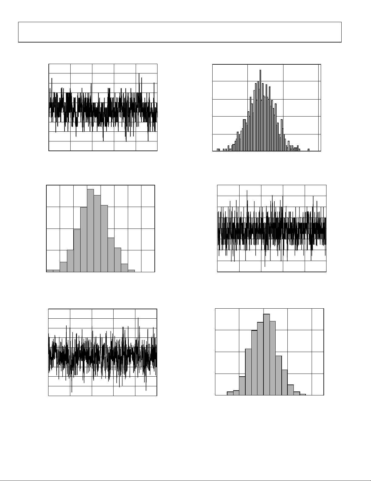
TYPICAL PERFORMANCE CHARACTERISTICS
8,387,952
8,387,950
8,387,948
8,387,946
8,387,944
CODE
8,387,942
8,387,940
8,387,938
8,387,936
8,387,934
0 200 400 600 800 1000
Figure 6. Noise (V
Gain = 128, Chop Disabled, Sinc
200
SAMPLE
= AVDD = 5 V, Output Data Rate = 4.7 Hz,
REF
4
Filter)
08566-006
50
40
30
20
OCCURRENCE
10
0
8,388,830 8,388,860 8,388,890 8,388,920
CODE
Figure 9. Noise Distribution Histogram (V
= AVDD = 5 V,
REF
Output Data Rate = 2400 Hz, Gain = 1, Chop Disabled, Sinc
8,388,880
8,388,878
4
Filter)
08566-009
150
100
OCCURRENCE
50
0
8,387,936
Figure 7. Noise Distribution Histogram (V
8,387,938
8,387,940
8,387,942
8,387,944
CODE
8,387,946
8,387,948
= AVDD = 5 V,
REF
Output Data Rate = 4.7 Hz, Gain = 128, Chop Disabled, Sinc
8,388,920
8,388,910
8,388,900
8,388,890
8,388,880
CODE
8,388,870
8,388,860
8,388,850
8,388,840
8,388,830
0 200 400 600 800 1000
SAMPLE
Figure 8. Noise (V
= AVDD = 5 V, Output Data Rate = 2400 Hz,
REF
Gain = 1, Chop Disabled, Sinc
4
Filter)
8,387,950
4
Filter)
8,388,876
8,388,874
8,388,872
CODE
8,388,870
8,388,868
8,388,866
8,388,864
0 200 400 600 800 1000
8566-007
Figure 10. Noise (V
= AVDD = 5 V, Output Data Rate = 42.1 Hz (FS[9:0] = 6,
REF
Average by 16), Gain = 1, Chop Disabled, Sinc
200
150
100
OCCURRENCE
50
0
8,388,864 8,388,868 8,388,872 8,388,876 8,388,880
08566-008
Figu re 11. Noise Distribution Histogram (V
SAMPLE
4
Filter)
CODE
= AVDD = 5 V, Output Data Rate =
REF
42.1 Hz (FS[9:0] = 6, Average by 16), Gain = 1, Chop Disabled, Sinc
4
Filter)
08566-010
08566-011
Rev. 0 | Page 12 of 56
AD7194
5
0.6
4
3
2
1
INL (ppm of FSR)
0
–1
–2
–4–3–2–101234
VIN (V)
Figure 12. INL (Gain = 1)
20
15
10
5
0
–5
INL (ppm of FSR)
–10
–15
–20
–0.03 –0.02 –0.01 0 0.01 0.02 0.03
VIN (V)
Figure 13. INL (Gain = 128)
0.5
0.4
0.3
0.2
OFFSET ERROR (μV)
0.1
0
–60 –40 –20 0 20 40 60 80 100 120
08566-012
TEMPERAUTRE (°C)
08566-067
Figure 15. Offset vs. Temperature (Gain = 128, Chop Disabled)
1.000008
1.000006
1.000004
1.000002
1.000000
0.999998
GAIN
0.999996
0.999994
0.999992
0.999990
0.999988
–60 –40 –20 0 20 40 60 80 100 120
08566-013
TEMPERATURE (°C)
08566-016
Figure 16. Gain vs. Temperature (Gain = 1)
170
168
166
164
162
OFFSET (µV)
160
158
156
154
–60 –40 –20 0 20 40 60 80 100 120
TEMPERATURE ( °C)
Figure 14. Offset vs. Temperature (Gain = 1, Chop Disabled)
08566-014
Rev. 0 | Page 13 of 56
128.004
128.002
128.000
127.998
127.996
GAIN
127.994
127.992
127.990
127.988
–60 –40 –20 0 20 40 60 80 100 120
TEMPERATURE (°C)
Figure 17. Gain vs. Temperature (Gain = 128)
08566-017
AD7194
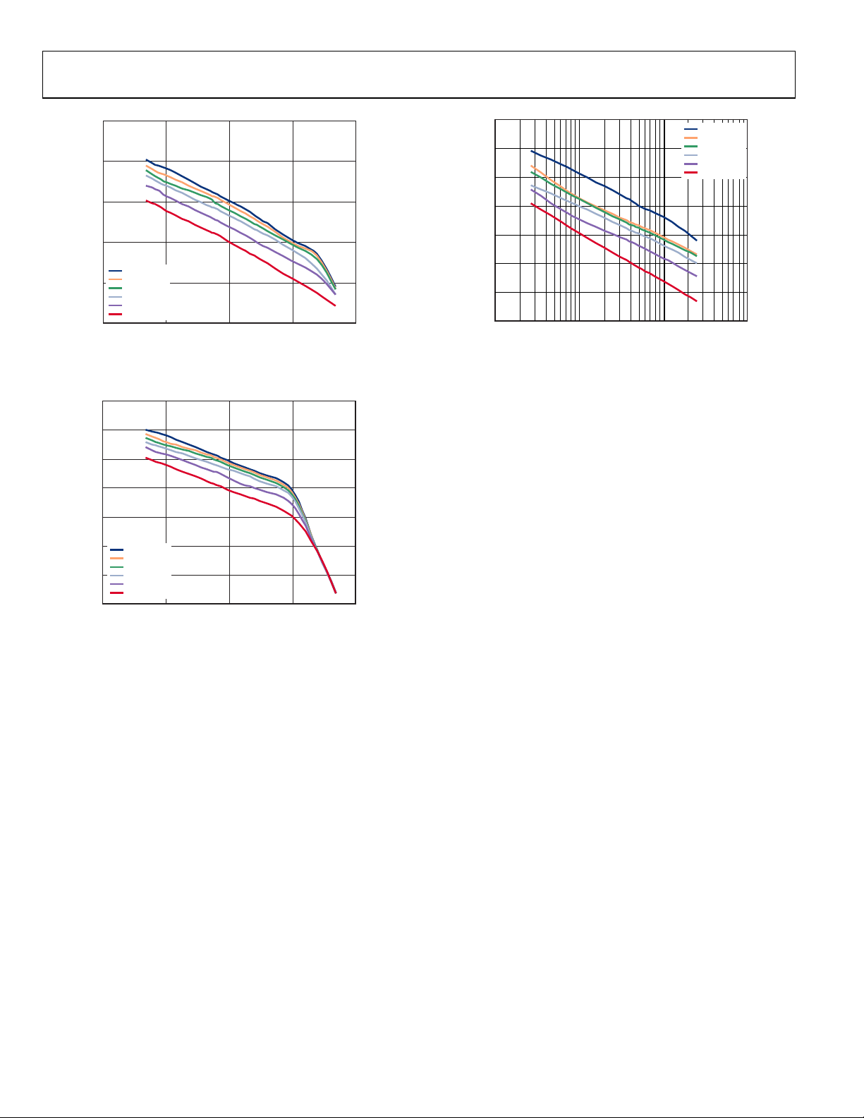
24
22
20
23
22
21
20
GAIN = 1
GAIN = 8
GAIN = 16
GAIN = 32
GAIN = 64
GAIN = 128
18
GAIN = 1
GAIN = 8
16
NOISE FREE RESOL UTION (Bits)
Figure 18. Noise-Free Resolution (Sinc
GAIN = 16
GAIN = 32
GAIN = 64
GAIN = 128
14
1 10 100 1k 10k
OUTPUT DATA RAT E (Hz)
4
Filter, Chop Disabled, V
24
22
20
18
16
14
GAIN = 1
NOISE FREE RESOLUTION (Bits)
GAIN = 8
GAIN = 16
12
GAIN = 32
GAIN = 64
GAIN = 128
10
1 10 100 1k 10k
OUTPUT DATA RATE (Hz)
Figure 19. Noise-Free Resolution (Sinc3 Filter, Chop Disabled, V
REF
REF
= 5 V)
= 5 V)
19
18
NOISE FREE RESOLUTION (Bits)
17
16
1 10 100 1k
08566-069
Figure 20. Noise-Free Resolution in Fast Settling Mode (V
Averaging by 16, Sinc
OUTPUT DATA RATE (Hz)
4
Filter, Chop Disabled)
REF
08566-068
= 5 V,
08566-070
Rev. 0 | Page 14 of 56
AD7194
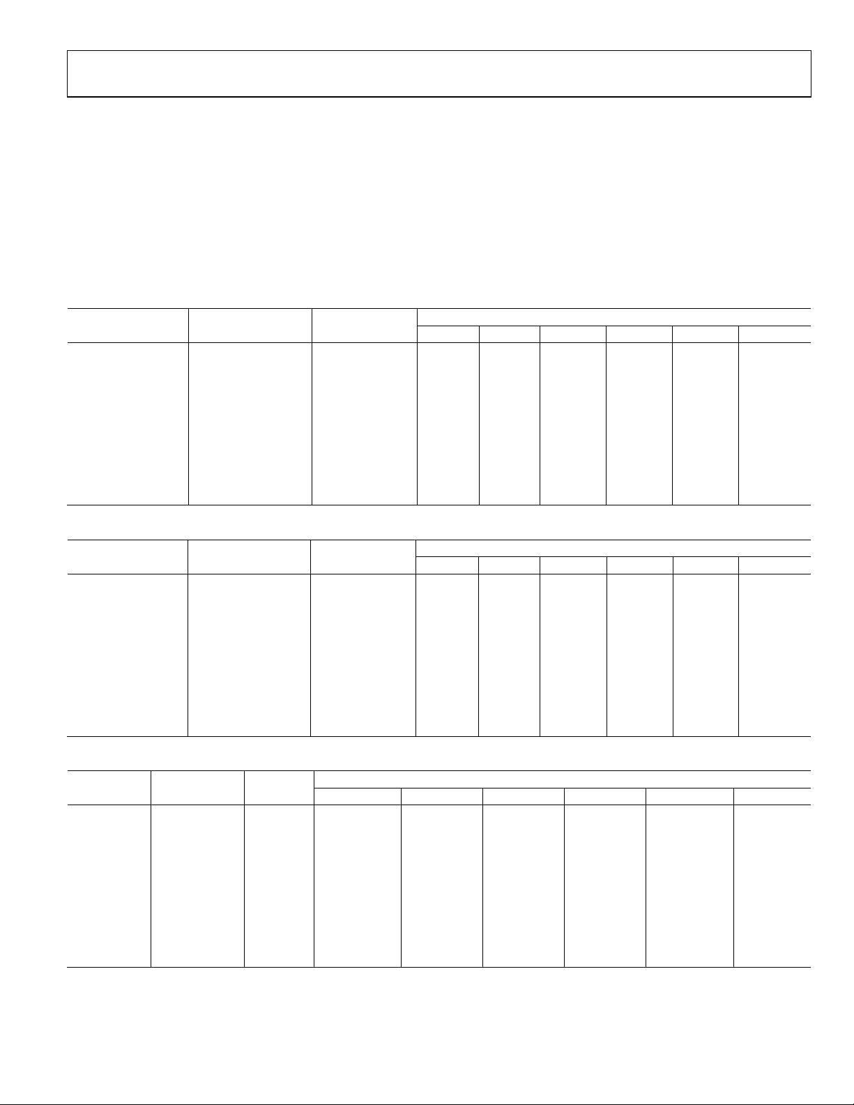
RMS NOISE AND RESOLUTION
The following tables show the rms noise, peak-to-peak noise,
effective resolution, and noise-free (peak-to-peak) resolution of
the AD7194 for various output data rates and gain settings with
chop disabled for the sinc
4
and sinc3 filters and for fast settling
mode. The numbers given are for the bipolar input range with
an external 5 V reference. These numbers are typical and are
generated with a differential input voltage of 0 V when the ADC
SINC4 CHOP DISABLED
Table 6. RMS Noise (nV) vs. Gain and Output Data Rate
Filter Word
(Decimal)
1023 4.7 852.5 370 57 35 18 13 11
640 7.5 533 440 73 41 24 17 13
480 10 400 470 83 45 28 18 16
96 50 80 1100 150 85 52 38 34
80 60 66.7 1200 170 94 56 42 38
32 150 26.7 1800 260 150 86 65 59
16 300 13.3 2500 360 210 130 95 83
5 960 4.17 4500 640 370 230 170 150
2 2400 1.67 7500 1100 600 380 280 240
1 4800 0.83 26,000 3400 1800 940 550 390
Output Data
Rate (Hz)
Settling
Time (ms)
is continuously converting on a single channel. It is important
to note that the effective resolution is calculated using the rms
noise, whereas the peak-to-peak resolution is calculated based
on peak-to-peak noise. The peak-to-peak resolution represents
the resolution for which there is no code flicker. With chop
enabled, the resolution improves by 0.5 bits.
Gain of
1 8 16 32 64 128
Table 7. Peak-to-Peak Noise (nV) vs. Gain and Output Data Rate
Filter Word
(Decimal)
1023 4.7 852.5 2200 340 200 120 84 70
640 7.5 533 2700 430 260 150 100 85
480 10 400 3000 480 300 170 120 100
96 50 80 6600 950 540 350 250 210
80 60 66.7 7200 1000 610 370 270 220
32 150 26.7 11,000 1600 970 580 430 370
16 300 13.3 17,000 2400 1400 840 620 530
5 960 4.17 35,000 4800 2500 1500 1100 1000
2 2400 1.67 56,000 7500 4200 2900 1800 1700
1 4800 0.83 175,000 23,000 12,000 7100 3600 2600
Output Data
Rate (Hz)
Settling
Time (ms)
1 8 16 32 64 128
Gain of
Table 8. Effective Resolution (Peak-to-Peak Resolution) vs. Gain and Output Data Rate
1
Filter Word
(Decimal)
1023 4.7 852.5 24 (22.1) 24 (21.8) 24 (21.6) 24 (21.3) 23.5 (20.8) 22.8 (20.1)
640 7.5 533 24 (21.8) 24 (21.5) 23.9 (21.2) 23.6 (21) 23.1 (20.6) 22.5 (19.8)
480 10 400 24 (21.7) 24 (21.3) 23.7 (21) 23.4 (20.8) 23 (20.3) 22.2 (19.6)
96 50 80 23.1 (20.5) 23 (20.3) 22.8 (20.1) 22.5 (19.8) 22 (19.3) 21.1 (18.5)
80 60 66.7 23 (20.4) 22.9 (20.3) 22.7 (20) 22.4 (19.7) 21.8 (19.1) 21 (18.4)
32 150 26.7 22.4 (19.8) 22.3 (19.6) 22 (19.3) 21.8 (19) 21.2 (18.5) 20.3 (17.7)
16 300 13.3 21.9 (19.2) 21.8 (19) 21.5 (18.8) 21.2 (18.5) 20.7 (17.9) 19.8 (17.2)
5 960 4.17 21.1 (18.4) 21 (18) 20.7 (17.9) 20.4 (17.7) 19.8 (17.1) 19 (16.3)
2 2400 1.67 20.4 (17.6) 20.3 (17.3) 20 (17.2) 19.6 (16.7) 19.1 (16.4) 18.3 (15.5)
1 4800 0.83 18.6 (15.8) 18.5 (15.7) 18.4 (15.7) 18.3 (15.4) 18.1 (15.4) 17.6 (14.9)
1
The output peak-to-peak (p-p) resolution is listed in parentheses.
Output Data
Rate (Hz)
Settling
Time (ms)
1 8 16 32 64 128
Gain of
Rev. 0 | Page 15 of 56
AD7194
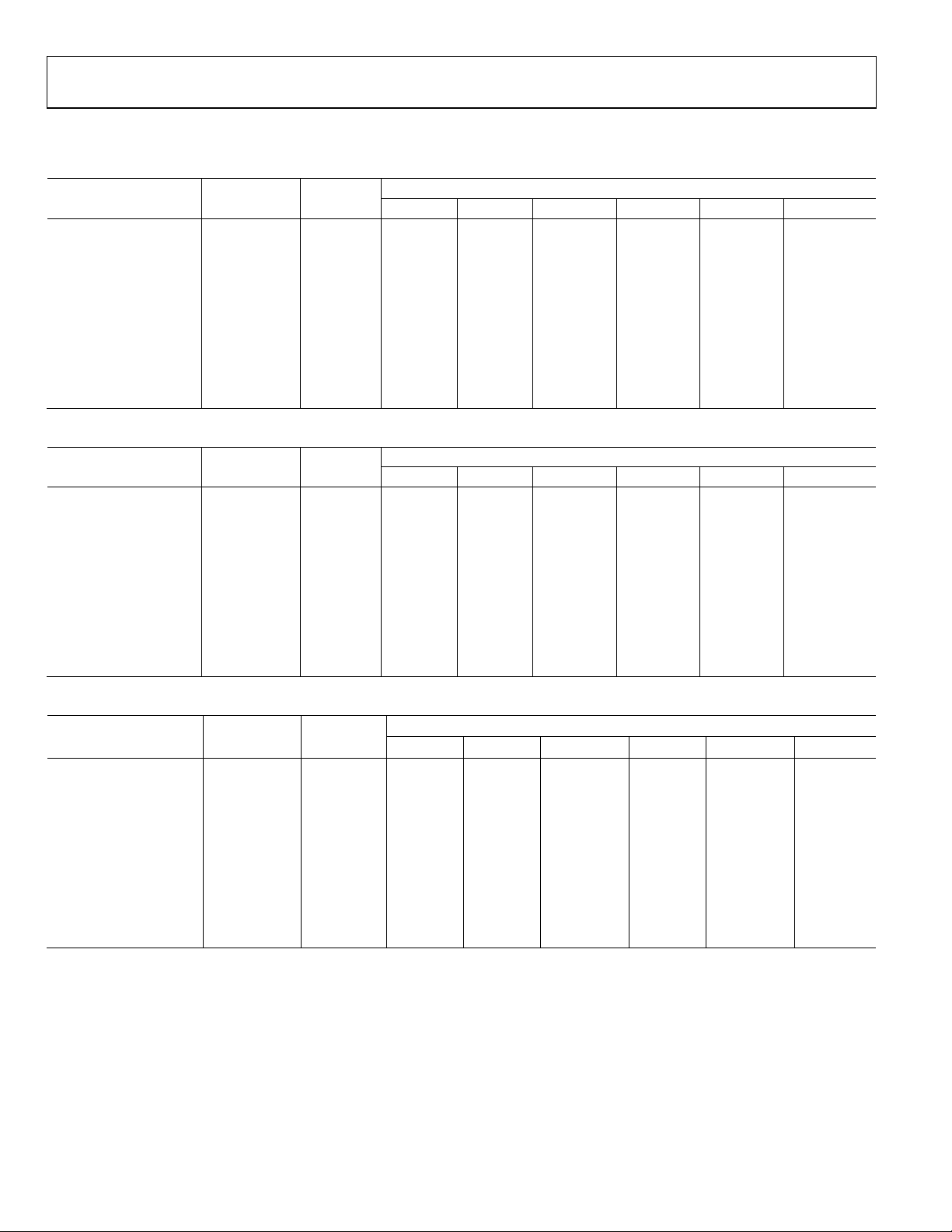
SINC3 CHOP DISABLED
Table 9. RMS Noise (nV) vs. Gain and Output Data Rate
Output Data
Filter Word (Decimal)
1023 4.7 639.4 380 58 35 20 13 11
640 7.5 400 450 73 41 25 17 14
480 10 300 490 90 47 28 19 16
96 50 60 1100 160 92 54 40 36
80 60 50 1200 170 99 59 43 39
32 150 20 1900 280 160 91 72 63
16 300 10 2700 380 210 130 97 87
5 960 3.13 6400 870 490 280 200 170
2 2400 1.25 115,000 14,000 7000 3600 1800 950
1 4800 0.625 860,000 110,000 54,000 28,000 14,000 7000
Rate (Hz)
Settling
Time (ms)
1 8 16 32 64 128
Table 10. Peak-to-Peak Noise (nV) vs. Gain and Output Data Rate
Output Data
Filter Word (Decimal)
1023 4.7 639.4 2300 350 220 130 84 70
640 7.5 400 2700 450 270 160 110 88
480 10 300 3100 520 310 180 120 100
96 50 60 7200 990 560 370 260 230
80 60 50 7800 1100 630 390 270 250
32 150 20 13,000 1800 1000 580 480 400
16 300 10 19,000 2500 1400 860 640 560
5 960 3.13 410,000 5700 3200 1800 1300 1100
2 2400 1.25 730,000 93,000 47,000 24,000 12,000 6100
1 4800 0.625 5,700,000 730,000 360,000 180,000 93,000 45,000
Rate (Hz)
Settling
Time (ms)
1 8 16 32 64 128
Gain of
Gain of
Table 11. Effective Resolution (Peak-to-Peak Resolution) vs. Gain and Output Data Rate
Output Data
Filter Word (Decimal)
1023 4.7 639.4 24 (22.1) 24 (21.8) 24 (21.4) 23.9 (21.2) 23.5 (20.8) 22.8 (20.1)
640 7.5 400 24 (21.8) 24 (21.4) 23.9 (21.1) 23.6 (20.9) 23.1 (20.4) 22.4 (19.8)
480 10 300 24 (21.6) 23.8 (21.2) 23.7 (20.9) 23.4 (20.7) 23 (20.3) 22.2 (19.6)
96 50 60 23.1 (20.4) 22.9 (20.3) 22.7 (20.1) 22.5 (19.7) 21.9 (19.2) 21 (18.4)
80 60 50 23 (20.3) 22.8 (20.1) 22.6 (19.9) 22.3 (19.6) 21.8 (19.1) 20.9 (18.3)
32 150 20 22.3 (19.6) 22.1 (19.4) 21.9 (19.3) 21.7 (19) 21 (18.3) 20.2 (17.6)
16 300 10 21.8 (19) 21.6 (18.9) 21.56 (18.8) 21.2 (18.5) 20.6 (17.9) 19.8 (17.1)
5 960 3.13 20.6 (17.9) 20.5 (17.7) 20.3 (17.6) 20.1 (17.4) 19.6 (16.9) 18.8 (16.1)
2 2400 1.25 16.5 (13.7) 16.4 (13.7) 16.4 (13.7) 16.4 (13.7) 16.4 (13.7) 16.4 (13.6)
1 4800 0.625 13.5 (10.8) 13.5 (10.7) 13.5 (10.7) 13.5 (10.7) 13.5 (10.7) 13.5 (10.7)
1
The output peak-to-peak (p-p) resolution is listed in parentheses.
Rate (Hz)
Settling
Time (ms)
1 8 16 32 64 128
Gain of1
Rev. 0 | Page 16 of 56
AD7194
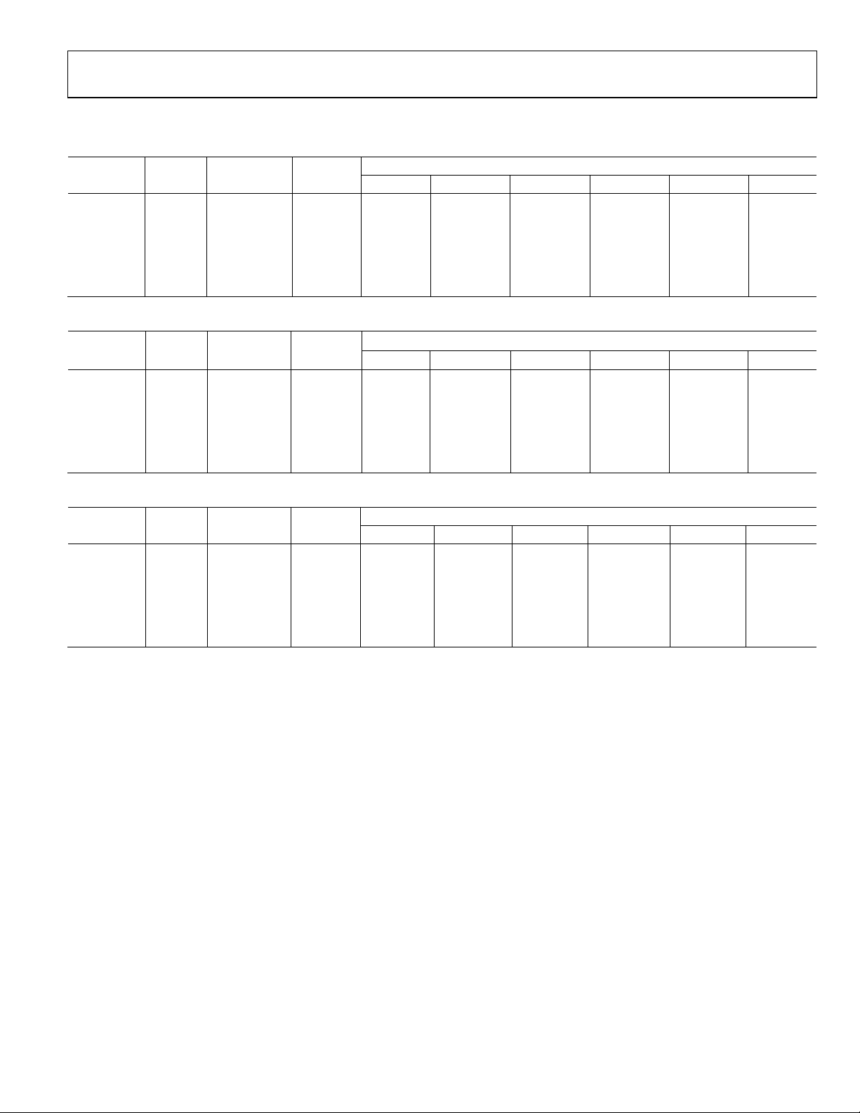
FAST SETTLING
Table 12. RMS Noise (nV) vs. Gain and Output Data Rate
Filter Wo rd
(Decimal)
96 16 2.63 380 410 87 52 33 15 12
30 16 8.4 118.75 700 140 71 43 30 21
6 16 42.10 23.75 1500 270 150 82 56 47
5 16 50.53 19.79 1600 280 160 88 61 52
2 16 126.32 7.92 2700 380 210 130 94 85
1 16 252.63 3.96 3700 540 300 190 140 120
Average
Output Data
Rate (Hz)
Settling
Time (ms)
1 8 16 32 64 128
Table 13. Peak-to-Peak Noise (nV) vs. Gain and Output Data Rate
Filter Wo rd
(Decimal) Average
96 16 2.63 380 2500 450 260 180 100 70
30 16 8.4 118.75 4200 900 470 280 190 130
6 16 42.10 23.75 10,000 1800 950 540 360 300
5 16 50.53 19.79 11,000 1900 1000 580 390 330
2 16 126.32 7.92 16,000 2800 1500 850 580 510
1 16 252.63 3.96 23,000 4500 2000 1200 850 740
Output Data
Rate (Hz)
Settling
Time (ms)
1 8 16 32 64 128
Gain of
Gain of
Table 14. Effective Resolution (Peak-to-Peak Resolution) vs. Gain and Output Data Rate
Filter Wo rd
(Decimal) Average
96 16 2.63 380 24 (21.9) 23.8 (21.4) 23.5 (21.2) 23.2 (20.7) 23.3 (20.6) 22.6 (20.1)
30 16 8.4 118.75 23.8 (21.2) 23.1 (20.4) 23.1 (20.3) 22.8 (20.1) 22.3 (19.6) 21.8 (19.2)
6 16 42.10 23.75 22.7 (19.9) 22.1 (19.4) 22 (19.3) 21.9 (19.1) 21.4 (18.7) 20.7 (18)
5 16 50.53 19.79 22.6 (19.8) 22.1 (19.3) 21.9 (19.3) 21.8 (19) 21.3 (18.6) 20.5 (17.9)
2 16 126.32 7.92 21.8 (19.3) 21.6 (18.8) 21.5 (18.7) 21.2 (18.5) 20.7 (18) 19.8 (17.2)
1 16 252.63 3.96 21.4 (18.7) 21.1 (18.1) 21 (18.3) 20.6 (18) 20.1 (17.5) 19.3 (16.7)
1
The output peak-to-peak (p-p) resolution is listed in parentheses.
Output Data
Rate (Hz)
Settling
Time (ms)
1 8 16 32 64 128
Gain of1
Rev. 0 | Page 17 of 56

AD7194
ON-CHIP REGISTERS
The ADC is controlled and configured via a number of on-chip registers that are described on the following pages wherein the term, set,
implies a Logic 1 state and cleared implies a Logic 0 state, unless otherwise noted.
Table 15. Register Summary
Register Addr. Dir. Default Bit 7 Bit 6 Bit 5 Bit 4 Bit 3 Bit 2 Bit 1 Bit 0
Communications 00 W 00 0
Status 00 R 80
Mode 01 R/W 080060 Mode select DAT_STA CLK1 CLK0 AVG1 AVG0
SINC3 0 ENPAR CLK_DIV Single REJ60 FS9 FS8
FS7 FS6 FS5 FS4 FS3 FS2 FS1 FS0 (LSB)
Configuration 02 R/W 000117 Chop (MSB) 0 0 REFSEL 0 Pseudo 0 TEMP
CH7( CH6 CH5 CH4 CH3 CH2 CH1 CH0
Burn REFDET 0 BUF
Data 03 R 000000 D23 (MSB) D22 D21 D20 D19 D18 D17 D16
D15 D14 D13 D12 D11 D10 D9 D8
D7 D6 D5 D4 D3 D2 D1 D0 (LSB)
ID 04 R X3 X X X X 0 0 1 1
GPOCON 05 R/W 00 0 0 GP32EN GP10EN P3DAT P2DAT P1DAT P0DAT
Offset 06 R/W 800000 OF23 (MSB) OF22 OF21 OF20 OF19 OF18 OF17 OF16
OF15 OF14 OF13 OF12 OF11 OF10 OF9 OF8
OF7 OF6 OF5 OF4 OF3 OF2 OF1 OF0 (LSB)
Full Scale 07 R/W 5XXXX0 FS23 (MSB) FS22 FS21 FS20 FS19 FS18 FS17 FS16
FS15 FS14 FS13 FS12 FS11 FS10 FS9 FS8
FS7 FS6 FS5 FS4 FS3 FS2 FS1 FS0 (LSB)
RDY
R/W
ERR NOREF Parity CHD3 CHD2 CHD1 CHD0
Register address
U/B
CREAD 0 0
G2 G1 G0 (LSB)
Rev. 0 | Page 18 of 56

AD7194
COMMUNICATIONS REGISTER
RS2, RS1, RS0 = 000
The communications register is an 8-bit write-only register. All
communications to the part must start with a write operation to
the communications register. The data written to the communications register determine whether the next operation is a read
or write operation and in which register this operation occurs. For
read or write operations, when the subsequent read or write operation to the selected register is complete, the interface returns to
where it expects a write operation to the communications register.
This is the default state of the interface and, on power-up or after
CR7 CR6 CR5 CR4 CR3 CR2 CR1 CR0
WEN(0) R/W(0)
Table 16. Communications Register (CR) Bit Designations
Bit Location Bit Name Description
CR7
CR6
1 in this bit position indicates that the next operation is a read from the designated register.
CR5 to CR3 RS2 to RS0
CR2 CREAD
CR1 to CR0 0 These bits must be programmed to Logic 0 for correct operation.
Write enable bit. For a write to the communications register to occur, 0 must be written to this bit. If a 1 is
WEN
R/W
RS2(0) RS1(0) RS0(0) CREAD(0) 0(0) 0(0)
the first bit written, the part does not clock onto subsequent bits in the register; rather, it stays at this bit
location until a 0 is written to this bit. After a 0 is written to the WEN
the communications register. Idling the DIN pin high between data transfers minimizes the effects of
spurious SCLK pulses on the serial interface.
0 in this bit location indicates that the next operation is a write to a specified register.
Register address bits. These address bits are used to select which registers of the ADC are selected during
the serial interface communication (see Tabl e 17).
Continuous read of the data register. When this bit is set to 1 (and the data register is selected), the serial
interface is configured so that the data register can be continuously read; that is, the contents of the data
register are automatically placed on the DOUT pin when the SCLK pulses are applied after the RDY
goes low to indicate that a conversion is complete. The communications register does not have to be
written to for subsequent data reads. To enable continuous read, Instruction 01011100 must be written to
the communications register. To disable continuous read, Instruction 01011000 must be written to the
communications register while the RDY
activity on the DIN line so that it can receive the instruction to disable continuous read. Additionally, a
reset occurs if 40 consecutive 1s occur on DIN; therefore, hold DIN low until an instruction is written to
the device.
a reset, the ADC is in this default state waiting for a write
operation to the communications register. In situations where the
interface sequence is lost, a write operation of at least 40 serial
clock cycles with DIN high returns the ADC to this default state
by resetting the entire part. Tab le 1 6 outlines the bit designations
for the communications register. CR0 through CR7 indicate the
bit location, CR denoting that the bits are in the communications
register. CR7 denotes the first bit of the data stream. The number
in parentheses indicates the power-on/reset default status of
that bit.
bit, the next seven bits are loaded to
pin
pin is low. While continuous read is enabled, the ADC monitors
Table 17. Register Selection
RS2 RS1 RS0 Register Register Size
0 0 0 Communications register during a write operation 8 bits
0 0 0 Status register during a read operation 8 bits
0 0 1 Mode register 24 bits
0 1 0 Configuration register 24 bits
0 1 1 Data register/data register plus status information 24 bits/32 bits
1 0 0 ID register 8 bits
1 0 1 GPOCON register 8 bits
1 1 0 Offset register 24 bits
1 1 1 Full-scale register 24 bits
Rev. 0 | Page 19 of 56

AD7194
STATUS REGISTER
RS2, RS1, RS0 = 000; Power-On/Reset = 0x80
The status register is an 8-bit read-only register. To access the
ADC status register, the user must write to the communications
register, select the next operation to be a read operation, and
SR7 SR6 SR5 SR4 SR3 SR2 SR1 SR0
RDY(1)
Table 18. Status Register (SR) Bit Designations
Bit Location Bit Name Description
SR7
SR6 ERR
SR5 NOREF
SR4 Parity
SR3 to SR0 CHD3 to CHD0
ERR(0) NOREF(0) Parity(0) CHD3(0) CHD2(0) CHD1(0) CHD0(0)
Ready bit for the ADC. This bit is cleared when data is written to the ADC data register. The RDY bit is set
RDY
automatically after the ADC data register is read, or a period of time before the data register is updated,
with a new conversion result to indicate to the user that the conversion data should not be read. It is
also set when the part is placed in power-down mode or idle mode or when SYNC
of a conversion is also indicated by the DOUT/RDY
status register for monitoring the ADC for conversion data.
ADC error bit. This bit is written to at the same time as the RDY
result written to the ADC data register is clamped to all 0s or all 1s. Error sources include overrange,
underrange, or the absence of a reference voltage. This bit is cleared when the result written to the data
register returns to within the allowed analog input range. The ERR bit is also set during calibrations if
the reference source is invalid or if the applied analog input voltages are outside range during system
calibrations.
No external reference bit. This bit is set to indicate that the selected reference (REFIN1 or REFIN2) is at a
voltage that is below a specified threshold. When set, conversion results are clamped to all 1s. This bit is
cleared to indicate that a valid reference is applied to the selected reference pins. The NOREF bit is enabled
by setting the REFDET bit in the configuration register to 1.
Parity check of the data register. If the ENPAR bit in the mode register is set, the parity bit is set if there is
an odd number of 1s in the data register. It is cleared if there is an even number of 1s in the data
register. The DAT_STA bit in the mode register should be set when the parity check is used. When the
DAT_STA bit is set, the contents of the status register are transmitted along with the data for each data
register read.
These bits indicate which channel corresponds to the data register contents. They do not indicate
which channel is presently being converted, but indicate which channel was selected when the
conversion contained in the data register was generated.
load Bit RS2, Bit RS1, and Bit RS0 with 0. Tabl e 1 8 outlines the bit
designations for the status register. SR0 through SR7 indicate the
bit locations, SR denoting that the bits are in the status register.
SR7 denotes the first bit of the data stream. The number in parentheses indicates the power-on/reset default status of that bit.
is taken low. The end
pin. This pin can be used as an alternative to the
bit. This bit is set to indicate that the
Rev. 0 | Page 20 of 56

AD7194
MODE REGISTER
RS2, RS1, RS0 = 001; Power-On/Reset = 0x080060
The mode register is a 24-bit register from which data can be
read or to which data can be written. This register is used to
select the operating mode, the output data rate, and the clock
source. Tabl e 19 outlines the bit designations for the mode
MR23 MR22 MR21 MR20 MR19 MR18 MR17 MR16
MD2(0) MD1(0) MD0(0) DAT_STA(0) CLK1(1) CLK0(0) AVG1(0) AVG0(0)
MR15 MR14 MR13 MR12 MR11 MR10 MR9 MR8
SINC3(0) 0 ENPAR(0) CLK_DIV(0) Single(0) REJ60(0) FS9(0) FS8(0)
MR7 MR6 MR5 MR4 MR3 MR2 MR1 MR0
FS7(0) FS6(1) FS5(1) FS4(0) FS3(0) FS2(0) FS1(0) FS0(0)
Table 19. Mode Register (MR) Bit Designations
Bit Location Bit Name Description
MR23 to
MR21
MR20 DAT_STA
MR19, MR18 CLK1, CLK0
MR17, MR16 AVG1, AVG0
0 0 No averaging (fast settling mode disabled)
0 1 Average by 2
1 0 Average by 8
1 1 Average by 16
MR15 SINC3
MR14 0 This bit must be programmed with a Logic 0 for correct operation.
MR13 ENPAR
MD2 to MD0 Mode select bits. These bits select the operating mode of the AD7194 (see Table 20).
This bit enables the transmission of status register contents after each data register read. When DAT_STA
is set, the contents of the status register are transmitted along with each data register read. This function
is useful when several channels are selected because the status register identifies the channel to which
the data register value corresponds.
These bits select the clock source for the AD7194. Either the on-chip 4.92 MHz clock or an external clock
can be used. The ability to use an external clock allows several AD7194 devices to be synchronized. Also,
50 Hz/60 Hz rejection is improved when an accurate external clock drives the AD7194.
CLK1 CLK0 ADC Clock Source
0 0 External crystal. The external crystal is connected from MCLK1 to MCLK2.
0 1 External clock. The external clock is applied to the MCLK2 pin.
1 0 Internal 4.92 MHz clock. Pin MCLK2 is tristated.
1 1 Internal 4.92 MHz clock. The internal clock is available on MCLK2.
Fast settling filter. When this option is selected, the settling time equals one conversion time. In fast
settling mode, a first-order average and decimate block is included after the sinc filter. The data from the
sinc filter is averaged by 2, 8, or 16. The averaging reduces the output data rate for a given FS word;
however, the rms noise improves. The AVG1 and AVG0 bits select the amount of averaging. Fast settling
mode can be used for FS words less than 512 only. When the sinc
less than 256 when averaging by 16.
AVG1 AVG0 Ave rage
3
filter select bit. When this bit is cleared, the sinc4 filter is used (default value). When this bit is set,
Sinc
3
the sinc
For a given output data rate, f
a settling time of 4/f
filter is used. The benefit of the sinc3 filter compared to the sinc4 filter is its lower settling time.
ADC
when chop is disabled. The sinc4 filter, due to its deeper notches, gives better
ADC
50 Hz/60 Hz rejection. At low output data rates, both filters give similar rms noise and similar no missing
codes for a given output data rate. At higher output data rates (FS values less than 5), the sinc4 filter gives
better performance than the sinc
Enable parity bit. When ENPAR is set, parity checking on the data register is enabled. The DAT_STA bit in
the mode register should be set when the parity check is used. When the DAT_STA bit is set, the contents
of the status register are transmitted along with the data for each data register read.
register. MR0 through MR23 indicate the bit locations, MR
denoting that the bits are in the mode register. MR23 denotes
the first bit of the data stream. The number in parentheses
indicates the power-on/reset default status of that bit. Any write
to the mode register resets the modulator and filter and sets the
RDY
bit.
3
filter is selected, the FS word must be
, the sinc3 filter has a settling time of 3/f
3
filter for rms noise and no missing codes.
whereas the sinc4 filter has
ADC
Rev. 0 | Page 21 of 56

AD7194
Bit Location Bit Name Description
MR12 CLK_DIV
MR11 Single
MR10 REJ60
MR9 to MR0 FS9 to FS0
Clock divide-by-2. When CLK_DIV is set, the master clock is divided by 2. For normal conversions, set this
bit to 0. When performing internal full-scale calibrations, this bit must be set when AV
4.75 V. The calibration accuracy is optimized when chop is enabled and a low output data rate is used
while performing the calibration. When AVDD is greater than or equal to 4.75 V, it is not compulsory to set
the CLK_DIV bit when performing internal full-scale calibrations.
Single cycle conversion enable bit. When this bit is set, the AD7194 settles in one conversion cycle so
that it functions as a zero latency ADC. This bit has no effect when multiple analog input channels are
enabled or when the single conversion mode is selected. If the fast-settling filter is enabled, this bit
(single) does not have an effect on the conversions unless chopping is also enabled.
This bit enables a notch at 60 Hz when the first notch of the sinc filter is at 50 Hz. When REJ60 is set, a
filter notch is placed at 60 Hz when the sinc filter first notch is at 50 Hz. This allows simultaneous 50 Hz/
60 Hz rejection.
Filter output data rate select bits. The 10 bits of data programmed into these bits determine the filter
cutoff frequency, the position of the first notch of the filter, and the output data rate for the part. In
association with the gain selection, they also determine the output noise and, therefore, the effective
resolution of the device (see Table 6 through Table 11 ).
When chop is disabled, fast settling mode is disabled and continuous conversion mode is selected
Output Data Rate = (MCLK/1024)/FS
where FS is the decimal equivalent of the code in Bit FS0 to Bit FS9 within the range of 1 to 1023, and
MCLK is the master clock frequency.
With a nominal MCLK of 4.92 MHz, this results in an output data rate from 4.69 Hz to 4.8 kHz. With chop
disabled and fast settling mode disabled, the first notch frequency is equal to the output data rate when
converting on a single channel.
When chop is enabled (fast settling mode disabled)
Output Data Rate = (MCLK/1024)/(N × FS)
where FS is the decimal equivalent of the code in Bit FS0 to Bit FS9 within the range of 1 to 1023, and
MCLK is the master clock frequency.
With a nominal MCLK of 4.92 MHz, this results in a conversion rate from 4.69/N Hz to 4.8/N kHz, where N
is the order of the sinc filter. The first notch frequency of the sinc filter is equal to
N × Output Data Rate
The chopping introduces notches at odd integer multiples of
Output Data Rate/2
is less than
DD
Rev. 0 | Page 22 of 56

AD7194
Table 20. Operating Modes (MD)
MD2 MD1 MD0 Mode
0 0 0
0 0 1
0 1 0
0 1 1
1 0 0
1 0 1
1 1 0
1 1 1
Continuous conversion mode (default). In continuous conversion mode, the ADC continuously performs
conversions and places the result in the data register. The DOUT/RDY pin and the RDY bit in the status register
go low when a conversion is complete. The user can read these conversions by setting the CREAD bit in the
communications register to 1, which enables continuous read. When continuous read is enabled, the conversions
are automatically placed on the DOUT line when SCLK pulses are applied. Alternatively, the user can instruct the
ADC to output each conversion by writing to the communications register. After power-on, a reset, or a reconfiguration of the ADC, the complete settling time of the filter is required to generate the first valid conversion.
Subsequent conversions are available at the selected output data rate, which is dependent on filter choice.
Single conversion mode. When single conversion mode is selected, the ADC powers up and performs a single
conversion on the selected channel. The internal clock requires 200 µs typically to power up and settle. The ADC
then performs the conversion, which requires the complete settling time of the filter. The conversion result is placed
in the data register. RDY goes low, and the ADC returns to power-down mode. The conversion remains in the data
register until another conversion is performed. RDY
is performed.
Idle mode. In idle mode, the ADC filter and modulator are held in a reset state even though the modulator clocks
continue to be provided.
Power-down mode. In power-down mode, all AD7194 circuitry is powered down. The external crystal, if selected,
remains active.
Internal zero-scale calibration. An internal short is automatically connected to the input. RDY
calibration is initiated and returns low when the calibration is complete. The ADC is placed in idle mode following a
calibration. The measured offset coefficient is placed in the offset register of the selected channel.
Internal full-scale calibration. A full-scale input voltage is automatically connected to the input for this calibration.
RDY goes high when the calibration is initiated and returns low when the calibration is complete. The ADC is
placed in idle mode following a calibration. The measured full-scale coefficient is placed in the full-scale register
of the selected channel. A full-scale calibration is recommended each time that the gain of a channel is changed
to minimize the full-scale error. When AV
internal full-scale calibration.
System zero-scale calibration. The user should connect the system zero-scale input to the channel input pins as
selected by the CH7 to CH0 bits in the configuration register. RDY goes high when the calibration is initiated and
returns low when the calibration is complete. The ADC is placed in idle mode following a calibration. The measured
offset coefficient is placed in the offset register of the selected channel. A system zero-scale calibration is recommended
each time that the gain of a channel is changed.
System full-scale calibration. The user should connect the system full-scale input to the channel input pins as
selected by the CH7 to CH0 bits in the configuration register. RDY
returns low when the calibration is complete. The ADC is placed in idle mode following a calibration. The measured
full-scale coefficient is placed in the full-scale register of the selected channel. A full-scale calibration is recommended
each time the gain of a channel is changed.
is less than 4.75 V, the CLK_DIV bit must be set when performing the
DD
remains active (low) until the data is read or another conversion
goes high when the
goes high when the calibration is initiated and
Rev. 0 | Page 23 of 56

AD7194
CONFIGURATION REGISTER
RS2, RS1, RS0 = 010; Power-On/Reset = 0x000117
The configuration register is a 24-bit register from which data
can be read or to which data can be written. This register is
used to configure the ADC for unipolar or bipolar mode, to
enable or disable the buffer, to enable or disable the burnout
currents, to select the gain, and to select the analog input
channel.
CON23 CON22 CON21 CON20 CON19 CON18 CON17 CON16
Chop(0) 0(0) 0(0) REFSEL(0) 0(0) Pseudo(0) 0(0) Temp(0)
CON15 CON14 CON13 CON12 CON11 CON10 CON9 CON8
CH7(0) CH6(0) CH5(0) CH4(0) CH3(0) CH2(0) CH1(0) CH0(1)
CON7 CON6 CON5 CON4 CON3 CON2 CON1 CON0
Burn(0) REFDET(0) 0(0) BUF(1)
Tabl e 21 outlines the bit designations for the configuration register.
CON0 through CON23 indicate the bit locations. CON denotes
that the bits are in the configuration register. CON23 denotes
the first bit of the data stream. The number in parentheses
indicates the power-on/reset default status of that bit.
U/B
(0)
G2(1) G1(1) G0(1)
Rev. 0 | Page 24 of 56

AD7194
Table 21. Configuration Register Bit Designations
Bit Location Bit Name Description
CON23 Chop Chop enable bit.
CON22, CON21 0 These bits must be programmed with a Logic 0 for correct operation.
CON20 REFSEL Reference select bits. The reference source for the ADC is selected using these bits.
CON19 0 This bit must be programmed with a Logic 0 for correct operation.
CON18 Pseudo
CON17 0 This bit must be programmed with a Logic 0 for correct operation.
CON16 Temp
CON16 to CON8 CH7 to CH0
CON7 Burn
CON6 REFDET
CON5 0 This bit must be programmed with a Logic 0 for correct operation.
CON4 BUF Enables the buffer on the analog inputs.
CON3
U/B
When this bit is set, unipolar operation is selected.
When this bit is cleared, bipolar operation is selected.
CON2 to CON0 G2 to G0 Gain select bits. These bits are written by the user to select the ADC input range as follows:
When the chop bit is cleared, chop is disabled. With chop disabled, higher conversion rates are allowed.
For an FS word of 96 decimal and the sinc
4
filter selected, the conversion time is 20 ms and the settling
time is 80 ms. However, at low gains, periodic calibrations may be required to remove the offset and
offset drift.
When the chop bit is set, chop is enabled. When chop is enabled, the offset and offset drift of the ADC
are continuously removed. However, this increases the conversion time and settling time of the ADC.
For example, when FS = 96 decimal and the sinc
4
filter is selected, the conversion time with chop
enabled equals 80 ms and the settling time equals 160 ms.
REFSEL Reference Voltage
0 External reference applied between REFIN1(+) and REFIN1(−).
1 External reference applied between the AIN3/P1/REFIN2(+) and AIN4/P0/REFIN2(−) pins.
Pseudo differential analog inputs. When the pseudo bit is set to 1, the AD7194 is configured to have 16
pseudo differential analog inputs with AINCOM as the common negative terminal. Bits CH7 to CH4
select the positive input terminal while bits CH3 to CH0 have no effect. When the pseudo bit is set to 0,
channel selection is controlled using the CH7 to CH0 bits.
Temperature sensor select bit. When the Temp bit is set to 1, the internal temperature sensor is selected. When
the Temp bit is low, the analog input channel as determined by the Pseudo bit and the CH7 to CH0 bits is
selected. The temperature sensor does not have a unique code in bits CHD3 to CHD0 of the status register.
Channel select bits. These bits select which channel is enabled on the AD7194 (see Table 22 to Ta ble 24 ).
The conversion on each channel requires the complete settling time. The four LSBs of the status register
indicate the channel corresponding to the conversion in the data register. The four LSBs correspond to
bits CH7 to CH3, that is, the positive analog input terminal.
When this bit is set to 1, the 500 nA current sources in the signal path are enabled. When Burn = 0, the
burnout currents are disabled. The burnout currents can be enabled only when the buffer is active and
when chop is disabled.
Enables the reference detect function. When set, the NOREF bit in the status register indicates when the
external reference being used by the ADC is open circuit or less than 0.6 V maximum. The reference
detect circuitry operates only when the ADC is active.
If BUF is set, the analog inputs are buffered, allowing the user to place source impedances on the front
end without contributing gain errors to the system. When the buffer is enabled, it requires some headroom; therefore, the voltage on any input pin must be limited to 250 mV within the power supply rails.
If cleared, the analog inputs are unbuffered, lowering the power consumption of the device. With the
buffer disabled, the voltage on the analog input pins can be from 50 mV below AGND to 50 mV above AV
.
DD
Polarity select bit.
G2 G1 G0 Gain ADC Input Range (5 V Reference)
0 0 0 1 ±2.5 V
0 0 1 Reserved
0 1 0 Reserved
0 1 1 8 ±312.5 mV
1 0 0 16 ±156.2 mV
1 0 1 32 ±78.125 mV
1 1 0 64 ±39.06 mV
1 1 1 128 ±19.53 mV
Rev. 0 | Page 25 of 56

AD7194
Channel Selection (Pseudo Bit = 0)
Table 22. Positive Input Selection
Positive Input Enable Bits in
the Configuration Register
CH7 CH6 CH5 CH4
0 0 0 0 AIN1 0000
0 0 0 1 AIN2 0001
0 0 1 0 AIN3 0010
0 0 1 1 AIN4 0011
0 1 0 0 AIN5 0100
0 1 0 1 AIN6 0101
0 1 1 0 AIN7 0110
0 1 1 1 AIN8 0111
1 0 0 0 AIN9 1000
1 0 0 1 AIN10 1001
1 0 1 0 AIN11
1 0 1 1
1 1 0 0
1 1 0 1
1 1 1 0
1 1 1 1
Positive
Input Enabled
AIN(+)
AIN12
AIN13
AIN14
AIN15
Status
Register Bits
CHD[3:0]
1010
1011
1100
1101
1110
AIN16 1111
Table 23. Negative Input Selection
Negative Input Enable Bits in the
Configuration Register
CH3 CH2 CH1 CH0
Negative
Input Enabled
AIN(−)
0 0 0 0 AIN1
0 0 0 1 AIN2
0 0 1 0 AIN3
0 0 1 1 AIN4
0 1 0 0 AIN5
0 1 0 1 AIN6
0 1 1 0 AIN7
0 1 1 1 AIN8
1 0 0 0 AIN9
1 0 0 1 AIN10
1 0 1 0 AIN11
1 0 1 1
1 1 0 0
1 1 0 1
1 1 1 0
1 1 1 1
AIN12
AIN13
AIN14
AIN15
AIN16
Table 24. Channel Selection (Pseudo Bit = 1)
Channel Enable Bits in the Configuration Register Channel Enabled
Status Register
Bits CHD[3:0] CH7 CH6 CH5 CH4 CH3 CH2 CH1 CH0 Positive Input AIN(+) Negative Input AIN(−)
0 0 0 0 X X X X AIN1 AINCOM 0000
0 0 0 1 X X X X AIN2 AINCOM 0001
0 0 1 0 X X X X AIN3 AINCOM 0010
0 0 1 1 X X X X AIN4 AINCOM 0011
0 1 0 0 X X X X AIN5 AINCOM 0100
0 1 0 1 X X X X AIN6 AINCOM 0101
0 1 1 0 X X X X AIN7 AINCOM 0110
0 1 1 1 X X X X AIN8 AINCOM 0111
1 0 0 0 X X X X AIN9 AINCOM 1000
1 0 0 1 X X X X AIN10 AINCOM 1001
1 0 1 0 X X X X AIN11 AINCOM 1010
1 0 1 1 X X X X AIN12 AINCOM 1011
1 1 0 0 X X X X AIN13 AINCOM 1100
1 1 0 1 X X X X AIN14 AINCOM 1101
1 1 1 0 X X X X AIN15 AINCOM 1110
1 1 1 1 X X X X AIN16 AINCOM 1111
Rev. 0 | Page 26 of 56

AD7194
DATA REGISTER
RS2, RS1, RS0 = 011; Power-On/Reset = 0x000000
The conversion result from the ADC is stored in this data register.
This is a read-only, 24-bit register. Upon completion of a read
operation from this register, the
RDY
pin/bit is set. When the
DAT_STA bit in the mode register is set to 1, the contents of the
status register are appended to each 24-bit conversion. This is
advisable when several analog input channels are enabled because
the four LSBs of the status register (CHD3 to CHD0) identify
the channel from which the conversion originated.
ID REGISTER
RS2, RS1, RS0 = 100; Power-On/Reset = 0xX3
The identification number for the AD7194 is stored in the ID
register. This is a read-only register.
GP7 GP6 GP5 GP4 GP3 GP2 GP1 GP0
0(0) 0(0) GP32EN(0) GP10EN(0) P3DAT(0) P2DAT(0) P1DAT(0) P0DAT(0)
Table 25. Register Bit Designations
Bit Location Bit Name Description
GP7, GP6 0 These bits must be programmed with a Logic 0 for proper operation.
GP5 GP32EN Digital Output P3 and Digital Output P2 enable.
When GP32EN is set, the P3 and P2 digital outputs are active.
GP4 GP10EN Digital Output P1 and Digital Output P0 enable.
When GP10EN is set, the P1 and P0 digital outputs are active.
GP3 P3DAT Digital Output P3.
GP2 P2DAT Digital Output P2.
GP1 P1DAT Digital Output P1.
GP0 P0DAT Digital Output P0.
When the GPOCON register is read, the P0DAT bit reflects the status of the P0 pin if GP10EN is set.
When GP32EN is cleared, Pin P3 functions as analog input Pin AIN1 and Pin P2 functions as analog input
Pin AIN2.
When GP10EN is cleared, the P1 and P0 outputs are tristated, and the P1DAT and P0DAT bits are ignored.
The P1 and P0 pins can be used as a reference input, REFIN2, when the REFSEL bit in the configuration
register is set to 1. When GP10EN is cleared and Bit REFSEL is cleared, Pin P1 functions as analog input Pin
AIN3 while Pin P0 functions as analog input Pin AIN4.
When GP32EN is set, the P3DAT bit sets the value of the P3 general-purpose output pin. When P3DAT is
high, the P3 output pin is high.
When P3DAT is low, the P3 output pin is low. When the GPOCON register is read, the P3DAT bit reflects the
status of the P3 pin if GP32EN is set.
When GP32EN is set, the P2DAT bit sets the value of the P2 general-purpose output pin. When P2DAT is
high, the P2 output pin is high.
When P2DAT is low, the P2 output pin is low. When the GPOCON register is read, the P2DAT bit reflects the
status of the P2 pin if GP32EN is set.
When GP10EN is set, the P1DAT bit sets the value of the P1 general-purpose output pin. When P1DAT is
high, the P1 output pin is high.
When P1DAT is low, the P1 output pin is low. When the GPOCON register is read, the P1DAT bit reflects the
status of the P1 pin if GP10EN is set.
When GP10EN is set, the P0DAT bit sets the value of the P0 general-purpose output pin. When P0DAT is
high, the P0 output pin is high. When P0DAT is low, the P0 output pin is low.
GPOCON REGISTER
RS2, RS1, RS0 = 101; Power-On/Reset = 0x00
The GPOCON register is an 8-bit register from which data can
be read or to which data can be written. This register is used to
enable the general-purpose digital outputs.
Tabl e 25 outlines the bit designations for the GPOCON register.
GP0 through GP7 indicate the bit locations. GP denotes that the
bits are in the GPOCON register. GP7 denotes the first bit of
the data stream. The number in parentheses indicates the
power-on/reset default status of that bit.
Rev. 0 | Page 27 of 56

AD7194
OFFSET REGISTER
RS2, RS1, RS0 = 110; Power-On/Reset = 0x800000)
The offset register holds the offset calibration coefficient for the
ADC. The power-on reset value of the offset register is 0x800000.
The register is a 24-bit read/write register. It is used in conjunction with the full-scale register to form a register pair. The
power-on reset value is automatically overwritten if an internal
or system zero-scale calibration is initiated by the user. The
AD7194 must be placed in power-down mode or idle mode
when writing to the offset register.
FULL-SCALE REGISTER
RS2, RS1, RS0 = 111; Power-On/Reset = 0x5XXXX0
The full-scale register is a 24-bit register that holds the full-scale
calibration coefficient for the ADC. The full-scale register is
a read/write register. However, when writing to the full-scale
register, the ADC must be placed in power-down mode or idle
mode. The register is configured at power-on with a factory
calibrated full-scale calibration coefficient, the calibration being
performed at gain = 1. Therefore, every device has different
default coefficients. The default value is automatically overwritten if an internal or system full-scale calibration is initiated
by the user or if the full-scale register is written to.
Rev. 0 | Page 28 of 56

AD7194
A
A
ADC CIRCUIT INFORMATION
DVDDDGND REFIN1(+) REFIN1(–)
AD7194
DD
PGA
MUX
V
AGND
TEMP
SENSOR
Σ-Δ
ADC
REFERENCE
DETECT
SERIAL
INTERFACE
AND
CONTROL
LOGIC
CLOCK
CIRCUITRY
DOUT/RDY
DIN
SCLK
CS
AIN1/P3
AIN2/P2
IN3/P1/REFIN2(+)
IN4/P0/REFIN2(–)
AIN5
AIN16
AINCOM
AVDDAGND
Figure 21. Basic Connection Diagram
OVERVIEW
The AD7194 is an ultralow noise ADC that incorporates a
sigma-delta (Σ-) modulator, a buffer, PGA, and on-chip digital
filtering intended for the measurement of wide dynamic range
signals such as those in pressure transducers, weigh scales, and
strain gage applications. Figure 21 shows the basic connections
required to operate the part.
Analog Inputs
The device can be configured to have four differential or eight
pseudo differential analog inputs. The analog inputs can be
buffered or unbuffered. The AD7194 uses flexible multiplexing,
thus any analog input pin can be selected as a positive input
and any analog input pin can be selected as a negative input.
Multiplexer
The on-chip multiplexer increases the channel count of the
device. Because the multiplexer is included on chip, any channel
changes are synchronized with the conversion process.
PGA
The analog input signal can be amplified using the PGA. The
PGA allows gains of 1, 8, 16, 32, 64, and 128.
Reference Detect
The AD7194 is capable of monitoring the external reference. If
the reference is not present, a flag is set in the status register of
the device.
Burnout Currents
Two 500 nA burnout currents are included on-chip to detect
the presence of the external sensor.
MCLK1 MCLK2
08566-021
Σ-Δ ADC and Filter
The AD7194 contains a fourth-order Σ- modulator followed
by a digital filter.
The device has several filter options:
• Sinc
• Sinc
4
3
• Chop enabled/disabled
• Fast settling
• Zero latency
Serial Interface
The AD7194 has a 4-wire SPI. The on-chip registers are
accessed via the serial interface.
Clock
The AD7194 has an internal 4.92 MHz clock. Either this clock
or an external clock can be used as the clock source to the AD7194.
The internal clock can also be made available on a pin if a clock
source is required for external circuitry.
Temperature Sensor
The on-chip temperature sensor monitors the die temperature.
Digital Outputs
The AD7194 has four general-purpose digital outputs. These
can be used for driving external circuitry. For example, an
external multiplexer can be controlled by these outputs.
Calibration
Both internal and system calibration are included on chip;
therefore, the user has the option of removing offset/gain errors
internal to the AD7194 only, or removing the offset/gain errors
of the complete end system.
Rev. 0 | Page 29 of 56

AD7194
ANALOG INPUT CHANNEL
The AD7194 uses flexible multiplexing so any of the analog
input pins AIN1 to AIN16 can be selected as a positive input or
a negative input (see Tab le 2 2 and Tabl e 23 ). The AINCOM pin
can be a negative analog input pin only.
AVDD
AIN1
AVDD
AIN2
AVDD
AIN15
AVDD
AIN16
AVDD
AINCOM
Figure 22. Analog Input Multiplexer Circuit
The channels are configured using bits CH7 to CH0 and bit
Pseudo in the configuration register (See Tabl e 22 to Tabl e 24).
The device can be configured to have eight differential inputs,
sixteen pseudo-differential inputs or a combination of both. The
inputs can be buffered or unbuffered. In the buffered mode (the
BUF bit in the configuration register is set to 1), the input channel
feeds into a high impedance input stage of the buffer amplifier.
Therefore, the input can tolerate significant source impedances and
is tailored for direct connection to external resistive type sensors
such as strain gages or resistance temperature detectors (RTDs).
When BUF = 0, the part is operated in the unbuffered mode.
This results in a higher analog input current. Note that this
unbuffered input path provides a dynamic load to the driving
source. Therefore, resistor/capacitor combinations on the input
pins can cause gain errors, depending on the output impedance
of the source that is driving the ADC input. Table 26 shows the
allowable external resistance/capacitance values for unbuffered
mode at a gain of 1 such that no gain error at the 18-bit level is
introduced.
Table 26. External R-C Combination for No 18-Bit Gain Error
C (pF) R (Ω)
50 1.4 k
100 850
500 300
1000 230
5000 30
AVDD
BURNOUT
CURRENTS
PGA TO ADC
08566-071
Rev. 0 | Page 30 of 56
The absolute input voltage range in buffered mode is restricted
to a range between AGND + 250 mV and AV
− 250 mV. Care
DD
must be taken in setting up the common-mode voltage to not
exceed these limits; otherwise, linearity and noise performance
degrade.
The absolute input voltage in unbuffered mode includes the
range between AGND − 50 mV and AV
+ 50 mV. The
DD
negative absolute input voltage limit allows the possibility of
monitoring small true bipolar signals with respect to AGND.
PROGRAMMABLE GAIN ARRAY (PGA)
When the gain stage is enabled, the output from the buffer is
applied to the input of the PGA. The presence of the PGA
means that signals of small amplitude can be gained within the
AD7194 and still maintain excellent noise performance. For
example, when the gain is set to 128, the rms noise is 11 nV,
typically, when the output data rate is 4.7 Hz, which is equivalent
to 22.7 bits of effective resolution or 20 bits of noise-free
resolution.
The AD7194 can be programmed to have a gain of 1, 8, 16,
32, 64, and 128 by using Bit G2 to Bit G0 in the configuration
register. Therefore, with an external 2.5 V reference, the
unipolar ranges are from 0 mV to 19.53 mV to 0 V to 2.5 V,
and the bipolar ranges are from ±19.53 mV to ±2.5 V.
The analog input range must be limited to ±(AV
because the PGA requires some headroom. Therefore, if V
AV
= 5 V, the maximum analog input that can be applied to the
DD
− 1.25 V)/gain
DD
REF
=
AD7194 is 0 V to 3.75 V/gain in unipolar mode or ±3.75 V/gain
in bipolar mode.
REFERENCE
The ADC has a fully differential input capability for the
reference channel. In addition, the user has the option of
selecting one of two external reference options (REFIN1(±)
or REFIN2(±)). The reference source for the AD7194 is
selected using the REFSEL bit in the configuration register.
The REFIN2(±) pins are dual purpose: they can function as
two general-purpose output pins or as reference pins. When
the REFSEL bit is set to 1, these pins automatically function as
reference pins.
The common-mode range for these differential inputs is from
AGND to AV
REFINx(−)) is AV
with reference voltages from 1 V to AV
the excitation (voltage or current) for the transducer on the
analog input also drives the reference voltage for the part, the
effect of the low frequency noise in the excitation source is removed
because the application is ratiometric. If the AD7194 is used in a
nonratiometric application, a low noise reference should be used.
The reference input is unbuffered; therefore, excessive R-C
source impedances introduce gain errors. R-C values similar to
those in Tab le 2 6 are recommended for the reference inputs.
Deriving the reference input voltage across an external resistor
means that the reference input sees significant external source
. The reference voltage REFIN (REFINx(+) −
DD
nominal, but the AD7194 is functional
DD
. In applications where
DD

AD7194
impedance. External decoupling on the REFINx pins is not
recommended in this type of circuit configuration. Conversely,
if large decoupling capacitors are used on the reference inputs,
there should be no resistors in series with the reference inputs.
Recommended 2.5 V reference voltage sources for the AD7194
include the ADR421 and ADR431, which are low noise references.
These references tolerate decoupling capacitors on REFINx(+)
without introducing gain errors in the system. Figure 23 shows the
recommended connections between the ADR421 and the AD7194.
0.1µF
2
4
ADR421
V
IN
GND
V
OUT
TRIM
6
5
AVDD
10µF 4.7µF
Figure 23. ADR421 to AD7194 Connections
AD7194
REFINx(+)
REFINx(–)
08566-022
REFERENCE DETECT
The AD7194 includes on-chip circuitry to detect whether the
part has a valid reference for conversions or calibrations. This
feature is enabled when the REFDET bit in the configuration
register is set to 1. If the voltage between the selected REFINx(+)
and REFINx(−) pins is less than 0.3 V, the AD7194 detects that
it no longer has a valid reference. In this case, the NOREF bit
of the status register is set to 1. When the voltage between the
selected REFINx(+) and REFINx(−) pins is greater than 0.6 V,
the AD7194 detects a valid reference; thus, the NOREF bit is set
to 0. The operation of the NOREF bit is undefined when the
voltage between the selected REFINx(+) and REFINx(−) pins
is between 0.3 V and 0.6 V.
If the AD7194 is performing normal conversions and the
NOREF bit becomes active, the conversion result is all 1s.
Therefore, it is not necessary to continuously monitor the
status of the NOREF bit when performing conversions. It is
only necessary to verify its status if the conversion result read
from the ADC data register is all 1s.
If the AD7194 is performing either an offset or full-scale calibration and the NOREF bit becomes active, the updating of the
respective calibration registers is inhibited to avoid loading
incorrect coefficients to these registers, and the ERR bit in the
status register is set. If the user is concerned about verifying that
a valid reference is in place every time a calibration is performed,
the status of the ERR bit should be checked at the end of the
calibration cycle.
BIPOLAR/UNIPOLAR CONFIGURATION
The analog input to the AD7194 can accept either unipolar or
bipolar input voltage ranges. A bipolar input range does not
imply that the part can tolerate negative voltages with respect
to system AGND. In pseudo differential mode, signals are
referenced to AINCOM, whereas in differential mode, signals
are referenced to the negative input of the differential pair. For
example, if AINCOM is 2.5 V and the AD7194 AIN1 analog
input is configured for unipolar mode with a gain of 2, the input
voltage range on the AIN1 pin is 2.5 V to 3.75 V when a 2.5 V
reference is used.
If AINCOM is 2.5 V and the AD7194 AIN1 analog input is
configured for bipolar mode with a gain of 2, the analog input
range on AIN1 is 1.25 V to 3.75 V. The bipolar/unipolar option
is chosen by programming the U/
B
bit in the configuration
register.
DATA OUTPUT CODING
When the ADC is configured for unipolar operation, the output
code is natural (straight) binary with a zero differential input
voltage resulting in a code of 00...00, a midscale voltage resulting
in a code of 100...000, and a full-scale input voltage resulting in
a code of 111...111. The output code for any analog input
voltage can be represented as
Code = (2N × AIN × Gain)/V
REF
When the ADC is configured for bipolar operation, the output
code is offset binary with a negative full-scale voltage resulting
in a code of 000...000, a zero differential input voltage resulting
in a code of 100...000, and a positive full-scale input voltage
resulting in a code of 111...111. The output code for any analog
input voltage can be represented as
Code = 2N – 1 × [(AIN × Gain/V
REF
) + 1]
where:
AIN is the analog input voltage.
Gain is the PGA setting (1 to 128).
N = 24.
BURNOUT CURRENTS
The AD7194 contains two 500 nA constant current generators,
one sourcing current from AV
current from AIN(−) to AGND. The currents are switched to
the selected analog input pair. Both currents are either on or off,
depending on the burnout current enable (burn) bit in the
configuration register.
These currents can be used to verify that an external transducer
remains operational before attempting to take measurements on
that channel. After the burnout currents are turned on, they
flow in the external transducer circuit, and a measurement of
the input voltage on the analog input channel can be taken. It
takes some time for the burnout currents to detect an open
circuit condition because the currents must charge any external
capacitors.
There are several reasons that a fault condition is detected: the
front-end sensor may be either open circuit or overloaded, or
the reference may be absent and the NOREF bit in the status
register is set, thus clamping the data to all 1s. The user must
check these three cases before making a determination.
If the voltage measured is 0 V, it may indicate that the transducer
has short circuited. The current sources work over the normal
to AIN(+) and one sinking
DD
Rev. 0 | Page 31 of 56

AD7194
absolute input voltage range specifications when the analog
inputs are buffered and chop is disabled.
DIGITAL INTERFACE
As indicated in the On-Chip Registers section, the programmable functions of the AD7194 are controlled using a set of
on-chip registers. Data is written to these registers via the serial
interface of the part. Read access to the on-chip registers is also
provided by this interface.
All communication with the part must start with a write to the
communications register. After power-on or reset, the device
expects a write to its communications register. The data written
to this register determines whether the next operation is a read
operation or a write operation, and it determines to which
register this read or write operation occurs. Therefore, write
access to any of the other registers on the part begins with a
write operation to the communications register, followed by a
write to the selected register. A read operation from any other
register (except when continuous read mode is selected) starts
with a write to the communications register, followed by a read
operation from the selected register.
The serial interface of the AD7194 consists of four signals:
DIN, SCLK, and DOUT/
data into the on-chip registers and DOUT/
accessing data from the on-chip registers. SCLK is the serial
clock input for the device, and all data transfers (either on DIN
or DOUT/
The DOUT/
line going low when a new data-word is available in the output
register. It is reset high when a read operation from the data
register is complete. It also goes high prior to the updating of
the data register to indicate when not to read from the device, to
ensure that a data read is not attempted while the register is
being updated.
decode the AD7194 in systems where several components are
connected to the serial bus.
RDY
) occur with respect to the SCLK signal.
RDY
CS
RDY
. The DIN line is used to transfer
RDY
is used for
pin functions as a data ready signal also, the
is used to select a device. It can be used to
CS
,
Figure 3 and Figure 4 show timing diagrams for interfacing to
the AD7194 using
timing for a read operation from the output shift register of the
AD7194, and shows the timing for a write operation to
the input shift register. It is possible to read the same word from
the data register several times even though the DOUT/
returns high after the first read operation. However, care must
be taken to ensure that the read operations are completed
before the next output update occurs. In continuous read mode,
the data register can be read only once.
The serial interface can operate in 3-wire mode by tying
In this case, the SCLK, DIN, and DOUT/
communicate with the AD7194. The end of the conversion can
be monitored using the
for interfacing to microcontrollers. If
signal, it can be generated from a port pin. For microcontroller
interfaces, it is recommended that SCLK idle high between data
transfers.
The AD7194 can be operated with
nization signal. This scheme is useful for DSP interfaces. In this
case, the first bit (MSB) is effectively clocked out by
CS
normally occurs after the falling edge of SCLK in DSPs. The
SCLK can continue to run between data transfers, provided the
timing numbers are obeyed.
The serial interface can be reset by writing a series of 1s to the
DIN input. If a Logic 1 is written to the AD7194 DIN line for
at least 40 serial clock cycles, the serial interface is reset. This
ensures that the interface can be reset to a known state if the
interface is lost due to a software error or a glitch in the system.
Reset returns the interface to the state in which it expects a write
to the communications register. This operation resets the
contents of all registers to their power-on values. Following a
reset, the user should allow a period of 200 s before addressing
the serial interface.
The AD7194 can be configured to continuously convert or to
perform a single conversion (see Figure 24 through Figure 26).
CS
to decode the part. shows the
Figure 4
RDY
bit or pin. This scheme is suitable
Figure 3
RDY
CS
is required as a decoding
CS
used as a frame synchro-
RDY
line
CS
low.
lines are used to
CS
because
Rev. 0 | Page 32 of 56

AD7194
Single Conversion Mode
In single conversion mode, the AD7194 is placed in powerdown mode after conversions. When a single conversion is
initiated by setting MD2 to 0, MD1 to 0, and MD0 to 1 in the
mode register, the AD7194 powers up, performs a single
conversion, and then returns to power-down mode. The onchip oscillator requires 200 µs, approximately, to power up.
DOUT/
RDY
goes low to indicate the completion of a conver-
sion. When the data-word has been read from the data register,
CS
DOUT/
RDY
goes high. If CS is low, DOUT/
until another conversion is initiated and completed. The data
register can be read several times, if required, even when
DOUT/
RDY
has gone high.
If the DAT_STA bit in the mode register is set to 1, the contents
of the status register are output along with the conversion each
time that the data read is performed. The four LSBs of the status
register indicate the channel to which the conversion corresponds.
RDY
remains high
DIN
DOUT/RDY
SCLK
0x08 0x58
0x280060
Figure 24. Single Conversion
DATA
08566-023
Rev. 0 | Page 33 of 56

AD7194
Continuous Conversion Mode
Continuous conversion is the default power-up mode. The
AD7194 converts continuously, and the
register goes low each time a conversion is complete. If
low, the DOUT/
RDY
line also goes low when a conversion is
completed. To read a conversion, the user writes to the communications register, indicating that the next operation is a read of
the data register. When the data-word has been read from the
data register, DOUT/
CS
RDY
goes high. The user can read this
RDY
bit in the status
CS
is
register additional times, if required. However, the user must
ensure that the data register is not being accessed at the completion of the next conversion or else the new conversion word
is lost.
If the DAT_STA bit in the mode register is set to 1, the contents
of the status register are output along with the conversion each
time that the data read is performed. The status register indicates the channel to which the conversion corresponds.
DIN
DOUT/RDY
SCLK
0x58 0x58
DATA DATA
Figure 25. Continuous Conversion
08566-024
Rev. 0 | Page 34 of 56

AD7194
Continuous Read
Rather than write to the communications register each time a
conversion is complete to access the data, the AD7194 can be
configured so that the conversions are placed on the DOUT/
RDY
line automatically. By writing 01011100 to the communications register, the user need only apply the appropriate number
of SCLK cycles to the ADC, and the conversion word is automatically placed on the DOUT/
RDY
line when a conversion is
complete. The ADC should be configured for continuous
conversion mode.
When DOUT/
RDY
goes low to indicate the end of a conversion,
sufficient SCLK cycles must be applied to the ADC; the data
conversion is then placed on the DOUT/
conversion is read, DOUT/
RDY
returns high until the next
RDY
line. When the
conversion is available. In this mode, the data can be read only
once. The user must also ensure that the data-word is read
CS
before the next conversion is complete. If the user has not read
the conversion before the completion of the next conversion,
or if insufficient serial clocks are applied to the AD7194 to
read the word, the serial output register is reset when the next
conversion is complete, and the new conversion is placed in the
output serial register.
To exit the continuous read mode, Instruction 01011000 must
be written to the communications register while the
RDY
pin is
low. While in the continuous read mode, the ADC monitors
activity on the DIN line so that it can receive the instruction to
exit the continuous read mode. Additionally, a reset occurs if 40
consecutive 1s are seen on DIN. Therefore, DIN should be held
low in continuous read mode until an instruction is to be written to
the device.
DIN
DOUT/RDY
SCLK
0x5C
DATA DATA DATA
Figure 26. Continuous Read
08566-025
Rev. 0 | Page 35 of 56

AD7194
RESET
The circuitry and serial interface of the AD7194 can be reset
by writing consecutive 1s to the device; 40 consecutive 1s are
required to perform the reset. This resets the logic, the digital
filter, and the analog modulator, whereas all on-chip registers
are reset to their default values.
A reset is automatically performed on power-up. When a reset is
initiated, the user must allow a period of 200 s before accessing any of the on-chip registers. A reset is useful if the serial
interface loses synchronization due to noise on the SCLK line.
SYSTEM SYNCHRONIZATION
SYNC
The
digital filter without affecting any of the setup conditions on the
part. This allows the user to start gathering samples of the analog
input from a known point in time, that is, the rising edge of
SYNC
clock cycles to implement the synchronization function.
If multiple AD7194 devices are operated from a common
master clock, they can be synchronized so that their data
registers are updated simultaneously. A falling edge on the
SYNC
places the AD7194 into a consistent, known state. While the
SYNC
SYNC
reset state and, on the next clock edge, the part starts to gather
input samples again. In a system using multiple AD7194 devices,
a common signal to their
tion. This is normally done after each AD7194 has performed
its own calibration or has calibration coefficients loaded into its
calibration registers. The conversions from the AD7194s are
then synchronized.
The part is taken out of reset on the master clock falling edge
following the
multiple devices are being synchronized, the
be taken high on the master clock rising edge to ensure that all
devices begin sampling on the master clock falling edge. If the
SYNC
have a difference of one master clock cycle between the devices;
that is, the instant at which conversions are available differs
from part to part by a maximum of one master clock cycle.
The
In this mode, the rising edge of
falling edge of
The settling time of the filter has to be allowed for each data
register update. For example, if the ADC is configured to use
the sinc
settling time equals 4/f
when continuously converting on a single channel.
input allows the user to reset the modulator and the
SYNC
.
needs to be taken low for at least four master
pin resets the digital filter and the analog modulator and
pin is low, the AD7194 is maintained in this state. On the
rising edge, the modulator and filter are taken out of this
SYNC
pins synchronizes their opera-
SYNC
low to high transition. Therefore, when
SYNC
pin should
pin is not taken high in sufficient time, it is possible to
SYNC
pin can also be used as a start conversion command.
SYNC
starts conversion, and the
RDY
indicates when the conversion is complete.
4
filter, zero latency is disabled, and chop is disabled, the
ADC
where f
is the output data rate
ADC
ENABLE PARITY
When the ENPAR bit in the mode register is set to 1, parity is
enabled. The contents of the status register must be transmitted
along with each 24-bit conversion when the parity function is
enabled. To append the contents of the status register to each
conversion read, the DAT_STA bit in the mode register should
be set to 1. For each conversion read, the parity bit in the status
register is programmed so that the overall number of 1s transmitted in the 24-bit data-word is even. Therefore, for example,
if the 24-bit conversion contains 11 ones (binary format), the
parity bit is set to 1 so that the total number of ones in the serial
transmission is even. If the microprocessor receives an odd
number of 1s, it knows that the data received has been corrupted.
The parity function does not ensure that all errors are detected.
For example, two bits of corrupt data can result in the microprocessor receiving an even number of ones. Therefore, an error
condition is not detected.
CLOCK
The AD7194 includes an internal 4.92 MHz clock on-chip. This
internal clock has a tolerance of ±4%. Either the internal clock
or an external crystal/clock can be used as the clock source to
the AD7194. The clock source is selected using the CLK1 and
CLK0 bits in the mode register. When an external crystal is
used, it must be connected across the MCLK1 and MCLK2
pins. The crystal manufacturer recommends the load capacitances required for the crystal. The MCLK1 and MCLK2
pins of the AD7194 have a capacitance of 15 pF, typically. If
an external clock source is used, the clock source must be
connected to the MCLK2 pin, and the MCLK1 pin can remain
floating.
The internal clock can also be made available at the MCLK2
pin. This is useful when several ADCs are used in an application and the devices must be synchronized. The internal clock
from one device can be used as the clock source for all ADCs in
the system. Using a common clock, the devices can be synchronized by applying a common reset to all devices, or the
SYNC
pin can be pulsed.
TEMPERATURE SENSOR
Embedded in the AD7194 is a temperature sensor. This is
selected using the TEMP bit in the configuration register. When
the TEMP bit is set to 1, the temperature sensor is enabled.
When the temperature sensor is selected and bipolar mode is
selected, the device should return a code of 0x800000 when the
temperature is 0 Kelvin, theoretically. A one-point calibration is
needed to obtain the optimum performance from the sensor.
Therefore, a conversion at 25°C should be recorded and the
sensitivity calculated. The sensitivity is 2815 codes/°C,
approximately. The equation for the temperature sensor is
Temperature (K) = (Conversion − 0x800000)/2815 K
Temperature (°C) = Temperature (K) − 273
Rev. 0 | Page 36 of 56

AD7194
Following the one-point calibration, the internal temperature
sensor has an accuracy of ±2°C, typically.
LOGIC OUTPUTS
The AD7194 has four general-purpose digital outputs: P0, P1,
P2, and P3. These are enabled using the GP32EN and GP10EN
bits in the GPOCON register. The pins can be pulled high or
low using the P0DAT to P3DAT bits in the GPOCON register;
that is, the value at the pin is determined by the setting of the
P0DAT to P3DAT bits. The logic levels for these pins are
determined by AV
rather than by DVDD. When the GPOCON
DD
register is read, Bit P0DAT to Bit P3DAT reflect the actual value
at the pins; this is useful for short-circuit detection.
These pins can be used to drive external circuitry, for example,
an external multiplexer. If an external multiplexer is used to
increase the channel count, the multiplexer logic pins can be
controlled via the AD7194 general-purpose output pins. The
general-purpose output pins can be used to select the active
multiplexer pin. Because the operation of the multiplexer is
independent of the AD7194, the AD7194 modulator and filter
should be reset using the
SYNC
pin or by a write to the mode or
configuration register each time that the multiplexer channel is
changed.
CALIBRATION
The AD7194 provides four calibration modes that can be programmed via the mode bits in the mode register. These modes
are internal zero-scale calibration, internal full-scale calibration,
system zero-scale calibration, and system full-scale calibration.
A calibration can be performed at any time by setting the MD2
to MD0 bits in the mode register appropriately. A calibration
should be performed when the gain is changed. After each
conversion, the ADC conversion result is scaled using the ADC
calibration registers before being written to the data register.
The offset calibration coefficient is subtracted from the result
prior to multiplication by the full-scale coefficient.
To start a calibration, write the relevant value to the MD2
to MD0 bits. The DOUT/
RDY
pin and the
status register go high when the calibration initiates. When
the calibration is complete, the contents of the corresponding
calibration registers are updated, the
RDY
register is reset, the DOUT/
pin returns low (if CS is low),
and the AD7194 reverts to idle mode.
RDY
RDY
bit in the status
bit in the
During an internal zero-scale or full-scale calibration, the respective zero input and full-scale input are automatically connected
internally to the ADC input pins. A system calibration,
however, expects the system zero-scale and system full-scale
voltages to be applied to the ADC pins before initiating the
calibration mode. In this way, errors external to the ADC are
removed.
From an operational point of view, treat a calibration like
another ADC conversion. A zero-scale calibration, if required,
must always be performed before a full-scale calibration. Set the
system software to monitor the
the DOUT/
RDY
pin to determine the end of calibration via a
RDY
bit in the status register or
polling sequence or an interrupt-driven routine.
With chop disabled, both an internal zero-scale calibration and
a system zero-scale calibration require a time equal to the settling
time, t
SETTLE
(4/f
for the sinc4 filter and 3/f
ADC
for the sinc3
ADC
filter).
With chop enabled, an internal zero-scale calibration is not
needed because the ADC itself minimizes the offset continuously.
However, if an internal zero-scale calibration is performed, the
settling time, t
SETTLE
(2/f
), is required to perform the calibra-
ADC
tion. Similarly, a system zero-scale calibration requires a time of
t
to complete.
SETTLE
To perform an internal full-scale calibration, a full-scale input
voltage is automatically connected to the selected analog input
for this calibration. For a gain of 1, the time required for an
internal full-scale calibration is equal to t
the internal full-scale calibration requires a time of 2 × t
. For higher gains,
SETTLE
SETTLE
.
A full-scale calibration is recommended each time the gain of a
channel is changed to minimize the full-scale error.
A system full-scale calibration requires a time of t
SETTLE
. With
chop disabled, the zero-scale calibration (internal or system
zero-scale) should be performed before the system full-scale
calibration is initiated.
Rev. 0 | Page 37 of 56

AD7194
An internal zero-scale calibration, system zero-scale calibration,
and system full-scale calibration can be performed at any
output data rate. An internal full-scale calibration can be
performed at any output data rate for which the filter word,
FS[9:0], is divisible by 16, FS[9:0] being the decimal equivalent
of the 10-bit word written to Bit FS9 to Bit FS0 in the mode
register. Therefore, internal full-scale calibrations can be
performed at output data rates such as 10 Hz or 50 Hz when
chop is disabled. Using these lower output data rates results in
better calibration accuracy.
The offset error is, typically, ±150 V/gain. If the gain is changed, it
is advisable to perform a calibration. A zero-scale calibration (an
internal zero-scale calibration or a system zero-scale calibration)
reduces the offset error to the order of the noise.
The gain error of the AD7194 is factory calibrated at a gain of 1
with a 5 V power supply at ambient temperature. Following this
calibration, the gain error is ±0.001%, typically, at 5 V. Tabl e 27
shows the typical uncalibrated gain error for the different gain
settings.
Table 27. Typical Precalibration Gain Error vs. Gain
Gain Precalibration Gain Error (%)
8 −0.11
16 −0.20
32 −0.23
64 −0.29
128 −0.4
An internal full-scale calibration reduces the gain error to
±0.001%, typically, when the gain is equal to 1. For higher gains,
the gain error post internal full-scale calibration is ±0.003%,
typically when AV
is less than 4.75 V, the gain error post internal full-scale
AV
DD
is equal to or higher than 4.75 V. When
DD
calibration is ±0.005%, typically.
When AV
is less than 4.75 V, the CLK_DIV bit must be set
DD
when performing internal full-scale calibrations. This increases
the calibration time by a factor of 2. The accuracy of the internal
full-scale calibration is further increased if chop is enabled and
a low output data rate is used while performing the calibration.
A system full-scale calibration reduces the gain error to the
order of the noise irrespective of the analog power supply
voltage.
The AD7194 gives the user access to the on-chip calibration
registers, allowing the microprocessor to read the calibration
coefficients of the device and also to write its own calibration
coefficients from prestored values in the EEPROM. A read of
the registers can be performed at any time. However, the ADC
must be placed in power-down or idle mode when writing to
the registers. The values in the calibration registers are 24 bits
wide. The span and offset of the part can also be manipulated
using the registers.
Rev. 0 | Page 38 of 56

AD7194
DIGITAL FILTER
The AD7194 offers a lot of flexibility in the digital filter. The
device has five filter options. The device can be operated with
3
a sinc
or sinc4 filter, chop can be enabled or disabled, and zero
latency can be enabled. Finally, an averaging block can be
included after the sinc filter, which gives a fast settling mode.
The option selected affects the output data rate, settling time,
and 50 Hz/60 Hz rejection. The following sections describe
each filter type, indicating the available output data rates for
each filter option. The filter response along with the settling
time and 50 Hz/60 Hz rejection is also discussed.
SINC4 FILTER (CHOP DISABLED)
When the AD7194 is powered up, the sinc4 filter is selected
by default and chop is disabled. This filter gives excellent noise
performance over the complete range of output data rates. It
also gives the best 50 Hz/60 Hz rejection, but it has a long
settling time.
ADC
CHOP
Figure 27. Sinc
Sinc4 Output Data Rate/Settling Time
The output data rate (the rate at which conversions are available
on a single channel when the ADC is continuously converting)
is equal to
= f
f
ADC
/(1024 × FS[9:0])
CLK
where:
f
is the output data rate.
ADC
is the master clock (4.92 MHz nominal).
f
CLK
FS[9:0] is the decimal equivalent of Bit FS9 to Bit FS0 in the
mode register.
The output data rate can be programmed from 4.7 Hz to
4800 Hz; that is, FS[9:0] can have a value from 1 to 1023.
The settling time for the sinc
t
SETTLE
= 4/f
ADC
When a channel change occurs, the modulator and filter are
reset. The settling time is allowed to generate the first conversion after the channel change. Subsequent conversions on this
channel occur at 1/f
CHANNEL
.
ADC
CHANNEL A
SINC3/SINC4POST FILTERMODULATOR
4
Filter (Chop Disabled)
4
filter is equal to
CHANNEL B
08566-026
When conversions are performed on a single channel and a
step change occurs, the ADC does not detect the change in
analog input. Therefore, it continues to output conversions
at the programmed output data rate. However, it is at least four
conversions later before the output data accurately reflect the
analog input. If the step change occurs while the ADC is
processing a conversion, then the ADC takes five conversions
after the step change to generate a fully settled result.
ANALOG
INPUT
ADC
OUTPUT
1/
f
ADC
Figure 29. Asynchronous Step Change in Analog Input
FULLY
SETTLED
The 3 dB frequency for the sinc4 filter is equal to
= 0.23 × f
f
3dB
ADC
Tabl e 28 gives some examples of the relationship between the
values in Bits FS[9:0] and the corresponding output data rate
and settling time.
Table 28. Examples of Output Data Rates and the
Corresponding Settling Time
FS[9:0] Output Data Rate (Hz) Settling Time (ms)
480 10 400
96 50 80
80 60 66.6
Sinc4 Zero Latency
Zero latency is enabled by setting the single bit (Bit 11) in the
mode register to 1. With zero latency, the complete settling time
is allowed for each conversion. Therefore, the conversion time
when converting on a single channel or when converting on
several channels is constant. The user does not need to consider
the effects of channel changes on the output data rate.
The output data rate equals
f
ADC
= 1/t
SETTLE
= f
/(4 × 1024 × FS[9:0])
CLK
where:
f
is the output data rate.
ADC
f
is the master clock (4.92 MHz nominal).
CLK
FS[9:0] is the decimal equivalent of Bit FS9 to Bit FS0 in the
mode register.
8566-028
CONVERSIONS
CH A CH A CH A CH B CH B CH B
f
1/
ADC
Figure 28. Sinc
4
Channel Change
8566-027
Rev. 0 | Page 39 of 56

AD7194
When the analog input is constant or a channel change occurs,
valid conversions are available at a constant output data rate.
When conversions are being performed on a single channel and
a step change occurs on the analog input, the ADC continues to
output fully settled conversions if the step change is synchronized
with the conversion process. If the step change is asynchronous,
one conversion is output from the ADC, which is not completely
settled (see Figure 30).
ANALOG
INPUT
ADC
OUTPUT
1/
f
ADC
Figure 30. Sinc
4
Zero Latency Operation
Tabl e 29 shows examples of output data rate and the corresponding FS values.
Table 29. Examples of Output Data Rates and the
Corresponding Settling Time (Zero Latency)
FS[9:0] Output Data Rate (Hz) Settling Time (ms)
480 2.5 400
96 12.5 80
80 15 66.6
Sinc4 50 Hz/60 Hz Rejection
Figure 31 shows the frequency response of the sinc4 filter when
FS[9:0] is set to 96 and the master clock is 4.92 MHz. With zero
latency disabled, the output data rate is equal to 50 Hz. With
zero latency enabled, the output data rate is 12.5 Hz. The sinc
filter provides 50 Hz (±1 Hz) rejection in excess of 120 dB
minimum, assuming a stable master clock.
0
–10
–20
–30
–40
–50
–60
–70
FILTER GAIN (dB)
–80
–90
–100
–110
–120
0
Figure 31. Sinc
0
5
5
2
4
5
7
FREQUENCY (Hz)
0
0
1
Filter Response (FS[9:0] = 96)
1
5
2
FULLY
SETTLED
0
5
1
08566-029
4
08566-030
Figure 32 shows the frequency response when FS[9:0] is
programmed to 80 and the master clock is equal to 4.92 MHz.
The output data rate is 60 Hz when zero latency is disabled and
15 Hz when zero latency is enabled. The sinc
4
filter provides
60 Hz (±1 Hz) rejection of 120 dB minimum, assuming a stable
master clock.
0
–10
–20
–30
–40
–50
–60
–70
FILTER GAIN (dB)
–80
–90
–100
–110
–120
0
Figure 32. Sinc
0
3
0
6
FREQUENCY (Hz)
4
Filter Response (FS[9:0] = 80)
0
9
0
2
1
0
5
1
08566-031
Simultaneous 50 Hz and 60 Hz rejection is obtained when
FS[9:0] is programmed to 480 and the master clock equals
4.92 MHz. The output data rate is 10 Hz when zero latency is
disabled and 2.5 Hz when zero latency is enabled. The sinc
4
filter provides 50 Hz (±1 Hz) and 60 Hz (±1 Hz) rejection of
120 dB minimum, assuming a stable master clock.
0
–10
–20
–30
–40
–50
–60
–70
FILTER GAIN (dB)
–80
–90
–100
–110
–120
0 30 60 90 120 150
Figure 33. Sinc
FREQUENCY (Hz)
4
Filter Response (FS[9:0] = 480)
08566-032
Simultaneous 50 Hz/60 Hz rejection can also be achieved using
the REJ60 bit in the mode register. When FS[9:0] is set to 96
and REJ60 is set to 1, notches are placed at 50 Hz and 60 Hz.
Rev. 0 | Page 40 of 56

AD7194
The output data rate is 50 Hz when zero latency is disabled and
12.5 Hz when zero latency is enabled. Figure 34 shows the
frequency response of the sinc
4
filter. The filter provides 50 Hz
±1 Hz and 60 Hz ± 1 Hz rejection of 82 dB minimum, assuming
a stable 4.92 MHz master clock.
0
–10
–20
–30
–40
–50
–60
–70
FILTER GAIN (dB)
–80
–90
–100
–110
–120
0 25 50 75 100 125 150
Figure 34. Sinc
FREQUENCY (Hz)
4
Filter Response (FS[9:0] = 96, REJ60 = 1)
08566-033
SINC3 FILTER (CHOP DISABLED)
A sinc3 filter can be used instead of the sinc4 filter. The filter is
selected using the SINC3 bit in the mode register. The sinc
filter is selected when the SINC3 bit is set to 1.
This filter has good noise performance when operating with
output data rates up to 1 kHz. It has moderate settling time and
moderate 50 Hz/60 Hz (±1 Hz) rejection.
ADC
CHOP
Figure 35. Sinc
SINC3/SINC4POST FIL TERMODULATOR
3
Filter (Chop Disabled)
Sinc3 Output Data Rate and Settling Time
The output data rate (the rate at which conversions are available
on a single channel when the ADC is continuously converting)
is equal to
= f
f
ADC
/(1024 × FS[9:0])
CLK
where:
f
is the output data rate.
ADC
is the master clock (4.92 MHz nominal).
f
CLK
FS[9:0] is the decimal equivalent of Bit FS9 to Bit FS0 in the
mode register.
The output data rate can be programmed from 4.7 Hz to
4800 Hz; that is, FS[9:0] can have a value from 1 to 1023.
The settling time is equal to
t
SETTLE
= 3/f
ADC
3
08566-034
The 3 dB frequency is equal to
f
= 0.272 × f
3dB
ADC
Tabl e 30 gives some examples of FS settings and the corresponding output data rates and settling times.
Table 30. Examples of Output Data Rates and the
Corresponding Settling Time
FS[9:0] Output Data Rate (Hz) Settling Time (ms)
480 10 300
96 50 60
80 60 50
When a channel change occurs, the modulator and filter reset.
The complete settling time is allowed to generate the first
conversion after the channel change (see Figure 36). Subsequent
conversions on this channel are available at 1/f
CHANNEL
CONVERSIONS
CHANNEL A
CH A CH A CH A CH BCH B CH B CH B
Figure 36. Sinc
CHANNEL B
1/
f
3
Channel Change
ADC
ADC
.
8566-035
When conversions are performed on a single channel and a step
change occurs, the ADC does not detect the change in analog
input. Therefore, it continues to output conversions at the
programmed output data rate. However, it is at least three
conversions later before the output data accurately reflects the
analog input. If the step change occurs while the ADC is
processing a conversion, the ADC takes four conversions after
the step change to generate a fully settled result.
ANALOG
INPUT
ADC
OUTPUT
1/
f
ADC
FULLY
SETTLED
08566-036
Figure 37. Asynchronous Step Change in Analog Input
Sinc3 Zero Latency
Zero latency is enabled by setting the single bit (Bit 11) in the
mode register to 1. With zero latency, the complete settling time
is allowed for each conversion. Therefore, the conversion time
when converting on a single channel or when converting on
several channels is constant. The user does not need to consider
the effects of channel changes on the output data rate.
Rev. 0 | Page 41 of 56

AD7194
The output data rate equals
= 1/t
f
ADC
where:
f
is the output data rate.
ADC
is the master clock (4.92 MHz nominal).
f
CLK
FS[9:0] is the decimal equivalent of Bit FS9 to Bit FS0 in the
mode register.
When the analog input is constant or a channel change occurs,
valid conversions are available at a constant output data rate.
When conversions are being performed on a single channel and
a step change occurs on the analog input, the ADC continues to
output fully settled conversions if the step change is synchronized
with the conversion process. If the step change is asynchronous,
one conversion is output from the ADC that is not completely
settled (see Figure 38).
ANALOG
INPUT
ADC
OUTPUT
Tabl e 31 provides examples of output data rates and the corresponding FS values.
Table 31. Examples of Output Data Rates and the
Corresponding Settling Time (Zero Latency)
FS[9:0] Output Data Rate (Hz) Settling Time (ms)
480 3.3 300
96 16.7 60
80 20 50
= f
SETTLE
CLK
Figure 38. Sinc
/(3 × 1024 × FS[9:0])
1/
f
ADC
3
Zero Latency Operation
FULLY
SETTLED
08566-037
Sinc3 50 Hz/60 Hz Rejection
Figure 39 show the frequency response of the sinc3 filter when
FS[9:0] is set to 96 and the master clock equals 4.92 MHz. The
output data rate is equal to 50 Hz when zero latency is disabled
and 16.7 Hz when zero latency is enabled. The sinc
3
filter gives
50 Hz ± 1 Hz rejection of 95 dB minimum for a stable master clock.
0
–10
–20
–30
–40
–50
–60
–70
–80
FILTER GAIN (dB)
–90
–100
–110
–120
0 25 50 75 100 125 150
Figure 39. Sinc
FREQUENCY ( Hz )
3
Filter Response (FS[9:0] = 96)
08566-038
When FS[9:0] is set to 80 and the master clock equals
4.92 MHz, 60 Hz rejection is achieved (see Figure 40). The
output data rate is equal to 60 Hz when zero latency is disabled
and 20 Hz when zero latency is enabled. The sinc
3
filter has
rejection of 95 dB minimum at 60 Hz ± 1 Hz, assuming a stable
master clock.
0
–10
–20
–30
–40
–50
–60
–70
FILTER GAIN (dB)
–80
–90
–100
–110
–120
0 30 60 90 120 150
Figure 40. Sinc
FREQUENCY (Hz)
3
Filter Response (FS[9:0] = 80)
08566-039
Rev. 0 | Page 42 of 56

AD7194
Simultaneous 50 Hz and 60 Hz rejection is obtained when
FS[9:0] is set to 480 (master clock = 4.92 MHz), as shown in
Figure 41. The output data rate is 10 Hz when zero latency is
disabled and 3.3 Hz when zero latency is enabled. The sinc
3
filter has rejection of 100 dB minimum at 50 Hz ± 1 Hz and
60 Hz ± 1 Hz.
0
–10
–20
–30
–40
–50
–60
–70
FILTER GAIN (dB)
–80
–90
–100
–110
–120
0 30609012015
FREQUENCY (Hz)
Figure 41. Sinc
3
Filter Response (FS[9:0] = 480)
0
08566-040
Simultaneous 50 Hz/60 Hz rejection is also achieved using the
REJ60 bit in the mode register. When FS[9:0] is programmed to
96 and the REJ60 bit is set to 1, notches are placed at both 50 Hz
and 60 Hz for a stable 4.92 MHz master clock. Figure 42 shows
the frequency response of the sinc
3
filter with this configuration.
Assuming a stable clock, the rejection at 50 Hz/60 Hz (±1 Hz)
is in excess of 67 dB minimum.
0
–10
–20
–30
–40
–50
–60
–70
FILTER GAIN (dB)
–80
–90
–100
–110
–120
0 25 50 75 100 125 150
Figure 42. Sinc
FREQUENCY (Hz)
3
Filter Response (FS[9:0] = 96, REJ60 = 1)
08566-041
CHOP ENABLED (SINC4 FILTER)
With chop enabled, the ADC offset and offset drift are minimized.
The analog input pins are continuously swapped. With the
analog input pins connected in one direction, the settling time
of the sinc filter is allowed and a conversion is recorded. The
analog input pins are then inverted, and another settled conversion is obtained. Subsequent conversions are averaged to
minimize the offset. This continuous swapping of the analog
input pins and the averaging of subsequent conversions means
that the offset drift is also minimized. With chop enabled, the
resolution increases by 0.5 bits.
ADC
CHOP
Figure 43. Chop Enabled
Output Data Rate and Settling Time (Sinc4 Chop Enabled)
For the sinc4 filter, the output data rate is equal to
= f
f
ADC
/(4 × 1024 × FS[9:0])
CLK
where:
f
is the output data rate.
ADC
is the master clock (4.92 MHz nominal).
f
CLK
FS[9:0] is the decimal equivalent of Bit FS9 to Bit FS0 in the
mode register.
The value of FS[9:0] can be varied from 1 to 1023. This results
in an output data rate of 1.17 Hz to 1200 Hz. The settling time is
equal to
t
SETTLE
= 2/f
ADC
Tabl e 32 gives some examples of FS[9:0] values and the corresponding output data rates and settling times.
Table 32. Examples of Output Data Rates and the
Corresponding Settling Time
FS[9:0] Output Data Rate (Hz) Settling Time (ms)
96 12.5 160
80 15 133
SINC3/SINC4POST FILTERMODULATOR
08566-042
Rev. 0 | Page 43 of 56

AD7194
When a channel change occurs, the modulator and filter reset.
The complete settling time is required to generate the first
conversion after the channel change. Subsequent conversions
on this channel occur at 1/f
CHANNEL
CONVERSIONS
CHANNEL A
CH A CH A CH A CH BCH B CH B CH B
Figure 44. Channel Change (Sinc
ADC
.
CHANNEL B
CH B
f
1/
ADC
4
Chop Enabled)
When conversions are performed on a single channel and a
step change occurs, the ADC does not detect the change in
analog input; therefore, it continues to output conversions at
the programmed output data rate. However, it is at least two
conversions later before the output data accurately reflects the
analog input. If the step change occurs while the ADC is
processing a conversion, the ADC takes three conversions after
the step change to generate a fully settled result.
ANALOG
INPUT
ADC
OUTPUT
1/
f
ADC
Figure 45. Asynchronous Step Change in Analog Input (Sinc
The cutoff frequency f
= 0.24 × f
f
3dB
ADC
is equal to
3dB
FULLY
SETTLED
08566-044
4
Chop Enabled)
50 Hz/60 Hz Rejection (Sinc4 Chop Enabled)
When FS[9:0] is set to 96 and chopping is enabled, the output
data rate is equal to 12.5 Hz for a 4.92 MHz master clock. The
filter response shown in Figure 46 is obtained. The chopping
introduces notches at odd integer multiples of f
ADC
/2. The
notches due to the sinc filter in addition to the notches introduced by the chopping mean that simultaneous 50 Hz and
60 Hz rejection is achieved for an output data rate of 12.5 Hz.
The rejection at 50 Hz/60 Hz ± 1 Hz is typically 63 dB,
assuming a stable master clock.
0
–10
–20
–30
–40
–50
–60
–70
FILTER GAIN (dB)
–80
8566-043
–90
–100
–110
–120
0 25 50 75 100 125 150
FREQUENCY ( Hz )
08566-045
Figure 46. Sinc4 Filter Response (FS[9:0] = 96, Chop Enabled)
The 50 Hz/60 Hz rejection can be improved by setting the
REJ60 bit in the mode register to 1. With FS[9:0] set to 96
and REJ60 set to 1, the filter response shown in Figure 47
is achieved. The output data rate is unchanged but the 50 Hz/
60 Hz (± 1 Hz) rejection is increased to 83 dB typically.
0
–10
–20
–30
–40
–50
–60
–70
FILTER GAIN (dB)
–80
–90
–100
–110
–120
0 25 50 75 100 125 150
Figure 47. Sinc
FREQUENCY (Hz)
4
Filter Response (FS[9:0] = 96, Chop Enabled, REJ60 = 1)
08566-046
Rev. 0 | Page 44 of 56

AD7194
CHOP ENABLED (SINC3 FILTER)
With chop enabled, the ADC offset and offset drift are
minimized. The analog input pins are continuously swapped.
With the analog input pins connected in one direction, the
settling time of the sinc filter is allowed and a conversion is
recorded. The analog input pins invert and another settled
conversion is obtained. Subsequent conversions are averaged
to minimize the offset. This continuous swapping of the analog
input pins and the averaging of subsequent conversions means
that the offset drift is also minimized. With chop enabled, the
resolution increases by 0.5 bits. Using the sinc
enabled is suitable for output data rates up to 320 Hz.
ADC
CHOP
SINC3/SINC4POST FILTERMODULATOR
Figure 48. Chop Enabled (Sinc
Output Data Rate and Settling Time (Sinc3 Chop Enabled)
For the sinc3 filter, the output data rate is equal to
= f
f
ADC
/(3 × 1024 × FS[9:0])
CLK
where:
f
is the output data rate.
ADC
is the master clock (4.92 MHz nominal).
f
CLK
FS[9:0] is the decimal equivalent of Bit FS9 to Bit FS0 in the
mode register.
The value of FS[9:0] can be varied from 1 to 1023. This results
in an output data rate of 1.56 Hz to 1600 Hz. The settling time
is equal to
t
SETTLE
= 2/f
ADC
Table 33. Examples of Output Data Rates and the
Corresponding Settling Time (Chop Enabled, Sinc
FS[9:0] Output Data Rate (Hz) Settling Time (ms)
96 16.7 120
80 20 100
When a channel change occurs, the modulator and filter are
reset. The complete settling time is required to generate the first
conversion after the channel change. Subsequent conversions on
this channel occur at 1/f
CHANNEL
CHANNEL A
ADC
.
3
filter with chop
3
Chop Enabled)
CHANNEL B
3
Filter)
08566-047
If conversions are performed on a single channel and a step
change occurs, the ADC does not detect the change in analog
input; therefore, it continues to output conversions at the
programmed output data rate. However, it is at least two
conversions later before the output data accurately reflects
the analog input. If the step change occurs while the ADC is
processing a conversion, then the ADC takes three conversions
after the step change to generate a fully settled result.
ANALOG
INPUT
ADC
OUTPUT
1/
f
ADC
Figure 50. Asynchronous Step Change in Analog Input (Sinc
The cutoff frequency f
= 0.24 × f
f
3dB
ADC
is equal to
3dB
FULLY
SETTLED
08566-049
3
Chop Enabled)
50 Hz/60 Hz Rejection (Sinc3 Chop Enabled)
When FS[9:0] is set to 96 and chopping is enabled, the filter
response shown in Figure 51 is obtained. The output data rate
is equal to 16.7 Hz for a 4.92 MHz master clock. The chopping
introduces notches at odd integer multiples of f
ADC
/2. The
notches due to the sinc filter is addition to the notches introduced by the chopping means that simultaneous 50 Hz and
60 Hz rejection is achieved for an output data rate of 16.7 Hz.
The rejection at 50 Hz/60 Hz ± 1 Hz is typically 53 dB,
assuming a stable master clock.
0
–10
–20
–30
–40
–50
–60
–70
FILTER GAIN (dB)
–80
–90
–100
–110
–120
0 25 50 75 100 125 150
Figure 51. Sinc
FREQUENCY (Hz)
3
Filter Response (FS[9:0] = 96, Chop Enabled)
08566-050
CONVERSIONS
CH A CH A CH A CH BCH B CH B CH B
Figure 49. Channel Change (Sinc
CH B
1/
f
ADC
3
Chop Enable)
8566-048
Rev. 0 | Page 45 of 56

AD7194
The 50 Hz/60 Hz rejection can be improved by setting the
REJ60 bit in the mode register to 1. With FS[9:0] set to 96 and
REJ60 set to 1, the filter response shown in Figure 52 is achieved.
The output data rate is unchanged but the 50 Hz/60 Hz ± 1 Hz
rejection improves to 73 dB typically.
0
–10
–20
–30
–40
–50
–60
–70
FILTER GAIN (dB)
–80
–90
–100
–110
–120
0 25 50 75 100 125 150
FREQUENCY ( Hz )
Figure 52. Sinc
3
Filter Response
(FS[9:0] = 96, Chop Enabled, REJ60 = 1)
FAST SETTLING MODE (SINC4 FILTER)
In fast settling mode, the settling time is close to the inverse of
the first filter notch; therefore, the user can achieve 50 Hz and/or
60 Hz rejection at an output data rate close to 1/50 Hz or 1/60 Hz.
The settling time is equal to 1/output data rate. Therefore, the
conversion time is constant when converting on a single channel
or when converting on several channels. There is no added
latency when switching channels.
Enable the fast settling mode using Bit AVG1 and Bit AVG0 in
the mode register. In fast settling mode, a postfilter is included
after the sinc
depending on the settings of the AVG1 and AVG0 bits.
Output Data Rate and Settling Time, Sinc4 Filter
With chop disabled, the output data rate is
f
where:
f
is the output data rate.
ADC
is the master clock (4.92 MHz nominal).
f
CLK
Av g is the average.
FS[9:0] is the decimal equivalent of Bit FS9 to Bit FS0 in the
mode register.
If AVG1 = AVG0 = 0, the fast settling mode is not enabled. In
this case, Equation 1 is not relevant.
ADC
4
filter. The postfilter averages by 2, 8, or 16,
ADC
CHOP
Figure 53. Fast Settling Mode, Sinc
= f
/((4 + Avg − 1)× 1024 × FS[9:0]) (1)
CLK
SINC3/SINC4POST FILTERMODULATOR
4
Filter
8566-051
08566-052
The settling time is equal to
t
SETTLE
= 1/f
ADC
Tabl e 34 lists sample FS words and the corresponding output
data rates and settling times.
Table 34. Examples of Output Data Rates and the
Corresponding Settling Time (Fast Settling Mode, Sinc
Output Data
FS[9:0] Average
Rate (Hz)
4
)
Settling
Time (ms)
96 16 2.63 380
30 16 8.4 118.75
6 16 42.1 23.75
5 16 50.53 19.79
When the analog input channel is changed, there is no
additional delay in generating valid conversions—the device
functions as a zero latency ADC.
CHANNEL
CONVERSIONS
CHANNEL A
CH A CH A CH A CH BCH B CH B CH B
Figure 54. Fast Settling, Sinc
CHANNEL B
CH BCH B
1/
f
ADC
4
Filter
8566-053
When the device is converting on a single channel and a step
change occurs on the analog input, the ADC does not detect the
change and continues to output conversions. If the step change
is synchronized with the conversion, only fully settled results
are output from the ADC. However, if the step change is asynchronous to the conversion process, there is one intermediate
result, which is not completely settled (see Figure 55).
ANALOG
INPUT
4
Filter
VALID
1/
f
ADC
8566-054
ADC
OUTPUT
Figure 55. Step Change on Analog Input, Sinc
The output data rate is the same for chop enabled and chop
disabled in fast settling mode. However, when chop is enabled,
the settling time equals
= 2/f
t
SETTLE
Therefore, if chop is enabled, the sinc
ADC
4
filter is selected, FS[9:0]
is set to 6, and averaging by 16 is enabled. The output data rate
is equal to 42.1 Hz when the master clock equals 4.92 MHz.
Therefore, the conversion time equals 1/42.10 Hz or 23.75 ms and
the settling time is equal to 47.5 ms.
50 Hz/60 Hz Rejection, Sinc4 Filter
Figure 56 shows the frequency response when FS[9:0] is set to 6
and the postfilter averages by 16. This gives an output data rate
Rev. 0 | Page 46 of 56

AD7194
of 42.10 Hz when the master clock equals 4.92 MHz. The sinc
filter places the first notch at
f
= f
NOTCH
The postfiltering places notches at f
/(1024 × FS[9:0])
CLK
/Avg (Avg is the
NOTCH
amount of averaging) and multiples of this frequency; therefore,
when FS[9:0] is set to 6 and the postfilter averaging is 16, a
notch is placed at 800 Hz due to the sinc filter and notches are
placed at 50 Hz and multiples of 50 Hz due to the postfilter. The
notch at 50 Hz is a first-order notch; therefore, the notch is not
wide. This means that the rejection at 50 Hz exactly is good,
assuming a stable 4.92 MHz master clock. However, in a band
of 50 Hz ± 1 Hz, the rejection degrades significantly. The
rejection at 50 Hz ± 0.5 Hz is 40 dB minimum, assuming a
stable clock; therefore, a good master clock source is
recommended when using fast settling mode.
0
–10
–20
–30
–40
–50
–60
–70
FILTER GAIN (dB)
–80
–90
–100
–110
–120
0 30609012015
FREQUENCY (Hz)
Figure 56. Filter Response for Average + Decimate Filter
4
Filter, FS[9:0] = 6, Average by 16)
(Sinc
0
08566-055
Figure 57 shows the filter response when FS[9:0] is set to 5 and
the postfilter averages by 16. In this case, the output data rate is
equal to 50.53 Hz (4.92 MHz master clock) while the first filter
notch is placed at 60 Hz. The rejection at 60 Hz ± 0.5 Hz is
equal to 40 dB minimum.
0
–10
–20
–30
–40
–50
–60
–70
FILTER GAIN (dB)
–80
–90
–100
–110
–120
0 30 60 90 120 150
FREQUENCY (Hz)
Figure 57. Filter Response for Average + Decimate Filter
4
(Sinc
Filter, FS[9:0] = 5, Average by 16)
08566-056
Simultaneous 50 Hz/60 Hz rejection is achieved when FS[9:0] is
set to 30 and the postfilter averages by 16. The output data rate
is equal to 8.4 Hz whereas the rejection at 50 Hz ± 0.5 Hz and
60 Hz ± 0.5 Hz is 44 dB typically.
0
–10
–20
–30
–40
–50
–60
–70
FILTER GAIN (dB)
–80
–90
–100
–110
–120
0 30 60 90 120 150
FREQUENCY (Hz)
Figure 58. Filter Response for Average + Decimate Filter
4
(Sinc
Filter, FS[9:0] = 30, Average by 16)
08566-057
Simultaneous 50 Hz and 60 Hz rejection is also achieved by
using an FS word of 96 and averaging by 16; this places a notch
at 50 Hz. Setting the REJ60 bit to 1 places a notch at 60 Hz (see
Figure 59). The output data rate is reduced to 2.63 Hz with this
configuration but the rejection is improved to 100 dB typically
at 50 Hz ± 1 Hz and 60 Hz ± 1 Hz.
0
–10
–20
–30
–40
–50
–60
–70
FILTER GAIN (dB)
–80
–90
–100
–110
–120
0 30 60 90 120 150
Figure 59. Filter Response for Average + Decimate Filter
(Sinc
4
FREQUENCY (Hz)
Filter, FS[9:0] = 96, Average by 16)
08566-058
Rev. 0 | Page 47 of 56

AD7194
FAST SETTLING MODE (SINC3 FILTER)
In fast settling mode, the settling time is close to the inverse of
the first filter notch. Therefore, the user can achieve 50 Hz and/or
60 Hz rejection at an output data rate close to 1/50 Hz or 1/60 Hz.
The settling time is equal to 1/output data rate. Therefore, the
conversion time is constant when converting on a single channel
or when converting on several channels. There is no added
latency when switching channels.
The fast settling mode is enabled using Bit AVG1 and Bit AVG0
in the mode register. A postfilter is included after the sinc
The postfilter averages by 2, 8, or 16, depending on the settings
of the AVG1 and AVG0 bits.
ADC
CHOP
Figure 60. Fast Settling Mode, Sinc
SINC3/SINC4POST FILTERMODULATOR
3
Filter
Output Data Rate and Settling Time, Sinc3 Filter
With chop disabled, the output data rate is
= f
f
ADC
f
is the output data rate.
ADC
f
is master clock (4.92 MHz nominal).
CLK
/((3 + Avg – 1)× 1024 × FS[9:0])
CLK
Av g is the average.
FS[9:0] is the decimal equivalent of Bit FS9 to Bit FS0 in the
mode register.
If AVG1 = AVG0 = 0, the fast settling mode is not enabled. In
this case, the preceding equation is not relevant.
The settling time is equal to
t
SETTLE
= 1/f
ADC
Tabl e 35 lists some sample FS words and the corresponding
output data rates and settling times.
Table 35. Examples of Output Data Rates and the
Corresponding Settling Time (Fast Settling Mode, Sinc
Output Data
FS[9:0] Average
Rate (Hz)
96 16 2.78 Hz 360 ms
30 16 8.9 Hz 112.5 ms
6 16 44.44 Hz 22.5 ms
5 16 53.3 Hz 18.75 ms
4
filter.
08566-059
3
)
Settling
Time (ms)
If the analog input channel is changed, there is no additional
delay in generating valid conversions and the device functions
as a zero latency ADC.
CHANNEL
CONVERSIONS
CHANNEL A
CH A CH A CH A CH BCH B CH B CH B
Figure 61. Fast Settling, Sinc
CHANNEL B
CH BCH B
1/
f
ADC
3
Filter
8566-060
When the device is converting on a single channel and a step
change occurs on the analog input, the ADC does not detect
the change and continues to output conversions. When the step
change is synchronized with the conversion, only fully settled
results are output from the ADC. However, if the step change is
asynchronous to the conversion process, one intermediate result
is not completely settled (see Figure 62).
ANALOG
INPUT
3
Filter
VALID
1/
f
ADC
8566-061
ADC
OUTPUT
Figure 62. Step Change on Analog Input, Sinc
50 Hz/60 Hz Rejection, Sinc3 Filter
Figure 63 shows the frequency response when FS[9:0] is set to 6
and the postfilter averages by 16. This gives an output data rate
of 44.44 Hz when the master clock is 4.92 MHz. The sinc filter
places the first notch at
f
= f
NOTCH
The postfiltering places notches at f
/(1024 × FS[9:0])
CLK
/Avg (Avg is the
NOTCH
amount of averaging) and multiples of this frequency. Therefore, when FS[9:0] is set to 6 and the postfilter averaging is 16,
a notch is placed at 800 Hz due to the sinc filter and notches are
placed at 50 Hz and multiples of 50 Hz due to the postfilter.
The notch at 50 Hz is a first-order notch. Therefore, the notch is
not wide. This means that the rejection at 50 Hz exactly is good,
assuming a stable 4.92 MHz master clock. However, in a band of
50 Hz ± 1 Hz, the rejection degrades significantly. The rejection at
50 Hz ± 0.5 Hz is 40 dB minimum, assuming a stable clock; therefore, a good master clock source is recommended when using fast
settling mode.
Rev. 0 | Page 48 of 56

AD7194
0
–10
–20
–30
–40
–50
–60
–70
FILTER GAIN (dB)
–80
–90
–100
–110
–120
0 30609012015
FREQUENCY (Hz)
Figure 63. Filter Response for Average + Decimate Filter
3
Filter, FS[9:0] = 6, Average by 16)
(Sinc
0
08566-062
Figure 64 shows the filter response when FS[9:0] is set to 5 and
the post filter averages by 16. In this case, the output data rate is
equal to 53.33 Hz when the first filter notch is placed at 60 Hz.
The rejection at 60 Hz ± 0.5 Hz is equal to 40 dB minimum.
0
–10
–20
–30
–40
–50
–60
–70
FILTER GAIN (dB)
–80
–90
–100
–110
–120
0 30 60 90 120 150
FREQUENCY (Hz)
Figure 64. Filter Response for Average + Decimate Filter
3
Filter, FS[9:0] = 5, Average by 16)
(Sinc
08566-063
Simultaneous 50 Hz/60 Hz rejection is achieved when FS[9:0] is
set to 30 and the postfilter averages by 16. The output data rate
is equal to 8.9 Hz, whereas the rejection at 50 Hz ± 0.5 Hz and
60 Hz ± 0.5 Hz is 42 dB typically.
0
–10
–20
–30
–40
–50
–60
–70
FILTER GAIN (dB)
–80
–90
–100
–110
–120
0 30609012015
FREQUENCY (Hz)
Figure 65. Filter Response for Average + Decimate Filter
3
Filter, FS[9:0] = 30, Average by 16)
(Sinc
0
Simultaneous 50 Hz and 60 Hz rejection is also achieved by
using an FS word of 96 and averaging by 16, which places a
notch at 50 Hz. Setting the REJ60 bit to 1 places a notch at
60 Hz (see Figure 66). The output data rate is reduced to
2.78 Hz with this configuration, but the rejection is improved
to 94 dB typically at 50 Hz ± 1 Hz and 60 Hz ± 1 Hz.
0
–10
–20
–30
–40
–50
–60
–70
FILTER GAIN (dB)
–80
–90
–100
–110
–120
0 30 60 90 120 150
Figure 66. Filter Response for Average + Decimate Filter
(Sinc
3
FREQUENCY (Hz)
Filter, FS[9:0] = 96, Average by 16)
08566-064
08566-065
Rev. 0 | Page 49 of 56

AD7194
FAST SETTLING MODE (CHOP ENABLED)
Chop can be enabled in the fast settling mode. With chop
enabled, the ADC offset and offset drift are minimized. The
analog input pins are continuously swapped. With the analog
input pins connected in one direction, the settling time of the
sinc filter is allowed and a conversion is recorded. The analog
input pins are then inverted, and another settled conversion
is obtained. Subsequent conversions are averaged so that the
offset is minimized. This continuous swapping of the analog
input pins and the averaging of subsequent conversions means
that the offset drift is also minimized.
Chopping does not change the output data rate. However, the
settling time equals
t
= 2/f
SETTLE
Consequently, if chop is enabled, the sinc
ADC
4
filter is selected, FS[9:0]
is set to 6 and averaging by 16 is enabled, and the output data
rate is equal to 42.1 Hz. Therefore, the conversion time equals
1/42.10 Hz or 23.75 ms and the settling time is equal to 47.5 ms.
Rev. 0 | Page 50 of 56

AD7194
SUMMARY OF FILTER OPTIONS
The AD7194 has several filter options. The filter that is chosen
affects the output data rate, settling time, the rms noise, the stop
band attenuation, and the 50 Hz/60 Hz rejection.
Table 36. Filter Summary
Filter FS[9:0]
Sinc4, Chop Disabled4 1 4800 0.83 1200 0 No 50 Hz or 60 Hz rejection
Sinc4, Chop Disabled 5 960 4.17 240 0 No 50 Hz or 60 Hz rejection
Sinc3, Chop Disabled 5 960 3.125 320 0 No 50 Hz or 60 Hz rejection
Sinc4, Chop Disabled 480 10 400 2.5 0 120 dB ( 50 Hz and 60 Hz)
Sinc3, Chop Disabled 480 10 300 3.33 0 100 dB (50 Hz and 60 Hz)
Sinc4, Chop Disabled 96 50 80 12.5 0 120 dB (50 Hz only)
Sinc4, Chop Disabled 96 50 80 12.5 1 82 dB ( 50 Hz and 60 Hz)
Sinc3, Chop Disabled 96 50 60 16.7 0 95 dB (50 Hz only)
Sinc3, Chop Disabled 96 50 60 16.7 1 67 dB ( 50 Hz and 60 Hz)
Sinc4, Chop Disabled 80 60 66.67 15 0 120 dB (60 Hz only)
Sinc3, Chop Disabled 80 60 50 20 0 95 dB (60 Hz only)
Sinc4, Chop Disabled, Zero
Latency
Sinc4, Chop Disabled, Zero
Latency
Sinc4, Chop Disabled, Zero
Latency
Sinc4, Chop Enabled 96 12.5 160 6.25 1 80 dB (50 Hz and 60 Hz)
Sinc3, Chop Enabled 96 16.7 120 8.33 1 67 dB (50 Hz and 60 Hz)
Fast Settling (Sinc4, Chop
Disabled, Average by 16)
Fast Settling (Sinc4, Chop
Disabled, Average by 16)
Fast Settling (Sinc4, Chop
Disabled, Average by 16)
Fast Settling (Sinc3, Chop
Disabled, Average by 16)
Fast Settling (Sinc4, Chop
Disabled, Average by 16)
Fast Settling (Sinc3, Chop
Disabled, Average by 16)
1
These calculations assume a 4.92 MHz stable master clock.
2
Throughput is the rate at which conversions are available when several channels are enabled. In zero latency mode, the output data rate and throughput are equal.
3
For fast settling mode, the 50 Hz/60 Hz rejection is measured in a band of ±0.5 Hz around 50 Hz and/or 60 Hz. For all other modes, a region of ±1 Hz around 50 Hz
and/or 60 Hz is used.
4
For output dates rates greater than 1 kHz, the sinc4 filter is recommended.
1
Output Data
Rate (Hz)
Settling
Time (ms) Throughput2 (Hz) REJ60 50 Hz Rejection (dB)3
96 12.5 80 12.5 0 120 dB (50 Hz only)
96 12.5 80 12.5 1 82 dB ( 50 Hz and 60 Hz)
80 15 66.67 15 0 120 dB (60 Hz only)
96 2.63 380 2.63 1 100 dB (50 Hz and 60 Hz)
96 2.78 360 2.78 1 94 dB (50 Hz and 60 Hz)
5 50.53 19.79 50.53 0 40 dB (60 Hz only)
5 53.33 18.75 53.33 0 40 dB (60 Hz only)
6 42.10 23.75 42.1 0 40 dB (50 Hz only)
6 44.44 22.5 44.44 0 40 dB (50 Hz only)
Tabl e 36 shows some sample configurations and the
corresponding performance in terms of throughput, settling
time and 50 Hz/60 Hz rejection.
Rev. 0 | Page 51 of 56

AD7194
GROUNDING AND LAYOUT
Because the analog inputs and reference inputs are differential,
most of the voltages in the analog modulator are commonmode voltages. The high common-mode rejection of the part
removes common-mode noise on these inputs. The analog and
digital supplies to the AD7194 are independent and separately
pinned out to minimize coupling between the analog and
digital sections of the device. The digital filter provides rejection
of broadband noise on the power supplies, except at integer
multiples of the modulator sampling frequency.
Connect an R-C filter to each analog input pin to provide rejection
at the modulator sampling frequency. A 100 resistor in series
with each analog input, a 0.1 F capacitor between the analog
input pins, and a 0.01 F capacitor from each analog input to
AGND are advised.
The digital filter also removes noise from the analog and
reference inputs provided that these noise sources do not
saturate the analog modulator. As a result, the AD7194 is
more immune to noise interference than a conventional high
resolution converter. However, because the resolution of the
AD7194 is so high and the noise levels from the converter so
low, care must be taken with regard to grounding and layout.
The printed circuit board (PCB) that houses the ADC must be
designed so that the analog and digital sections are separated
and confined to certain areas of the board. This facilitates the
use of ground planes that can be easily separated. A minimum
etch technique is generally best for ground planes because it
gives the best shielding.
Although the AD7194 has separate pins for analog and digital
ground, the AGND and DGND pins are tied together internally
via the substrate. Therefore, the user must not tie these two pins
to separate ground planes unless the ground planes are connected
together near the AD7194.
In systems in which the AGND and DGND are connected
somewhere else in the system (that is, the power supply of the
system), they should not be connected again at the AD7194
because a ground loop results. In these situations, it is recommended that the ground pins of the AD7194 be tied to the
AGND plane.
In any layout, the user must keep in mind the flow of currents
in the system, ensuring that the paths for all currents are as close as
possible to the paths the currents took to reach their destinations.
Avoid forcing digital currents to flow through the AGND.
Avoid running digital lines under the device because this
couples noise onto the die, and allows the analog ground plane
to run under the AD7194 to prevent noise coupling. The power
supply lines to the AD7194 must use as wide a trace as possible
to provide low impedance paths and reduce the effects of
glitches on the power supply line. Shield fast switching signals,
like clocks, with digital ground to prevent radiating noise to
other sections of the board, and never run clock signals near the
analog inputs. Avoid crossover of digital and analog signals.
Run traces on opposite sides of the board at right angles to each
other. This reduces the effects of feedthrough through the
board. A microstrip technique is by far the best, but is not
always possible with a double-sided board. In this technique,
the component side of the board is dedicated to ground planes,
whereas signals are placed on the solder side.
Good decoupling is important when using high resolution
ADCs. Decouple all analog supplies with 10 F tantalum
capacitors in parallel with 0.1 F capacitors to AGND. To
achieve the best results from these decoupling components,
place them as close as possible to the device, ideally right up
against the device. Decouple all logic chips with 0.1 F ceramic
capacitors to DGND. In systems in which a common supply
voltage is used to drive both the AV
it is recommended that the system AV
and DVDD of the AD7194,
DD
supply be used. For
DD
this supply, place the recommended analog supply decoupling
capacitors between the AV
pin of the AD7194 and AGND
DD
and the recommended digital supply decoupling capacitor
between the DV
pin of the AD7194 and DGND.
DD
Rev. 0 | Page 52 of 56

AD7194
V
APPLICATIONS INFORMATION
The AD7194 provides a low cost, high resolution analog-todigital function. Because the analog-to-digital function is
provided by a Σ-∆ architecture, the part is more immune to noisy
environments, making it ideal for use in sensor measurement and
industrial and process control applications.
FLOWMETER
Figure 67 shows the AD7194 being used in a flowmeter application
that consists of two pressure transducers with the rate of flow
being equal to the pressure difference. The pressure transducers
are arranged in a bridge network and give a differential output
voltage between its OUT+ and OUT− terminals. With rated
full-scale pressure (in this case 300 mmHg) on the transducer,
the differential output voltage is 3 mV/V of the input voltage
(that is, the voltage between the IN+ and IN− terminals).
Assuming a 5 V excitation voltage, the full-scale output range
from the transducer is 15 mV. The excitation voltage for the
bridge can be used to directly provide the reference for the
ADC, as the reference input range includes the supply voltage.
5
In Figure 67, temperature compensation is performed using
a thermistor. In addition, the reference voltage for the temperature
measurement is derived from a precision resistor in series with
the thermistor. This allows a ratiometric measurement so that
variation of the excitation voltage has no affect on the measurement
(it is the ratio of the precision reference resistance to the thermistor
resistance that is measured).
For simplicity, external filters are not shown in Figure 67;
however, an R-C antialias filter must be included on each analog
input. This is required because the on-chip digital filter does
not provide any rejection around the modulator sampling
frequency or multiples of this frequency. Suitable values are a
100 resistor in series with each analog input, a 0.1 F capacitor
between the analog input pins, and a 0.01 F capacitor from
each analog input pin to AGND.
DV
DD
Σ-Δ ADC
DGND
CLOCK
CIRCUITRY
MCLK1 MCLK2
REFERENCE
DETECT
SERIAL
INTERFACE
AND
CONTROL
LOGIC
DOUT/RDY
DIN
SCLK
CS
SYNC
08566-066
OUT–
IN+
IN–
OUT+
OUT–
IN+
IN–
OUT+
R
REF
REFIN1(+)
AIN1
AIN2
AIN5
AIN6
AIN7
AIN8
REFIN2(+)
REFIN2(–)
REFIN1(–)
AD7194
MUX
AGND
AV
AGND
AV
DD
DD
PGA
Figure 67. Typical Application (Flowmeter)
Rev. 0 | Page 53 of 56

AD7194
C
S
OUTLINE DIMENSIONS
PIN 1
INDI
ATOR
0.80
0.75
0.70
EATING
PLANE
5.10
5.00 SQ
4.90
0.05 MAX
0.02 NOM
0.20 REF
0.50
BSC
0.50
0.40
0.30
COPLANARITY
0.08
0.30
0.25
0.18
25
24
17
32
1
EXPOSED
PAD
8
BOTTOM VI E WTOP VIEW
916
FOR PROPER CONNECTION O F
THE EXPOSED PAD, REFER TO
THE PIN CONF IGURATIO N AND
FUNCTION DESCRI P T I O NS
SECTION O F THIS DATA SHEET.
N
1
P
I
D
C
I
N
I
3.65
3.50 SQ
3.45
0.25 MIN
R
O
T
A
COMPLIANT TO JEDEC STANDARDS MO-220-W HHD.
112408-A
Figure 68. 32-Lead Lead Frame Chip Scale Package [LFCSP_WQ]
5 × 5 mm Body, Very, Very Thin Quad
(CP-32-11)
Dimensions shown in millimeters
ORDERING GUIDE
Model Temperature Range Package Description Package Option
AD7194BCPZ1 −40°C to +105°C 32-Lead LFCSP_WQ CP-32-11
AD7194BCPZ-REEL1 −40°C to +105°C 32-Lead LFCSP_WQ CP-32-11
AD7194BCPZ-REEL71 −40°C to +105°C 32-Lead LFCSP_WQ CP-32-11
1
Z = RoHS Compliant Part.
Rev. 0 | Page 54 of 56

AD7194
NOTES
Rev. 0 | Page 55 of 56

AD7194
NOTES
©2009 Analog Devices, Inc. All rights reserved. Trademarks and
©2009 Analog Devices, Inc. All rights reserved. Trademarks and
registered trademarks are the property of their respective owners.
registered trademarks are the property of their respective owners.
D08566-0-10/09(0)
Rev. 0 | Page 56 of 56
 Loading...