

4.8 kHz Ultra-Low Noise 24-Bit
)
www.BDTIC.com/ADI
Preliminary Technical Data
FEATURES
RMS Noise: 14 nV @ 7.5 Hz (gain = 128)
15.5 noise free bits @ 2.4 kHz (gain = 128)
Up to 22 noise free bits (gain = 1)
Offset drift: 5 nV/°C
Gain drift: 1 ppm/°C
Specified drift over time
Programmable gain (1 – 128)
Output data rate: 4.7 Hz to 4.8 kHz
Internal or external clock
Simultaneous 50 Hz/60 Hz rejection
Four general purpose digital outputs
Power supply: 3 V to 5.25 V
Current: 3.5 mA
Temperature range: –40°C to +105°C
INTERFACE
3-wire serial
SPI®, QSPI™, MICROWIRE™, and DSP compatible
Schmitt trigger on SCLK
APPLICATIONS
Weigh scales
Strain gauge transducers
Pressure measurement
Temperature measurement
Chromatography
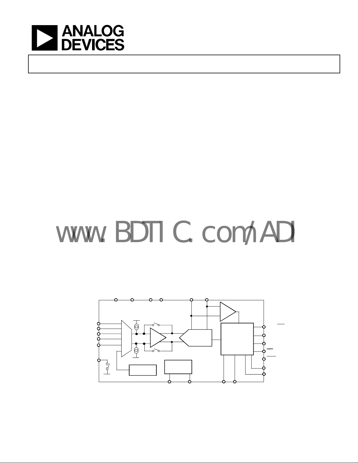
FUNCTIONAL BLOCK DIAGRAM
DD
AGNDAV
DD
DGNDDV
Sigma-Delta ADC with PGA
AD7192
PLC/DCS Analog Input Modules
Data Acquisition
Medical and Scientific instrumentation
GENERAL DESCRIPTION
The AD7192 is a low noise, complete analog front end for high
precision measurement applications. It contains a low noise, 24bit ∑-∆ ADC. The on-chip low noise gain stage means that
signals of small amplitude can be interfaced directly to the
ADC.
The device can be configured to have two differential inputs or
four pseudo-differential inputs. The device can be operated
with either the internal clock or an external clock. The output
data rate from the part can be varied from 4.7 Hz to 4.8 kHz.
The device can be operated with a sinc
At the lower output data rates, the sinc
settling time. The benefit of the sinc
the superior 50 Hz/60 Hz rejection. At the higher output data
rates, the sinc
4
filter gives best noise performance. For
applications that require all conversions to be settled, the
AD7192 includes a zero-latency feature.
The part operates with a power supply from 3 V to 5.25 V. It
consumes a current of 3.5 mA. It is housed in a 24-lead TSSOP
package.
REFIN1(+) REFIN1(-)
3
or a sinc4 digital filter.
3
is useful to optimize the
4
at low output data rates is
REFERENCE
SERIAL
INTERFACE
AND CONTROL
LOGIC
AD7192
PGA
MCLK1
CLOCK
CIRCUITRY
Figure 1.
SIGMA DELTA
ADC
MCLK2
P0/REFIN2(-)P1/REFIN2(+
One Technology Way, P.O. Box 9106, Norwood, MA 02062-9106, U.S.A.
Tel: 781.329.4700 www.analog.com
Fax: 781.461.3113 © 2008 Analog Devices, Inc. All rights reserved.
AV
MUX
DD
AGND
SENSOR
TEMP
AIN1
AIN2
AIN3
AIN4
AINCOM
BPDSW
AGND
Rev.PrE 8/08
Information furnished by Analog Devices is believed to be accurate and reliable.
However, no responsibility is assumed by Analog Devices for its use, nor for any
infringements of patents or other rights of third parties that may result from its use.
Specifications subject to change without notice. No license is granted by implication
or otherwise under any patent or patent rights of Analog Devices. Trademarks and
registered trademarks are the property of their respective owners.
DETECT
DOUT/RDY
DIN
SCLK
CS
SYNC
P3
P2
AD7192 Preliminary Technical Data
www.BDTIC.com/ADI
SPECIFICATIONS
AVDD = 3 V to 5.25 V; DVDD = 2.7 V to 5.25 V; GND = 0 V; REFIN1(+) = AVDD ; REFIN1(-) = GND; MCLK = 4.9152 MHz; Sinc4 filter
selected; all specifications T
Table 1.
Parameter1 AD7192B Unit Test Conditions/Comments
Output Data Rate 4.7 to 4800 Hz nom Chop Disabled
1.17 to 1200 Hz nom Chop Enabled
No Missing Codes2 24 Bits min FS > 1
Resolution
RMS Noise and Update Rates
Integral Nonlinearity ±15 ppm of FSR max
Offset Error3 ±100/Gain µV typ Chop Disabled
±0.5 µV typ Chop Enabled
Offset Error Drift vs. Temperature4 ±150/Gain nV/°C typ Gain = 1 to 16. Chop Disabled
±10 nV/°C typ Gain = 32 to 128. Chop Disabled
±5 nV/°C typ Chop Enabled
Offset Error Drift vs. Time 25 nV/1000 Hours typ
Full-Scale Error
Gain Drift vs. Temperature4
Gain Drift vs. Time 10 ppm/1000 Hours typ
Power Supply Rejection 100 dB min VIN = 1 V/Gain. 120 dB typical.
ANALOG INPUTS
Differential Input Voltage Ranges ± V
± (AVDD – 1V)/gain V min/max gain > 1
Absolute AIN Voltage Limits2
Unbuffered Mode
AVDD + 50 mV V max
Buffered Mode GND + 200 mV V min
Analog Input Current
Buffered Mode
Input Current2
±3 nA typ Gain > 1
Input Current Drift ±2 pA/°C typ
Unbuffered Mode
Input Current ±5 µA/V typ Gain = 1. Input current varies with input voltage
±1 µA/V typ Gain > 1.
Input Current Drift ±50 pA/V/°C typ
Normal Mode Rejection2
@ 50 Hz, 60 Hz 98 dB min 10 Hz Output Date Rate, 50 ± 1 Hz, 60 ± 1 Hz
TBD dB min 50 Hz Output Date Rate, REJ606 = 1, 50 ± 1 Hz, 60 ± 1
@ 50 Hz TBD dB min 50 Hz Output Date Rate, 50 ± 1 Hz
@ 60 Hz TBD dB min 60 Hz Output Date Rate, 60 ± 1 Hz
Common-Mode Rejection
@ DC 100 dB min AIN = 1 V/gain
@ 50 Hz, 60 Hz2
@ 50 Hz, 60 Hz2
REFERENCE INPUT
3, 5
MIN
to T
, unless otherwise noted.
MAX
See
RMS Noise and
Resolution
Specifications
See
RMS Noise and
Resolution
Specifications
±10 µV typ
±1 ppm/°C typ
/gain V nom
REF
GND − 50 mV
AV
− 200 mV
DD
±1 nA max Gain = 1
100 dB min 10 Hz Output Date Rate, 50 ± 1 Hz, 60 ± 1 Hz
100 dB min 50 ± 1 Hz (50 Hz Output Date Rate), 60 ± 1 Hz (60 Hz
V
= REFIN(+) − REFIN(−) , gain = 1 to 128
REF
V min
V max
Hz
Output Date Rate)
Rev.PrE 8/08 | Page 2
Preliminary Technical Data AD7192
www.BDTIC.com/ADI
Parameter1 AD7192B Unit Test Conditions/Comments
REFIN Voltage AVDD V nom
Reference Voltage Range2
1 V min
AVDD V max The differential input must be limited to ± (AVDD –
Absolute REFIN Voltage Limits2
GND – 50 mV V min
AVDD + 50 mV V max
Average Reference Input Current 6 µA/V typ
Average Reference Input Current
±0.03 nA/V/°C typ
Drift
Normal Mode Rejection2
Same as for analog
inputs
Common-Mode Rejection 100
dB typ
Reference Detect Levels 0.3 V min
0.5 V max
TEMPERATURE SENSOR
Accuracy +2 °C typ Applies after user-calibration at one temperature
Sensitivity 2800 codes/°C typ
LOW SIDE POWER SWITCH
RON 7
9
Allowable Current2
30 mA max Continuous Current
Ω max
Ω max
BURNOUT CURRENTS
AIN Current 500 nA nom
DIGITAL OUTPUTS (P0 – P3)
VOH, Output High Voltage2
VOL, Output Low Voltage2
VOH, Output High Voltage2
VOL, Output Low Voltage2
− 0.6
AV
DD
0.4 V max
4 V min
0.4 V max
V min
Floating-State Leakage Current ±10 µA max
Floating-State Output Capacitance 10 pF typ
INTERNAL/EXTERNAL CLOCK
Internal Clock
Frequency 4.92 + 4% MHz min/max
Duty Cycle 50:50 % typ
External Clock/Crystal
Frequency 4.9152 MHz nom
2.4576/5.12 MHz min/max
V
, Input Low Voltage 0.8 V max DVDD = 5 V
INL
0.4 V max DVDD = 3 V
V
, Input High Voltage 2.5 V min DVDD = 3 V
INH
3.5 V min DVDD = 5 V
Input Current ±10 µA max MCLKIN = DVDD or GND
LOGIC INPUTS
VT(+) 1.4/2 V min/V max DVDD = 5 V
VT(−)
VT(+) − VT(−)
0.8/1.7 V min/V max DV
0.1/0.17 V min/V max DV
VT(+) 0.9/2 V min/V max DVDD = 3 V
VT(−)
VT(+)− VT(−)
0.4/1.35 V min/V max DV
0.06/0.13 V min/V max DV
Input Currents ±10 µA max VIN = DVDD or GND
LOGIC OUTPUT (DOUT/
VOH, Output High Voltage2
VOL, Output Low Voltage2
RDY
)
DV
− 0.6
DD
V min DV
0.4 V max DV
REFIN = REFIN(+) − REFIN(−)
1V)/gain when gain > 1
AVDD = 5 V
AVDD = 3 V
AV
AV
AV
AV
= 3V, I
DD
= 3V, I
DD
= 5V, I
DD
= 5V, I
DD
= 5 V
DD
= 5 V
DD
= 3 V
DD
= 3 V
DD
= 3 V, I
DD
= 3 V, I
DD
= 100 µA
SOURCE
= 100 µA
SINK
= 200 µA
SOURCE
= 800 µA
SINK
SOURCE
= 100 µA
SINK
= 100 µA
Rev.PrE 8/08 | Page 3

AD7192 Preliminary Technical Data
www.BDTIC.com/ADI
Parameter1 AD7192B Unit Test Conditions/Comments
VOH, Output High Voltage2
VOL, Output Low Voltage2
4 V min DV
0.4 V max DV
= 5 V, I
DD
= 5 V, I
DD
Floating-State Leakage Current ±10 µA max
Floating-State Output Capacitance 10 pF typ
Data Output Coding Offset binary
SYSTEM CALIBRATION2
Full-Scale Calibration Limit 1.05 × FS V max
Zero-Scale Calibration Limit
−1.05 × FS
V min
Input Span 0.8 × FS V min
2.1 × FS V max
POWER REQUIREMENTS7
Power Supply Voltage
AVDD − AGND
DVDD − DGND
3/5.25 V min/max
2.7/5.25 V min/max
Power Supply Currents
AIDD Current TBD mA max Gain = 1, Buffer off
TBD mA max Gain = 8, Buffer off
TBD mA max Gain = 8, Buffer on
TBD mA max Gain = 16 – 128, Buffer off
TBD mA max Gain = 16 – 128, Buffer on
DIDD Current TBD mA max DVDD = 3 V
1 mA max DVDD = 5 V
IDD (Power-Down Mode) 1 µA max
1
Temperature range: −40°C to +105°C.
2
Specification is not production tested but is supported by characterization data at initial product release.
3
Following a calibration, this error will be in the order of the noise for the programmed gain and output data rate selected.
4
Recalibration at any temperature will remove these errors.
5
Full-scale error applies to both positive and negative full-scale and applies at the factory calibration conditions (AVDD = 5 V, gain = 1, TA = 25°C).
6
REJ60 is a bit in the Mode Register. When the output data rate is set to 50 Hz, setting REJ60 to ‘1’ places a notch at 60 Hz, allowing simultaneous 50 Hz/60 Hz rejection.
7
Digital inputs equal to DV
or GND.
DD
SOURCE
= 1.6 mA
SINK
= 200 µA
Rev.PrE 8/08 | Page 4
Preliminary Technical Data AD7192
www.BDTIC.com/ADI
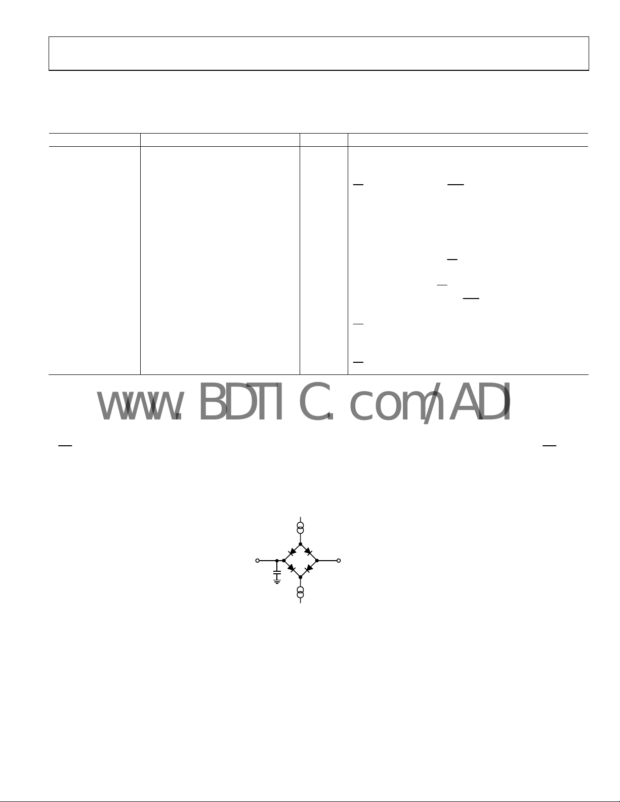
TIMING CHARACTERISTICS
AVDD = 3 V to 5.25 V; DVDD = 2.7 V to 5.25 V; GND = 0 V, Input Logic 0 = 0 V, Input Logic 1 = DVDD, unless otherwise noted.
Table 2.
Parameter
t
3
t4 100 ns min SCLK low pulse width
Read Operation
t1 0 ns min
60 ns max DVDD = 4.75 V to 5.25 V
80 ns max DVDD = 2.7 V to 3.6 V
t
60 ns max DVDD = 4.75 V to 5.25 V
80 ns max DVDD = 2.7 V to 3.6 V
t
80 ns max
t6 0 ns min
t7 10 ns min
Write Operation
t8 0 ns min
t9 30 ns min Data valid to SCLK edge setup time
t10 25 ns min Data valid to SCLK edge hold time
t11 0 ns min
1
Sample tested during initial release to ensure compliance. All input signals are specified with tR = tF = 5 ns (10% to 90% of DVDD) and timed from a voltage level of 1.6 V.
2
See Figure 3 and Figure 4.
3
These numbers are measured with the load circuit shown in Figure 2 and defined as the time required for the output to cross the VOL or VOH limits.
4
SCLK active edge is falling edge of SCLK.
5
These numbers are derived from the measured time taken by the data output to change 0.5 V when loaded with the circuit shown in Figure 2. The measured number
is then extrapolated back to remove the effects of charging or discharging the 50 pF capacitor. This means that the times quoted in the timing characteristics are the
true bus relinquish times of the part and, as such, are independent of external bus loading capacitances.
6
RDY
although care should be taken to ensure that subsequent reads do not occur close to the next output update. In continuous read mode, the digital word can be read
only once.
1, 2
Limit at T
MIN
, T
(B Version) Unit Conditions/Comments
MAX
100 ns min SCLK high pulse width
falling edge to DOUT/RDY active time
CS
3
0 ns min SCLK active edge to data valid delay4
2
5, 6
10 ns min
5
Bus relinquish time after CS
SCLK inactive edge to CS
SCLK inactive edge to DOUT/RDY
falling edge to SCLK active edge setup time4
CS
rising edge to SCLK edge hold time
CS
returns high after a read of the ADC. In single conversion mode and continuous conversion mode, the same data can be read again, if required, while
inactive edge
inactive edge
high
RDY
is high,
I
(1.6mA WITH DVDD = 5V,
SINK
100µA WITH DV
TO
OUTPUT
PIN
50pF
I
SOURCE
100µA WITH DV
Figure 2. Load Circuit for Timing Characterization
= 3V)
DD
1.6V
(200µA WITH DVDD = 5V,
= 3V)
DD
04854-002
Rev.PrE 8/08 | Page 5
AD7192 Preliminary Technical Data
S
www.BDTIC.com/ADI
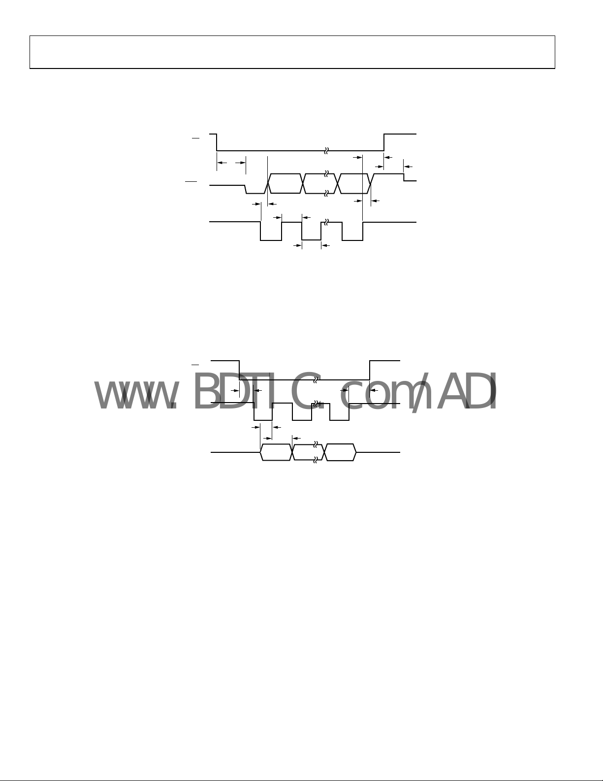
TIMING DIAGRAMS
CS (I)
t
t
1
DOUT/RDY (O)
SCLK (I)
t
2
I = INPUT, O = OUTPUT
MSB LSB
t
3
t
4
Figure 3. Read Cycle Timing Diagram
6
t
5
t
7
04854-003
CS (I)
t
11
04854-004
CLK (I)
DIN (I)
I = INPUT, O = OUTPUT
t
8
t
9
t
10
MSB LSB
Figure 4. Write Cycle Timing Diagram
Rev.PrE 8/08 | Page 6
Preliminary Technical Data AD7192
www.BDTIC.com/ADI
ABSOLUTE MAXIMUM RATINGS
TA = 25°C, unless otherwise noted.
Table 3.
Parameter Rating
AVDD to GND
DVDD to GND
Analog Input Voltage to GND
Reference Input Voltage to GND
Digital Input Voltage to GND
Digital Output Voltage to GND
AIN/Digital Input Current 10 mA
Operating Temperature Range
Storage Temperature Range
Maximum Junction Temperature 150°C
TSSOP
θJA Thermal Impedance 97.9°C/W
θJC Thermal Impedance 14°C/W
Lead Temperature, Soldering
Vapor Phase (60 sec) 215°C
Infrared (15 sec) 220°C
−0.3 V to +6.5 V
−0.3 V to +6.5 V
−0.3 V to AVDD + 0.3 V
−0.3 V to AVDD + 0.3 V
−0.3 V to DVDD + 0.3 V
−0.3 V to DVDD + 0.3 V
−40°C to +105°C
−65°C to +150°C
Stresses above those listed under Absolute Maximum Ratings
may cause permanent damage to the device. This is a stress
rating only; functional operation of the device at these or any
other conditions above those listed in the operational sections
of this specification is not implied. Exposure to absolute
maximum rating conditions for extended periods may affect
device reliability.
ESD CAUTION
ESD (electrostatic discharge) sensitive device. Electrostatic charges as high as 4000 V readily accumulate on the
human body and test equipment and can discharge without detection. Although this product features
proprietary ESD protection circuitry, permanent damage may occur on devices subjected to high energy
electrostatic discharges. Therefore, proper ESD precautions are recommended to avoid performance
degradation or loss of functionality.
Rev.PrE 8/08 | Page 7

AD7192 Preliminary Technical Data
www.BDTIC.com/ADI
PIN CONFIGURATION AND FUNCTION DESCRIPTIONS
MCLK1
MCLK2
P1/REFIN2(+)
P0/REFIN2(-)
AINCOM
1
2
SCLK
3
CS
4
AD7192
P3
P2
NC
AIN1
AIN2
TOP VIEW
5
(Not To
6
Scale)
7
8
9
10
11
12
Figure 5. Pin Configuration
2423DIN
2221SYNC
20
19
18
17
1615REFIN1(-)
14
13
DOUT/RDY
DV
DD
AV
DD
DGND
AGND
BPDSW
REFIN1(+)
AIN4
AIN3
Table 4. Pin Function Descriptions
Pin No. Mnemonic Description
1 MCLK1
When the master clock for the device is provided externally by a crystal, the crystal is connected between
MCLK1 and MCLK2.
2 MCLK2
Master Clock signal for the device. The AD7192 has an internal 4.92 MHz clock. This internal clock can be
made available on the MCLK2 pin.
The clock for the AD7192 can be provided externally also in the form of a crystal or external clock. A crystal
can be tied across the MCLK1 and MCLK2 pins. Alternatively, the MCLK2 pin can be driven with a CMOScompatible clock and MCLK1 left unconnected.
3 SCLK
Serial Clock Input. This serial clock input is for data transfers to and from the ADC. The SCLK has a Schmitttriggered input, making the interface suitable for opto-isolated applications. The serial clock can be
continuous with all data transmitted in a continuous train of pulses. Alternatively, it can be a
noncontinuous clock with the information being transmitted to or from the ADC in smaller batches of data.
4
Chip Select Input. This is an active low logic input used to select the ADC. CS can be used to select the ADC
CS
in systems with more than one device on the serial bus or as a frame synchronization signal in
communicating with the device. CS can be hardwired low, allowing the ADC to operate in 3-wire mode
with SCLK, DIN, and DOUT used to interface with the device.
5 P3 Digital Output Pin. This pin can function as a general purpose output bit referenced between AVDD and AGND.
6 P2 Digital Output Pin. This pin can function as a general purpose output bit referenced between AVDD and AGND.
7 P1/REFIN2(+) Digital Output Pin/Positive Reference Input.
This pin functions as a general purpose output bit referenced between AV
and AGND.
DD
When REFSEL = 1, this pin functions as REFIN2(+). An external reference can be applied between REFIN2(+)
and REFIN2(−). REFIN2(+) can lie anywhere between AV
(REFIN2(+) − REFIN2(−)), is AV
, but the part functions with a reference from 1 V to AVDD.
DD
and GND + 1 V. The nominal reference voltage,
DD
8 P0/REFIN2(-) Digital Output Pin/Negative Reference Input.
This pin functions as a general purpose output bit referenced between AV
and AGND.
DD
When REFSEL = 1, this pin functions as REFIN2(-). This reference input can lie anywhere between GND and
AV
− 1 V.
DD
9 NC No Connect. This pin should be tied to AGND.
10 AINCOM
11 AIN1
Analog inputs AIN1 to AIN4 are referenced to this input when configured for pseudo-differential operation.
Analog Input. It can be configured as the positive input of a fully differential input pair when used with
AIN2 or as a pseudo-differential input when used with AINCOM.
12 AIN2
Analog Input. It can be configured as the negative input of a fully differential input pair when used with
AIN1 or as a pseudo-differential input when used with AINCOM.
13 AIN3
Analog Input. It can be configured as the positive input of a fully differential input pair when used with
Rev.PrE 8/08 | Page 8

Preliminary Technical Data AD7192
www.BDTIC.com/ADI
Pin No. Mnemonic Description
AIN4 or as a pseudo-differential input when used with AINCOM.
14 AIN4
15 REFIN1(+)
16 REFIN1(−) Negative Reference Input. This reference input can lie anywhere between GND and AVDD − 1 V.
17 BPDSW
18 AGND Analog Ground Reference Point.
19 DGND Digital Ground Reference Point.
20 AVDD
21 DVDD
22
23
24 DIN
SYNC
DOUT/RDY
Serial Data Output/Data Ready Output. DOUT/RDYserves a dual purpose. It functions as a serial data
Analog Input. It can be configured as the negative input of a fully differential input pair when used with
AIN3 or as a pseudo-differential input when used with AINCOM.
Positive Reference Input. An external reference can be applied between REFIN1(+) and REFIN1(−).
REFIN1(+) can lie anywhere between AV
REFIN1(−)), is AV
Low Side Power Switch to AGND.
Analog Supply Voltage, 3 V to 5.25 V. AV
with AV
Digital Supply Voltage, 2.7 V to 5.25 V. DV
with DV
Logic Input that allows for synchronization of the digital filters and analog modulators when using a
number of AD7192 devices. While SYNC
calibration control logic are reset and the analog modulator is also held in its reset state. SYNC
affect the digital interface but does reset RDY to a high state if it is low. SYNC has a pull- up resistor
internally to DV
output pin to access the output shift register of the ADC. The output shift register can contain data from
any of the on-chip data or control registers. In addition, DOUT/RDYoperates as a data ready pin, going low
to indicate the completion of a conversion. If the data is not read after the conversion, the pin will go high
before the next update occurs.
The DOUT/RDY
available. With an external serial clock, the data can be read using the DOUT/RDY
data/control word information is placed on the DOUT/RDY pin on the SCLK falling edge and is valid on the
SCLK rising edge.
Serial Data Input to the Input Shift Register on the ADC. Data in this shift register is transferred to the
control registers within the ADC, the register selection bits of the communications register identifying the
appropriate register.
at 5 V or vice versa.
DD
at 5 V or vice versa.
DD
, but the part functions with a reference from 1 V to AVDD.
DD
.
DD
falling edge can be used as an interrupt to a processor, indicating that valid data is
and GND + 1 V. The nominal reference voltage, (REFIN1(+) −
DD
is independent of DVDD. Therefore DVDD can be operated at 3 V
DD
is independent of AVDD. Therefore AVDD can be operated at 3 V
DD
is low, the nodes of the digital filter, the filter control logic and the
does not
pin. With CS low, the
Rev.PrE 8/08 | Page 9
AD7192 Preliminary Technical Data
www.BDTIC.com/ADI
RMS NOISE AND RESOLUTION SPECIFICATIONS
The AD7192 can be operated with chop enabled or chop
disabled. With chop enabled, the settling time is two times the
conversion time. The offset is continuously removed by the
ADC leading to low offset and low offset drift. With chop
disabled, higher output data rates can be achieved from the
ADC. The settling time is three times (sinc
4
) the selected output data rate. With chop disabled, the
(sinc
offset is not removed by the ADC. The offset and offset drift is
comparable between chop enabled and chop disabled for gains
of 32 or higher. For lower gains, however, periodic offset
calibrations may be required to remove offset due to drift.
3
) or four times
SINC4 FILTER
The sinc4 filter optimizes the 50 Hz/60 Hz rejection. At the
higher output data rates, it also gives better rms noise
performance compared with the sinc
Table 5. RMS Noise (nV) vs. Gain and Output Data Rate(continuous conversion mode) Using a 5 V Reference - Chop Disabled
Filter Word
(Decimal)
1023 4.7
640 7.5
480 10
96 50
80 60
32 150
16 300
5 960
2 2400
1 4800
Table 6. Typical Resolution (Bits) vs. Gain and Output Data Rate(continuous conversion mode) Using a 5 V Reference - Chop
Disabled
Filter Word
(Decimal)
1023 4.7
640 7.5
480 10
96 50
80 60
32 150
16 300
32 960
2 2400
1 4800
Output Data
Rate(Hz)
Output Data
Rate(Hz)
3
filter.
Settling Time
(ms)
851 350 50 30 18 13 11
533 410 60 36 22 16.5 14
400 460 70 40 24 19 17
80 1100 157 90 53 41 37
66.7 1400 183 100 64 46 40
26.7 2360 325 185 110 75 65
13.3 3000 430 240 145 105 93
4.17 4800 700 390 250 185 160
1.67 7400 1100 640 400 300 260
0.83 16200 2200 1200 680 465 387
Settling Time
(ms)
851
533
400
80
66.7
26.7
13.3
4.17
1.67
0.83
Gain of 1 Gain of 8 Gain of 16 Gain of 32 Gain of 64 Gain of 128
Gain of 1 Gain of 8 Gain of 16 Gain of 32 Gain of 64 Gain of 128
24 (22) 24 (22) 24 (21.5) 24 (21.5) 23.5 (21) 22.5 (20)
24 (22) 24 (21.5) 24 (21.5) 23.5 (21) 23 (20.5) 22 (19.5)
24 (21.5) 24 (21.5) 23.5 (21) 23.5 (21) 22.5 (20) 22 (19.5)
23 (20.5) 22.5 (20) 22.5 (20) 22.5 (20) 21.5 (19) 21 (18.5)
22.5 (20) 22.5 (20) 22.5 (20) 22 (19.5) 21.5 (19) 20.5 (18)
22 (19.5) 21.5 (19) 21.5 (19) 21 (18.5) 21 (18.5) 20 (17.5)
21.5 (19) 21 (18.5) 21 (18.5) 21 (18.5) 20.5 (18) 19.5 (17)
21 (18.5) 20.5 (18) 20.5 (18) 20 (17.5) 19.5 (17) 18.5 (16)
20 (17.5) 20 (17.5) 19.5 (17) 19.5 (17) 19 (16.5) 18 (15.5)
19 (16.5) 19 (16.5) 19 (16.5) 18.5 (16) 18 (15.5) 17.5 (15)
CHOP DISABLED
Table 5 shows the rms noise of the AD7192 for some of the
output data rates and gain settings with chop disabled. The
numbers given are for the bipolar input range with the
external 5 V reference. These numbers are typical and are
generated with a differential input voltage of 0 V. Table 6
shows the effective resolution while the output peak-to-peak
(p-p) resolution is listed in brackets. It is important to note
that the effective resolution is calculated using the rms noise,
while the p-p resolution is calculated based on peak-to-peak
noise. The p-p resolution represents the resolution for which
there will be no code flicker. These numbers are typical and
are rounded to the nearest half-LSB.
Rev.PrE 8/08 | Page 10

Preliminary Technical Data AD7192
www.BDTIC.com/ADI
CHOP ENABLED
Table 7 shows the AD7192’s rms noise for some of the update
rates and gain settings. The numbers given are for the bipolar
input range with an external 5 V reference. These numbers are
typical and are generated with a differential input voltage of 0 V.
Table 8 shows the effective resolution, while the output peak-topeak (p-p) resolution is listed in brackets. It is important to note
Table 7. RMS Noise (nV) vs. Gain and Output Data Rate(continuous conversion mode) Using a 5 V Reference - Chop Enabled
Filter Word
(Decimal)
1023 1.175
640 1.875
480 2.5
96 12.5
80 15
32 37.5
16 75
5 240
2 600
1 1200
Table 8. Typical Resolution (Bits) vs. Gain and Output Data Rate(continuous conversion mode) Using a 5 V Reference - Chop
Enabled
Filter Word
(Decimal)
1023 1.175
640 1.875
480 2.5
96 12.5
80 15
32 37.5
16 75
5 240
2 600
1 1200
Output Data
Rate(Hz)
Output Data
Rate(Hz)
Settling
Time (ms)
1702
1067
800
160
133
53.3
26.7
8.33
3.33
1.67
Settling
Time (ms)
1702
1067
800
160
133
53.3
26.7
8.33
3.33
1.67
Gain of 1 Gain of 8 Gain of 16 Gain of 32 Gain of 64 Gain of 128
248 36 22 13 10 8
290 43 26 16 12 10
326 50 29 17 14 12
778 111 64 38 29 27
990 130 71 46 33 29
1669 230 131 78 53 46
2122 304 170 103 75 66
3395 495 276 177 131 114
5233 778 453 283 213 184
11456 1556 849 481 329 274
Gain of 1 Gain of 8 Gain of 16 Gain of 32 Gain of 64 Gain of 128
24 (22.5) 24 (22.5) 24 (22) 24 (22) 24 (21.5) 23 (20.5)
24 (22.5) 24 (22) 24 (22) 24 (21.5) 23.5 (21) 22.5 (20)
24 (22) 24 (22) 24 (21.5) 24 (21.5) 23 (20.5) 22.5 (20)
23.5 (21) 23 (20.5) 23 (20.5) 23 (20.5) 22 (19.5) 21.5 (19)
23 (20.5) 23 (20.5) 23 (20.5) 22.5 (20) 22 (19.5) 21 (18.5)
22.5 (20) 22 (19.5) 22 (19.5) 21.5 (19) 21.5 (19) 20.5 (18)
22 (19.5) 21.5 (19) 21.5 (19) 21.5 (19) 21 (18.5) 20 (17.5)
21.5 (19) 21 (18.5) 21 (18.5) 20.5 (18) 20 (17.5) 19 (16.5)
20.5 (18) 20.5 (18) 20 (17.5) 20 (17.5) 19.5 (17) 18.5 (16)
19.5 (17) 19.5 (17) 19.5 (17) 19 (16.5) 18.5 (16) 18 (15.5)
that the effective resolution is calculated using the rms noise,
while the p-p resolution is calculated based on peak-to-peak
noise. The p-p resolution represents the resolution for which
there will be no code flicker. These numbers are typical and are
rounded to the nearest half-LSB.
Rev.PrE 8/08 | Page 11

AD7192 Preliminary Technical Data
www.BDTIC.com/ADI
SINC3 FILTER
For a given update rate, the sinc3 filter has lower settling time
than the sinc
comparable between the sinc
user can optimize the settling time without compromising the
rms noise. At high update rates, the sinc
optimum performance of the AD7192.
3
filter. At low update rates, the rms noise is
3
filter and the sinc4 filter. So, the
4
filter is needed for
CHOP DISABLED
Table 9 shows the rms noise of the AD7192 for some of the
update rates and gain settings with chop disabled. The
Table 9. RMS Noise (nV) vs. Gain and Output Data Rate(continuous conversion mode) Using a 5 V Reference - Chop Disabled
Filter Word
(Decimal)
1023 4.7
640 7.5
480 10
96 50
80 60
32 150
16 300
5 960
2 2400
1 4800
Table 10. Typical Resolution (Bits) vs. Gain and Output Data Rate(continuous conversion mode) Using a 5 V Reference - Chop
Disabled
Filter Word
(Decimal)
1023 4.7
640 7.5
480 10
96 50
80 60
32 150
16 300
5 960
2 2400
1 4800
Output Data
Rate(Hz)
Output Data
Rate(Hz)
Settling
Time (ms)
638 400
400 426
300 520
60 1300
50 1450 200 110 68 49 44
20 2450 348 198 116 81 68
10 3200 454 265 153 114
3.13 5600 800 455 275 199 175
1.25 55800 7100 3600 1750 930
0.625 443000 55400 27500 14000 7000 3500
Settling
Time (ms)
638 24 (22) 24 (21.5) 24 (21.5) 23.5 (21) 23 (20.5) 22.5 (20)
400 24 (22) 24 (21.5) 24 (21.5) 23.5 (21) 23 (20.5) 22 (19.5)
300 24 (21.5) 23.5 (21) 23.5 (21) 23 (20.5) 22.5 (20) 22 (19.5)
60 22.5 (20) 22.5 (20) 22.5 (20) 22 (19.5) 21.5 (19) 20.5 (18)
50 22.5 (20) 22.5 (20) 22 (19.5) 22 (19.5) 21.5 (19) 20.5 (18)
20 21.5 (19) 21.5 (19) 21.5 (19) 21 (18.5) 20.5 (18) 20 (17.5)
10 21.5 (19) 21.5 (19) 21 (18.5) 20.5 (18) 20 (17.5) 19.5 (17)
3.13 20.5 (18) 20.5 (18) 20 (17.5) 20 (17.5) 19.5 (17) 18.5 (16)
1.25 17 (14.5) 17 (14.5) 17 (14.5) 17 (14.5) 17 (14.5) 17 (14.5)
0.625 14 (11.5) 14 (11.5) 14 (11.5) 14 (11.5) 14 (11.5) 14 (11.5)
Gain of 1 Gain of 8 Gain of 16 Gain of 32 Gain of 64 Gain of 128
56
67
76
176
Gain of 1 Gain of 8 Gain of 16 Gain of 32 Gain of 64 Gain of 128
numbers given are for the bipolar input range with the
external 5 V reference. These numbers are typical and are
generated with a differential input voltage of 0 V. Table 10
shows the effective resolution while the output peak-to-peak
(p-p) resolution is listed in brackets. It is important to note
that the effective resolution is calculated using the rms noise,
while the p-p resolution is calculated based on peak-to-peak
noise. The p-p resolution represents the resolution for which
there will be no code flicker. These numbers are typical and
are rounded to the nearest half-LSB.
30 20 15 12
36 25 18
40 27 20 18
100 61 47
15
40
98
530
Rev.PrE 8/08 | Page 12
Preliminary Technical Data AD7192
www.BDTIC.com/ADI
CHOP ENABLED
Table 11 shows the AD7192’s rms noise for some of the update
rates and gain settings. The numbers given are for the bipolar
input range with an external 5 V reference. These numbers are
typical and are generated with a differential input voltage of 0 V.
Ta bl e 12 shows the effective resolution, while the output peakto-peak (p-p) resolution is listed in brackets. It is important to
Table 11. RMS Noise (nV) vs. Gain and Output Data Rate(continuous conversion mode) Using a 5 V Reference - Chop Enabled
Filter Word
(Decimal)
1023 1.56
640 2.5
480 3.33
96 16.6
80 20
32 50
16 100
5 320
2 800
1 1600
Table 12. Typical Resolution (Bits) vs. Gain and Output Data Rate(continuous conversion mode) Using a 5 V Reference - Chop
Enabled
Filter Word
(Decimal)
1023 1.56
640 2.5
480 3.33
96 16.6
80 20
32 320
16 100
5 320
2 800
1 1600
Output Data
Rate(Hz)
Output Data
Rate(Hz)
Settling Time
(ms)
1282
800
600
120
100
40
20
6.25
2.5
1.25
Settling Time
(ms)
1282
800
600
120
100 23 (20.5) 23 (20.5) 22.5 (20) 22.5 (20) 22 (19.5) 21 (18.5)
40
20
6.25
2.5
1.25
Gain of 1 Gain of 8 Gain of 16 Gain of 32 Gain of 64 Gain of 128
283 40 22 15 11 8.5
302 48 26 18 13 11
368 54 29 19 15 13
920 125 71 44 34 29
1026 142 78 48 35 32
1733 246 140 82 58 48
2265 321 188 109 81 70
3960 566 322 195 141 124
39460 5100 2550 1240 658 375
313300 39200 19500 9900 4950 2475
Gain of 1 Gain of 8 Gain of 16 Gain of 32 Gain of 64 Gain of 128
24 (22.5) 24 (22) 24 (22) 24 (21.5) 23.5 (21) 23 (20.5)
24 (22.5) 24 (22) 24 (22) 24 (21.5) 23.5 (21) 22.5 (20)
24 (22) 24 (21.5) 24 (21.5) 23.5 (21) 23 (20.5) 22.5 (20)
23 (20.5) 23 (20.5) 23 (20.5) 22.5 (20) 22 (19.5) 21 (18.5)
22 (19.5) 22 (19.5) 22 (19.5) 21.5 (19) 21 (18.5) 20.5 (18)
22 (19.5) 22 (19.5) 21.5 (19) 21 (18.5) 20.5 (18) 20 (17.5)
21 (18.5) 21 (18.5) 20.5 (18) 20.5 (18) 20 (17.5) 19 (16.5)
17.5 (15) 17.5 (15) 17.5 (15) 17.5 (15) 17.5 (15) 17.5 (15)
14.5 (12) 14.5 (12) 14.5 (12) 14.5 (12) 14.5 (12) 14.5 (12)
note that the effective resolution is calculated using the rms
noise, while the p-p resolution is calculated based on peak-topeak noise. The p-p resolution represents the resolution for
which there will be no code flicker. These numbers are typical
and are rounded to the nearest half-LSB.
Rev.PrE 8/08 | Page 13

AD7192 Preliminary Technical Data
www.BDTIC.com/ADI
TYPICAL PERFORMANCE CHARACTERISTICS
Figure 6.
Figure 7.
Figure 9.
Figure 10.
Figure 8.
Rev.PrE 8/08 | Page 14
Figure 11.

Preliminary Technical Data AD7192
www.BDTIC.com/ADI
ON-CHIP REGISTERS
The ADC is controlled and configured via a number of on-chip
registers, which are described on the following pages. In the
following descriptions, set implies a Logic 1 state and cleared
implies a Logic 0 state, unless otherwise noted.
COMMUNICATIONS REGISTER
(RS2, RS1, RS0 = 0, 0, 0)
The communications register is an 8-bit write-only register. All
communications to the part must start with a write operation to
the communications register. The data written to the communications register determines whether the next operation is a read
or write operation, and to which register this operation takes
place. For read or write operations, once the subsequent read or
CR7 CR6 CR5 CR4 CR3 CR2 CR1 CR0
WEN(0) R/W(0)
Table 13. Communications Register Bit Designations
Bit Location Bit Name Description
CR7
CR6
CR5 to CR3 RS2 to RS0
CR2 CREAD
CR1 to CR0 0 These bits must be programmed to Logic 0 for correct operation.
Table 14. Register Selection
RS2 RS1 RS0 Register Register Size
0 0 0 Communications Register During a Write Operation 8-bit
0 0 0 Status Register During a Read Operation 8-bit
0 0 1 Mode Register 24-bit
0 1 0 Configuration Register 24-bit
0 1 1 Data Register / Data Register + Status Information 24-bit / 32-bit
1 0 0 ID Register 8-bit
1 0 1 GPOCON Register 8-bit
1 1 0 Offset Register 24-bit
1 1 1 Full-Scale Register 24-bit
Write Enable Bit. A 0 must be written to this bit so that the write to the communications register actually
WEN
A 0 in this bit location indicates that the next operation will be a write to a specified register. A 1 in this
R/W
RS2(0) RS1(0) RS0(0) CREAD(0) 0(0) 0(0)
occurs. If a 1 is the first bit written, the part will not clock on to subsequent bits in the register. It will stay at
this bit location until a 0 is written to this bit. Once a 0 is written to the WEN
loaded to the communications register.
position indicates that the next operation will be a read from the designated register.
Register Address Bits. These address bits are used to select which registers of the ADC are being selected
during this serial interface communication. See Table 14.
Continuous Read of the Data Register. When this bit is set to 1 (and the data register is selected), the serial
interface is configured so that the data register can be continuously read, that is, the contents of the data
register are automatically placed on the DOUT pin when the SCLK pulses are applied after the RDY
goes low to indicate that a conversion is complete. The communications register does not have to be
written to for subsequent data reads. To enable continuous read, the instruction 01011100 must be written
to the communications register. To disable continuous read, the instruction 01011000 must be written to
the communications register while the RDY pin is low. While continuous read is enabled, the ADC monitors
activity on the DIN line so that it can receive the instruction to disable continuous read. Additionally, a
reset will occur if 40 consecutive 1s are seen on DIN. Therefore, DIN should be held low until an instruction
is to be written to the device.
write operation to the selected register is complete, the interface
returns to where it expects a write operation to the communications register. This is the default state of the interface and, on
power-up or after a reset, the ADC is in this default state
waiting for a write operation to the communications register. In
situations where the interface sequence is lost, a write operation
of at least 40 serial clock cycles with DIN high returns the ADC
to this default state by resetting the entire part. Table 13 outlines
the bit designations for the communications register. CR0
through CR7 indicate the bit location, CR denoting the bits are
in the communications register. CR7 denotes the first bit of the
data stream. The number in brackets indicates the poweron/reset default status of that bit.
bit, the next seven bits will be
pin
Rev.PrE 8/08 | Page 15

AD7192 Preliminary Technical Data
www.BDTIC.com/ADI
STATUS REGISTER
(RS2, RS1, RS0 = 0, 0, 0; Power-On/Reset = 0x80)
The status register is an 8-bit read-only register. To access the ADC status register, the user must write to the communications register,
select the next operation to be a read, and load Bit RS2, Bit RS1, and Bit RS0 with 0. Table 15 outlines the bit designations for the status
register. SR0 through SR7 indicate the bit locations, SR denoting the bits are in the status register. SR7 denotes the first bit of the data
stream. The number in brackets indicates the power-on/reset default status of that bit.
SR7 SR6 SR5 SR4 SR3 SR2 SR1 SR0
RDY(1)
Table 15. Status Register Bit Designations
Bit Location Bit Name Description
SR7
SR6 ERR
SR5 NOREF
SR4 PARITY Parity Check of Data Register.
SR3 to SR0
MODE REGISTER
(RS2, RS1, RS0 = 0, 0, 1; Power-On/Reset = 0x080060)
ERR(0) NOREF(0) PARITY(0) CHD3(0) CHD2(0) CHD1(0) CHD0(0)
Ready Bit for ADC. Cleared when data is written to the ADC data register. The RDY bit is set automatically
RDY
after the ADC data register has been read or a period of time before the data register is updated with a
new conversion result to indicate to the user not to read the conversion data. It is also set when the part is
placed in power-down mode, idle mode or when SYNC is taken low.
pin. This pin can be used as an alternative to
bit. Set to indicate that the result written to
CHD3 to
CHD0
The end of a conversion is also indicated by the DOUT/RDY
the status register for monitoring the ADC for conversion data.
ADC Error Bit. This bit is written to at the same time as the RDY
the ADC data register has been clamped to all 0s or all 1s. Error sources include overrange, underrange, or
the absence of a reference voltage. Cleared by a write operation to start a conversion.
No External Reference Bit. Set to indicate that the selected reference (REFIN1 or REFIN2) is at a voltage that
is below a specified threshold. When set, conversion results are clamped to all ones. Cleared to indicate
that a valid reference is applied to the selected reference pins. The NOXREF bit is enabled by setting the
REF_DET bit in the configuration register to 1. The ERR bit is also set if the voltage applied to the selected
reference input is invalid.
If the ENPAR bit is set, the PARITY bit is set if there is an odd number of 1s in the data register. It is cleared if
there is an even number of 1s in the data register. The DAT_STA bit should be set when the parity check is
used. When the DAT_STA bit is set, the contents of the status register are transmitted along with the data
for each data register read.
These bits indicate which channel corresponds to the data register contents. They do not indicate which
channel is presently being converted but indicate which channel was selected when the conversion
contained in the data register was being generated.
The mode register is a 24-bit register from which data can be read or to which data can be written. This register is used to select the
operating mode, the update rate, and the clock source. Table 16 outlines the bit designations for the mode register. MR0 through MR23
indicate the bit locations, MR denoting the bits are in the mode register. MR23 denotes the first bit of the data stream. The number in
brackets indicates the power-on/reset default status of that bit. Any write to the mode register resets the modulator and filter and sets the
RDY
bit.
MR23 MR22 MR21 MR20 MR19 MR18 MR17 MR16
MD2(0) MD1(0) MD0(0) DAT_STA(0) CLK1(1) CLK0(0) 0 0
MR15 MR14 MR13 MR12 MR11 MR10 MR9 MR8
SINC3(0) 0 ENPAR(0) 0 SINGLE(0) REJ60(0) FS9(0) FS8(0)
MR7 MR6 MR5 MR4 MR3 MR2 MR1 MR0
FS7(0) FS6(1) FS5(1) FS4(0) FS3(0) FS2(0) FS1(0) FS0(0)
Table 16. Mode Register Bit Designations
Bit Location Bit Name Description
MR23 to MR21 MD2 to MD0 Mode Select Bits. These bits select the operational mode of the AD7192 (see Table 17).
MR20 DAT_STA Transmit status register contents after each data register read.
When DAT_STA is set, the contents of the status register are transmitted along with each data register
Rev.PrE 8/08 | Page 16

Preliminary Technical Data AD7192
www.BDTIC.com/ADI
Bit Location Bit Name Description
read. This function is useful when several channels are selected as the status register identifies the
channel to which the data register value corresponds.
MR19 to MR18 CLK1 to CLK0
0 0 External crystal used. The external crystal is connected from MCLK1 to MCLK2.
0 1 External clock used. The external clock is applied to the MCLK2 pin.
1 0 Internal 4.92 MHz clock. Pin MCLK2 is tri-stated.
1 1 Internal 4.92 MHz clock. The internal clock is available on MCLK2.
MR17 to MR16 0 These bits must be programmed with a Logic 0 for correct operation.
MR15 SINC3 Sinc3 Filter Select pin.
MR14 0 This bit must be programmed with a Logic 0 for correct operation.
MR13 ENPAR Enable Parity bit.
MR12 0 This bit must be programmed with a Logic 0 for correct operation.
MR11 SINGLE Single Cycle Conversion Enable Bit.
MR10 REJ60 Enables a notch at 60 Hz when the output data rate is equal to 50 Hz.
MR9 to MR0 FS9 to FS0 Filter Output Data Rate Select Bits.
These bits are used to select the clock source for the AD7192. Either the on-chip 4.92 MHz clock can
be used or an external clock can be used. The ability to use an external clock allows several AD7192
devices to be synchronized. Also, 50 Hz/60 Hz rejection is improved when an accurate external clock
drives the AD7192.
CLK1 CLK0 ADC Clock Source
When this bit is cleared, the sinc
When this bit is set, a sinc
The benefit of the sinc3 filter compared to the sinc4 filter is its lower settling time when chop is
disabled. For a given output data rate f
filter has a settling time of f
rejection.
At low update rates, both filters give similar rms noise and similar no missing codes for a given update
rate. At higher update rates (FS values less than 5), the sinc
3
sinc
filter for rms noise and no missing codes.
When ENPAR is set, parity checking on the data register is enabled. The DAT_STA bit should be set
when the parity check is used. When the DAT_STA bit is set, the contents of the status register are
transmitted along with the data for each data register read.
When this bit is set, the AD7192 allows the complete settling time to perform each conversion. So, the
device functions as a zero-latency ADC.
When REJ60 is set, a filter notch is placed at 60 Hz when the output data rate selected is 50 Hz. This
allows simultaneous 50 Hz/60 Hz rejection.
The 10 bits of data programmed into these bits determine the filter cut-off frequency, the position of
the first notch of the filter and the output data rate for the part. In association with the gain selection,
it also determines the output noise (and hence the effective resolution) of the device. When chop is
disabled and continuous conversion mode is selected, the first notch of the filter occurs at a frequency
determined by the relationship:
filter first notch frequency = (fmod/64)/FS
where FS is the decimal equivalent of the code in bits FS0 to FS9 and is in the range 1 to 1023 and
fmod is the modulator frequency which is equal to MCLK/16. With the nominal MCLK of 4.92 MHz, this
results in a first notch frequency range from 4.69 Hz to 4.8 kHz.
Changing the filter notch frequency, as well as the selected gain, impacts resolution. Tables 5 through
8 show the effect of the filter notch frequency and gain on the effective resolution of the AD7192. The
output data rate (or effective conversion time) for the device is equal to the frequency selected for the
first notch of the filter. For example, if the first notch of the filter is selected at 50 Hz then a new word
is available at a 50 Hz rate or every 20 ms. If the first notch is at 1.2 kHz, a new word is available every
0.83 ms. The settling time of the filter to a full-scale step input change is worst case (N + 1)/(output
data rate) where N = 3 when the sinc
example, with the first filter notch at 50 Hz, the settling time of the filter to a full-scale step input
change is 100 ms max when N = 4. This settling time can be reduced to N/(output data rate) by
synchronizing the step input change to a reset of the digital filter. In other words, if the step input
takes place with the SYNC
returns high. If a change of channel takes place, the settling time is N/(output data rate) regardless of
the SYNC
The –3 dB frequency is determined by the programmed first notch frequency according to the
status as the part issues an internal reset command when requested to change channels.
4
filter is used (default value).
3
filter is used.
, the sinc3 filter has a settling time of f
/4. The sinc4 filter, due to its deeper notches, gives better 50 Hz/60 Hz
ADC
input low, the settling time will be N/(output data rate) from when SYNC
ADC
4
filter gives better performance than the
3
filter is selected and N = 4 when the sinc4 filter is selected. For
/3 while the sinc4
ADC
Rev.PrE 8/08 | Page 17

AD7192 Preliminary Technical Data
www.BDTIC.com/ADI
Bit Location Bit Name Description
relationship:
filter –3 dB frequency = 0.23 x filter first notch frequency.
When chop is enabled, the output data rate equals
Output data rate = (fmod/64)/(NxFS)
where FS is the decimal equivalent of the code in bits FS0 to FS9 and is in the range 1 to 1023 and
fmod is the modulator frequency which is equal to MCLK/16. With the nominal MCLK of 4.92 MHz, this
results in an output data rate from 4.69/N Hz to 4.8/N kHz where N is the order of the sinc filter. The
first notch in the frequency response is placed at output data rate/2. The settling time is equal to 2 x
Table 17. Operating Modes
MD2 MD1 MD0 Mode
0 0 0 Continuous Conversion Mode (Default).
0 0 1 Single Conversion Mode.
0 1 0 Idle Mode.
In idle mode, the ADC filter and modulator are held in a reset state although the modulator clocks are still provided.
0 1 1 Power-Down Mode.
1 0 0 Internal Zero-Scale Calibration.
1 0 1 Internal Full-Scale Calibration.
A full-scale input voltage is automatically connected to the input for this calibration.
1 1 0 System Zero-Scale Calibration.
1 1 1 System Full-Scale Calibration.
User should connect the system full-scale input to the channel input pins as selected by the CH7–CH0 bits.
A full-scale calibration is required each time the gain of a channel is changed.
In continuous conversion mode, the ADC continuously performs conversions and places the result in the data
register. RDY goes low when a conversion is complete. The user can read these conversions by setting the CREAD
bit in the communications register to ‘1’ which enables continuous read. When continuous read is enabled, the
conversions are automatically placed on the DOUT line when SCLK pulses are applied. Alternatively, the user can
instruct the ADC to output each conversion by writing to the communications register.
After power-on, a reset or a re-configuration of the ADC, the complete settling time of the filter is required to
generate the first valid conversion. Subsequent conversions are available at the selected output data rate which is
dependent on filter choice.
When single conversion mode is selected, the ADC powers up and performs a single conversion on the selected
channel. The oscillator requires 1 ms to power up and settle. The ADC then performs the conversion which requires
the complete settling time of the filter. The conversion result is placed in the data register, RDY
ADC returns to power-down mode. The conversion remains in the data register and RDY remains active (low) until
the data is read or another conversion is performed.
In power-down mode, all the AD7192 circuitry, except the power switch, is powered down. The power switch
remains active as the user may need to power up the sensor prior to powering up the AD7192 for settling reasons.
The external crystal, if present, is left active.
An internal short is automatically connected to the input. RDY
returns low when the calibration is complete. The ADC is placed in idle mode following a calibration. The measured
offset coefficient is placed in the offset register of the selected channel.
RDY
goes high when the calibration is initiated and returns low when the calibration is complete. The ADC is placed
in idle mode following a calibration. The measured full-scale coefficient is placed in the full-scale register of the
selected channel.
A full-scale calibration is required each time the gain of a channel is changed to minimize the full-scale error.
User should connect the system zero-scale input to the channel input pins as selected by the CH7 to CH0 bits. RDY
goes high when the calibration is initiated and returns low when the calibration is complete. The ADC is placed in
idle mode following a calibration. The measured offset coefficient is placed in the offset register of the selected
channel.
goes high when the calibration is initiated and returns low when the calibration is complete. The ADC is placed
RDY
in idle mode following a calibration. The measured full-scale coefficient is placed in the full-scale register of the
selected channel.
conversion time.
goes low, and the
goes high when the calibration is initiated and
Rev.PrE 8/08 | Page 18

Preliminary Technical Data AD7192
www.BDTIC.com/ADI
CONFIGURATION REGISTER
(RS2, RS1, RS0 = 0, 1, 0; Power-On/Reset = 0x000117)
The configuration register is a 24-bit register from which data can be read or to which data can be written. This register is used to
configure the ADC for unipolar or bipolar mode, enable or disable the buffer, enable or disable the burnout currents, select the gain,
and select the analog input channel.
Table 18 outlines the bit designations for the filter register. CON0 through CON23 indicate the bit locations. CON denotes that the bits
are in the configuration register. CON23 denotes the first bit of the data stream. The number in brackets indicates the power-on/reset
default status of that bit.
CON23 CON22 CON21 CON20 CON19 CON18 CON17 CON16
CHOP(0) 0(0) 0(0) REFSEL(0) 0(0) 0(0) 0(0) (0)
CON15 CON14 CON13 CON12 CON11 CON10 CON9 CON8
CH7(0) CH6(0) CH5(0) CH4(0) CH3(0) CH2(0) CH1(0) CH0(1)
CON7 CON6 CON5 CON4 CON3 CON2 CON1 CON0
BURN(0) REFDET(0) 0(0) BUF(1)
Table 18. Configuration Register Bit Designations
Bit
Location Bit Name Description
CON23 CHOP Chop Enable Bit.
When CHOP is cleared, chop is disabled.
When CHOP is set, chop is disabled.
When chop is enabled, the offset and offset drift is continuously removed by the ADC. However, it
increases the conversion time and settling time of the ADC. For example, when FS = 96 decimal and the
4
sinc
filter is selected, the conversion time with chop enabled equals 80 ms and the settling time equals
160 ms. With chop disabled, higher conversion rates are allowed. For an SF word of 96 decimal and the
sinc4 filter selected, the conversion time is 20 ms and the settling time is 80 ms. However, at low gains,
periodic calibrations may be required to remove the offset and offset drift.
CON22,
CON21
CON20 REFSEL Reference Select Bits. The reference source for the ADC is selected using these bits.
0
1 External reference applied between the P1 and P0 pins.
CON19 to
CON16
CON15 to
CON8
CON7 BURN
CON6 REFDET Enables the Reference Detect Function.
CON5 0 This bit must be programmed with a Logic 0 for correct operation.
CON4 BUF
0 These bits must be programmed with a Logic 0 for correct operation.
REFSEL Reference Voltage
External reference applied between REFIN1(+) and REFIN1(−)
0 These bits must be programmed with a Logic 0 for correct operation.
CH7 to CH0 Channel Select Bits.
These bits are used to select which channels are enabled on the AD7192. See Table 19. Several channels
can be selected and the AD7192 will automatically sequence between them. The conversion on each
channel will require the complete settling time.
When this bit is set to 1 by the user, the 500 nA current sources in the signal path are enabled. When
BURN = 0, the burnout currents are disabled. The burnout currents can be enabled only when the buffer
is active.
When set, the NOXREF bit in the status register indicates when the external reference being used by the
ADC is open circuit or less than 0.5 V.
Configures the ADC for buffered or unbuffered mode of operation. If cleared, the ADC operates in
unbuffered mode, lowering the power consumption of the device. If set, the ADC operates in buffered
mode, allowing the user to place source impedances on the front end without contributing gain errors
to the system.
With the buffer disabled, the voltage on the analog input pins can be from 50 mV below GND to 50 mV
above AV
be limited to 200 mV within the power supply rails.
. When the buffer is enabled, it requires some headroom so the voltage on any input pin must
DD
U/B
(0)
GN2(1) GN1(1) GN0(1)
Rev.PrE 8/08 | Page 19

AD7192 Preliminary Technical Data
www.BDTIC.com/ADI
Bit
Location Bit Name Description
CON3
CON2 to
CON0
Written by the user to select the ADC input range as follows:
0 0 0 1 5 V
0 0 1 Reserved
0 1 0 Reserved
0 1 1 8 625 mV
1 0 0 16 312.5 mV
1 0 1 32 156.2 mV
1 1 0 64 78.125 mV
1 1 1 128 39.06 mV
Table 19. Channel Selection
CH7 CH6 CH5 CH4 CH3 CH2 CH1 CH0 Channel CHD[3:0] Calibration Pair
X X X X X X X 1
X X X X X X 1 X
X X X X X 1 X X Temp Sensor 0010 None
X X X X 1 X X X
X X X 1 X X X X
X X 1 X X X X X
X 1 X X X X X X
1 X X X X X X X
U/B
G2 to G0 Gain Select Bits.
Polarity Select bit.
When this bit is set, unipolar operation is selected.
When this but is cleared, bipolar operation is selected.
G2 G1 G0 Gain ADC Input Range (5 V Reference)
AIN1 − AIN2
AIN3 − AIN4
AIN2 − AIN2
AIN1 − AINCOM
AIN2 − AINCOM
AIN3 − AINCOM
AIN4 − AINCOM
0000 0
0001 1
0011 0
0100 0
0101 1
0110 2
0111 3
DATA REGISTER
(RS2, RS1, RS0 = 0, 1, 1; Power-On/Reset = 0x000000)
The conversion result from the ADC is stored in this data register. This is a read-only register. On completion of a read operation from
RDY
this register, the
selected, the 24-bit data conversion is transmitted. When 32-bit transfers are selected, the 24-bit conversion is followed by the contents of
the status register. When several channels are enabled, the ADC will automatically step between channels. So, 32-bit transmissions are
required so that the user can identify the channel from which the conversions originated.
bit/pin is set. The AD7192 can be configured for 24-bit transfers or 32-bit transfers. When 24-bit transfers are
GPOCON REGISTER
(RS2, RS1, RS0 = 1, 0, 1; Power-On/Reset = 0x00)
The GPOCON register is an 8-bit register from which data can be read or to which data can be written. This register is used to enable the
general purpose digital outputs.
Table 20 outlines the bit designations for the GPOCON register. GP0 through GP7 indicate the bit locations. GP denotes that the bits are
in the GPOCON register. GP7 denotes the first bit of the data stream. The number in brackets indicates the power-on/reset default status
of that bit.
GP7 GP6 GP5 GP4 GP3 GP2 GP1 GP0
0(0) BPDSW(0) GP32EN(0) GP10EN(0) P3DAT(0) P2DAT(0) P1DAT(0) P0DAT(0)
Rev.PrE 8/08 | Page 20

Preliminary Technical Data AD7192
www.BDTIC.com/ADI
Table 20. Register Bit Designations
Bit Location Bit Name Description
GP7 0 This bit must be programmed with a Logic 0 for correct operation.
GP 6 BPDSW
GP5 GP32EN Digital Outputs P3 and P2 Enable.
GP4 GP10EN Digital Outputs P1 and P0 Enable.
GP3 P3DAT
GP2 P2DAT
GP1 P1DAT
GP0 P0DAT
Power Switch Control Bit.
can sink up to 30 mA. Cleared by user to open the power switch. When the ADC is placed in powerdown mode, the power switch remains active.
When GP32EN is set, the digital outputs P3 and P2 are active. When GP32EN is cleared, the pins P3
and P2 are tri-stated and bits P3DAT and P2DAT are ignored.
When GP10EN is set, the digital outputs P1 and P0 are active. When GP10EN is cleared, the P1 and
P0 outputs are tri-stated and bits P1DAT and P0DAT are ignored. The pins P1 and P0 can be used as a
reference input REFIN2 when bit REFSEL in the configuration register is set to 1.
Digital Output P3. When GP32EN is set, the P3DAT bit sets the value of the general purpose output
pin P3. When P3DAT is high, the output P3 is high. When P3DAT is low, the output P3 is low.
Digital Output P2. When GP32EN is set, the P2DAT bit sets the value of the general purpose output
pin P2. When P2DAT is high, the output P2 is high. When P2DAT is low, the output P2 is low.
Digital Output P1. When GP10EN is set, the P1DAT bit sets the value of the general purpose output
pin P1. When P1DAT is high, the output P1 is high. When P1DAT is low, the output P1 is low.
Digital Output P0. When GP10EN is set, the P0DAT bit sets the value of the general purpose output
pin P0. When P0DAT is high, the output P0 is high. When P0DAT is low, the output P0 is low.
Set by user to close the power switch BPDSW to AGND. The power switch
OFFSET REGISTER
(RS2, RS1, RS0 = 1, 1, 0; Power-On/Reset = 0x800000)
The offset register holds the offset calibration coefficient for the
ADC. The power-on reset value of the offset register is
0x800000. The AD7192 has four offset registers so each channel
has a dedicated offset register. Each of these registers is a 24-bit
read/write register. This register is used in conjunction with its
associated full-scale register to form a register pair. The poweron reset value is automatically overwritten if an internal or
system zero-scale calibration is initiated by the user. The
AD7192 must be placed in power-down mode or idle mode
when writing to the offset register.
FULL-SCALE REGISTER
(RS2, RS1, RS0 = 1, 1, 1; Power-On/Reset = 0x5XXXX0)
The full-scale register is a 24-bit register that holds the full-scale
calibration coefficient for the ADC. The AD7192 has 4 fullscale registers so each channel has a dedicated full-scale register.
The full-scale registers are read/write registers. However, when
writing to the full-scale registers, the ADC must be placed in
power-down mode or idle mode. These registers are configured
on power-on with factory-calibrated full-scale calibration
coefficients, the calibration being performed at gain = 1.
Therefore, every device will have different default coefficients.
The default value will be automatically overwritten if an
internal or system full-scale calibration is initiated by the user
or the full-scale register is written to.
Rev.PrE 8/08 | Page 21 PR07822-0-9/08(PrE)
 Loading...