

V
A
12-Bit Low Power Sigma-Delta ADC
Data Sheet
FEATURES
Output data rate: 125 Hz
Pin-programmable power-down and reset
Status function
Internal clock oscillator
Current: 135 μA
Power supply: 2.7 V to 5.25 V
–40°C to +105°C temperature range
Package: 10-lead 3 mm x 3 mm LFCSP
INTERFACE
2-wire serial (read-only device)
SPI compatible
Schmitt trigger on SCLK
APPLICATIONS
Pressure measurement
Industrial process control
Portable instrumentation
GENERAL DESCRIPTION
The AD7170 is a very low power 12-bit analog-to-digital converter
(ADC). It contains a precision 12-bit sigma-delta (Σ-) ADC
and an on-chip oscillator. Consuming only 135 A, the AD7170
is particularly suitable for portable or battery operated products
where very low power is a requirement. The AD7170 also has a
power-down mode in which the device consumes 5 A, thus
increasing the battery life of the product.
For ease-of-use, all the features of the AD7170 are controlled by
dedicated pins. Each time a data read occurs, eight status bits
are appended to the 12-bit conversion. These status bits contain
a pattern sequence that can be used to confirm the validity of
the serial transfer.
AD7170
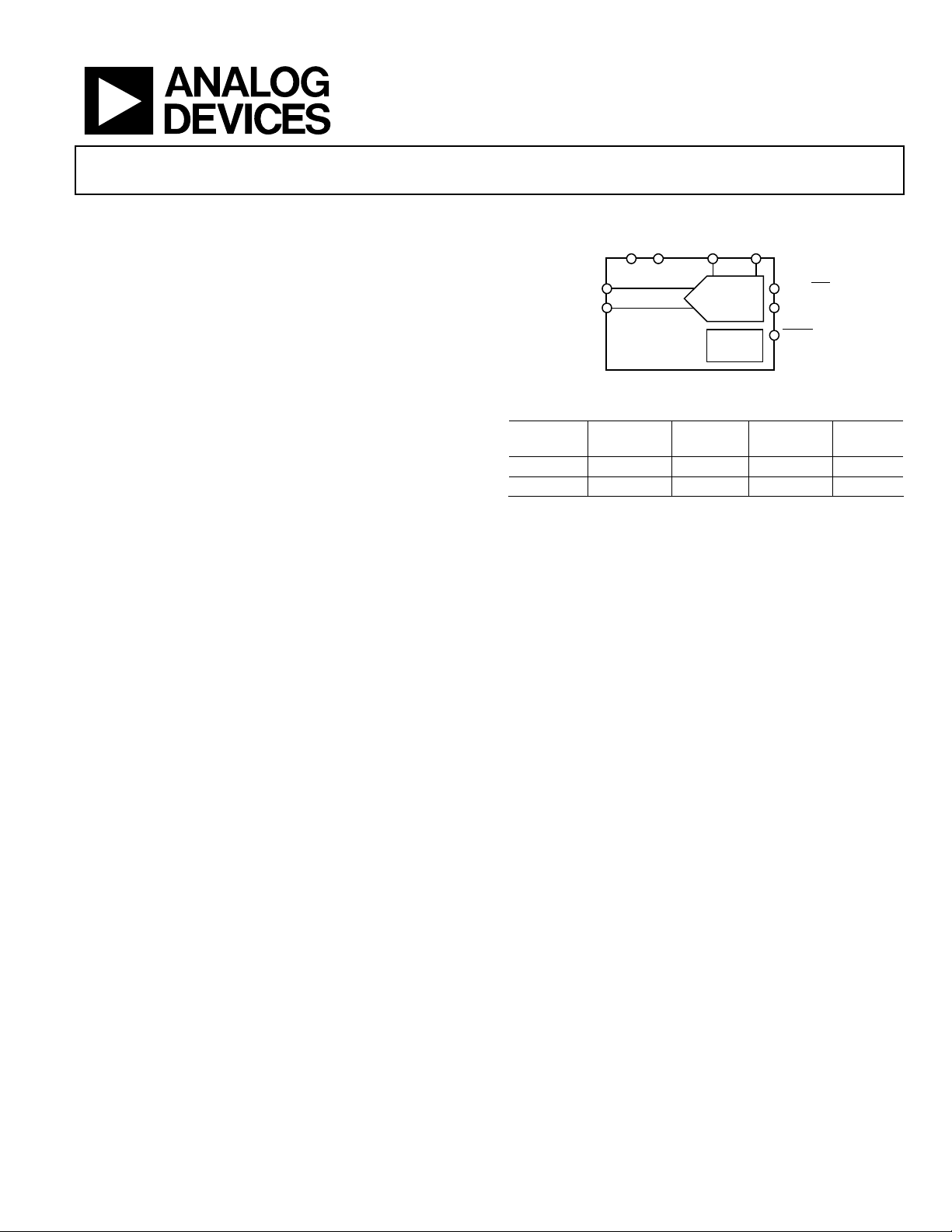
FUNCTIONAL BLOCK DIAGRAM
GND
IN(+)
AIN(–)
AD7170
Table 1.
V
= VDD RMS Noise P-P Noise
REF
5 V 11.5 V 76 V 12 bits 12 bits
3 V 6.9 V 45 V 12 bits 12 bits
The output data rate of the AD7170 is 125 Hz, whereas the
settling time is 24 ms. The AD7170 has one differential input
and a gain of 1. This is useful in applications where the user
needs to use an external amplifier to implement system-specific
filtering or gain requirements.
The AD7170 operates with a power supply from 2.7 V to 5.25 V.
It is available in a 10-lead LFCSP package.
The AD7171 is a 16-bit version of the AD7170. It has the same
feature set as the AD7170 and is pin-for-pin compatible.
DD
REFIN( +)
12-BIT Σ-∆
INTERNAL
Figure 1.
REFIN(–)
DOUT/ RDY
ADC
CLOCK
SCLK
PDRST
P-P
Resolution ENOB
08416-001
Rev. A
Information furnished by Analog Devices is believed to be accurate and reliable. However, no
responsibility is assumed by Anal og Devices for its use, nor for any infringements of patents or ot her
rights of third parties that may result from its use. Specifications subject to change without notice. No
license is granted by implication or otherwise under any patent or patent rights of Analog Devices.
Trademarks and registered trademarks are the property of their respective owners.
One Technology Way, P.O. Box 9106, Norwood, MA 02062-9106, U.S.A.
Tel: 781.329.4700 www.analog.com
Fax: 781.461.3113 ©2009–2011 Analog Devices, Inc. All rights reserved.

AD7170 Data Sheet
TABLE OF CONTENTS
Features.............................................................................................. 1
Interface ............................................................................................. 1
Applications....................................................................................... 1
Functional Block Diagram .............................................................. 1
General Description ......................................................................... 1
Revision History ............................................................................... 2
Specifications..................................................................................... 3
Timing Characteristics..................................................................... 5
Timing Diagrams.......................................................................... 5
Absolute Maximum Ratings............................................................ 6
Thermal Resistance ...................................................................... 6
ESD Caution.................................................................................. 6
Pin Configuration and Function Descriptions............................. 7
Typical Performance Characteristics ............................................. 8
Output Noise and Resolution Specifications ................................ 9
ADC Circuit Information.............................................................. 10
Overview ..................................................................................... 10
Filter, Data Rate, and Settling Time......................................... 10
Gain.............................................................................................. 10
Power-Down/Reset (
Analog Input Channel............................................................... 10
Bipolar Configuration................................................................ 10
Data Output Coding .................................................................. 11
Reference ..................................................................................... 11
Digital Interface.......................................................................... 11
Grounding and Layout.............................................................. 12
Applications Information.............................................................. 13
Temperature System................................................................... 13
Signal Conditioning Circuit...................................................... 13
Outline Dimensions....................................................................... 14
Ordering Guide .......................................................................... 14
PDRST
) ................................................... 10
REVISION HISTORY
9/11—Rev. 0 to Rev. A
Changes to Digital Interface Section............................................ 11
Updated Outline Dimensions....................................................... 14
Changes to Ordering Guide.......................................................... 14
10/09—Revision 0: Initial Version
Rev. A | Page 2 of 16

Data Sheet AD7170
SPECIFICATIONS
VDD = 2.7 V to 5.25 V, V
Table 1.
Parameter
ADC CHANNEL
Output Data Rate (f
No Missing Codes2 12 Bits
Noise Free Resolution 12 Bits V
Resolution Peak-to-Peak (p-p) 12 Bits V
Effective Resolution (ENOB) 12 Bits V
RMS Noise See Table 6 V V
Integral Nonlinearity ±0.1 LSB
Offset Error ±200
Offset Error Drift vs. Temperature ±250 nV/°C
Full-Scale Error ±0.015 % of FS
Gain Drift vs. Temperature ±0.07 LSB/°C
Power Supply Rejection 85 dB V
ANALOG INPUTS
Differential Input Voltage Range ±V
Absolute AINx Voltage Limits2 GND − 0.03 VDD + 0.03 V
Average Input Current2 ±400 nA/V
Average Input Current Drift ±60 pA/V/°C
DC Common-Mode Rejection 90 dB V
REFERENCE
External REFIN Voltage VDD V REFIN = REFIN(+) − REFIN(−)
Reference Voltage Range2 0.5 VDD V
Absolute REFIN Voltage Limits2 GND − 0.03 V
Average Reference Input Current 400 nA/V
Average Reference Input Current
Drift
DC Common-Mode Rejection 110 dB
INTERNAL CLOCK
Frequency2 64 − 5% 64 + 5% kHz
LOGIC INPUTS
SCLK, PDRST2
Input Low Voltage, V
0.8 V VDD = 5 V
Input High Voltage, V
2.4 V VDD = 5 V
SCLK (Schmitt-Triggered Input)2
Hysteresis 100 mV VDD = 3 V
140 mV VDD = 5 V
Input Currents ±2 µA VIN = VDD or GND
Input Capacitance 5 pF All digital inputs
= VDD, GND = 0 V, all specifications T
REF
MIN
to T
, unless otherwise noted.
MAX
AD7170B1
Min Typ Max
) 125 Hz Settling time = 3/f
ADC
V V
REF
Unit Test Conditions/Comments
= 0 V, V
INx
= 0 V, V
INx
= 0 V, V
INx
= 0 V, V
INx
μV
= 1 V
INx
= REFIN(+) − REFIN(−)
REF
Input current varies with input
voltage
= 1 V
INx
+ 0.03 V
DD
±0.15 nA/V/°C
0.4 V VDD = 3 V
INL
1.8 V VDD = 3 V
INH
REF
REF
REF
REF
= VDD
= VDD
= VDD
= VDD
ADC
Rev. A | Page 3 of 16

AD7170 Data Sheet
AD7170B1
Parameter
LOGIC OUTPUT (DOUT/RDY)
Output High Voltage, V
OH
2
V
Min Typ Max
− 0.6 V VDD = 3 V, I
DD
4 V VDD = 5 V, I
Output Low Voltage, V
2
0.4 V VDD = 3 V, I
OL
0.4 V VDD = 5 V, I
Floating-State Leakage Current ±2 µA
Floating-State Output
5 pF
Capacitance
Data Output Coding Offset binary
POWER REQUIREMENTS3
Power Supply Voltage
VDD – GND 2.7 5.25 V
Power Supply Currents
IDD Current 110 130 µA VDD = 3 V
135 150 µA VDD = 5 V
IDD (Power-Down/Reset Mode) 5 µA
1
Temperature range is –40°C to +105°C.
2
Specification is not production tested but is supported by characterization data at initial product release.
3
Digital inputs equal to VDD or GND.
Unit Test Conditions/Comments
= 100 µA
SOURCE
= 200 µA
SOURCE
= 100 µA
SINK
= 1.6 mA
SINK
Rev. A | Page 4 of 16
Data Sheet AD7170
TIMING CHARACTERISTICS
VDD = 2.7 V to 5.25 V, GND = 0 V, Input Logic 0 = 0 V, Input Logic 1 = VDD, unless otherwise noted.
Table 2.
Parameter
1, 2
Limit at T
MIN
, T
Unit Conditions/Comments
MAX
READ
t1 100 ns min SCLK high pulse width
t2 100 ns min SCLK low pulse width
3
t
0 ns min SCLK active edge to data valid delay4
3
60 ns max VDD = 4.75 V to 5.25 V
80 ns max VDD = 2.7 V to 3.6 V
t4 10 ns min
SCLK inactive edge to DOUT/RDY
high
RESET
t5 100 ns min
t6 25 ms typ
1
Sample tested during initial release to ensure compliance. All input signals are specified with tR = tF = 5 ns (10% to 90% of VDD) and timed from a voltage level of 1.6 V.
2
See Figure 3.
3
These numbers are measured with the load circuit shown in Figure 2 and defined as the time required for the output to cross the VOL or VOH limits.
4
SCLK active edge is the falling edge of SCLK.
low pulse width
PDRST
high to data valid delay
PDRST
I
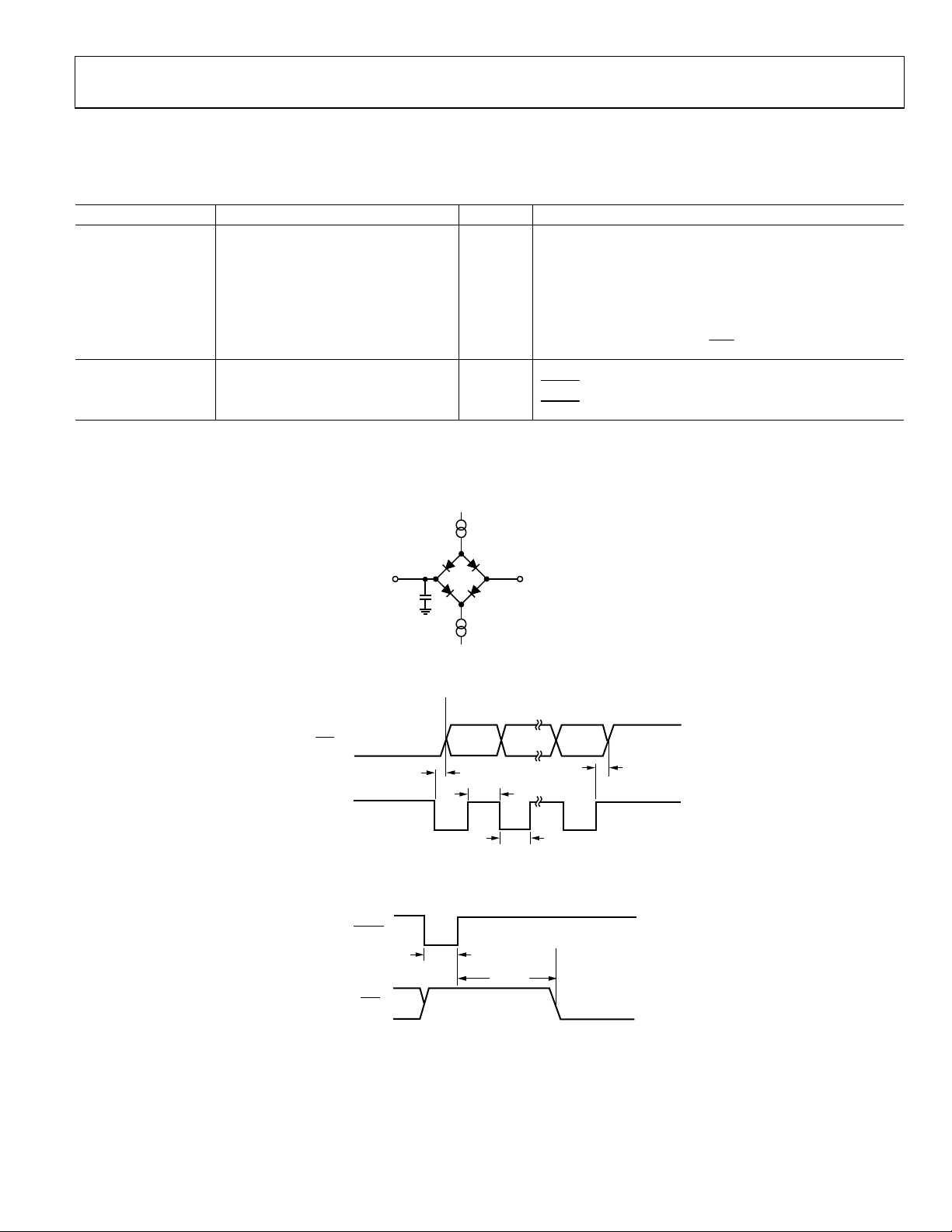
(1.6mA WITH VDD = 5V,
SINK
100µA WIT H V
TO
OUTPUT
PIN
50pF
I
SOURCE
100µA WIT H V
Figure 2. Load Circuit for Timing Characterization
= 3V)
DD
1.6V
(200µA WIT H VDD = 5V,
= 3V)
DD
08416-002
TIMING DIAGRAMS
DOUT/RDY (O )
SCLK (I)
DOUT/RDY (O )
MSB LSB
t
3
I = INPUT, O = OUTPUT
Figure 3. Read Cycle Timing Diagram
PDRST (I)
t
5
I = INPUT, O = OUTPUT
Figure 4. Resetting the AD7170
t
4
t
1
t
2
08416-003
t
6
08416-004
Rev. A | Page 5 of 16
AD7170 Data Sheet
ABSOLUTE MAXIMUM RATINGS
TA = 25°C, unless otherwise noted.
Table 3.
Parameter Rating
VDD to GND −0.3 V to +7 V
Analog Input Voltage to GND −0.3 V to VDD + 0.3 V
Reference Input Voltage to GND −0.3 V to VDD + 0.3 V
Digital Input Voltage to GND −0.3 V to VDD + 0.3 V
Digital Output Voltage to GND −0.3 V to VDD + 0.3 V
V
/Digital Input Current 10 mA
INx
Operating Temperature Range −40°C to +105°C
Storage Temperature Range −65°C to +150°C
Maximum Junction Temperature 150°C
Lead Temperature, Soldering
Reflow 260°C
Stresses above those listed under Absolute Maximum Ratings
may cause permanent damage to the device. This is a stress
rating only; functional operation of the device at these or any
other conditions above those indicated in the operational
section of this specification is not implied. Exposure to absolute
maximum rating conditions for extended periods may affect
device reliability.
THERMAL RESISTANCE
θJA is specified for the worst-case conditions, that is, a device
soldered in a circuit board for surface-mount packages.
Table 4.
Package Type θJA θ
LFCSP 48.7 2.96 °C/W
Unit
JC
ESD CAUTION
Rev. A | Page 6 of 16
Data Sheet AD7170
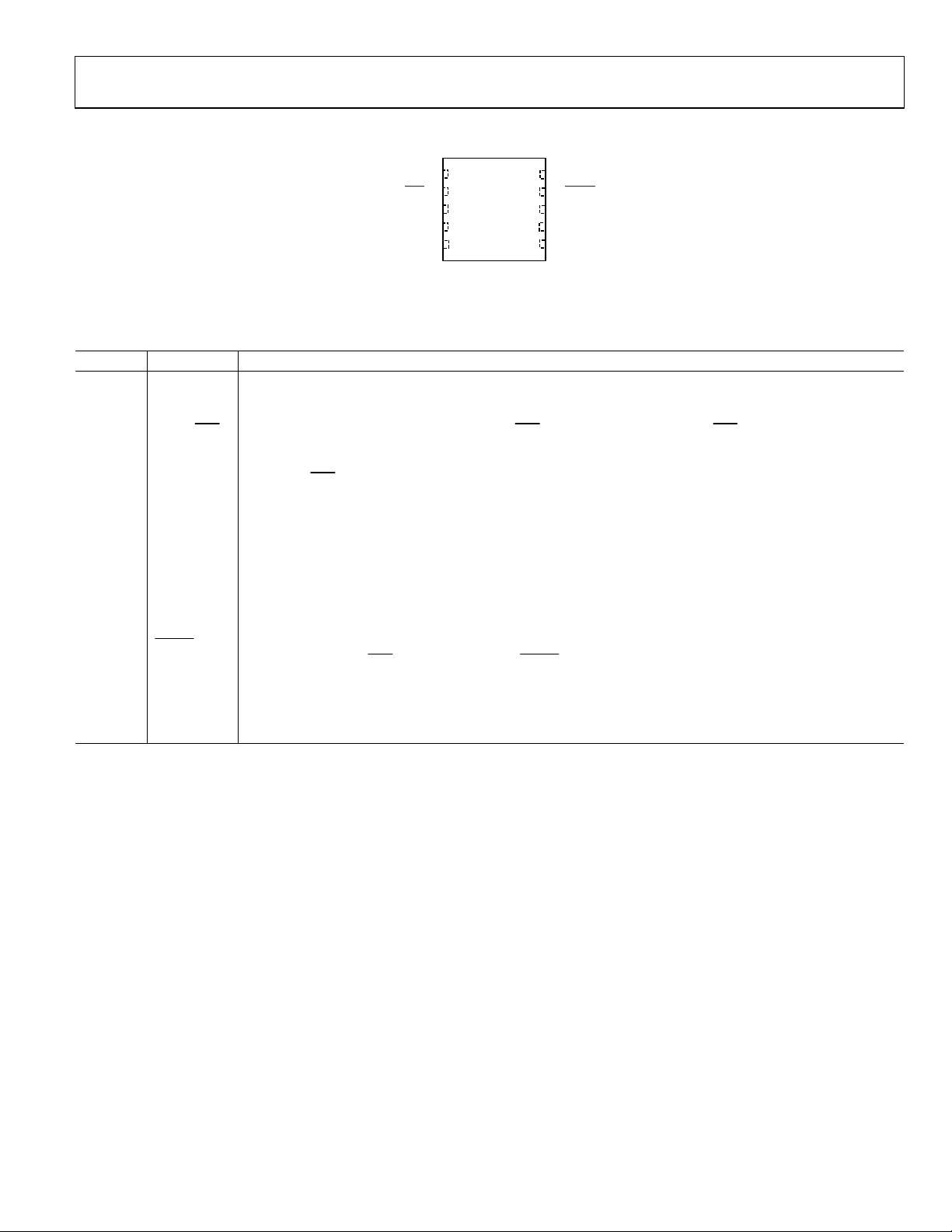
PIN CONFIGURATION AND FUNCTION DESCRIPTIONS
1SCLK
AD7170
2DOUT/RDY
3AIN(+)
TOP VIEW
(Not to Scal e)
4AIN(–)
5REFIN(+)
NOTES
1. NC = NO CONNECT.
2. CONNECT EXPOSED PAD TO GROUND.
Figure 5. Pin Configuration
10 NC
9 PDRST
8V
DD
7GND
6REFIN(–)
8416-005
Table 5. Pin Function Descriptions
Pin No. Mnemonic Description
1 SCLK
Serial Clock Input. This serial clock input is for data transfers from the ADC. The SCLK has a Schmitt-triggered
input. The serial clock can be continuous with all data transmitted in a constant train of pulses. Alternatively, it
can be a noncontinuous clock with the information being transmitted from the ADC in smaller batches of data.
2
DOUT/RDY
Serial Data Output/Data Ready Output. DOUT/RDY serves a dual purpose. DOUT/RDY operates as a data ready
pin, going low to indicate the completion of a conversion. In addition, it functions as a serial data output pin to
access the data register of the ADC. Eight status bits accompany each data read. See for further details.
The DOUT/
RDY
falling edge can be used as an interrupt to a processor, indicating that new data is available. If
Figure 13
the data is not read after the conversion, the pin goes high before the next update occurs.
3 AIN(+) Analog Input. AIN(+) is the positive terminal of the differential analog input pair AIN(+)/AIN(−).
4 AIN(−) Analog Input. AIN(−) is the negative terminal of the differential analog input pair AIN(+)/AIN(−).
5 REFIN(+)
Positive Reference Input. An external reference can be applied between REFIN(+) and REFIN(–). The nominal
reference voltage (REFIN(+) – REFIN(−)) is 5 V, but the part can function with a reference of 0.5 V to V
6 REFIN(−) Negative Reference Input.
7 GND Ground Reference Point.
8 VDD Supply Voltage, 2.7 V to 5.25 V.
9
Power-Down/Reset. When this pin is low, the ADC is placed in power-down mode. All the logic on the chip is
PDRST
reset, and the DOUT/RDY
pin is tristated. When PDRST is high, the ADC is taken out of power-down mode. The
on-chip clock powers up and settles, and the ADC continuously converts. The internal clock requires 1 ms
approximately to power up.
10 NC This pin should be connected to GND for correct operation.
EPAD Connect the exposed pad to ground.
.
DD
Rev. A | Page 7 of 16
AD7170 Data Sheet
TYPICAL PERFORMANCE CHARACTERISTICS
10
= VDD = 5V
V
REF
8
V
= VDD = 3V
REF
6
0.025
0.023
0.021
4
RMS NOISE (µV)
2
0
–40 –10 20 50 80 110
TEMPERATURE (°C)
Figure 6. AD7170 RMS Noise vs. Temperature
0.020
0.015
0.010
0.005
0
INL (LSB)
–0.005
–0.010
–0.015
–3 3210–1–2
Figure 7. Integral Nonlinearity (V
180
160
OFFSET (µV)
140
120
–40 –10 20 50 80 110
VIN (V)
TEMPERATURE (°C)
= VDD)
REF
Figure 8. Offset vs. Temperature
0.019
GAIN ERROR (%)
0.017
0.015
–40 –10 20 50 80 110
08416-015
TEMPERATURE (°C)
08416-008
Figure 9. Gain Error vs. Temperature
140
132
124
(µA)
DD
I
116
108
100
–40 –10 20 50 80 110
08416-006
V
= VDD = 5V
REF
V
= VDD = 3V
REF
TEMPERATURE (°C)
08416-016
Figure 10. Power Supply Current vs. Temperature
4.5
4.0
3.5
3.0
2.5
(µA)
DD
2.0
I
1.5
1.0
0.5
0
–40 –10 20 50 80 110
08416-007
V
= VDD = 5V
REF
V
= VDD = 3V
REF
TEMPERATURE (°C)
08416-017
Figure 11. Power-Down Current vs. Temperature
Rev. A | Page 8 of 16

Data Sheet AD7170
OUTPUT NOISE AND RESOLUTION SPECIFICATIONS
Tabl e 6 shows the rms noise of the AD7170. The numbers given
are for a 5 V and a 3 V reference. These numbers are typical and
are generated with a differential input voltage of 0 V. The
corresponding p-p resolution is also listed, along with the
effective resolution (ENOB). It is important to note that the
effective resolution is calculated using the rms noise, whereas
the p-p resolution is based on the p-p noise. The p-p resolution
represents the resolution for which there is no code flicker.
These numbers are typical.
The effective number of bits (ENOB) is defined as
ENOB = ln (FSR/RMS noise)/ln(2)
The noise-free bits, or p-p resolution, are defined as
Noise-Free Bits = ln (FSR/Peak-to-Peak Noise)/ln(2)
where FSR is the full-scale range and is equal to 2 × V
Table 6. RMS Noise and Resolution of the AD7170
P-P
V
= VDD RMS Noise P-P Noise
REF
5 V 11.5 V 76 V 12 bits 12 bits
3 V 6.9 V 45 V 12 bits 12 bits
Resolution ENOB
REF
/gain.
Rev. A | Page 9 of 16

AD7170 Data Sheet
ADC CIRCUIT INFORMATION
OVERVIEW
The AD7170 is a low power ADC that incorporates a precision
12-bit Σ-∆ modulator and an on-chip digital filter intended for
measuring wide dynamic range, low frequency signals. The
device has an internal clock and one differential input. It
operates with an output data rate of 125 Hz and has a gain of 1.
A 2-wire interface simplifies data retrieval from the AD7170.
FILTER, DATA RATE, AND SETTLING TIME
The AD7170 uses a sinc3 filter. The output data rate is set to
125 Hz; thus, valid conversions are available every 1/125 = 8 ms.
If a reset occurs, then the user must allow the complete settling
time for the first conversion after the reset. The settling time is
equal to 24 ms. Subsequent conversions are available at 125 Hz.
When a step change occurs on the analog input, the AD7170
requires several conversion cycles to generate a valid conversion.
If the step change occurs synchronous to the conversion period,
then the settling time of the AD7170 must be allowed to generate
a valid conversion. If the step change occurs asynchronous to
the end of a conversion, then an extra conversion must be allowed
to generate a valid conversion. The data register is updated with
all the conversions but, for an accurate result, the user must
allow the required time.
Figure 12 shows the filter response of the filter. The only external
filtering required on the analog inputs is a simple R-C filter to
provide rejection at multiples of the master clock. A 1 K
resistor in series with each analog input, a 0.01 F capacitor
from each input to GND, and a 0.1 F capacitor from AIN(+) to
AIN(−) are recommended.
0
–10
–20
–30
–40
–50
–60
FILTER GAIN (dB)
–70
–80
–90
–100
0625500375250125
INPUT SIGNAL FREQUENCY (Hz)
Figure 12. Filter Response
750
08416-011
POWER-DOWN/RESET(PDRST)
PDRST
The
When
pin functions as a power-down pin and a reset pin.
PDRST
is taken low, the AD7170 is powered down. The
entire ADC is powered down (including the on-chip clock), and
the DOUT/
RDY
pin is tristated. The circuitry and serial interface
are also reset. This resets the logic, the digital filter, and the analog
modulator.
PDRST
must be held low for 100 ns minimum to
initiate the reset function (see ). Figure 4
PDRST
When
is taken high, the AD7170 is taken out of powerdown mode. When the on-chip clock has powered up (1 ms,
typically), the modulator then begins sampling the analog input.
The DOUT/
RDY
pin becomes active, going high until a valid
conversion is available. A reset is automatically performed on
power-up.
ANALOG INPUT CHANNEL
The AD7170 has one differential analog input channel that is
connected to the modulator; that is, the input is unbuffered.
Note that this unbuffered input path provides a dynamic load
to the driving source. Therefore, resistor/capacitor combinations
on the input pins can cause dc gain errors, depending on the
output impedance of the source that is driving the ADC input.
Tabl e 7 shows the allowable external resistance/capacitance
values such that no gain error at the 12-bit level is introduced.
Table 7. External R-C Combination for No Gain Error
C (pF) R (Ω)
50 9 k
100 6 k
500 1.5 k
1000 900
5000 200
The absolute input voltage range is restricted to a range between
GND − 30 mV and V
+ 30 mV. Care must be taken in setting up
DD
the common-mode voltage to avoid exceeding these limits. Otherwise, there is degradation in linearity and noise performance.
BIPOLAR CONFIGURATION
The AD7170 accepts a bipolar input range. A bipolar input
range does not imply that the part can tolerate negative voltages
with respect to system GND. Signals on the AIN(+) input are
referenced to the voltage on the AIN(−) input. For example, if
AIN(−) is 2.5 V, the analog input range on the AIN(+) input is
0 V to 5 V when a 2.5 V reference is used.
GAIN
The AD7170 has a gain of 1. The acceptable analog input range
is +
V
. Therefore, with V
REF
= 5 V, the input range is +5 V.
REF
Rev. A | Page 10 of 16

Data Sheet AD7170
RDY
DATA OUTPUT CODING
The AD7170 uses offset binary coding. Therefore, a negative
full-scale voltage results in a code of 000...000, a zero differential
input voltage results in a code of 100...000, and a positive fullscale input voltage results in a code of 111...111. The output
code for any analog input voltage can be represented as
Code = 2
N – 1
× [(V
INx/VREF
) + 1]
where:
V
is the analog input voltage.
INx
N = 12 for the AD7170.
REFERENCE
The AD7170 has a fully differential input capability for the
channel. The common-mode range for these differential inputs
is GND to V
. The reference input is unbuffered; therefore,
DD
excessive R-C source impedances introduce gain errors. The
reference voltage REFIN (REFIN(+) − REFIN(−)) is V
DD
nominal, but the AD7170 is functional with reference voltages
of 0.5 V to V
. In applications where the excitation (voltage or
DD
current) for the transducer on the analog input also drives the
reference voltage for the part, the effect of the low frequency
noise in the excitation source is removed because the application
is ratiometric. If the AD7170 is used in a nonratiometric
application, a low noise reference should be used.
Recommended 2.5 V reference voltage sources for the AD7170
include the ADR381 and ADR391, which are low noise, low
power references. Also, note that the reference inputs provide
a high impedance, dynamic load. Because the input impedance
of each reference input is dynamic, resistor/capacitor combinations
on these inputs can cause dc gain errors, depending on the output
impedance of the source that is driving the reference inputs.
Reference voltage sources such as those recommended above
(the ADR391, for example) typically have low output
impedances and are, therefore, tolerant to decoupling capacitors
on REFIN(+) without introducing gain errors in the system.
Deriving the reference input voltage across an external resistor
means that the reference input sees a significant external source
impedance. External decoupling on the REFIN(±) pins is not
recommended in this type of circuit configuration.
DIGITAL INTERFACE
The serial interface of the AD7170 consists of two signals: SCLK
RDY
and DOUT/
and data transfers occur with respect to the SCLK signal. The
. SCLK is the serial clock input for the device,
DOUT/
pin and as a data out pin. DOUT/
data-word is available in the output register. A 24-bit word is
placed on the DOUT/
applied. This consists of a 12-bit conversion result followed by
four 0s to generate a 16-bit word. Following this, eight status
bits are output. shows the functions of the status bits. Tabl e 8
RDY
is available.
0: This bit is set to 0.
ERR: This bit is set to 1 if an error occurred during the conver-
sion. An error occurs when the analog input is outside range.
ID1, ID0: ID bits. These bits indicate the ID number for the
AD7170. Bit ID1 and Bit ID0 are set to 0 for the AD7170.
PAT2, PAT1, PAT0: status pattern bits. They are set to 101 by
default. When the user reads the data from the AD7170, a
pattern check can be performed. If the PAT2 to PAT0 bits are
different from their default values, the serial transfer from the
ADC was not performed correctly.
Table 8. Status Bits
RDY
DOUT/
conversion is not read, DOUT/
register update to indicate when not to read from the device.
This ensures that a read operation is not attempted while the
register is being updated. Each conversion can be read only
once. The data register is updated for every conversion. So,
when a conversion is complete, the serial interface is reset, and
the new conversion is placed in the data register. Therefore, the
user must ensure that the complete word is read before the next
conversion is complete.
When
PDRST
imately, to power up. Following this, the ADC continuously
converts. The first conversion requires the complete settling
time (see ). DOUT/Figure 4
taken high and returns low only when a conversion is available.
The ADC then converts continuously, subsequent conversions
being available at 125 Hz. shows the timing for a read
operation from the AD7170.
pin is dual purpose: it functions as a data ready
RDY
goes low when a new
RDY
pin when sufficient SCLK pulses are
: ready bit. This bit is set low to indicate that a conversion
0 ERR ID1 ID0 PAT2 PAT1 PAT0
RDY
is reset high when the conversion is read. If the
RDY
goes high prior to the data
PDRST
is low, the DOUT/
RDY
pin is tristated. When
is taken high, the internal clock requires 1 ms, approx-
RDY
goes high when
PDRST
is
Figure 3
Rev. A | Page 11 of 16

AD7170 Data Sheet
GROUNDING AND LAYOUT
Because the analog input and reference input of the ADC are
differential, most of the voltages in the analog modulator are
common-mode voltages. The excellent common-mode rejection of the part removes common-mode noise on these inputs.
The digital filter provides rejection of broadband noise on the
power supply, except at integer multiples of the modulator
sampling frequency. The digital filter also removes noise from
the analog and reference inputs provided that these noise sources
do not saturate the analog modulator. As a result, the AD7170
is more immune to noise interference than conventional high
resolution converters. However, because the noise levels from
the AD7170 are so low, care must be taken with regard to
grounding and layout.
The printed circuit board that houses the AD7170 should be
designed such that the analog and digital sections are separated
and confined to certain areas of the board. A minimum etch
technique is generally best for ground planes because it gives
the best shielding.
It is recommended that the GND pin of the AD7170 be tied to
the analog ground (AGND) plane of the system. In any layout,
it is important that the user pay attention to the flow of currents
in the system and ensure that the return paths for all currents
are as close as possible to the paths the currents took to reach
their destinations. Avoid forcing digital currents to flow through
the AGND sections of the layout.
The ground plane of the AD7170 should be allowed to run
under the AD7170 to prevent noise coupling. The power supply
lines to the AD7170 should use as wide a trace as possible to
provide low impedance paths and reduce the effects of glitches
on the power supply line. Fast switching signals such as clocks
should be shielded with digital ground to avoid radiating noise
to other sections of the board, and clock signals should never be
run near the analog inputs. Avoid crossover of digital and
analog signals. Traces on opposite sides of the board should run
at right angles to each other. This reduces the effects of
feedthrough through the board. A microstrip technique is by far
the best, but it is not always possible with a double-sided board.
In this technique, the component side of the board is dedicated
to ground planes, while signals are placed on the solder side.
Good decoupling is important when using high resolution ADCs.
V
should be decoupled with 10 μF tantalum capacitors in
DD
parallel with 0.1 μF capacitors to GND, with the system’s analog
ground to digital ground (DGND) connection being close to
the AD7170. To achieve the best results from these decoupling
components, they should be placed as close as possible to the
device, ideally right up against the device. All logic chips should
be decoupled with 0.1 μF ceramic capacitors to DGND.
Rev. A | Page 12 of 16

Data Sheet AD7170
V
APPLICATIONS INFORMATION
The AD7170 provides a low cost, high resolution analog-todigital function. Because the analog-to-digital function is
provided by a Σ- architecture, the part is more immune to
noisy environments, making it ideal for use in sensor measurement and industrial and process-control applications.
TEMPERATURE SYSTEM
Figure 13 shows the AD7170 used in a temperature measurement system. The thermistor is connected in series with a
precision resistor, R
generate the reference voltage. The value of R
maximum resistance produced by the thermistor. The complete
dynamic range of the ADC is then used, resulting in optimum
performance.
DD
R
REF
Figure 13. Temperature System Using the AD7170
, the precision resistor being used to
REF
REF
V
GND
AIN(+)
AIN(–)
DD
12-BIT Σ-∆
ADC
AD7170
REFIN(+)
REFIN(–)
INTERNAL
CLOCK
is equal to the
DOUT/RDY
SCLK
PDRST
08416-013
SIGNAL CONDITIONING CIRCUIT
Figure 14 shows the AD7170 used in a signal conditioning
circuit for a single-ended analog input. In a low side shunt
current monitor, a low resistance shunt resistor converts the
current to voltage. The resulting voltage is amplified and
applied to the AD7170.
32kΩ
1kΩ
ANALOG
INPUT
AD5041
AIN(+)
AD8631
1µF
AIN(–)
REFIN(+)
REFIN(–)
Figure 14. Signal Conditioning Circuit
GND V
DD
12-BIT
Σ-∆ ADC
INTERNAL
CLOCK
AD7170
DOUT/RDY
SCLK
08416-018
Rev. A | Page 13 of 16

AD7170 Data Sheet
OUTLINE DIMENSIONS
2.48
3.10
3.00 SQ
2.90
2.38
2.23
0.50 BSC
PIN 1 INDEX
AREA
0.80
0.75
0.70
SEATING
PLANE
TOP VIEW
0.30
0.25
0.20
0.50
0.40
0.30
0.05 MAX
0.02 NOM
0.20 REF
6
EXPOSED
PAD
5
BOTTOM VIEW
FOR PROPER CONNECTION OF
THE EXPOSED PAD, REFER TO
THE PIN CONFIGURATION AND
FUNCTION DESCRIPTIONS
SECTION OF THIS DATA SHEET.
10
1.74
1.64
1.49
1
N
1
P
I
R
C
I
A
O
T
N
I
D
)
5
1
.
R
0
(
121009-A
Figure 15. 10-Lead Lead Frame Chip Scale Package [LFCSP_WD]
3 mm × 3 mm Body, Very Very Thin, Dual Lead
(CP-10-9)
Dimensions shown in millimeters
ORDERING GUIDE
Temperature
Model1
AD7170BCPZ-REEL7 −40°C to +105°C 10-Lead Lead Frame Chip Scale Package [LFCSP_WD] CP-10-9 C6F
AD7170BCPZ-500RL7 −40°C to +105°C 10-Lead Lead Frame Chip Scale Package [LFCSP_WD] CP-10-9 C6F
EVAL-AD7170EBZ Evaluation Board
1
Z = RoHS Compliant Part.
Range Package Description Package Option Branding
Rev. A | Page 14 of 16

Data Sheet AD7170
NOTES
Rev. A | Page 15 of 16

AD7170 Data Sheet
NOTES
©2009–2011 Analog Devices, Inc. All rights reserved. Trademarks and
registered trademarks are the property of their respective owners.
D08416-0-9/11(A)
Rev. A | Page 16 of 16
 Loading...