

V
V
12-Bit Capacitance-to-Digital Converter
FEATURES
Capacitance-to-digital converters
Interfaces to floating sensors
Resolution down to 0.25 fF (that is, up to 12 ENOB)
Linearity: 0.05%
Common-mode (not changing) capacitance up to 5 pF
Four capacitance ranges selectable per operation mode
±0.25 pF to ±2 pF in differential mode
0.5 pF to 4 pF in single-ended mode
Tolerant of parasitic capacitance to ground up to 50 pF
Conversion time per channel: 5 ms, 20 ms, 50 ms, and 60 ms
Internal clock oscillator
2-wire serial interface (I
Power
2.7 V to 3.6 V single-supply operation
100 μA current consumption
Operating temperature: −40°C to +85°C
10-lead MSOP package
APPLICATIONS
Automotive, industrial, and medical systems for
Pressure measurement
Position sensing
Level sensing
Flowmeters
Humidity sensing
2
C-compatible)
AD7152/AD7153
GENERAL DESCRIPTION
The AD7152/AD7153 are 12-bit sigma-delta (Σ-Δ) capacitance-todigital converters (CDCs). The capacitance to be measured
is connected directly to the device inputs. The architecture
features inherent high resolution (12-bit no missing codes,
up to 12-bit effective resolution) and high linearity (±0.05%).
The AD7152/AD7153 have four capacitance input ranges per
operation mode, ±0.25 pF to ±2 pF in differential mode and
0.5 pF to 4 pF in single-ended mode.
The AD7152/AD7153 can accept up to 5 pF common-mode
capacitance (not changing), which can be balanced by a
programmable on-chip, digital-to-capacitance converter
(CAPDAC).
The AD7153 has one capacitance input channel, while the
AD7152 has two channels. Each channel can be configured
as single-ended or differential. The AD7152/AD7153 are
designed for floating capacitive sensors.
The AD7152/AD7153 have a 2-wire, I
interface. Both parts can operate with a single power supply
from 2.7 V to 3.6 V. They are specified over the temperature
range of −40°C to +85°C and are available in a 10-lead MSOP
package.
2
C®-compatible serial
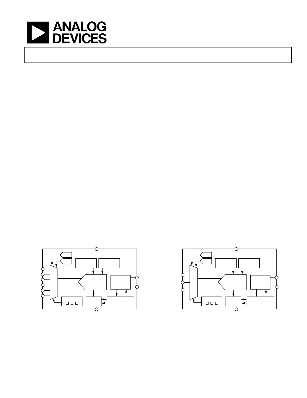
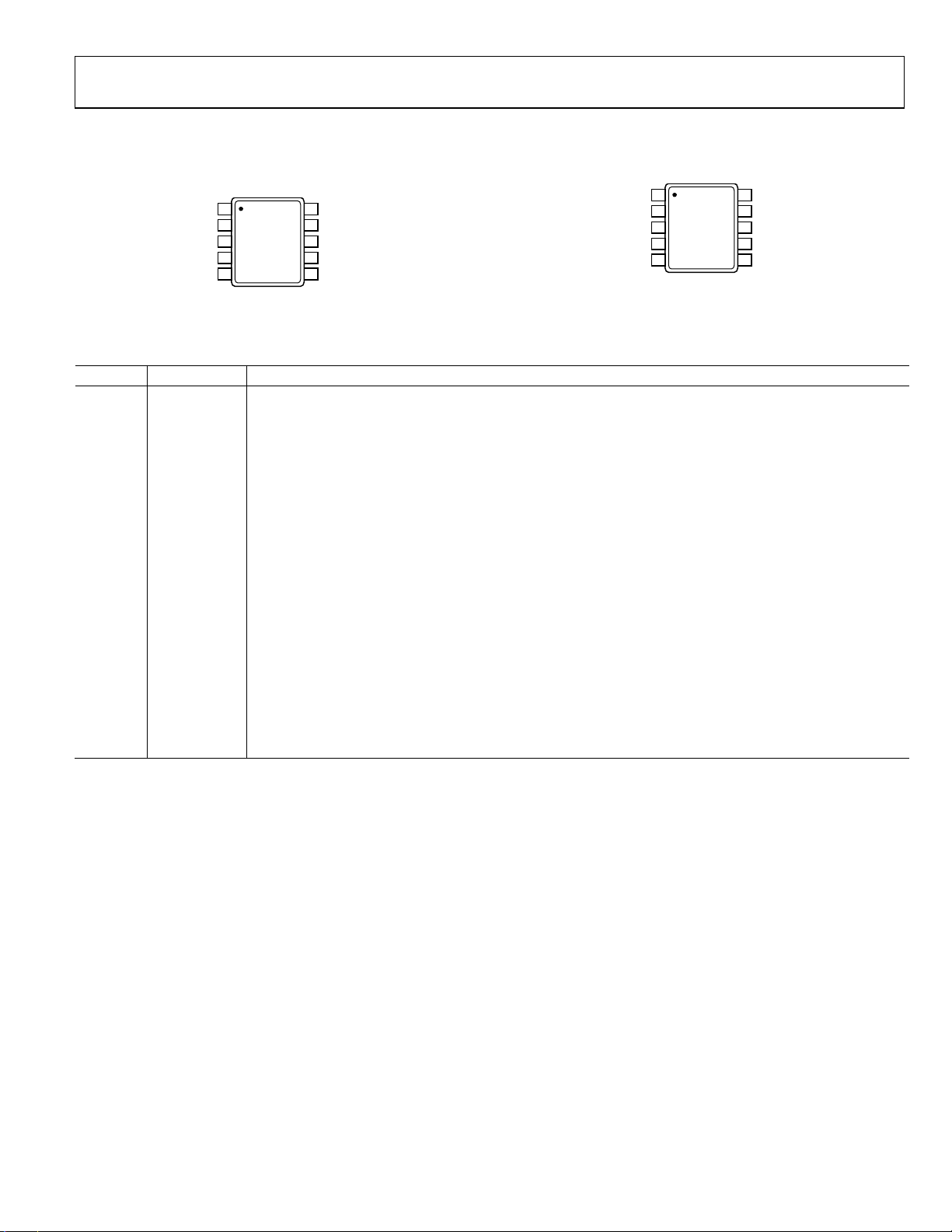
FUNCTIONAL BLOCK DIAGRAMS
DD
CAP+
CIN1(+)
CIN1(–)
EXC1
CIN2(+)
CIN2(–)
EXC2
MUX
CAP–
GENERATOR
EXCITATI ON
CLOCK
12-BIT Σ-Δ
MODULATOR
DIGITAL
FILTER
GND
VOLTAGE
REFERENCE
Figure 1.
Rev. 0
Information furnished by Analog Devices is believed to be accurate and reliable. However, no
responsibility is assumed by Anal og Devices for its use, nor for any infringements of p atents or other
rights of third parties that may result from its use. Specifications subject to change without notice. No
license is granted by implication or otherwise under any patent or patent rights of Analog Devices.
Trademarks and registered trademarks are the property of their respective owners.
AD7152
I2C
SERIAL
INTERFACE
CONTROL LOGIC
CALIBRATION
SDA
SCL
07450-001
DD
AD7153
I2C
SERIAL
INTERFACE
CONTROL LOGIC
CALIBRATION
CIN1(+)
CIN1(–)
EXC1
MUX
CAP+
CAP–
GENERATOR
EXCITATI ON
CLOCK
12-BIT Σ-Δ
MODULATOR
DIGITAL
FILTER
REFERENCE
GND
VOLTAGE
Figure 2.
One Technology Way, P.O. Box 9106, Norwood, MA 02062-9106, U.S.A.
Tel: 781.329.4700 www.analog.com
Fax: 781.461.3113 ©2008 Analog Devices, Inc. All rights reserved.
SDA
SCL
07450-002

AD7152/AD7153
TABLE OF CONTENTS
Features .............................................................................................. 1
Applications ....................................................................................... 1
General Description ......................................................................... 1
Functional Block Diagrams ............................................................. 1
Revision History ............................................................................... 2
Specifications ..................................................................................... 3
Timing Specifications .................................................................. 5
Absolute Maximum Ratings ............................................................ 6
ESD Caution .................................................................................. 6
Pin Configurations and Function Descriptions ........................... 7
Typical Performance Characteristics ............................................. 8
Serial Interface ................................................................................ 11
Write Operation .......................................................................... 11
Read Operation ........................................................................... 11
AD7152/AD7153 Reset ............................................................. 12
General Call................................................................................. 12
Register Map .................................................................................... 13
Status Register ............................................................................. 14
Data Registers ............................................................................. 15
Offset Calibration Registers ...................................................... 15
Gain Calibration Registers ........................................................ 15
CAP Setup Registers .................................................................. 16
Configuration Register .............................................................. 16
CAPDAC POS Register ............................................................. 17
CAPDAC NEG Register ............................................................ 17
Configuration2 Register ............................................................ 17
Circuit Description......................................................................... 18
Capacitance-to-Digital Converter (CDC) .............................. 18
Excitation Source ........................................................................ 18
CAPDAC ..................................................................................... 19
Single-Ended Capacitive Input ................................................. 19
Differential Capacitive Input .................................................... 20
Parasitic Capacitance to Ground .............................................. 20
Parasitic Resistance to Ground ................................................. 20
Parasitic Parallel Resistance ...................................................... 21
Parasitic Serial Resistance ......................................................... 21
Input EMC Protection ............................................................... 21
Power Supply Decoupling and Filtering .................................. 21
Capacitive Gain Calibration ..................................................... 21
Capacitive System Offset Calibration ...................................... 21
Typical Application Diagram .................................................... 22
Outline Dimensions ....................................................................... 23
Ordering Guide .......................................................................... 23
REVISION HISTORY
5/08—Revision 0: Initial Version
Rev. 0 | Page 2 of 24
AD7152/AD7153
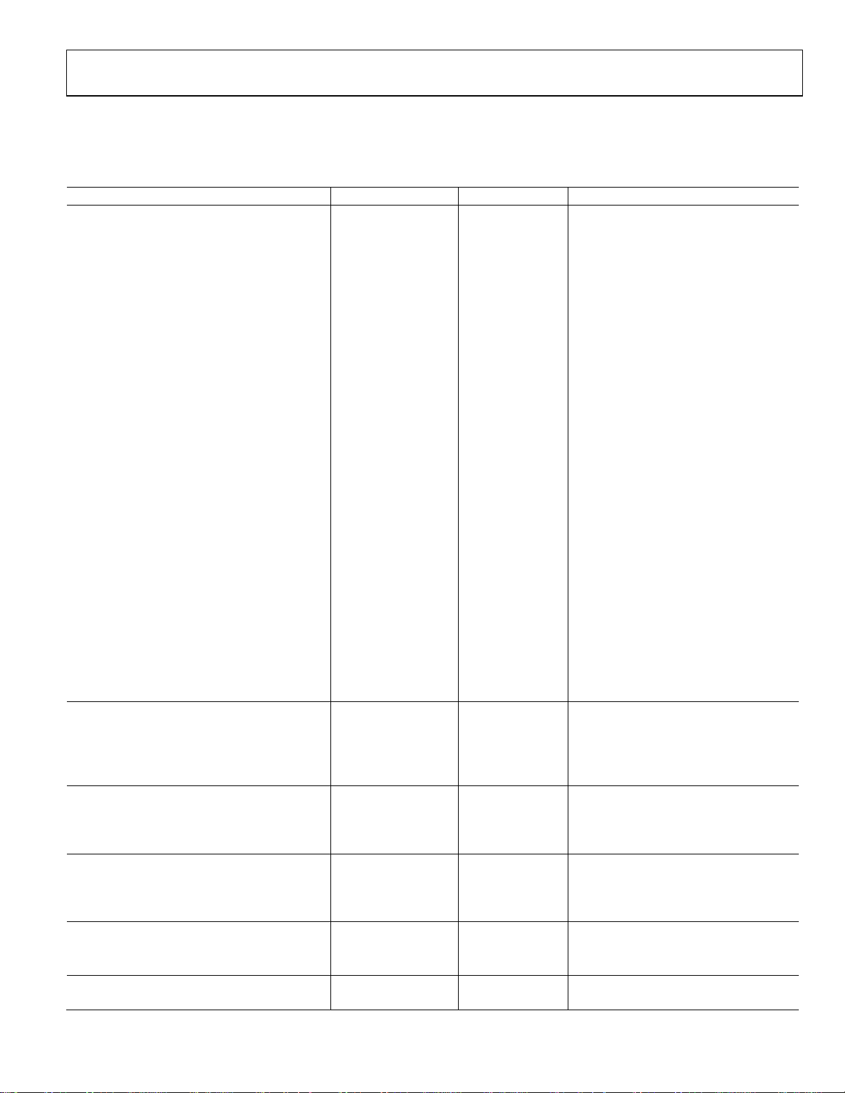
SPECIFICATIONS
VDD = 2.7 V to 3.6 V; GND = 0 V; −40°C to +85°C, unless otherwise noted.
Table 1.
Parameter Min Typ Max Unit
CAPACITIVE INPUT
Capacitive Input Ranges ±2 pF Differential mode
±1 pF
±0.5 pF
±0.25 pF
4 pF Single-ended mode
2 pF
1 pF
0.5 pF
Gain Matching Between Ranges ±3 % of FS
Integral Nonlinearity (INL)
No Missing Codes
Resolution, p-p
2
2, 3
10 Bits 25°C, V
Resolution Effective
Absolute Error
4
System Offset Calibration Range
Offset Deviation over Temperature
2
12 Bits
2, 3
12 Bits 25°C, V
±0.05 % of FS
±20 fF
5, 6
40 % of FSR
2
1 5 fF
0.3 1 fF
Gain Error
Gain Deviation over Temperature
Allowed Capacitance, CIN to GND
Allowed Resistance, CIN to GND
Allowed Serial Resistance
7
2
0.3 0.4 % of FSR See Figure 7
2
50 pF See Figure 9 and Figure 10
2
10 MΩ See Figure 13
2
20 kΩ See Figure 16
0.5 % of FSR 25°C, VDD = 3.3 V
Power Supply Rejection DC 2 fF/V See Figure 17
Normal-Mode Rejection
2
−70 dB 50 Hz ± 1 Hz, conversion time = 60 ms
−70 dB 60 Hz ± 1 Hz, conversion time = 50 ms
Channel-to-Channel Isolation
2
−70 dB AD7152 only
CAPDAC
Full Range 5 6.25 pF
Resolution
Differential Nonlinearity (DNL)
Offset Deviation over Temperature
8
2
0.25 LSB See Figure 18 and Figure 19
2
0.3 % of CAPDAC FSR Single-ended mode
200 fF 5-bit CAPDAC
EXCITATION
Frequency 30.9 32 32.8 kHz
Voltage ±VDD/2 V
Allowed Capacitance, EXC to GND
2
300 pF See Figure 11 and Figure 12
SERIAL INTERFACE LOGIC INPUTS (SCL, SDA)
Input High Voltage, VIH 1.5 V
Input Low Voltage, VIL 0.8 V
Input Leakage Current (SCL) ±0.1 ±5 μA
OPEN-DRAIN OUTPUT (SDA)
Output Low Voltage, VOL 0.4 V
Output High Leakage Current, IOH 0.1 5 μA V
POWER SUPPLY MONITOR
Threshold Voltage, VDD 2.45 2.65 V
1
Test Conditions/Comments
= 3.3 V, 4 pF range
DD
= 3.3 V, 4 pF range
DD
25°C, V
= 3.3 V, after system offset
DD
calibration, ±2 pF range
Single-ended mode, CIN and EXC
pins disconnected, see Figure 8
Differential mode, CIN and EXC
pins disconnected
I
= −6.0 mA
SINK
= VDD
OUT
Rev. 0 | Page 3 of 24

AD7152/AD7153
Parameter Min Typ Max Unit
1
Test Conditions/Comments
POWER REQUIREMENTS
VDD-to-GND Voltage 2.7 3.6 V VDD = 3.3 V, nominal
Current, I
Current Power-Down Mode, I
9
100 120 μA
DD
9
1 5 μA Temperature ≤ 25°C
DD
3 10 μA Temperature = 85°C
1
Capacitance units: 1 pF = 10
2
Specification is not production tested but is supported by characterization data at initial product release.
3
Except Channel 2 in differential mode. To achieve the specified performance in differential mode, the I2C interface must be idle during the capacitance conversion to
prevent signal coupling from the SCL pin to the adjacent CIN2(−) pin.
4
Factory calibrated. The absolute error includes factory gain calibration error and integral nonlinearity error all at 25°C. At different temperatures, compensation for
gain drift over temperature is required.
5
Specification is not production tested but guaranteed by design.
6
A system offset calibration is effectively a conversion; therefore, the offset error is of the order of the conversion noise. This applies after calibration at the temperature,
−12
F; 1 fF = 10
−15
F; 1 aF = 10
−18
F.
capacitive input range, and applied VDD of interest. The capacitive input offset can be reduced using a system offset calibration. Large offsets should be removed using
CAPDACs.
7
The gain error is factory calibrated at 25°C. At different temperatures, compensation for gain drift over temperature is required.
8
The CAPDAC resolution is five bits in the actual CAPDAC full range. Using the on-chip offset calibration or adjusting the capacitive offset calibration register can
further reduce the CIN offset or the unchanging CIN component.
9
Digital inputs equal to VDD or GND.
Rev. 0 | Page 4 of 24
AD7152/AD7153
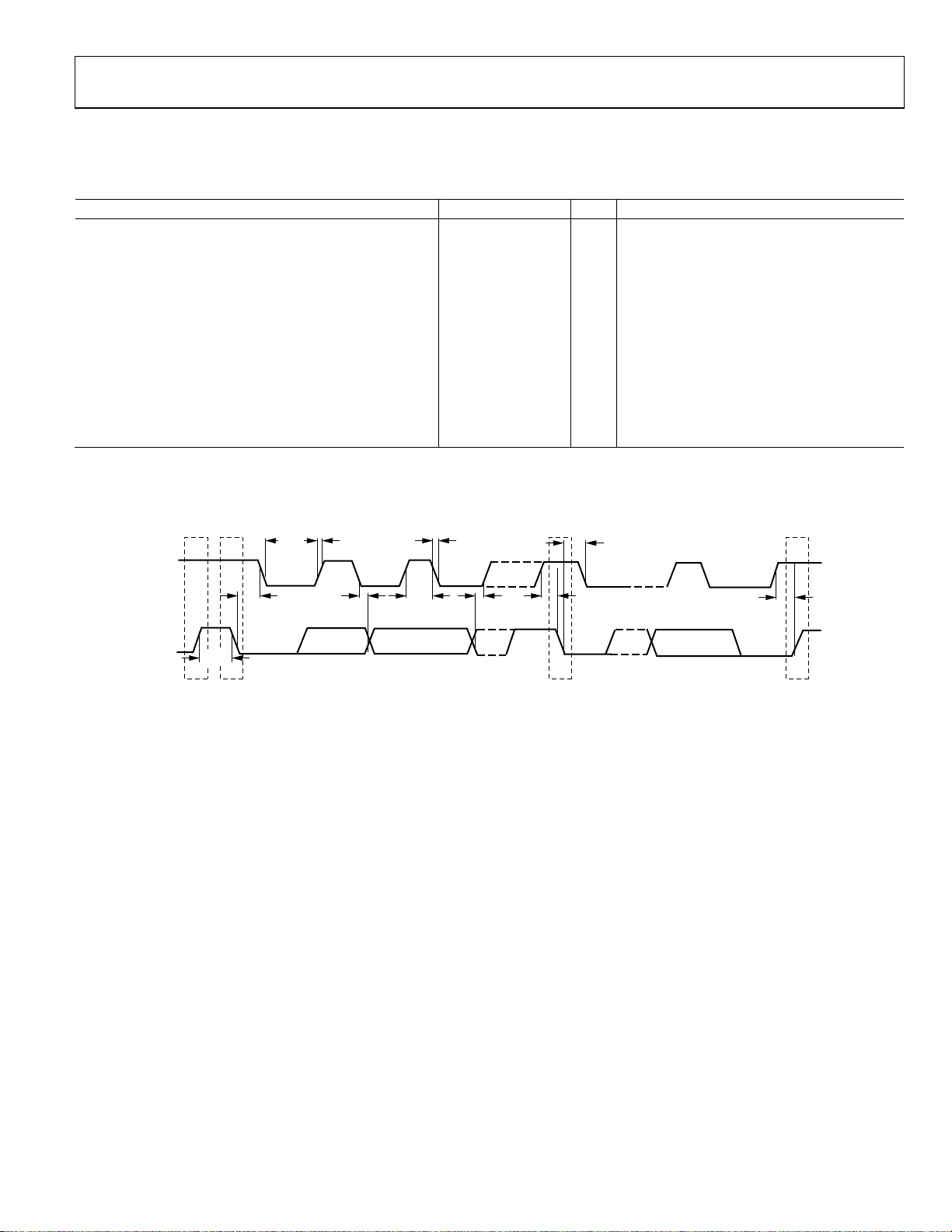
TIMING SPECIFICATIONS
VDD = 2.7 V to 3.6 V; GND = 0 V; Input Logic 0 = 0 V; Input Logic 1 = VDD; −40°C to +85°C, unless otherwise noted.
Table 2.
Parameter Min Typ Max Unit Test Conditions/Comments
SERIAL INTERFACE
SCL Frequency 0 400 kHz
SCL High Pulse Width, t
SCL Low Pulse Width, t
SCL, SDA Rise Time, tR 0.3 μs
SCL, SDA Fall Time, tF 0.3 μs
Hold Time (Start Condition), t
Set-Up Time (Start Condition), t
Data Set-Up Time, t
Setup Time (Stop Condition), t
Data Hold Time, t
Bus-Free Time (Between Stop and Start Conditions, t
1
Sample tested during initial release to ensure compliance.
2
All input signals are specified with input rise/fall times = 3 ns, measured between the 10% and 90% points. Timing reference points at 50% for inputs and outputs;
output load = 10 pF.
1, 2
0.6 μs
HIGH
1.3 μs
LOW
0.6 μs After this period, the first clock is generated.
HD;STA
0.6 μs Relevant for repeated start condition.
SU;STA
0.1 μs
SU;DAT
0.6 μs
SU;STO
(Master) 0.01 μs
HD;DAT
BUF
t
R
t
LOW
See Figure 3.
) 1.3 μs
t
F
t
HD;STA
SCL
SDA
t
HD;STA
t
BUF
PS
t
HD;DAT
t
HIGH
t
SU;DAT
Figure 3. Serial Interface Timing Diagram
t
SU;STA
S
t
SU;STO
P
07450-003
Rev. 0 | Page 5 of 24
AD7152/AD7153
ABSOLUTE MAXIMUM RATINGS
TA = 25°C, unless otherwise noted.
Table 3.
Parameter Rating
Positive Supply Voltage, VDD to GND −0.3 V to +3.9 V
Voltage on Any Input or Output Pin to GND −0.3 V to VDD + 0.3 V
ESD Rating (ESD Association Human
Body Model, S5.1)
ESD Rating (Field-Induced Charged
Device Model)
Operating Temperature Range −40°C to +85°C
Storage Temperature Range −65°C to +150°C
Junction Temperature 150°C
MSOP
θJA Thermal Impedance-to-Air 206°C/W
θJC Thermal Impedance-to-Case 44°C/W
Reflow Soldering (Pb-Free)
Peak Temperature 260 (+0/−5)°C
Time at Peak Temperature 10 sec to 40 sec
4 kV
750 V
Stresses above those listed under Absolute Maximum Ratings
may cause permanent damage to the device. This is a stress
rating only; functional operation of the device at these or any
other conditions above those indicated in the operational
section of this specification is not implied. Exposure to absolute
maximum rating conditions for extended periods may affect
device reliability.
ESD CAUTION
Rev. 0 | Page 6 of 24
AD7152/AD7153
PIN CONFIGURATIONS AND FUNCTION DESCRIPTIONS
GND
VDD
CIN1(–)
CIN1(+)
EXC2
1
2
AD7152
3
TOP VIEW
(Not to Scal e)
4
5
10
9
8
7
6
SDA
SCL
CIN2(–)
CIN2(+)
EXC1
07450-004
Figure 4. AD7152 Pin Configuration
Table 4. Pin Function Descriptions
Pin No. Mnemonic Description
1 GND Ground Pin.
2 VDD
Power Supply Voltage. This pin should be decoupled to GND, using a low impedance capacitor, for example, in
combination with a 10 μF tantalum and a 0.1 μF multilayer ceramic capacitor.
3 CIN1(–)
CDC Negative Capacitive Input of Channel 1. If not used, this pin can be left as an open circuit or connected to
GND. This pin is internally disconnected in single-ended CDC configuration.
4 CIN1(+)
5 EXC2/NC
CDC Positive Capacitive Input of Channel 1. If not used, this pin can be left as an open circuit or connected to GND.
AD7152: CDC Excitation Output for Channel 2. The measured capacitance is connected between one of the EXC
pins and one of the CIN pins. If not used, these pins should be left as an open circuit.
AD7153: No Connect. This pin must be left as an open circuit.
6 EXC1
CDC Excitation Output for Channel 1. The measured capacitance is connected between one of the EXC pins and
one of the CIN pins. If not used, these pins should be left as an open circuit.
7 CIN2(+)/NC
AD7152: CDC Positive Capacitive Input of Channel 2. If not used, this pin can be left as an open circuit or
connected to GND.
AD7153: No Connect. This pin must be left as an open circuit.
8 CIN2(–)/NC
AD7152: CDC Negative Capacitive Input of Channel 2. If not used, this pin can be left as an open circuit or
connected to GND. This pin is internally disconnected in single-ended CDC configuration.
AD7153: No Connect. This pin must be left as an open circuit.
9 SCL
Serial Interface Clock Input. Connects to the master clock line. Requires a pull-up resistor if one is not already
provided in the system.
10 SDA
Serial Interface Bidirectional Data. Connects to the master data line. Requires a pull-up resistor if one is not
provided elsewhere in the system.
GND
VDD
CIN1(–)
CIN1(+)
NC
1
2
AD7153
3
TOP VIEW
(Not to Scal e)
4
5
NC = NO CONNECT
10
SDA
SCL
9
NC
8
7
NC
6
EXC1
Figure 5. AD7153 Pin Configuration
07450-005
Rev. 0 | Page 7 of 24
AD7152/AD7153
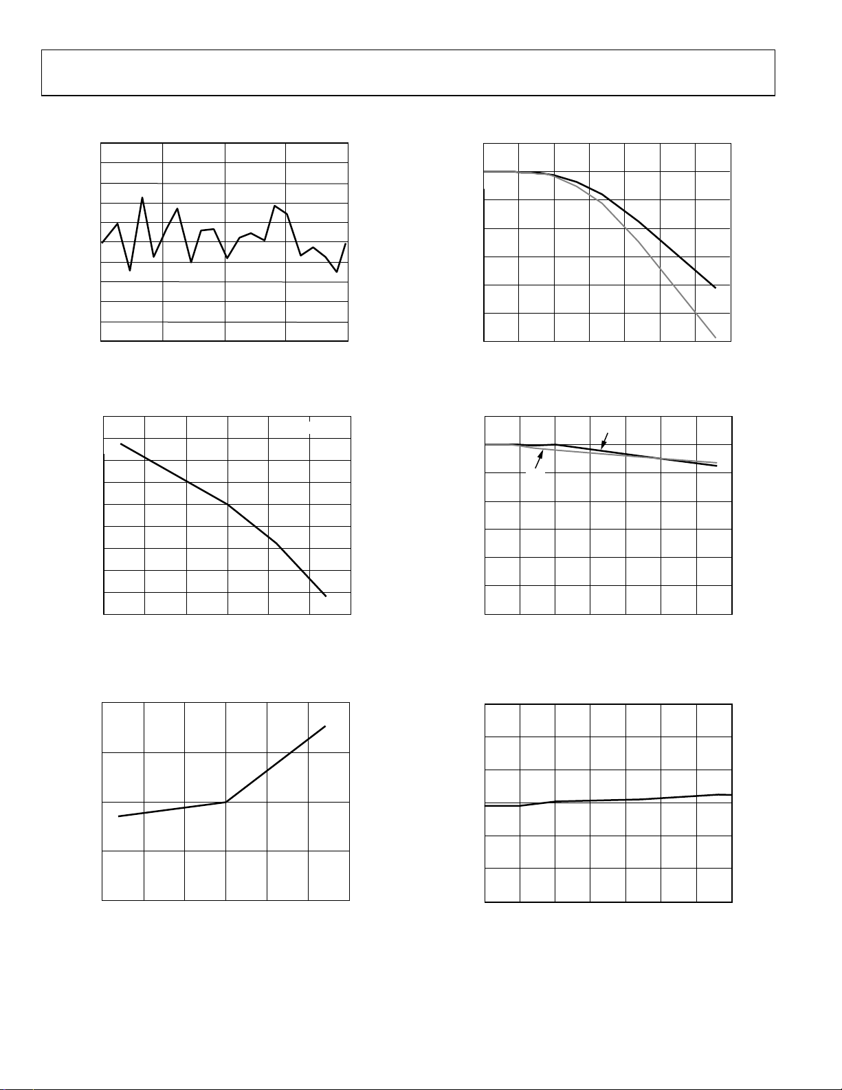
TYPICAL PERFORMANCE CHARACTERISTICS
0.05
0.04
0.03
0.02
0.01
0
0.01
INL (% of FSR)
0.02
0.03
0.04
0.05
–2 –1 0 1 2
CAPACITANCE (pF)
Figure 6. Capacitance Input Integral Nonlinearity,
= 3.3 V, See Figure 34
V
DD
0.20
0.15
0.10
0.05
0.00
–0.05
–0.10
GAIN ERROR (%FS R)
–0.15
–0.20
–0.25
50 25 0 25 50 75 100
TEMPERATURE (° C)
TC ≈ 28ppm/°C
Figure 7. Capacitance Input Gain Drift vs. Temperature,
V
= 3.3 V, Range = ±2 pF
DD
07450-106
07450-107
2
0
–2
–4
–6
GAIN ERROR (%F SR)
–8
–10
–12
0 50 100 150 200 250 300 350
CAP LOAD TO GND (pF)
9pF
3pF
07450-109
Figure 9. Capacitance Input Error vs. Capacitance Between CIN and GND;
Single-Ended Mode, CIN(+) to EXC = 3 pF and 9 pF, V
2
0
–2
–4
–6
GAIN ERROR (%FS R)
–8
–10
–12
0 50 100 150 200 250 300 350
8pF
CAP LOAD TO G ND (pF)
2pF
= 3.3 V
DD
07450-110
Figure 10. Capacitance Input Error vs. Capacitance Between CIN and GND,
Differential Mode, CIN(+) to EXC = 2 pF and 8 pF,
CIN(−) to EXC = 0 pF and 6 pF, V
= 3.3 V
DD
0.4
0.2
0
–0.2
OFFSET CAPACITANCE (fF )
–0.4
–50 –25 0 25 50 75 100
TEMPERATURE (°C)
Figure 8. Capacitance Input Offset Drift vs. Temperature,
V
= 3.3 V, CIN and EXC Pins Open Circuit
DD
07450-108
Rev. 0 | Page 8 of 24
0.3
0.2
0.1
0
–0.1
GAIN ERROR (%F SR)
–0.2
–0.3
0 50 100 150 200 250 300 350
CAP LOAD TO GND (pF)
07450-111
Figure 11. Capacitance Input Error vs. Capacitance Between EXC and GND,
Single-Ended Mode, CIN(+) to EXC = 9 pF, V
= 3.3 V
DD

AD7152/AD7153
0.3
0.2
0.1
0
–0.1
GAIN ERROR (%FS R)
–0.2
–0.3
0 50 100 150 200 250 300 350
CAP LOAD TO GND (pF)
Figure 12. Capacitance Input Error vs. Capacitance Between EXC and GND,
Differential Mode, CIN(+) to EXC = 8 pF,
CIN(−) to EXC = 6 pF, V
2
0
–2
–4
= 3.3 V
DD
10
0
–10
–20
–30
GAIN ERROR (%FS R)
–40
–50
07450-112
1 10 100 1000
PARALLEL RESISTANCE (MΩ)
07450-115
Figure 15. Capacitance Input Error vs. Parasitic Parallel Resistance
Single-Ended Mode, CIN(+) to EXC = 9 pF, VDD = 3.3 V
0
–5
–10
–15
3pF
9pF
–6
GAIN ERROR (%FS R)
–8
–10
1 10 100 1000
RESISTANCE CI N TO GROUND ( MΩ)
07450-113
Figure 13. Capacitance Input Error vs. Parasitic Resistance CIN to GND,
Single-Ended Mode, CIN(+) to EXC = 9 pF, VDD = 3.3 V
0.6
0.4
0.2
0
–0.2
GAIN ERROR (%FS R)
–0.4
–0.6
1 10 100 1000
RESISTANCE EXC T O GROUND (M Ω)
–20
GAIN ERROR (%F SR)
–25
–30
0204060801
SERIAL RESI STANCE (kΩ)
00
07450-116
Figure 16. Capacitance Input Error vs. Serial Resistance,
Single-Ended Mode, CIN(+) to EXC = 3 pF and 9 pF, VDD = 3.3 V
0.2
0.0
–0.2
–0.4
GAIN ERROR (fF )
–0.6
–0.8
–1.0
2.6 2.8 3.0 3.2 3.4 3. 6 3.8
07450-114
VDD (V)
07450-117
Figure 14. Capacitance Input Error vs. Parasitic Resistance EXC to GND,
Single-Ended Mode, CIN(+) to EXC = 9 pF, VDD = 3.3 V
Figure 17. Capacitance Input Power Supply Rejection (PSR),
Differential Mode; CIN(+) to EXC = 1.9 pF
Rev. 0 | Page 9 of 24

AD7152/AD7153
30
20
10
0
–20
0
DNL (fF )
–10
–20
–30
0 5 10 15 20 25 30
CAPDAC CODE
Figure 18. CAPDAC(+) Differential Nonlinearity (DNL)
30
20
10
0
DNL (fF )
–10
–20
–30
0 5 10 15 20 25 30
CAPDAC CODE
Figure 19. CAPDAC(−) Differential Nonlinearity (DNL)
–40
FILTER GAIN (dB)
–60
–80
07450-118
0 50 100 150
INPUT SIG NAL FREQUENCY (Hz)
07450-120
Figure 20. Capacitance Channel Frequency Response,
Conversion Time = 60 ms
0
–20
–40
FILTER GAIN (dB)
–60
–80
07450-119
0 50 100 150
INPUT SIG NAL FREQUENCY (Hz)
07450-221
Figure 21. Capacitance Channel Frequency Response,
Conversion Time = 50 ms
Rev. 0 | Page 10 of 24

AD7152/AD7153
SERIAL INTERFACE
The AD7152/AD7153 support an I2C-compatible, 2-wire serial
interface. The two wires on the I
and SDA (data). These two wires carry all addressing, control,
and data information one bit at a time over the bus to all connected
peripheral devices. The SDA wire carries the data, while the
SCL wire synchronizes the sender and receiver during the
data transfer. I
devices. A device that initiates a data transfer message is called a
master; a device that responds to this message is called a slave.
To control the AD7152/AD7153 via the bus, the following
protocol must be followed. The master initiates a data transfer
by establishing a start condition, defined by a high-to-low
transition on SDA while SCL remains high. This indicates that
the start byte follows. This 8-bit start byte is made up of a 7-bit
address plus an R/W bit indicator.
All peripherals connected to the bus respond to the start
condition and shift in the next 8 bits (7-bit address and an
R/W bit). The bits arrive MSB first. The peripheral that
recognizes the transmitted address responds by pulling the
data line low during the ninth clock pulse. This is known as the
acknowledge bit. All other devices withdraw from the bus at
this point and maintain an idle condition. An exception to this
is the general call address, which is described in the General
Call section. The idle condition is where the device monitors
the SDA and SCL lines waiting for the start condition and the
correct address byte. The R/W bit determines the direction of
the data transfer. A Logic 0 LSB in the start byte means that the
master writes information to the addressed peripheral. In this
case, the device becomes a slave receiver. A Logic 1 LSB in the
start byte means that the master reads information from the
addressed peripheral. In this case, the device becomes a slave
transmitter. In all instances, the AD7152/AD7153 act as a
standard slave device on the I
The start byte address is Address 0x90 for a write and Address
0x91 for a read.
2
C devices are classified as either master or slave
2
C bus are called SCL (clock)
2
C bus.
WRITE OPERATION
When a write is selected, the byte following the start byte is
always the register address pointer (subaddress) byte, which
points to one of the internal registers on the AD7152/AD7153.
The address pointer byte is automatically loaded into the
address pointer register and acknowledged by the AD7152/
AD7153. After the address pointer byte acknowledge, a stop
condition, a repeated start condition, or another data byte can
follow from the master.
A stop condition is defined by a low-to-high transition on SDA
while SCL remains high. If a stop condition is ever encountered
by the AD7152/AD7153, it returns to its idle condition and the
address pointer is reset to Address 0x00.
If a data byte is transmitted after the register address pointer
byte, the AD7152/AD7153 load this byte into the register that
is currently addressed by the address pointer register. The parts
send an acknowledge and the address pointer autoincrementer
automatically increments the address pointer register to the
next internal register address. Thus, subsequent transmitted
data bytes are loaded into sequentially incremented addresses.
If a repeated start condition is encountered after the address
pointer byte, all peripherals connected to the bus respond
exactly as previously outlined for a start condition, that is, a
repeated start condition is treated the same as a start condition.
When a master device issues a stop condition, it relinquishes
control of the bus, allowing another master device to take
control. Hence, a master wanting to retain control of the bus
issues successive start conditions known as repeated start
conditions.
READ OPERATION
When a read is selected in the start byte, the register that is
currently addressed by the address pointer is transmitted onto
the SDA line by the AD7152/AD7153. The regulator is then
clocked out by the master device, and the AD7152/AD7153
await an acknowledge from the master.
If an acknowledge is received from the master, the address
autoincrementer automatically increments the address pointer
register and outputs the next addressed register content onto
the SDA line for transmission to the master. If no acknowledge
is received, the AD7152/AD7153 return to the idle state and the
address pointer is not incremented.
The autoincrementer of the address pointers allows block data
to be written or read from the starting address and subsequent
incremental addresses.
In continuous conversion mode, autoincrementer of the address
pointers should be used for reading a conversion result; that is,
the three data bytes should be read using one multibyte read
transaction rather than three separate single-byte transactions.
The single-byte data read transaction may result in the data
bytes from two different results being mixed.
Rev. 0 | Page 11 of 24

AD7152/AD7153
The user can also access any unique register (address) on a
one-to-one basis without having to update all the registers.
However, the address pointer register contents cannot be read.
If an incorrect address pointer location is accessed, or if the user
allows the autoincrementer to exceed the required register
address, apply the following requirements:
• In read mode, the AD7152/AD7153 continue to output
various internal register contents until the master device
issues a no acknowledge, start, or stop condition. The
contents of the address pointers autoincrementer are reset
to point to the status register at Address 0x00 when a stop
condition is received at the end of a read operation. This
allows the status register to be read (polled) continually
without having to constantly write to the address pointer.
• In write mode, the data for the invalid address is not
loaded into the registers of the AD7152/AD7153, but
an acknowledge is issued by the AD7152/AD7153.
AD7152/AD7153 RESET
To reset the AD7152/AD7153 without having to reset the entire
2
C bus, an explicit reset command is provided. This command
I
uses a particular address pointer word as a command word to
reset the part and upload all default settings. The AD7152/
AD7153 do not respond to the I
2
C bus commands (no acknowledge) during the default values upload for approximately 150 μs
(maximum 200 μs).
The reset command address word is 0xBF.
GENERAL CALL
When a master issues a slave address consisting of seven 0s with
the eighth bit (R/W bit) set to 0, this is called the general call
address. The general call address is for addressing every device
connected to the I
this address and read the following data byte.
If the second byte is 0x06, the AD7152/AD7153 are reset,
completely uploading all default values. The AD7152/AD7153
do not respond to the I
during the default values upload for approximately 150 μs
(maximum 200 μs).
The AD7152/AD7153 do not acknowledge any other general
call commands.
2
C bus. The AD7152/AD7153 acknowledge
2
C bus commands (no acknowledge)
SDA
SCL
START ADDR
1 to 7 1 to 7 1 to 789 89 89 PS
SUBADDRESS
R/W
ACK
Figure 22. Bus Data Transfer
ACK DATA ACK STOP
07450-006
WRITE
SEQUENCE
READ
SEQUENCE
LSB = 0
S SLAVE ADDR A(S) SUB ADDR A(S ) S SL AVE ADDR A(S) DATA
Figure 23. Write and Read Sequences
DATA A(S)S SLAVE ADDR A(S) SUB ADDR A(S)
LSB = 1
DATA P
A(M)
A(S)
DATA P
A(M)
07450-007
Table 5. I2C Abbreviation
Abbreviation Definition
S Start bit
P Stop bit
A(S) Acknowledge by slave
A(M) Acknowledge by master
A
(S)
A
(M)
ACK
R/W
No acknowledge by slave
No acknowledge by master
Acknowledge
Read/write
Rev. 0 | Page 12 of 24

AD7152/AD7153
REGISTER MAP
The master can write to or read from all of the registers except
the address pointer register, which is a write-only register. The
address pointer register determines which register the next read
or write operation accesses. All communications with the part
through the bus start with an access to the address pointer
register. After the part has been accessed over the bus and a
Table 6. Register Summary
Subaddress
Register Name
Status 0 0x00 R PWDN Unused Unused Unused Unused C1C2
Channel 1 Data MSB 1 0x01 R Channel 1 data, high byte 0x00
Channel 1 Data LSB 2 0x02 R Channel 1 data, low byte 0x00
Channel 2 Data MSB1 3 0x03 R Channel 2 data, high byte 0x00
Channel 2 Data LSB 4 0x04 R Channel 2 data, low byte 0x00
Channel 1 Offset MSB 5 0x05 R/W Channel 1 offset calibration coefficient, high byte 0x80
Channel 1 Offset LSB 6 0x06 R/W Channel 1 offset calibration coefficient, low byte 0x00
Channel 2 Offset MSB1
Channel 2 Offset LSB1
Channel 1 Gain MSB 9 0x09 R/W Channel 1 gain coefficient, high byte, factory calibrated 0xXX
Channel 1 Gain LSB 10 0x0A R/W Channel 1 gain coefficient, low byte, factory calibrated 0xXX
Channel 1 Setup 11 0x0B R/W Range 1 Range 0 CAPDIFF Unused Unused 0x00
Channel 2 Gain MSB1
Channel 2 Gain LSB1
Channel 2 Setup1
Configuration 15 0x0F R/W Unused Unused Unused Ch1en Ch2en MD2 MD1 MD0 0x00
Reserved 16 0x10 R/W Unused 0x00
CAPDAC POS 17 0x11 R/W DACPen Unused Unused DACP Bits[4:0] value 0x00
CAPDAC NEG 18 0x12 R/W DACNen Unused Unused DACN Bits[4:0] value 0x00
Configuration2 26 0x1A R/W Unused Unused OSR1 OSR0 Unused Unused Unused Unused 0x00
1
AD7152 only.
Dec Hex
7 0x07 R/W Channel 2 offset calibration coefficient, high byte 0x80
8 0x08 R/W Channel 2 offset calibration coefficient, low byte 0x00
12 0x0C R/W Channel 2 gain coefficient, high byte, factory calibrated 0xXX
13 0x0D R/W Channel 2 gain coefficient, low byte, factory calibrated 0xXX
14 0x0E R/W Range 1 Range 0 CAPDIFF Unused Unused 0x00
Access Bit 7 Bit 6 Bit 5 Bit 4 Bit 3 Bit 2 Bit 1 Bit 0
read/write operation is selected, the address pointer register is
set up. The address pointer register determines from or to which
register the operation takes place. A read/write operation is
performed from/to the target address, which then increments to
the next address until a stop command on the bus is performed.
Default
Value
RDY2
RDY1
0x03
Rev. 0 | Page 13 of 24

AD7152/AD7153
STATUS REGISTER
Address 0x00 Read Only Default Value 0x03
This register indicates the status of the converter. The status register can be read via the 2-wire serial interface to query a finished
conversion.
Table 7. Status Register Bit Map
Bit Bit 7 Bit 6 Bit 5 Bit 4 Bit 3 Bit 2 Bit 1 Bit 0
Mnemonic PWDN Unused Unused Unused Unused C1C2
RDY2
Default 0 0 0 0 0 0 1 1
Table 8. Status Register Bit Descriptions
Bit Mnemonic Description
7 PWDN PWDN = 1 indicates that the VDD voltage level is below 2.45 V typically or part is in power-down mode
6 to 3 N/A Not used, always read 0
2 C1C2
C1C2 = 0 indicates that the last conversion performed was from Channel 1, C1C2 = 1 indicates that the last
conversion performed was from Channel 2
1
0
RDY2 = 0 indicates that a conversion on the Channel 2 has been finished and new unread data is available (AD7152 only)
RDY2
RDY1 = 0 indicates that a conversion on the Channel 1 has been finished and new unread data is available
RDY1
RDY1
Rev. 0 | Page 14 of 24

AD7152/AD7153
DATA REGISTERS
Address 0x01, Address 0x02 for Channel 1
Address 0x03, Address 0x04 (AD7152 Only) Channel 2
16 Bits, Read-Only, Default Value 0x0000
Data from the last complete capacitance-to-digital conversion
reflects the capacitance on the input. Only the 12 MSBs of the
data registers are used for the CDC result. The 4 LSBs are
always 0, as shown in Figure 24.
DATA HIGHMSB DATA LOW LSB
BIT 7 BIT 6 BIT 5 BIT 4 BIT 3 BIT 2
The AD7152/AD7153 are factory gain calibrated and map the
CDC full-scale raw data range of 0x3000 to 0xCFF0F to a CDC
full-scale data register range of 0x0000 to 0xFFF0 (see Tab le 9 ).
Table 9. AD7152/AD7153 Capacitance-to-Data Mapping
Input Capacitance (4 pF range)
Data Reg
0x0000 Negative full scale (–2 pF) Zero scale (0 pF)
0x8000 Zero scale (0 pF) Midscale (2 pF)
0xFFF0 Positive full scale (+2 pF) Full scale (4 pF)
Differential Mode Single-Ended Mode
The data register output in differential mode is internally
calculated using the following equation:
Data Reg = (Code – (Offset Reg – 0x8000)) × Gain + 0x8000 (1)
The input capacitance can be calculated from the output data
using the following equation:
C ×
=
(pF) (2)
The data register output in single-ended mode is internally
calculated using the following equation:
Data Reg = (Code − (Offset Reg − 0x3000)) × Gain (3)
The input capacitance can be calculated from the output data
using the following equation:
C ×=
(pF)
where Input Range = 4 pF, 2 pF, 1 pF, or 0.5 pF.
A data register is updated after a finished conversion on the
capacitive channel, with one exception: when the serial interface
read operation from the data register is in progress, the data
register is not updated and the new capacitance conversion
result is lost.
The stop condition on the serial interface is considered to be the
end of the read operation.
BIT 1 BIT 0 BI T 7 BIT 6 BIT 5 BIT 4 BIT 3 BIT 2
12-BIT CDC RESULT
Figure 24. CDC Data Register
xRegData
−
80000
0xFFF0
RegData
0xFFF0
(4)
RangeInput
BIT 1 BIT 0
0
RangeInput
07450-044
Therefore, to prevent incorrect data reading through the
serial interface, the two bytes of a data register should be
read sequentially using the register address pointer autoincrement feature of the serial interface.
OFFSET CALIBRATION REGISTERS
Address 0x05, Address 0x06 for Channel 1,
Address 0x07, Address 0x08 for Channel 2 (AD7152 Only)
16 Bits Read/Write, Default Value 0x8000
The offset calibration registers hold the zero-scale calibration
coefficients.
The zero-scale calibration coefficient digitally maps the zero
capacitance on the CDC input to the zero-scale data code.
The coefficient can be used for compensation of the AD7152/
AD7153 internal offset as well as the system level offset within
specified offset calibration limits.
Users can set the coefficient by executing the offset calibration
after connecting the zero-scale capacitance to the system input.
Alternatively, the coefficient value can be written to the offset
calibration register(s) by the host software, for example, values
stored in a host nonvolatile memory.
Note that there is a difference between code mapping in differential and single-ended input mode. In differential mode, the
nominal zero-scale calibration coefficient value is a power-on
default, 0x8000. In single–ended mode, the nominal zero-scale
calibration coefficient value is 0x3000.
The difference means that before using the single-ended mode
(or any time when changing between modes afterwards), the
user should either perform offset calibration with capacitance
close to 0 pF connected to the input or write the offset calibration register(s) value(s) close to 0x8000 for differential mode or
value close to 0x3000 for single-ended mode.
On the AD7152, the two capacitive channels have individual
offset registers and each channel can be calibrated individually.
GAIN CALIBRATION REGISTERS
Address 0x09, Address 0x0A for Channel1 Address 0x0C, Address 0x0D for Channel 2 (AD7152 only) 16 Bits Read/Write, Default Value 0xXXXX
The capacitive gain calibration registers hold the capacitive
channel full-scale factory calibration coefficient. The gain
calibration factor can be calculated using the following
equation:
16
2 RegGain
Gain+= (5)
On the AD7152, the two capacitive channels each have a gain
register, which allows the part to gain calibrate each channel
individually.
16
2
Rev. 0 | Page 15 of 24

AD7152/AD7153
CAP SETUP REGISTERS
Address 0x0B for Channel 1
Address 0x0E Channel 2 (AD7152
Default Value
0x00
Table 10. CAP Setup Register Bit Map
Bit Bit 7 Bit 6 Bit 5 Bit 4 Bit 3 Bit 2 Bit 1 Bit 0
Mnemonic Range 1 Range 0 CAPDIFF Unused Unused Unused Unused Unused
Default 0 0 0 0 0 0 0 0
Table 11. CAP Setup Register Bit Descriptions
Bit Mnemonic Description
7 Range 1 Capacitive input range and mode setup
6 Range 0
5 CAPDIFF
0 0 ±1 pF 2 pF
0 1 ±0.25 pF 0.5 pF
1 0 ±0.5 pF 0.25 pF
1 1 ±2 pF 4 pF
4 to 0 N/A These bits must be 0 for proper operation
Range 1 Range 0
Only)
Capacitive Input Range
CAPDIFF = 1 (Differential Mode) CAPDIFF = 0 (Single-Ended Mode)
CONFIGURATION REGISTER
Address Pointer 0x0F Default Value 0x00
Table 12. Configuration Register Bit Map
Bit Bit 7 Bit 6 Bit 5 Bit 4 Bit 3 Bit 2 Bit 1 Bit 0
Mnemonic Unused Unused Unused Ch1en Ch2en MD2 MD1 MD0
Default 0 0 0 0 0 0 0 0
Table 13. Configuration Register Bit Descriptions
Bit Mnemonic Description
7 to 5 N/A These bits must be 0 for proper operation
4 Ch1en Ch2en = 1 enables Channel 1 for single conversion, continuous conversion, or calibration
3 Ch2en Ch2en = 1 enables Channel 2 for single conversion, continuous conversion, or calibration
2 MD2 Converter mode of operation setup
1 MD1
0 MD0 0 0 0 Idle
0 0 1 Continuous conversion
0 1 0 Single conversion
0 1 1 Power-down
1 0 0 N/A
1 0 1 Capacitance system offset calibration
1 1 0 Capacitance system gain calibration
1 1 1 N/A
MD2 MD1 MD0 Mode
Rev. 0 | Page 16 of 24

AD7152/AD7153
CAPDAC POS REGISTER
Address 0x11 Default Value 0x00
Table 14. Status Register Bit Map
Bit Bit 7 Bit 6 Bit 5 Bit 4 Bit 3 Bit 2 Bit 1 Bit 0
Mnemonic DACPen Unused Unused DACP – Bits[4:0] Value
Default 0 0 0 0x00
Table 15. Status Register Bit Descriptions
Bit Mnemonic Description
7 DACPen DACPen = 1 connects the capacitive DAC POS to the positive capacitive input
6 to 5 N/A These bits must be 0 for proper operation
4 to 0 DACP DACP value, Code 0x00 = 0 pF, Code 0x1F = full range
CAPDAC NEG REGISTER
Address 0x12 Default Value 0x00
Table 16. Status Register Bit Map
Bit Bit 7 Bit 6 Bit 5 Bit 4 Bit 3 Bit 2 Bit 1 Bit 0
Mnemonic DACNen Unused Unused DACN – Bit[4:0] Value
Default 0 0 0 0x00
Table 17. Status Register Bit Descriptions
Bit Mnemonic Description
7 DACNen DACNen = 1 connects the capacitive DAC NEG to the positive capacitive input
6 to 5 N/A These bits must be 0 for proper operation
4 to 0 DACN DACN value, Code 0x00 = 0 pF, Code 0x1F = full range
CONFIGURATION2 REGISTER
Address 0x1A, Default Value 0x00
Table 18. Configuration2 Register Bit Map
Bit Bit 7 Bit 6 Bit 5 Bit 4 Bit 3 Bit 2 Bit 1 Bit 0
Mnemonic Unused Unused OSR1 OSR0
Default 0 0 0 0 0 0 0 0
Table 19. Configuration2 Register Bit Descriptions
Bit Mnemonic Description
7 to 6 N/A These bits must be 0 for proper operation
5
4
3 to 0 N/A These bits must be 0 for proper operation
OSR1
OSR0
Capacitive channel digital filter setup; conversion time/update rate setup per channel
OSR1 OSR0 Conversion Time (ms) Update Rate (Hz)
0 0 5 200
0 1 20 50
1 0 50 20
1 1 60 16.7
Rev. 0 | Page 17 of 24

AD7152/AD7153
V
V
CIRCUIT DESCRIPTION
DD
CAP+
CIN1(+)
CIN1(–)
EXC1
CIN2(+)
CIN2(–)
EXC2
MUX
CAP–
GENERATOR
EXCITATI ON
CLOCK
12-BIT Σ-Δ
MODULATOR
DIGITAL
FILTER
GND
VOLTAGE
REFERENCE
Figure 25. AD7152 Block Diagram
DD
CAP+
CIN1(+)
CIN1(–)
EXC1
MUX
CAP–
GENERATOR
EXCITATI ON
CLOCK
12-BIT Σ-Δ
MODULATOR
DIGITAL
FILTER
GND
VOLTAGE
REFERENCE
Figure 26. AD7153 Block Diagram
The core of the AD7152/AD7153 is a precision converter
consisting of a second-order modulator (Σ-Δ or chargebalancing) and a third-order digital filter.
In addition to the converter, the AD7152/AD7153 integrate a
multiplexer, an excitation source, and CAPDACs for the capacitive inputs, a voltage reference, a complete clock generator, a
2
control and calibration logic, and an I
C-compatible serial
interface.
The AD7153 has one capacitive input, while the AD7152 has
two capacitive inputs. For the AD7152, the modulator input and
the excitation source are multiplexed between the converting
channel. All other features and specifications are identical for
both parts.
AD7152
I2C
SERIAL
INTERFACE
CONTROL LOGIC
CALIBRATION
AD7153
I2C
SERIAL
INTERFACE
CONTROL LOGIC
CALIBRATION
SDA
SCL
07450-025
SDA
SCL
07450-026
CAPACITANCE-TO-DIGITAL CONVERTER (CDC)
Figure 27 shows the CDC simplified functional diagram. The
measured capacitance C
source and the Σ-Δ modulator input. A square-wave excitation
signal is applied on the C
ulator continuously samples the charge going through the C
The digital filter processes the modulator output, which is a
stream of 0s and 1s containing the information in 0 and 1
density. The data from the digital filter is scaled, applying the
calibration coefficients, and the final result can be read through
the serial interface. The AD7152/AD7153 are designed for
floating capacitive sensors. Therefore, both C
be isolated from ground.
CIN
C
X
EXC
Figure 27. CDC Simplified Block Diagram
EXCITATION SOURCE
The AD7152/AD7153 have one excitation source. For the
AD7152, the excitation source is switched between the
excitation pins, EXC1 and EXC2, depending on which
channel performs a conversion.
is connected between the excitation
X
during the conversion and the mod-
X
plates have to
X
CAPACITANCE-TO-DIGITAL CONVERTER
CLOCK
GENERATOR
12-BIT Σ-Δ
MODULATOR
EXCITATION
(CDC)
DIGITAL
FILTER
DATA
.
X
07450-027
Rev. 0 | Page 18 of 24

AD7152/AD7153
CAPDAC
The CDC full-scale input range of the AD7152/AD7153 can
be set to ±0.25 pF, ±0.5 pF, ± 1 pF, and ±2 pF in differential
mode or 0.5 pF, 1 pF, 2 pF, and 4 pF in single-ended mode.
For simplicity, the following text and figures use the maximum
full scale of ±2 pF and +4 pF.
The parts can accept a higher capacitance on the input and the
common-mode or offset capacitance (unchanging component)
can be balanced by programmable on-chip CAPDACs.
CAPDAC(+)
CIN(+)
CIN(–)
CDC
DATA
SINGLE-ENDED CAPACITIVE INPUT
When configured for a single-ended mode (the CAPDIFF bit in
the Channel 1 Setup or Channel 2 Setup registers is set to 0), the
AD7152/AD7153 CIN(−) pin is disconnected internally. The
CDC (without using the CAPDACs) can measure positive input
capacitance in the range of 0 pF to 4 pF (see Figure 29).
CAPDAC(+)
CIN(+)
CIN(–)
C
X
0pF TO 4pF
OFF
CAPDIFF = 0
CAPDAC(–)
OFF
0pF TO 4pF
CDC
0x0000 ... 0xF FF0
DATA
C
C
X
Y
EXC
CAPDAC(–)
Figure 28. Using a CAPDAC
The CAPDAC can be understood as a negative capacitance
connected internally to the CIN pin. There are two independent
CAPDACs, one connected to the CIN(+) and the second
connected to the CIN(–).
In differential mode, the relationship between the capacitance
input and output data can be expressed as
DATA ≈ (C
− CAPDAC(+)) − (CY − CAPDAC(−))
X
In single-ended mode, the relationship between the capacitance
input and output data can be expressed as
DATA ≈ C
−(CAPDAC(+) + CAPDAC(−))
X
The CAPDACs have a 5-bit resolution each, monotonic transfer
function, are well matched to each other, and have a defined
temperature coefficient. The CAPDAC full range (absolute
value) is not factory calibrated and can vary up to ±20% with
the manufacturing process (see the Specifications section,
Figure 18, and Fi
The CAP
gure 19).
DACs are shared by the two capacitive channels on the
AD7152. If the CAPDACs need to be set individually, the host
controller software should reload the CAPDAC values to the
AD7152 before executing a conversion on a different channel.
EXC
07450-024
Figure 29. CDC Single-Ended Input Mode
The CAPDAC can be used for programmable shifting of the
07450-010
input range.
Figure 30 shows how to shift the input range up to 9 pF absolute
value of capacitance connected to the CIN(+) using
the CAPDAC(+) only.
CAPDAC(+)
CIN(+)
CIN(–)
C
X
5pF TO 9pF
EXC
5pF
CAPDIFF = 0
CAPDAC(–)
OFF
0pF TO 4pF
CDC
0x0000 ... 0xF FF0
DATA
07450-124
Figure 30. Using CAPDAC in Single-Ended Mode
Figure 31 shows how to shift the input range up to 14 pF
absolute value of capacitance connected to the CIN(+) using
both CAPDAC(+) and CAPDAC(−).
CAPDAC(+)
CIN(+)
CIN(–)
5pF
CAPDIFF = 0
0pF TO 4pF
CDC
0x0000 ... 0xF FF0
DATA
Rev. 0 | Page 19 of 24
C
X
10pF TO 14pF
EXC
CAPDAC(–)
5pF
Figure 31. Using CAPDAC in Single-Ended Mode
07450-224

AD7152/AD7153
DIFFERENTIAL CAPACITIVE INPUT
When configured for differential mode (the CAPDIFF bit in the
Channel 1 Setup or Channel 2 Setup registers is set to 1), the
CDC measures the difference between positive and negative
capacitance input.
Each of the two input capacitances, C
EXC and CIN pins must be less than 2 pF (without using the
CAPDACs) or must be less than 9 pF and balanced by the
CAPDACs. Balancing by the CAPDACs means that both
− CAPDAC(+) and CY − CAPDAC(−) are less than 2 pF.
C
X
If the unbalanced capacitance between the EXC and CIN pins
is higher than 2 pF, the CDC introduces a gain error, an offset
error, and nonlinearity error (see Figure 32, Figure 33, and
Figure 34).
CAPDAC(+)
EXC
OFF
CAPDIFF = 1
CAPDAC(–)
OFF
C
X
0pF TO 4pF
CIN(+)
CIN(–)
C
Y
0pF TO 4pF
Figure 32. CDC Differential Input Mode
and CY, between the
X
0x0000 ... 0xF FF0
DATA
±2pF
CDC
07450-020
PARASITIC CAPACITANCE TO GROUND
C
C
GND1
GND2
CIN
C
X
EXC
CDC
DATA
Figure 35. Parasitic Capacitance to Ground
The CDC architecture used in the AD7152/AD7153 measures
connected between the EXC pin and the CIN pin. In theory,
C
X
any capacitance, C
, to ground should not affect the CDC
GND
result (see Figure 35).
The practical implementation of the circuitry in the chip
implies certain limits and the result is gradually affected by
capacitance to ground. See the allowed capacitance to GND
in the Specifications table and, Figure 9 through Figure 12.
PARASITIC RESISTANCE TO GROUND
R
GND1
CIN
CDC
DATA
07450-012
C
4pF TO 6pF
(5 ± 1pF)
C
3pF TO 7pF
(5 ± 2pF)
CAPDAC(+)
5pF
CIN(+)
CAPDIFF = 1
CIN(–)
CAPDAC(–)
C
X
Y
4pF TO 6pF
(5 ± 1pF)
5pF
EXC
Figure 33. Using CAPDAC in Differential Mode
±2pF
CDC
0x0000 ... 0xF FF0
DATA
R
GND2
The CDC result can be affected by a leakage current from
to ground; therefore, the CX should be isolated from
the C
X
07450-021
the ground. The influence of the leakage current varies with
the power supply voltage (see Figure 36).
C
X
EXC
Figure 36. Parasitic Resistance to Ground
07450-013
A higher leakage current to ground results in a gain error,
an offset error, and a nonlinearity error (see Figure 13 and
CAPDAC(+)
Y
5pF
CAPDIFF = 1
CAPDAC(–)
5pF
CIN(+)
CIN(–)
X
C
5pF
EXC
±2pF
CDC
0x0000 ... 0xF FF0
DATA
07450-121
Figure 34. Using CAPDAC in Differential Mode
Figure 14).
Rev. 0 | Page 20 of 24

AD7152/AD7153
V
PARASITIC PARALLEL RESISTANCE
CIN
R
C
P
X
EXC
CDC
Figure 37. Parasitic Parallel Resistance
The CDC measures the charge transfer between the EXC pin
and CIN pin. Any resistance connected in parallel to the measured capacitance C
(see Figure 37), such as the parasitic
X
resistance of the sensor, also transfers charge. Therefore, the
parallel resistor is seen as an additional capacitance in the
output data causing a capacitive input error (see Figure 15).
DATA
07450-022
PARASITIC SERIAL RESISTANCE
R
S1
C
X
R
S2
CIN
EXC
CDC
DATA
Figure 38. Parasitic Serial Resistance
The CDC result is affected by a resistance in series with the
measured capacitance. The total serial resistance, which refers
to R
and RS2 in Figure 38, should be less than 20 kΩ for the
S1
specified performance (see Figure 16).
INPUT EMC PROTECTION
R2R1
C1
C
X
R3
Figure 39. AD7152/AD7153 EMC Protection
CIN
C2
CDC
EXC
C3
GND
07450-039
07450-023
Some applications may require an additional input filter for
improving electromagnetic compatibility (EMC). Any input
filter must be carefully designed, considering the balance between
the system capacitance performance and system electromagnetic
immunity.
Figure 39 shows one of the possible input circuit configurations
significantly improving the system immunity against high frequency noise and slightly affecting the AD7152 performance in
terms of additional gain and offset error.
POWER SUPPLY DECOUPLING AND FILTERING
1kΩ
0.1µF 10µF
SDA
CDC
GND
Figure 40. AD7152/AD7153 V
SCL
Decoupling and Filtering
DD
The AD7152 has good dc and low frequency power supply
rejection but may be sensitive to higher frequency ripple and
noise, specifically around the excitation frequency and its
harmonics. Figure 40 shows a possible circuit configuration
for improving the system immunity against ripple and noise
coupled to the AD7152 via the power supply.
Because the serial interface is connected to the other circuits in
the system, it is better to connect the pull-up resistors on the
other side of the V
filter than to connect to the AD7152.
DD
1kΩ 1kΩ
DD
7450-058
CAPACITIVE GAIN CALIBRATION
The gain of the AD7152/AD7153 is factory calibrated for the
full scale of 4 pF in the production for each part individually.
The factory gain coefficient is stored in a one-time programmable (OTP) memory and is copied to the capacitive gain
registers at power-up or after reset.
The gain can be changed by executing a capacitance gain
calibration mode, for which an external full-scale capacitance
needs to be connected to the capacitance input, or by writing a
user value to the capacitive gain register. This change is temporary and the factory gain coefficient can be reloaded after
power-up or reset. The part is tested and specified only for
use with the default factory calibration coefficient.
CAPACITIVE SYSTEM OFFSET CALIBRATION
The capacitive offset is dominated by the parasitic offset in the
application, such as the initial capacitance of the sensor, any
parasitic capacitance of tracks on the board, and the capacitance
of any other connections between the sensor and the CDC.
Therefore, the AD7152/AD7153 are not factory calibrated for
capacitive offset. The user should calibrate the system capacitance
offset in the application.
Rev. 0 | Page 21 of 24

AD7152/AD7153
V
The offset register of the AD7152/AD7153 allows for offset
calibration over the full capacitive input range. However, the
user must ensure that the offset to be removed is within 40% of
the full scale range; this can be achieved by using the CAPCAC
to perform a coarse offset calibration and use the system offset
calibration then to compensate for an offset within the 40% of
full-scale range pF of the CAPDAC.
The offset calibration register is reloaded by the default value
0x8000 at power-on or after reset. Therefore, if the offset
calibration is not repeated after each system power-up, the
TYPICAL APPLICATION DIAGRAM
VDD
AD7153
C
SENS1
R1
R3
C
SENS2
CIN1(+)
R2
C1
C3
C2
CIN1(–)
R4
C4
0.1µF 10µ F 1µF 1µF
calibration coefficient value should be stored by the host
controller and reloaded as part of the AD7152/AD7153 setup.
Note that the AD7152/AD7153 zero scale for differential mode
is around 0x8000; therefore, the offset register also needs a
value of around 0x8000, where the zero scale in single-ended
mode is 0x0000, with a required offset register value of 0x3000.
For more detailed information, see the Data Registers section.
1kΩ
SDA
SCL
3.3V
ADP1720-3.3
1kΩ1kΩ
HOST
SYSTEM
GND
SUPPLY
10kΩ
EXC1
47pF
GND
Figure 41. Basic Application Diagram for a Differential Capacitive Sensor
07450-061
Rev. 0 | Page 22 of 24

AD7152/AD7153
OUTLINE DIMENSIONS
3.10
3.00
2.90
6
10
3.10
3.00
2.90
1
PIN 1
0.50 BSC
0.95
0.85
0.75
0.15
0.05
0.33
0.17
COPLANARITY
0.10
COMPLIANT TO JEDEC STANDARDS MO-187-BA
Figure 42. 10-Lead Mini Small Outline Package [MSOP]
ORDERING GUIDE
Model Temperature Range Package Description Package Option Branding
AD7152BRMZ
AD7152BRMZ-REEL
AD7153BRMZ
AD7153BRMZ-REEL
EVAL-AD7152EBZ
1
Z = RoHS Compliant Part.
1
1
−40°C to +85°C 10-Lead Mini Small Outline Package [MSOP] RM-10 C5Q
−40°C to +85°C 10-Lead Mini Small Outline Package [MSOP] RM-10 C5P
1
−40°C to +85°C 10-Lead Mini Small Outline Package [MSOP] RM-10 C5P
1
−40°C to +85°C 10-Lead Mini Small Outline Package [MSOP] RM-10 C5Q
1
Evaluation Board
5.15
4.90
4.65
5
1.10 MAX
SEATING
PLANE
0.23
0.08
8°
0°
(RM-10)
Dimensions shown in millimeters
0.80
0.60
0.40
Rev. 0 | Page 23 of 24

AD7152/AD7153
NOTES
Purchase of licensed I2C components of Analog Devices or one of its sublicensed Associated Companies conveys a license for the purchaser under the Philips I2C Patent
Rights to use these components in an I
2
C system, provided that the system conforms to the I2C Standard Specification as defined by Philips.
©2008 Analog Devices, Inc. All rights reserved. Trademarks and
registered trademarks are the property of their respective owners.
D07450-0-5/08(0)
Rev. 0 | Page 24 of 24
 Loading...