

Quad Picoampere Input Current,
Precision, Bipolar Op Amp
AD704/883B
1.1 Scope.
This specification covers the detail requirements for a quad precision, low input current, low offset voltage, monolithic bipolar
amplifier.
1.2 Part Number.
The complete part number per Tab le 1 of this specification is as follows:
Part Number
AD704SE/883B
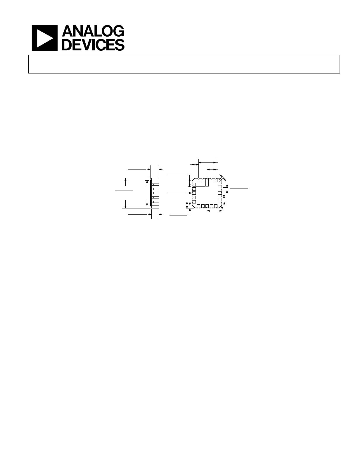
1.2.3 Case Outline.
LCC (E-20A) Package
20
1
VIEW
0.150 (3.81)
BSC
0.200 (5.08)
REF
0.100 (2.54) REF
0.015 (0.38)
MIN
3
4
0.028 (0.71)
0.022 (0.56)
0.050 (1.27)
8
BSC
9
45° TYP
0.100 (2.54)
0.064 (1.63)
0.358 (9.09)
0.342 (8.69)
SQ
0.088 (2.24)
0.054 (1.37)
0.358
(9.09)
MAX
SQ
0.075 (1.91)
0.095 (2.41)
0.075 (1.90)
0.011 (0.28)
0.007 (0.18)
R TYP
0.075 (1.91)
REF
0.055 (1.40)
0.045 (1.14)
REF
19
18
14
13
BOTTOM
CONTROLL ING DIMENS IONS ARE IN INCHES; MILLIMETER DIMENSIONS
(IN PARENTHESES) ARE ROUNDED-OF F INCH EQUI VALENTS FOR
REFERENCE ONLY AND ARE NOT APPROPRI ATE FOR USE IN DESIGN.
022106-A
(X) Package Description
E E-20A 20-Terminal Leadless Chip Carrier
1.3 Absolute Maximum Ratings (T
= +25°C, unless otherwise noted).
A
Supply Voltage ....................................................................................................................................................................................................... ±18 V
Internal Power Dissipation
1
............................................................................................................................................................................ 650 mW
Input Voltage ............................................................................................................................................................................................................. ±V
Differential Input Voltage
2
................................................................................................................................................................................. ±0.7 V
Output Short-Circuit Duration ..................................................................................................................................................................... Indefinite
Storage Temperature Range .............................................................................................................................................................. –65°C to +150°C
Operating Temperature Range ......................................................................................................................................................... –55°C to +125°C
Lead Temperature Range (Soldering 60 sec) ..................................................................................................................................................... 300°C
1
Maximum package power dissipation vs. ambient temperature.
MAXIMUM AMBIENT DERATE ABOVE MAXIMUM
Package Type Temperature for Rating Ambient Temperature
LCC (E-20A) 90°C 5.7 mW/°C
2
The input pins of this amplifier are protected by back-to-back diodes. If the differential voltage exceeds ±0.7 V, external series protection resistors should be added to
limit the input current to less than 25 mA.
1.4 Thermal Characteristics.
Thermal Resistance: θ
θ
= 25°C/W for E-20A Package
JC
= 95°C/W for E-20A Package
JC
S
Rev. C
Information furnished by Analog Devices is believed to be accurate and reliable. However, no
responsibility is assumed by Analog Devices for its use, nor for any infringements of patents or other
rights of third parties that may result from its use. Specifications subject to change without notice. No
license is granted by implication or otherwise under any patent or patent rights of Analog Devices.
Trademarks and registered trademarks are the property of their respective owners.
One Technology Way, P.O. Box 9106, Norwood, MA 02062-9106, U.S.A.
Tel: 781.329.4700 www.analog.com
Fax: 781.461.3113 ©1994–2007 Analog Devices, Inc. All rights reserved.
AD704/883B
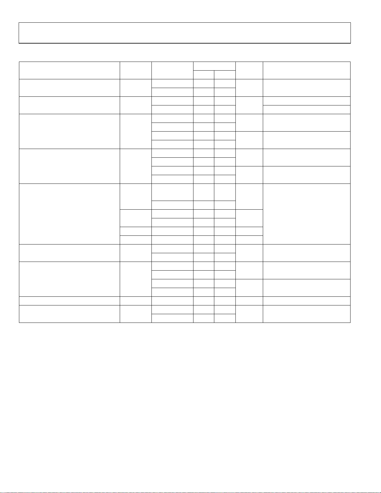
Table 1.
Limits
Test Symbol Sub Group Min Max Unit Test Conditions
Input Offset Voltage VOS 1 150 μV
2, 3 250
Power Supply Rejection Ratio PSRR 1 100 dB ±2 V ≤ VS ≤ ±18 V
2, 3 100 ±2.5 V ≤ VS ≤ ±18 V
Input Bias Current
2
IB 1 270 pA Either input, VCM = 0 V
2, 3 600
1 300 pA Either input, VCM = ±13.5 V
2, 3 700
Input Offset Current IOS 1 250 pA VCM = 0 V
2, 3 400
1 300 pA VCM = ±13.5 V
2, 3 500
Matching Characteristics
Offset Voltage VOS 1 250 μV
2, 3 400
Input Bias Current
3
I
1 500 pA
B
2, 3 600
Common-Mode Rejection4 CMR 1, 2, 3 94 dB
Power Supply Rejection
5
PSR 1, 2, 3 94 dB
Common-Mode Rejection Ratio CMRR 1 100 dB VCM = ±13.5 V
2, 3 98
Open-Loop Gain AOL 1 200 V/mV VO = ±12 V, RL = 10 kΩ
2, 3 150
1 200 V/mV VO = ±10 V, RL = 2 kΩ
2, 3 100
Output Voltage Swing V
1, 2, 3 ±13 V RL = 10 kΩ
OUT
Power Supply Quiescent Current IQ 1 2.5 mA
2, 3 2.8
1
VS = ±15 V, unless otherwise noted.
2
Bias current specifications maximum at either input.
3
Input bias current match is the maximum difference between the corresponding inputs of all four amplifiers.
4
CMR match is the difference between ΔVOS/ΔVCM for any two amplifiers, expressed in dB.
5
PSR match is the difference between ΔVOS/ΔV
for any two amplifiers, expressed in dB.
SUPPLY
1
Rev. C | Page 2 of 3

AD704/883B
+
+
3.2.1 Functional Block Diagram and Terminal Assignments.
LCC (E-20A) Connection Diagram
AD704
11NC10
1NC2
AMP 4
AMP 3
12
OUT3
–IN420OUT4
19
18
+IN4
17
NC
16
–V
S
15
NC
14
+IN3
13
–IN3
7006-001
OUT13–IN1
4
IN1
5
NC
AMP 1
6
+V
S
AMP 2
7
NC
8
IN2
9
–IN2
NC = NO CONNECT
OUT2
3.2.4 Microcircuit Technology Group.
This microcircuit is covered by technology group (49).
4.2.1
Life Test/Burn-In Circuit.
Steady state life test is per MIL-STD-883 Method 1005. Burn-in MIL-STD-833 Method 1015 Test Condition (B).
+10V
2kΩ
2kΩ
3
4
8
9
MR-820
2kΩ
+15V
1
2
16
–15V
2kΩ
0.1µF
6
2
2kΩ
2kΩ
10
0.1µF
MR-820
2kΩ
19
4
18
LCC PIN
DESIGNATORS
SHOWN
14
3
13
2kΩ
20
12
MR-820
+15V +10V
©1994–2007 Analog Devices, Inc. All rights reserved. Trademarks and
registered trademarks are the property of their respective owners.
C07006-0-8/07(C)
47µF
+
47µF
+
–15V
47µF
+
07006-002
Rev. C | Page 3 of 3
 Loading...