

AD6650 Diversity IF-to-Baseband
K
www.BDTIC.com/ADI
FEATURES
116 dB dynamic range
Digital VGA
I/Q demodulators
Active low-pass filters
Dual wideband ADC
Programmable decimation and channel filters
VCO and phase-locked loop circuitry
Serial data output ports
Intermediate frequencies of 70 MHz to 260 MHz
10 dB noise figure
+43 dBm input IP2 at 70 MHz IF
−9.5 dBm input IP3 at 70 MHz IF
3.3 V I/O and CMOS core
Microprocessor interface
JTAG boundary scan
APPLICATIONS
PHS or GSM/EDGE single carrier, diversity receivers
Microcell and picocell systems
Wireless local loop
GSM/EDGE Narrow-Band Receiver
AD6650
Smart antenna systems
Software radios
In-building wireless telephony
PRODUCT DESCRIPTION
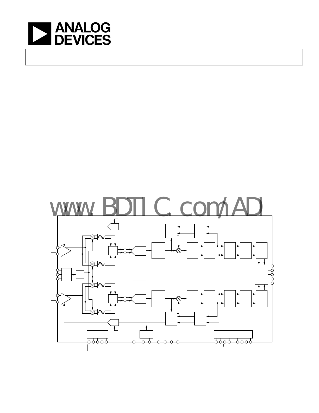
The AD6650 is a diversity intermediate frequency-to-baseband
(IF-to-baseband) receiver for GSM/EDGE. This narrow-band
receiver consists of an integrated DVGA, IF-to-baseband I/Q
demodulators, low-pass filtering, and a dual wideband ADC.
The chip can accommodate IF input from 70 MHz to 260 MHz.
The receiver architecture is designed such that only one external
surface acoustic wave (SAW) filter for main and one for diversity
are required in the entire receive signal path to meet GSM/EDGE
blocking requirements.
Digital decimation and filtering circuitry provided on-chip
remove unwanted signals and noise outside the channel of
interest. Programmable RAM coefficient filters allow antialiasing,
matched filtering, and static equalization functions to be combined
in a single cost-effective filter. The output of the channel filters
is provided to the user via serial output I/Q data streams.
AIN
AIN
CPOUT
VLDO
BIN
BIN
FUNCTIONAL BLOCK DIAGRAM
TWEAK GAIN
DAC
I
LPF
12-BIT
REF/4
12-BIT
SYNC
LPF
LPF
LPF
TDI
MUX
Q
Q
MUX
I
DAC
TWEAK GAIN
TDO
TMS
VGA
PLL/
LF
VCO
VGA
0
90
JTAG
TRST
TCLK
ADC
ADC
CLK
DIVIDER
CLK
COARSE
COARSE
CLK
DCC
DCC
AGC
RELIN
CTRL
AGC
RELIN
CTRL
DVDD
AVDD
DGND
AGND
TH
4
ORDER
CIC
TH
4
ORDER
CIC
LP
FILTER
LP
FILTER
TH
7
ORDER
IIR
TH
7
ORDER
IIR
RESET
Figure 1.
AD6650 GSM/
EDGE IF RECEIVER
CS
PROG.
(RCF)
PROG.
(RCF)
R/W
FIR
FIR
MICRO
DS
FINE
DCC
FINE
DCC
A[2:0]
MODE [2:0]
BIST
SCL
SERIAL
PORT
BIST
D[7:0]
DTACK
SDFS
SDO0
SDO1
DR
03683-001
Rev. A
Information furnished by Analog Devices is believed to be accurate and reliable. However, no
responsibility is assumed by Anal og Devices for its use, nor for any infringements of patents or ot her
rights of third parties that may result from its use. Specifications subject to change without notice. No
license is granted by implication or otherwise under any patent or patent rights of Analog Devices.
Trademarks and registered trademarks are the property of their respective owners.
One Technology Way, P.O. Box 9106, Norwood, MA 02062-9106, U.S.A.
Tel: 781.329.4700 www.analog.com
Fax: 781.461.3113 ©2006–2007 Analog Devices, Inc. All rights reserved.

AD6650
www.BDTIC.com/ADI
TABLE OF CONTENTS
Features.............................................................................................. 1
Applications....................................................................................... 1
Product Description......................................................................... 1
Functional Block Diagram .............................................................. 1
Revision History ............................................................................... 2
Specifications..................................................................................... 3
Explanation of Test Levels........................................................... 3
AC Specifications.......................................................................... 3
Digital Specifications ................................................................... 4
Electrical Characteristics ............................................................. 5
General Timing Characteristics ................................................. 5
Microprocessor Port Timing Characteristics ........................... 6
Timing Diagrams.......................................................................... 7
Absolute Maximum Ratings.......................................................... 10
Thermal Characteristics ............................................................10
ESD Caution................................................................................ 10
Pin Configuration and Function Descriptions........................... 11
Typical Performance Characteristics ........................................... 13
Terminology .................................................................................... 14
Equivalent Circuits......................................................................... 15
Theory of Operation ...................................................................... 16
Analog Front End....................................................................... 16
Digital Back End......................................................................... 16
DC Correction ............................................................................16
Fourth-Order Cascaded Integrator Comb Filter (CIC4)...... 17
Infinite Impulse Response (IIR) Filter..................................... 18
RAM Coefficient Filter .............................................................. 18
Composite Filter......................................................................... 19
Fine DC Correction ................................................................... 20
Peak Detector DC Correction Ranging................................... 20
User-Configurable Built-In Self-Test (BIST).......................... 21
LO Synthesis................................................................................ 22
LDO.............................................................................................. 23
AGC Loop/Relinearization....................................................... 23
Serial Output Data Port............................................................. 24
Application Information................................................................ 26
Required Settings and Start-up Sequence for DC Correction
....................................................................................................... 26
Clocking the AD6650 ................................................................ 26
Driving the Analog Inputs........................................................ 27
External Reference ..................................................................... 27
Power Supplies............................................................................ 27
Digital Outputs........................................................................... 28
Grounding................................................................................... 28
Layout Information.................................................................... 28
Chip Synchronization................................................................ 29
Microport Control.......................................................................... 30
External Memory Map .............................................................. 30
Access Control Register (ACR) ................................................ 30
Channel Address Register (CAR) ............................................ 30
Special Function Registers ........................................................ 30
Data Address Registers.............................................................. 31
Write Sequencing ....................................................................... 31
Read Sequencing ........................................................................ 31
Read/Write Chaining................................................................. 31
Programming Modes................................................................. 31
JTAG Boundary Scan................................................................. 32
Register Map ................................................................................... 33
Register Details........................................................................... 39
Outline Dimensions....................................................................... 44
Ordering Guide .......................................................................... 44
REVISION HISTORY
1/07—Rev. 0 to Rev. A
Updated Format..................................................................Universal
Changes to Specifications................................................................ 3
Changes to Figure 18...................................................................... 13
Changes to Power Supplies Section.............................................. 27
Changes to Ordering Guide.......................................................... 44
3/06—Revision 0: Initial Version
Rev. A | Page 2 of 44

AD6650
www.BDTIC.com/ADI
SPECIFICATIONS
EXPLANATION OF TEST LEVELS
I. 100% production tested.
II. 100% p
III. S
IV. P
V. P
VI. 100% p
VII. 100% p
C
= 40 pF on all outputs, unless otherwise specified. All timing specifications valid over VDD range of 3.0 V to 3.45 V and VDDIO
LOAD
range of 3.0 V to 3.45 V.
AC SPECIFICATIONS
AVDD and DVDD = 3.3 V, CLK = 52 MSPS (driven differentially), 50% duty cycle, unless otherwise noted. All minimum ac
specifications are guaranteed from −25°C to +85°C. AC minimum specifications degrade slightly from −25°C to −40°C.
Table 1.
Parameter Temp Test Level Min Typ Max Unit
OVERALL FUNCTION
Frequency Range Full V 70 260 MHz
GAIN CONTROL
Gain Step Size 25°C V 0.094 dB
Gain Step Accuracy 25°C V ±0.047 dB
AGC Range 25°C V 36 dB
BASEBAND FILTERS
Bandwidth Full IV 3.36 3.5 3.64 MHz
Alias Rejection at 25.9 MHz 25°C V 77 dB
LO PHASE NOISE
At 10 kHz Offset 25°C V −79 dBc/Hz
At 20 kHz Offset 25°C V −87 dBc/Hz
At 50 kHz Offset 25°C V −103 dBc/Hz
At 100 kHz Offset 25°C V −112 dBc/Hz
At 200 kHz Offset 25°C V −119 dBc/Hz
At 400 kHz Offset 25°C V −125 dBc/Hz
At 600 kHz Offset 25°C V −130 dBc/Hz
At 800 kHz Offset 25°C V −133 dBc/Hz
At 1600 kHz Offset 25°C V −138 dBc/Hz
At 3000 kHz Offset 25°C V −143 dBc/Hz
GAIN ERROR 25°C V −0.7 dB
PSRR (AVDD with 20 mV RMS Ripple)
At 5 kHz 25°C V −13.4 dBc
At 10 kHz 25°C V −17 dBc
At 50 kHz 25°C V −34 dBc
At 100 kHz 25°C V −39.8 dBc
At 150 kHz 25°C V −45.7 dBc
f = 70 MHz
Coarse DC Correction V −70 dB
Noise Figure2 V 10 dB
Input IP2
Input IP3
Image Rejection Full IV −49 −33 dBc
Full-Scale Input Power V 4 dBm
Input Impedance V 189.6 − j33.6 Ω
roduction tested at 25°C; sample tested at specified temperatures.
ample tested only.
arameter guaranteed by design and analysis.
arameter is typical value only.
roduction tested at 25°C; sample tested at temperature extreme.
roduction tested at +85°C.
1
2
2
Full IV 24 43 dBm
Full IV −15 −9.5 dBm
Rev. A | Page 3 of 44

AD6650
www.BDTIC.com/ADI
Parameter Temp Test Level Min Typ Max Unit
f = 150 MHz
Coarse DC Correction V −70 dB
Noise Figure2 V 10 dB
Input IP22 Full IV 24 37 dBm
Input IP32 Full IV −15 −11.5 dBm
Image Rejection Full IV −46.5 −33 dBc
Full-Scale Input Power V 4 dBm
Input Impedance V 169.3 − j59.2 Ω
f = 200 MHz
Coarse DC Correction V −70 dB
Noise Figure2 V 10 dB
Input IP22 Full IV 24 35 dBm
Input IP32 Full IV −16 −12 dBm
Image Rejection Full IV −46.5 −33 dBc
Full-Scale Input Power V 4 dBm
Input Impedance V 159.3 − j66.9 Ω
f = 250 MHz
Coarse DC Correction V −70 dB
Noise Figure2 V 10 dB
Input IP22 Full VII 24 33 dBm
Input IP32 Full VII −16 −13 dBm
Image Rejection Full VII −45 −33 dBc
Full-Scale Input Power V 4 dBm
Input Impedance V 137.1 − j72.7 Ω
1
See Figure 40 and Figure 41 for additional PSRR specifications.
2
This measurement applies for maximum gain (36 dB).
DIGITAL SPECIFICATIONS
AVDD and DVDD = 3.3 V, CLK = 52 MSPS, unless otherwise noted.
Table 2.
Parameter Temp Test Level Min Typ Max Unit
DVDD Full IV 3.0 3.3 3.45 V
AVDD Full IV 3.0 3.3 3.45 V
1
T
IV −25 +25 +85 °C
AMBIENT
1
The AD6650 is guaranteed fully functional from −40°C to +85°C. All ac minimum specifications are guaranteed from −25°C to +85°C, but degrade slightly from −25°C
to −40°C.
Rev. A | Page 4 of 44

AD6650
www.BDTIC.com/ADI
ELECTRICAL CHARACTERISTICS
Table 3.
Parameter (Conditions) Temp Test Level Min Typ Max Unit
LOGIC INPUTS
Logic Compatibility Full IV 3.3 V CMOS
Digital Logic
Logic 1 Voltage Full IV 2.0 VDD V
Logic 0 Voltage Full IV 0 0.8 V
Logic 1 Current 25°C V 60 μA
Logic 0 Current 25°C V 7 μA
Input Capacitance 25°C V 5 pF
CLOCK INPUTS
Differential Input Voltage
Common-Mode Input Voltage 25°C V DVDD/2 V
Differential Input Resistance 25°C V 7.5 kΩ
Differential Input Capacitance 25°C V 5 pF
LOGIC OUTPUTS
Logic Compatibility Full 3.3 V CMOS/TTL
Logic 1 Voltage (IOH = 0.25 mA) Full IV 2.4 VDD − 0.2 V
Logic 0 Voltage (IOL = 0.25 mA) Full IV 0.2 0.8 V
IDD SUPPLY CURRENT
CLK = 52 MHz (GSM Example)
I
Full VII 155 mA
DVDD
I
Full VII 360 mA
AVDD
POWER DISSIPATION
CLK = 52 MHz (GSM/EDGE Example) Full VII 1.7 2.1 W
1
All ac specifications are tested by driving CLK and
GENERAL TIMING CHARACTERISTICS
Table 4.
Parameter (Conditions) Symbol Temp Test Level Min Typ Max Unit
CLK TIMING REQUIREMENTS
CLK Period
CLK Width Low t
CLK Width High t
RESET TIMING REQUIREMENTS
RESET Width Low
PIN_SYNC TIMING REQUIREMENTS
SYNC to ↑ CLK Setup Time
SYNC to ↑ CLK Hold Time
SERIAL PORT TIMING REQUIREMENTS: SWITCHING CHARACTERISTICS
↑ CLK to ↑ SCLK Delay (Divide-by-1)
↑ CLK to ↑ SCLK Delay (For Any Other Divisor)
↑ CLK to ↓ SCLK Delay (Divide-by-2 or Even Number)
↓ CLK to ↓ SCLK Delay (Divide-by-3 or Odd Number)
↑ SCLK to SDFS Delay
↑ SCLK to SDO0 Delay
↑ SCLK to SDO1 Delay
↑ SCLK to DR Delay
1
Minimum specification is based on a 104 MSPS clock rate (an internal divide-by-2 must be used with a 104 MSPS clock rate); maximum specification is based on a
52 MSPS clock rate. This device is optimized to operate at a clock rate of 52 MSPS or 104 MSPS.
2
The timing parameters for SCLK, SDFS, SDO0, SDO1, and DR apply to both Channel 0 and Channel 1.
1
1
CLK
differentially.
25°C V 0.4 3.6 V p-p
t
Full I 9.6 19.2 ns
CLK
Full IV 0.5 × t
CLKL
Full IV 0.5 × t
CLKH
ns
CLK
ns
CLK
t
Full IV 30 ns
SSF
Full IV −3 ns
t
SS
tHS Full IV 6 ns
2
t
Full IV 3.2 12.5 ns
DSCLK1
t
Full IV 4.4 16 ns
DSCLKH
t
Full IV 4.7 16 ns
DSCLKL
Full IV 4 14 ns
t
DSCLKLL
Full IV 1 2.6 ns
t
DSDFS
Full IV 0.5 3.5 ns
t
DSDO0
t
Full IV 0.5 3.5 ns
DSDO1
t
Full IV 1 3.5 ns
DSDR
Rev. A | Page 5 of 44
AD6650
www.BDTIC.com/ADI
MICROPROCESSOR PORT TIMING CHARACTERISTICS
All timing specifications valid over VDD range of 3.0 V to 3.45 V and VDDIO range of 3.0 V to 3.45 V.
Table 5. Microprocessor Port, Mode INM (MODE = 0); Asynchronous Operation
Parameter Symbol Temp Test Level Min Typ Max Unit
WRITE TIMING
WR (R/W) to RDY (DTACK) Hold Time
Address/Data to WR (R/W) Setup Time
Address/Data to RDY (DTACK) Hold Time
WR (R/W) to RDY (DTACK) Delay
WR (R/W) to RDY (DTACK) High Delay
READ TIMING
Address to RD (DS) Setup Time
Address to Data Hold Time
Data Three-state Delay
RDY (DTACK) to Data Delay
1
1
1
RD (DS) to RDY (DTACK) Delay
RD (DS) to RDY (DTACK) High Delay
1
Timing is guaranteed by design.
2
Specification pertains to control signals R/W, WR, DS, RD, and CS such that the minimum specification is valid after the last control signal has reached a valid logic level.
1
1
1
1
1
t
Full IV 0.0 ns
HWR
t
Full IV 0.0 ns
SAM
t
Full IV 0.0 ns
HAM
2
t
t
t
t
DRDY
ACC
SAM
HAM
Full IV 9.0 15.0 ns
Full IV 4 × t
13 × t
CLK
ns
CLK
Full IV 0.0 ns
Full IV 0.0 ns
tZD Full V 12 ns
tDD Full IV 0.0 ns
2
t
1
t
DRDY
ACC
Full IV 9.0 15.0 ns
Full IV 4 × t
13 × t
CLK
CLK
ns
Table 6. Microprocessor Port, Mode MNM (MODE = 1)
Parameter Symbol Temp Test Level Min Typ Max Unit
WRITE TIMING
t
DS (RD) to DTACK (RDY) Hold Time
R/W (WR) to DTACK (RDY) Hold Time
Address/Data to R/W (WR) Setup Time
Address/Data to R/W (WR) Hold Time
DS (RD) to DTACK (RDY) Delay
2
R/W (WR) to DTACK (RDY) Low Delay
1
1
1
Full IV 15.0 ns
HDS
t
Full IV 15.0 ns
HRW
t
Full IV 0.0 ns
SAM
t
Full IV 0.0 ns
HAM
t
Full V 16 ns
DDTACK
t
Full IV 4 × t
ACC
13 × t
CLK
ns
CLK
READ TIMING
t
DS (RD) to DTACK (RDY) Hold Time
Address to DS (RD) Setup Time
Address to Data Hold Time
1
1
Full IV 15.0 ns
HDS
t
Full IV 0.0 ns
SAM
t
Full IV 0.0 ns
HAM
Data Three-State Delay tZD Full V 13 ns
DTACK (RDY) to Data Delay
DS (RD) to DTACK (RDY) Delay
DS (RD) to DTACK (RDY) Low Delay
1
Timing is guaranteed by design.
2
DTACK
is an open-drain device and must be pulled up with a 1 kΩ resistor.
1
2
1
tDD Full IV 0.0 ns
t
Full V 16 ns
DDTACK
t
Full IV 4 × t
ACC
13 × t
CLK
ns
CLK
Rev. A | Page 6 of 44
AD6650
SCLK
S
S
S
S
S
www.BDTIC.com/ADI
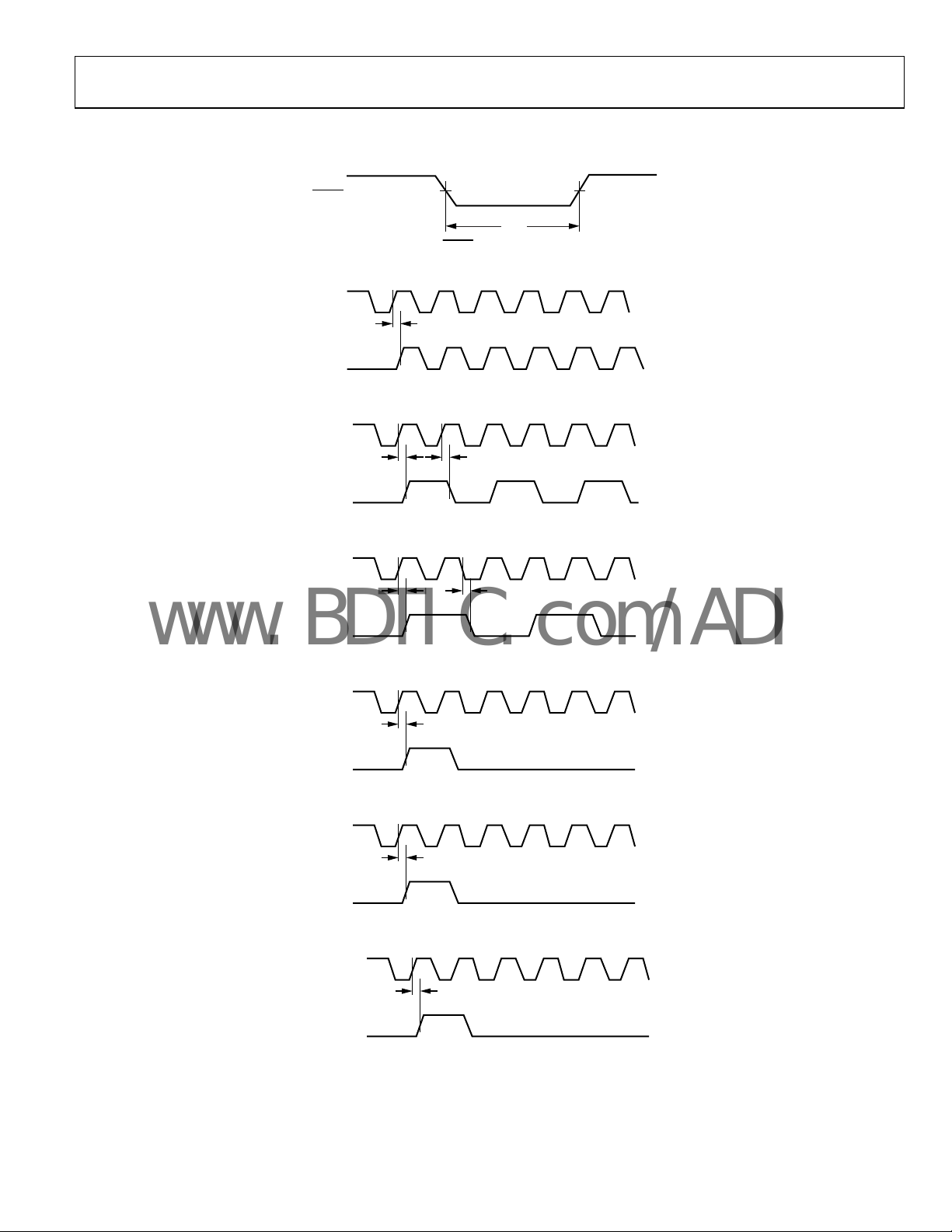
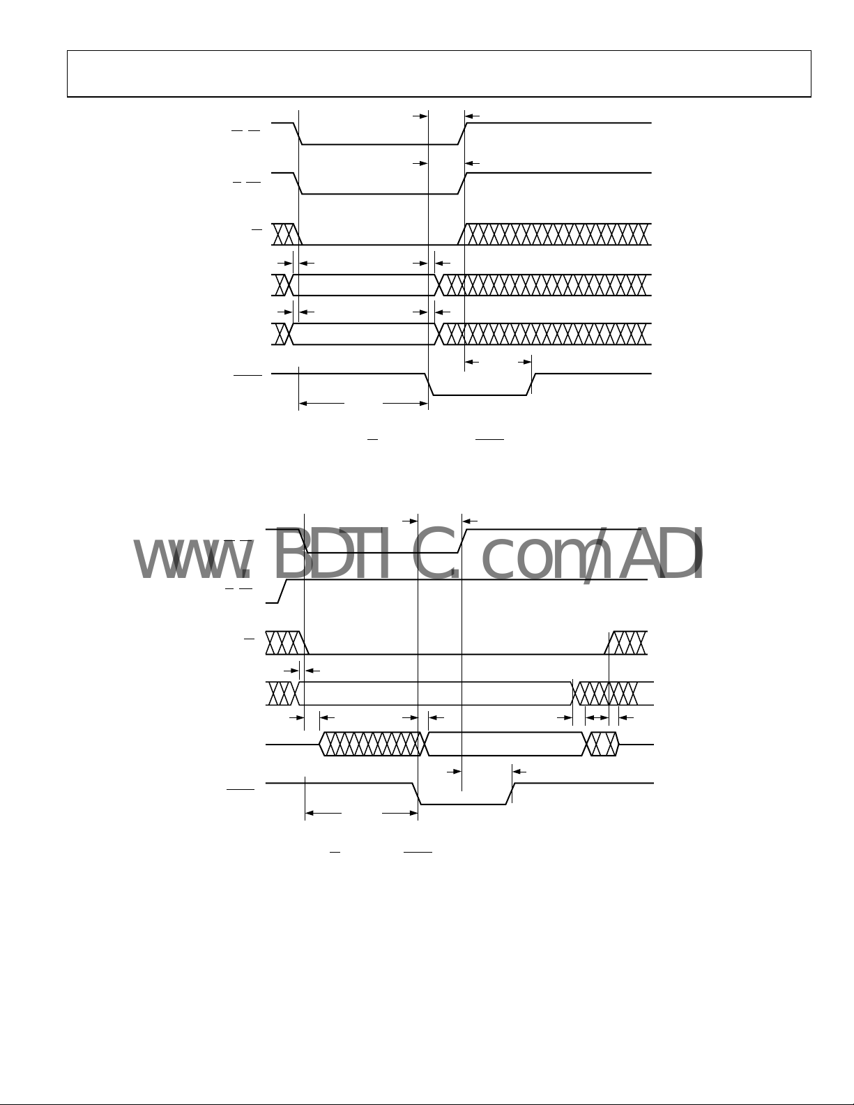
TIMING DIAGRAMS
RESET
t
SSF
RESET
Figure 2.
Timing Requirements
CLK
t
DSCLKH
Figure 3. SCLK Switching Characteristics (Divide-by-1)
CLK
t
DSCLKH
t
DSCLKL
03683-002
03683-003
CLK
03683-004
Figure 4. SCLK Switching Characteristics (Divide-by-2 or Even Integer)
CLK
CLK
t
DSCLKH
t
DSCLKL L
03683-005
Figure 5. SCLK Switching Characteristics (Divide-by-3 or Odd Integer)
CLK
t
DSDR
DR
03683-006
Figure 6. SCLK, DR Switching Characteristics
CLK
t
DSDFS
SDFS
03683-007
Figure 7. SCLK, SDFS Switching Characteristics
SCLK
t
DSD0/tDSD1
DO0/SDO1
Figure 8. SCLK, SDO0/SDO1 Switching Characteristics
Rev. A | Page 7 of 44
03683-008
AD6650
W
W
www.BDTIC.com/ADI
CLK
t
HS
03683-009
SYNC
t
SS
Figure 9. SYNC Timing Inputs
RD (DS)
t
HWR
R (R/W)
CS
t
t
HAM
HAM
03683-010
A[2:0]
D[7:0]
RDY
(DTACK)
t
SAM
VALID ADDRESS
t
SAM
VALID DATA
t
DRDY
t
ACC
NOTES
1.
t
ACCESS TIME DEPENDS ON THE ADDRESS ACCESS ED. ACCESS TI ME IS MEASURED
ACC
FROM FALLING EDGE OF WRTO RISING EDGE OF RDY.
2.
t
REQUIRES A MAXIMUM OF NINE CLK PERI ODS.
ACC
Figure 10. INM Microport Write Timing Requirements
RD (DS)
R (R/W)
CS
t
SAM
t
ACC
VALID ADDRESS
A[2:0]
t
ZD
D[7:0]
t
DRDY
RDY
(DTACK)
NOTES
1.
t
ACCESS TIME DE PENDS ON THE ADDRESS ACCESSED. ACCESS TI ME IS MEASURED
ACC
FROM FALLING EDGE OF RD TO RISING EDGE OF RDY.
2.
t
REQUIRES A MAXIMUM OF 13 CLK PERIODS.
ACC
Figure 11. INM Microport Read Timing Requirements
t
DD
Rev. A | Page 8 of 44
VALID DATA
t
HAM
t
ZD
03683-011
AD6650
www.BDTIC.com/ADI
t
HDS
DS (RD)
t
HRW
R/W (W R)
CS
t
ACC
t
t
HAM
HAM
t
DDTACK
03683-012
t
SAM
A[2:0]
D[7:0]
DTACK
(RDY)
NOTES
1.
t
ACCESS TIME DEPENDS ON THE ADDRESS ACCESSE D. ACCESS TIM E IS MEASURED
ACC
FROM FALLING EDG E OF DS TO FALLING EDGE OF DTACK.
2.
t
REQUIRES A MAXIMUM OF NINE CLK PERI ODS.
ACC
VALID ADDRESS
t
SAM
VALID DATA
Figure 12. MNM Microport Write Timing Requirements
t
HDS
DS (RD)
R/W (WR)
CS
t
SAM
A[2:0]
D[7:0]
DTACK
(RDY)
t
ZD
t
ACC
NOTES
1.
t
ACCESS TIME DEPENDS ON THE ADDRESS ACCESS ED. ACCESS TI ME IS MEASURED
ACC
FROM FALLING EDGE OF DSTO THE FALLING EDGE OF DTACK.
2.
t
REQUIRES A MAXIMUM O F 13 CLK PERIODS.
ACC
VALID ADDRESS
t
DD
t
DDTACK
VALID DATA
t
HAM
t
ZD
03683-013
Figure 13. MNM Microport Read Timing Requirements
Rev. A | Page 9 of 44
AD6650
www.BDTIC.com/ADI
ABSOLUTE MAXIMUM RATINGS
Table 7.
Parameter Rating
Supply Voltage −0.3 V to +3.6 V
Input Voltage −0.3 V to +3.6 V
Output Voltage Swing −0.3 V to VDDIO + 0.3 V
Load Capacitance 200 pF
Junction Temperature Under Bias 125°C
Storage Temperature Range −65°C to +150°C
Lead Temperature (5 sec) 280°C
Stresses above those listed under Absolute Maximum Ratings
may cause permanent damage to the device. This is a stress
rating only; functional operation of the device at these or any
other conditions above those indicated in the operational
section of this specification is not implied. Exposure to absolute
maximum rating conditions for extended periods may affect
device reliability.
THERMAL CHARACTERISTICS
121-lead chip scale package ball grid array:
= 22.8°C/W, no airflow, measurements made in the
θ
JA
horizontal position on a 4-layer board.
= 20.2°C/W, 200 LFPM airflow, measurements made in the
θ
JA
horizontal position on a 4-layer board.
= 20.7°C/W, no airflow, soldered on an 8-layer board with
θ
JA
two layers dedicated as ground planes.
ESD CAUTION
Rev. A | Page 10 of 44
AD6650
A
A
R
www.BDTIC.com/ADI
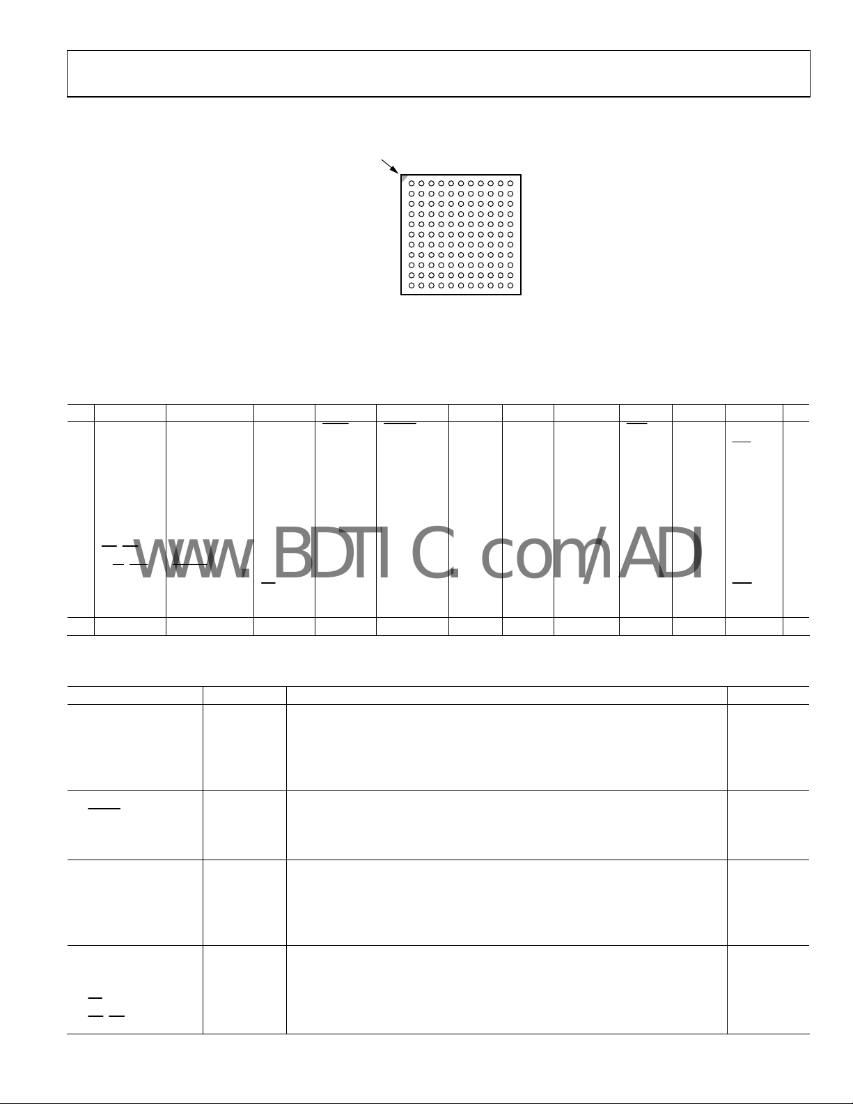
PIN CONFIGURATION AND FUNCTION DESCRIPTIONS
1 CORNE
INDEX AREA
6
3
245
1
AD6650
TOP VIEW
(Not to Scale)
Figure 14. Pin Configuration
Table 8. Pin Configuration
1 2 3 4 5 6 7 8 9 10 11
DGND TDI TMS
A
SDFS SCLK TDO TCLK SYNC DNC AVDD AVDD AGND AGND
B
SDO1 SDO0 DVDD DVDD DVDD DVDD AVDD AVDD AGND AGND BIN
C
D7 DR DVDD DGND DGND DGND AVDD AVDD AGND AGND AGND
D
D5 D6 DVDD DGND DGND DGND AVDD AVDD AGND AGND LF
E
D3 D4 DVDD DGND DGND DGND AVDD AVDD AGND DNC VLDO
F
D1 D2 DVDD DGND DGND DGND AVDD AVDD AGND AGND CPOUT
G
(RD)
DS
H
(WR) DTACK (RDY)
R/W
J
A2 A1
K
DGND A0 MODE2 MODE0 CHIP_ID0 DNC AVDD VREF REFB AGND AGND
L
1 2 3 4 5 6 7 8 9 10 11
D0 DVDD DGND DGND DGND AVDD AVDD AGND AGND AGND
DVDD DVDD DVDD DVDD AVDD AVDD AGND AGND AIN
CS
TRST
MODE1 CHIP_ID1 DNC AVDD REFGND REFT AGND
RESET
9
7
11
10
8
B
C
D
E
F
G
H
J
K
L
03683-042
DNC AVDD CLK
CLK
AGND AGND
BIN
AIN
A
B
C
D
E
F
G
H
J
K
L
Table 9. Pin Function Descriptions
Mnemonic Type Description No. of Pins
POWER SUPPLY
DVDD Power 3.3 V Digital Supply. 13
AVDD Power 3.3 V Analog Supply. 19
DGND Ground Digital Ground. 17
AGND Ground Analog Ground. 22
DIGITAL INPUTS
RESET
Input Active Low Reset Pin. 1
SYNC Input Synchronizes Digital Filters. 1
CHIP_ID[1:0] Input Chip ID. 2
SERIAL DATA PORT
SCLK Bidirectional Serial Clock. 1
SDFS Bidirectional Serial Data Frame Sync. 1
SDO[1:0] Output Serial Data Outputs. Three-stated when inactive. 2
DR Output Output Data Ready Indicator. 1
MICROPORTCONTROL
D[7:0] Bidirectional Microport Data. 8
A[2:0] Input Microport Address Bits. 3
CS
DS (RD)
Input Chip Select. 1
Input Active Low Data Strobe (Active Low Read). 1
Rev. A | Page 11 of 44

AD6650
www.BDTIC.com/ADI
Mnemonic Type Description No. of Pins
DTACK (RDY)
R/W (WR)
MODE [2:0] Input Selects Control Port Mode. 3
JTAG
TRST
TCLK Input Test Clock Input. 1
TMS Input Test Mode Select Input. 1
TDO Output Test Data Output. Three-stated when JTAG is in reset. 1
TDI Input Test Data input. 1
ANALOG INPUTS
AIN Input Main Analog Input. 1
AIN
BIN Input Diversity Analog Input. 1
BIN
PLL INPUTS
CPOUT Output Charge-Pump Output. 1
LF Input Loop Filter. 1
VLDO Output
REFT Output
REFB Output
VREF Output
REFGND Ground ADC Ground Reference. See Figure 39 for recommended connection. 1
CLOCK INPUTS
CLK Input Encode Input. Conversion initiated on rising edge. 1
CLK
DNC Do Not Connect. 5
Output
Input Read Write (Active Low Write). 1
Input Test Reset Pin. 1
Input Complement of AIN. Differential analog input. 1
Input Complement of BIN. Differential analog input. 1
Input Complement of Encode. 1
Active Low Data Acknowledge (Microport Status Bit). Open-drain output, requires
external pull-up resistor of 1 kΩ.
Compensation for Internal Low Dropout Regulator. Bypass to ground with a 220
nF chip ca
Internal ADC Voltage Reference. Bypass to ground with capacitors. See Figure 39
or recommended connection.
f
Internal ADC Voltage Reference. Bypass to ground with capacitors. See Figure 39
or recommended connection.
f
Internal ADC Voltage Reference. Bypass to ground with capacitors. See Figure 39
or recommended connection.
f
pacitor.
1
1
1
1
1
Rev. A | Page 12 of 44
AD6650
–
–
www.BDTIC.com/ADI
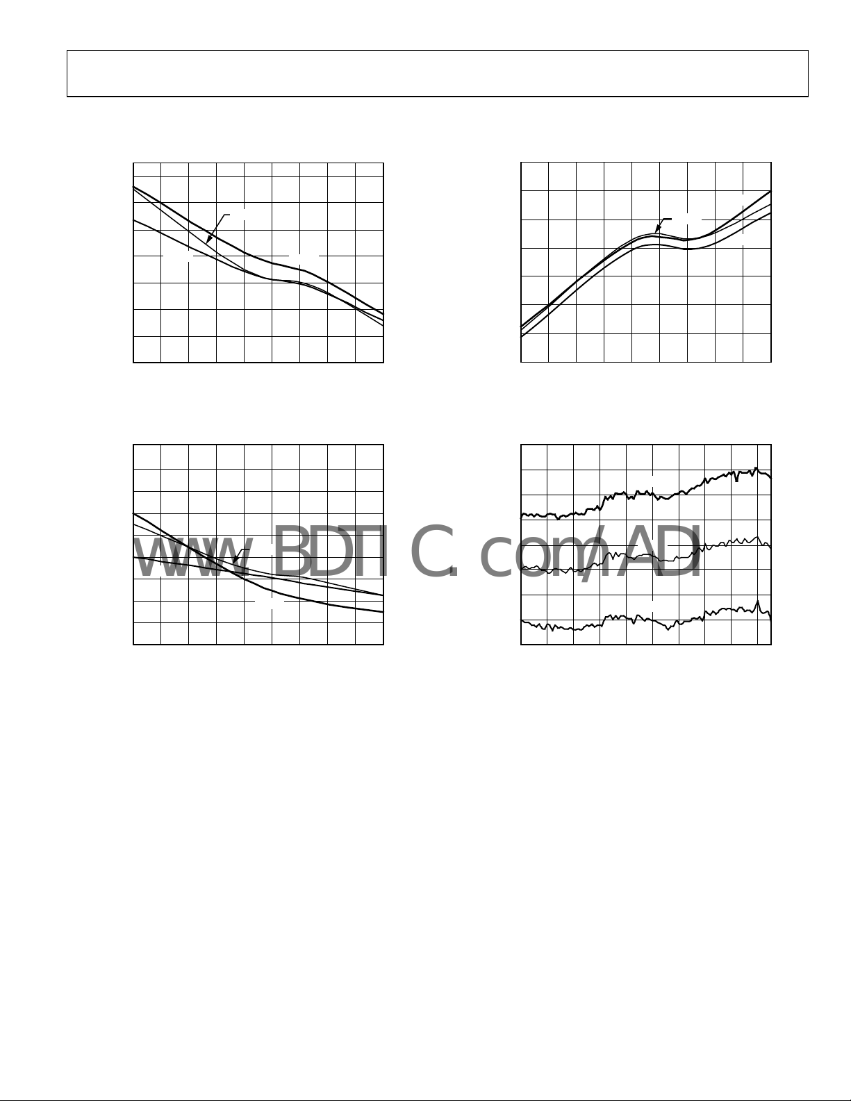
TYPICAL PERFORMANCE CHARACTERISTICS
44
42
40
38
IIP2 (dBm)
36
34
32
30
–25°C
70 90 110 130 150 170 190 210 230 250
+25°C
+85°C
IF FREQUENCY ( MHz)
Figure 15. Input IP2 vs. Frequency
6
–7
–8
–9
–10
–11
IIP3 (dBm)
–25°C
–12
–13
–14
–15
70 90 110 130 150 170 190 210 230 250
+25°C
+85°C
IF FREQUENCY ( MHz)
Figure 16. Input IP3 vs. Frequency
44
–45
–46
–47
–48
IMAGE (d Bc)
–49
–50
03683-016
–51
70 90 110 130 150 170 190 210 230 250
IF FREQUENCY ( MHz)
+25°C
–25°C
+85°C
03683-018
Figure 17. Image vs. Frequency
0.2
0
–0.2
–0.4
–0.6
–0.8
GAIN ERROR (dB)
–1.0
–1.2
03683-017
–1.4
70 90 110 130 150 170 190 210 230 250
–25°C
+25°C
+85°C
IF FREQUENCY ( MHz)
03683-019
Figure 18. Gain Error vs. Frequency
Rev. A | Page 13 of 44

AD6650
www.BDTIC.com/ADI
TERMINOLOGY
Analog Bandwidth
The analog input frequency at which the spectral power of the
f
undamental frequency (as determined by the FFT analysis) is
reduced by 3 dB.
Noise Figure (NF)
The degradation in SNR performance (in dB) of an IF input
sig
nal after it passes through a component or system.
The AD6650 noise figure is determined by the equation
NF
⎛
⎜
=
⎜
⎝
2
⎛
rms
⎜
log10
⎜
⎝
⎞
ZV
in
⎟
−
⎟
001.0
⎠
SNR
⎞
⎟
−
FS
⎟
⎠
kTB
⎞
⎛
log10
⎜
⎝
(1)
⎟
001.0
⎠
where:
−23
k is the B
oltzmann constant = 1.38 × 10
.
T is the temperature in kelvin.
B is the channel bandwidth in hertz (200 kHz typical).
2
V
is the full-scale input voltage.
rms
Z
is the input impedance.
in
is the computed signal-to-noise ratio referred to full scale
SNR
FS
with a small input signal and the AD6650 in maximum gain.
Input Second-Order Intercept (IIP2)
A figure of merit used to determine a component’s or system’s
su
sceptibility to intermodulation distortion (IMD) from its
second-order nonlinearities. Two unmodulated carriers at a
specified frequency relationship (f1 and f2) are injected into a
nonlinear system exhibiting second-order nonlinearities
producing IMD components at f1 − f2 and f2 − f1. IIP2
graphically represents the extrapolated intersection of the
carrier’s input power with the second-order IMD component
when plotted in decibels.
Input Third-Order Intercept (IIP3)
A figure of merit used to determine a component’s or system’s
su
sceptibility to intermodulation distortion (IMD) from its
third-order nonlinearities. Two unmodulated carriers at a
specified frequency relationship (f1 and f2) are injected into a
nonlinear system exhibiting third-order nonlinearities
producing IMD components at (2 × f1) – f2 and (2 × f2) – f1.
IIP3 graphically represents the extrapolated intersection of the
carrier’s input power with the third-order IMD component
when plotted in decibels.
Image
The AD6650 incorporates a quadrature demodulator that mixes
t
he IF frequency to a baseband frequency. The phase and amplitude
imbalance of this quadrature demodulator is observed in a complex
FFT as an image of the fundamental frequency. The term image
arises from the mirror-like symmetry of signal and image
frequencies about the beating-oscillator frequency (in this
case, this is dc).
Differential Analog Input Resistance, Differential Analog
Capacitance, and Differential Analog Input Impedance
Input
The real and complex impedances measured at each analog
put port. The resistance is measured statically, and the
in
capacitance and differential input impedances are measured
with a network analyzer.
Differential Analog Input Voltage Range
The peak-to-peak differential voltage that must be applied to
t
he converter to generate a full-scale response. Peak differential
voltage is computed by observing the voltage on a single pin
and subtracting the voltage from the other pin, which is 180°
out of phase. The peak-to-peak differential voltage is computed
by rotating the phases of the inputs 180° and taking the peak
measurement again. Then the difference is computed between
both peak measurements.
Full-Scale Input Power
Expressed in dBm. It is computed using the following equation:
Power
where Z
⎛
⎜
=
scaleFull
⎜
log10
⎜
⎜
⎜
⎝
is the input impedance.
Input
2
V
Z
scaleFull
Input
001.0
⎞
rms
⎟
⎟
(2)
⎟
⎟
⎟
⎠
Noise
The noise, including both thermal and quantization noise, for
a
ny range within the ADC is computed as
−−
SignalSNRFS
⎛
⎜
⎜
⎝
××=
ZV (3)
noise
10001.0
10
⎞
dBFSdBcdBm
⎟
⎟
⎠
where:
Z is t
he input impedance.
is the full scale of the device for the frequency in question.
FS
dBm
SNR
is the value for the particular input level.
dBc
Signal
is the signal level within the ADC reported in decibels
dBFS
below full scale.
Rev. A | Page 14 of 44

AD6650
A
V
www.BDTIC.com/ADI
EQUIVALENT CIRCUITS
AIN/BIN
1nH
CLAMP 1pF
2pF
25
75
1.3V
75
25
03683-014
AIN/BIN
1nH
Figure 19. Analog Input
DD
20k 20k
CLK
CLK
5k
5pF
5k
20k 20k
Figure 20. Clock Input
2.5k
2.5k
03683-015
Rev. A | Page 15 of 44

AD6650
www.BDTIC.com/ADI
THEORY OF OPERATION
ANALOG FRONT END
The AD6650 is a mixed-signal front-end (MxFE®) component
intended for direct IF sampling radios requiring high dynamic
range. It is optimized for the demanding performance requirements of GSM and EDGE.
The AD6650 has five signal processing stages: a digital VGA,
/Q demodulators, seventh-order low-pass filters, dual ADCs,
I
and digital filtering. Programming and control are accomplished via a microprocessor interface.
DVGA
A gain-ranging digital VGA is used to extend the dynamic
range of the ADC and minimize signal clipping at the ADC
input. The VGA has a maximum gain of 36 dB with a nominal
step size of 0.094 dB. The amplifier serves as the input stage to
the AD6650 and has a nominal input impedance of 200 Ω and a
4 dBm maximum input.
I/Q Demodulators
Frequency translation is accomplished with I/Q demodulators.
Real data entering this stage is separated into in-phase (I) and
quadrature (Q) components. This stage translates the input
signal from an intermediate frequency (IF) of 70 MHz to
260 MHz to a baseband frequency.
Low-Pass Filters
In each I/Q signal path is a seventh-order low-pass active filter
with 3.5 MHz bandwidth and automatic resistance-capacitance
calibration to ±4%. This filter typically offers greater than 70 dB
of alias rejection at 25.9 MHz.
Dual ADCs
The AD6650 has two ADCs. Each is implemented with an
AD9238 core preceded by dual track-and-holds that multiplex
in t
he I and Q signals at 26 MSPS each. The full-scale input
power into the ADC is 4 dBm.
DIGITAL BACK END
The 12-bit ADC data goes through the coarse dc correction
block, which performs a one-time calibration of the dc offsets in
the I and Q paths. The output of this block drives the automatic
gain control (AGC) loop block, which adjusts the digitally
controlled VGA in the analog path. The AGC adjusts the amplitude
of the incoming signal of interest to a programmable level and
prevents the ADC from clipping. The gain of the VGA is subtracted
in the relinearization block so that externally the AD6650 appears
to have constant gain. For example, if the VGA must increase the
gain from 20 dB to 30 dB due to a decrease in the signal power,
the relinearization word changes from a −20 dB to a −30 dB gain so
that the total AD6650 response is unchanged. The 19-bit output of
he AGC block is then decimated and filtered using the CIC4 filter,
t
the IIR filter, and the programmable RAM coefficient filter (RCF).
Either 16-bit or 24-bit data is output through the serial port.
With the 36 dB VGA gain, 12-bit ADC performance, and
approximately 21 dB of processing gain, the AD6650 is capable
of delivering approximately 116 dB of dynamic range or 19 bits
of performance. For this reason, it is recommended that the
24-bit serial output be used so that dynamic range is not lost.
A block diagram of the digital signal path is shown in Figure 21.
DITHER
GEN.
COARSE
DCC
AGC
RELIN
CTRL
LP
FILTER
TH
4
ORDER
CIC
Figure 21. Channel Digital Signal Path
TH
7
ORDER
IIR
PROG.
FIR
(RCF)
FINE
DCC
BIST SPORT
DC CORRECTION
The dc offset in the analog path of the AD6650 comes from
three sources: the analog baseband filters, the ADCs, and the
LO leakage of the mixers. The dc offsets of the analog filters and
the ADCs dominate that of the LO leakage. The dc offsets on
the I and Q data for both Channel A and Channel B are
different because they use different analog paths. Each path is
corrected independently.
The typical uncorrected dc offset is between −32 dB and −35 dB
r
elative to full scale (dBFS) of the ADC. When the AGC range is
considered along with this offset, the dc is effectively slid down by
the gain setting so that it is approximately −68 dBFS to −71 dBFS
or smaller when the AD6650 is in maximum gain.
0
–10
–20
–30
–40
–50
–60
–70
–80
–90
(dB)
–100
–110
–120
–130
–140
–150
–160
–170
–180
DC OFFSET
–0.026
–0.051
–0.076
–0.101
–0.126
Figure 22. Uncorrected DC Offset
FREQUENCY (M Hz)
–0.001
0.024
0.049
0.074
0.099
03683-021
0.124
03683-020
Rev. A | Page 16 of 44

AD6650
(
)
(
)
www.BDTIC.com/ADI
Coarse DC Correction
The coarse dc correction block is a simple integrate-and-dump
that integrates the data for 16,384 cycles at the ADC clock rate
(typically 26 MSPS) and then updates an estimate of the dc. This
estimate is then subtracted from the signal path. The signal is
clipped after the subtraction to avoid numerical wrap around
with large signals.
The −32 dBFS to −35 dBFS uncorrected offset is sufficient to
de
modulate large signals, but it does not leave any margin if
30 dB of signal-to-dc is desired. It is essential to consider the dc
offset of the signal at the point where the AGC of the AD6650
begins to range. This is important because once the signal or a
blocker is in the range of the AGC loop, the dc signal that appears
at the output of the AD6650 is modulated by the change in gain
of the loop. If the gain decreases, the signal at the output remains
at the same power level due to the digital relinearization, but the
dc signal at the output is gained up by the relinearization process.
For this reason, the coarse dc correction is used to provide additional correction before relinearizing the data to provide additional
margin. This block gains another 5 dB to 8 dB (sometimes up to
25 dB) of dc rejection that provides additional margin.
The coarse dc correction is provided for two reasons:
• To provide additional margin on the carrier-to-dc term for
large input signals.
• To provide more range for the fine dc correction upper
threshold by decreasing the total input power to the block
for small input signals. (This is described in more detail in
the Fine DC Correction section.)
FOURTH-ORDER CASCADED INTEGRATOR COMB FILTER (CIC4)
The CIC4 processing stage implements a fixed-coefficient
decimating filter. It reduces the sample rate of the signal and
allows subsequent filtering stages to be implemented more
efficiently. The input of the CIC4 is driven by the 19-bit relinearized
data at a maximum input rate of 26 MHz (52 MHz clock rate).
The CIC4 decimation ratio, M
8 to 32 (all integer values). The CIC4 scale factor, S
programmable unsigned integer between 0 and 8. It serves to
control the attenuation of the data into the CIC4 stage in 6 dB
increments such that the CIC4 does not overflow. Because this
scale factor is in 6 dB steps, the CIC4 filter has a gain between
0 dB and −6.02 dB when properly scaled. For the best dynamic
range, S
should be set to the smallest value possible (lowest
CIC4
attenuation) without creating an overflow condition.
4
_
GainCIC
2
M
CIC
4
=
+
S
4
CIC
2
The value of 12 that is subtracted in Equation 4 comes from the
a
mount of scaling needed to compensate for the minimum
decimation of 8. The frequency response of the CIC4 filter is
, can be programmed from
CIC4
, is a
CIC4
12log4
MCeilS (4)
4
12
−×=
4
CICCIC
(5)
given by Equation 6 and Equation 7. The gain and pass-band
droop of the CIC4 can be calculated using these equations. If the
gain and/or droop of the CIC4 filter are not acceptable, they can
be compensated for in the programmable RCF filter stage.
4
M
−
CIC
4
()
ZCIC
4
()
fCIC
4
⎛
1
⎜
⎜
M
CIC
⎝
⎛
⎜
⎜
1
⎜
M
⎜
CIC
⎜
Z
1
−
×=
1
−
4
⎛
⎜
sin
⎜
⎝
×=
4
sin
⎝
⎞
⎟
×
−
1
⎟
Z
⎠
Mf
×
×π
⎛
⎜
⎜
⎝
CIC
f
ADC
f
×π
f
ADC
GainCIC
_
(6)
4
⎞
⎞
4
⎟
⎟
⎟
⎟
⎠
×
⎟
⎞
⎟
⎟
⎟
⎟
⎠
⎠
GainCIC
_
(7)
The output rate of this stage is given by Equation 8.
f
f ≤
SAMP
ADC
(8)
M
44CIC
CIC4 Rejection
Tabl e 10 shows the amount of bandwidth as a percentage of the
input sample rate (ADC sample rate) that can be protected with
various decimation rates and alias rejection specifications. The
maximum input rate into the CIC4 is 26 MHz. Tab le 1 0 shows
he half-bandwidth characteristics of the CIC4.
t
Table 10. SSB CIC4 Alias Rejection Table
Rate −50 −60 −70 −80 −90 −100
8 2.494 1.921 1.473 1.128 0.860 0.651
9 2.224 1.713 1.315 1.007 0.768 0.581
10 2.006 1.546 1.187 0.909 0.693
11 1.827 1.408 1.081 0.828 0.632
12 1.676 1.292 0.992 0.760 0.580
13 1.549 1.194 0.917 0.703 0.536
14 1.439 1.110 0.852 0.653 0.499
15 1.344 1.037 0.796 0.610 0.466
16 1.261 0.972 0.747 0.572 0.437
17 1.187 0.916 0.703 0.539 0.411
18 1.122 0.865 0.665 0.509 0.389
19 1.063 0.820 0.630 0.483 0.369
20 1.010 0.779 0.599 0.459 0.350
21 0.962 0.742 0.570 0.437 0.334
22 0.919 0.709 0.544 0.417 0.319
23 0.879 0.678 0.521 0.399 0.305
24 0.842 0.650 0.499 0.383 0.292
25 0.809 0.624 0.479 0.367 0.281
26 0.778 0.600 0.461 0.353 0.270
27 0.749 0.578 0.444 0.340 0.260
28 0.722 0.557 0.428 0.328 0.251
29 0.697 0.538 0.413 0.317 0.242
30 0.674 0.520 0.400 0.306 0.234
31 0.653 0.503 0.387 0.297 0.226
32 0.632 0.488 0.375 0.287 0.219 0.166
dB
0.525
0.478
0.439
0.406
0.378
0.353
0.331
0.312
0.295
0.279
0.265
0.253
0.241
0.231
0.221
0.212
0.204
0.197
0.190
0.183
0.177
0.171
Tabl e 10 enables the calculation of an upper bound on the
decimation ratio (M
), given the desired filter characteristics
CIC4
and input sample rate.
Rev. A | Page 17 of 44

AD6650
www.BDTIC.com/ADI
INFINITE IMPULSE RESPONSE (IIR) FILTER
The IIR filter of the AD6650 is a seventh-order low-pass filter
with an infinite impulse response. This filter cannot be bypassed
and always performs a decimation of 2. As can be seen from the
Z-transform, the IIR filter has a gain of −6.02 dB to accommodate
signal peaking within the structure. It is designed to be free of
limit cycles and is unconditionally stable. The IIR filter is
described by the Z-transform and coefficients shown in the
following equation:
03683-022
1200
246357
+×+×+×+×+×+×+×
()
()
=
zIIR
()
57
357
2
××+×+×+×
zdzdzdzd
13
(9)
where:
n
= 0.046227
0
n
= 0.278961
1
= 0.76021
n
2
n
= 1.208472
3
= 0
d
0
d
= 0.12895
1
= 0
d
2
d
= 0.254698
3
= 0
d
4
d
= 1.026276
5
= 0
d
6
d
= 1
7
Figure 23 shows the magnitude response of the IIR filter in a
ical GSM/EDGE case where the ADCs are sampling at
typ
26 MHz and the CIC filter is decimating by 12 to generate a
2.16 MHz (8× symbol rate) input rate to the IIR.
0
–10
–20
–30
–40
–50
–60
(dB)
–70
–80
–90
–100
–110
–120
–1200
IIR RESPONSE
0
–800
–600
–1000
Figure 23. IIR Frequency Response
–400
FREQUENCY ( MHz)
–200
200
400
600
800
1000
Figure 24 shows the phase response of the IIR filter over the
range of ±100 kHz after a time delay during which ~13.449 input
samples of the filter have been removed. The input rate is the
same 2.16 MHz from the above GSM/EDGE configuration.
Examining the plot shows that the IIR filter is not exactly phase
linear. (Linear phase would be flat after the time delay has been
removed). It can be seen, however, that the phase response over
the band of interest is essentially perfect. From −100 kHz to
+100 kHz, the phase distortion is ~0.056° rms. This phase
response is several orders of magnitude below the analog LO
and analog filter phase distortions.
0.001
–4
6 × 10
–4
2 × 10
nznznznznznznzn
02311320
–4
–2 × 10
PHASE RESPONSE (Degrees)
–4
–6 × 10
–0.001
–100 –50 0 50 100
IIR PHASE RESPONSE
CHANNEL BW (kHz)
Figure 24. IIR Phase Response
RAM COEFFICIENT FILTER
The final signal processing stage is a sum-of-products decimating
filter with programmable coefficients (see Figure 25). The I-RAM
and
Q-RAM data memories store the most recent complex
samples from the IIR filter with 23-bit resolution. The number
of samples stored in these memories is equal to the coefficient
length (N
stores up to 48 coefficients with 20-bit resolution. On every
CLK (up to 52 MHz) cycle, one tap for I and one tap for Q are
calculated using the same coefficients. The RCF output consists
of 16-bit or 24-bit data.
Q IN
RCF Decimation Register
Each RCF channel can decimate the data rate by a factor of 1 to
8. The decimation register is a 3-bit register. The RCF decimation is
stored in Address 0x18 in the form of M
to the RCF is f
RCF Decimation Phase Register
The AD6650 uses the value stored in this register to preload the
RCF counter. Therefore, instead of starting from 0, the counter
is loaded with this value, thus creating a time offset in the
output data. This data is stored in Address 0x19 as a 3-bit
number. Time delays can be achieved in even units of the RCF
input rate, which is typically ¼ of the symbol time for GSM.
), up to 48 taps. The coefficient memory, CMEM,
taps
I IN
48 × 23
I-RAM
48 × 20
C-RAM
48 × 23
Q-RAM
Figure 25. Block Diagram of the RCF
.
SAMPIIR
28
COARSE
SCALE
28
− 1. The input rate
RCF
03683-023
25
24
RND
WORD
03683-024
Rev. A | Page 18 of 44

AD6650
www.BDTIC.com/ADI
RCF Filter Length
The maximum number of taps this filter can calculate, N
given by Equation 10. The value N
− 1 is written to the
taps
taps
, is
channel register within the AD6650 at Address 0x1B.
Mf
≤ 48,min
⎜
⎜
f
SAMPIIR
⎝
N
taps
×
⎛
⎞
RCFCLK
⎟
(10)
⎟
⎠
where:
f
is the external frequency oscillator.
CLK
M
is the RCF filter decimation rate.
RCF
is the input rate to the RCF.
f
SAMPIIR
The RCF coefficients are located in Address 0x40 to Address 0x6F,
a
nd are interpreted as 20-bit twos complement numbers. When
writing the coefficient RAM, the lower addresses are multiplied
by relatively older data from the IIR, and the higher coefficient
addresses are multiplied by relatively newer data from the IIR.
The coefficients need not be symmetric, and the coefficient
length, N
, can be even or odd. If the coefficients are
taps
symmetric, both sides of the impulse response must be written
into the coefficient RAM.
The RCF stores the data from the IIR into a 46 × 48 RAM. A
f 23 × 48 is assigned to I data, and a RAM of 23 × 48 is
RAM o
assigned to Q data.
When the RCF is triggered to calculate a filter output, it starts
y multiplying the oldest value in the data RAM by the first
b
coefficient, which is pointed to by the RCF coefficient offset
register (Address 0x1A). This value is accumulated with the
products of newer data-words multiplied by the subsequent
locations in the coefficient RAM until the coefficient address
+ N
RCF
OFF
− 1 is reached.
taps
Table 11. Three-Tap Filter
Coefficient Address Impulse Response Data
0 h(0) N(0) oldest
1 h(1) N(1)
2 = (N
− 1) h(2) N(2) newest
taps
The RCF coefficient offset register can be used for two purposes.
in purpose is to allow multiple filters to be loaded into
The ma
memory and selected simply by changing the offset. The other
The output rate of this filter (f
rate of the IIR stage and M
f =
SAMPR
where:
f
is the input rate to the RCF.
SAMPIIR
M
is the RCF filter decimation rate.
RCF
RCF Output Scale Factor and Control Register
Address 0x1C is used to configure the scale factor for the RCF
filter. This 2-bit register is used to scale the output data in 6 dB
increments. The possible output scales range from 0 dB to −18 dB.
The AD6650 RCF uses a recirculating multiply accumulator
C) to compute the filter. This accumulator has three bits of
(MA
growth, allowing the output of the accumulator to be up to eight
times as large as the input signal. To achieve the best filter
performance, the coefficients should be as large as possible
without overflowing the accumulator. The gain of a filter is
merely the sum of the coefficients; therefore, for normal steady
state signals, the sum of the coefficients must be less than 8. If
the sum of the coefficients is 8 or slightly less, very rare
transient events can overflow the accumulator. To prevent this,
the sum of the absolute values of the coefficients should be less
than 8. It is then impossible for the RCF filter to overflow.
The RCF filter has a 4-position mux at the output of the
acc
umulator. This mux chooses which 24 bits are propagated to
the output and adjusts the rounding appropriately. This can be
viewed as a gain block that can be varied in 6 dB steps and is
controlled by the 2-bit RCF scale register.
The resulting gain of the RCF (RCFgain) is then represented by
th
e following equation:
where RCFS
COMPOSITE FILTER
The total gain of the digital filters can be calculated with
Equation 13 and must be less than or equal to 1 (0 dB).
Typically, the RCF coefficient gain is scaled to compensate for
the gain of the CIC and IIR, and the RCF scale factor is set to 3.
is to contribute to the symbol timing adjustment. If the desired
filter length is padded with 0s on the ends, the starting point
can be adjusted to form slight delays in the time the filter is
computed with reference to the high speed clock. This allows
for vernier adjustment of the symbol timing. Coarse adjustments
can be made with the RCF decimation phase.
Gain
where:
Gain is t
M
S
he gain of the digital filters.
is the CIC4 decimation ratio.
CIC4
is the CIC4 scale factor.
CIC4
RCFScale is the value in the RCF scale register.
The individual responses of the CIC4 and IIR filters, along with
he composite response of all the filters, are shown in Figure 26.
t
RCF
f
SAMPIIR
(11)
M
RCF
CoefRCFgain
×∑=
2
cale is the value in the RCF scale register.
4
M
CIC
S
CIC
2
1
4
+
12
4
2
) is determined by the output
SAMPR
.
1
(12)
RCFScale
−
3
⎛
Coef
⎜
⎝
1
×∑××=
−
RCFScale
3
2
⎞
(13)
⎟
⎠
Rev. A | Page 19 of 44

AD6650
www.BDTIC.com/ADI
FINE DC CORRECTION
The fine dc correction block in the AD6650 lies between the
RCF and serial output port. While the coarse dc correction
block at the front of the channel is included to provide a onetime correction at startup or at rare intervals when commanded
by the user, the fine dc correction block is intended to run
continuously and track any changes in the dc offsets of the
analog front end. To achieve this efficiently under varying
signal conditions, this dc estimation process is adaptive.
Adaptive DC Correction Filter
In typical applications where dc offsets are to be corrected, a
high-pass filter (HPF) is used to remove the dc and some small
percentage of the input signal power. This approach is
straightforward and works well when the input signal has a
relatively constant power or when the bandwidth of the HPF is
extremely small (in the μHz or nHz range) and the dc content
does not vary. In general, the more the input signal power can
vary, the narrower the bandwidth of the high-pass filter must be
to avoid low frequency transients in the filter that are larger
than the smallest expected signals. A fundamental trade-off
exists because if the high-pass filter has a very low bandwidth, it
can only track very slow changes (over hours, days, or weeks) in
the dc offsets of the device. On the other hand, if it has a higher
bandwidth, it may not be able to estimate the dc properly in the
presence of a large baseband signal.
Given the assumption that the signal of interest is uniformly
d
istributed across frequency, the processing gain equation can
be used to provide a starting point for system optimization.
Enough processing gain must be guaranteed for the dc estimate
to be valid for a minimum signal case. This is typically 20 dB to
30 dB but depends on the baseband signal processing of a
particular system. For GSM/EDGE, which is distributed over
~100 kHz single sideband (SSB), this implies that the HPF
bandwidth must be between 100 Hz to 1 kHz SSB. For every
6 dB that the signal power increases, 6 dB more processing gain
is required; therefore, the HPF bandwidth needs to decrease by
a factor of 4 or more.
0
–10
–20
–30
–40
–50
–60
(dB)
–70
–80
–90
–100
–110
–120
–1.98 –1.46 –0.94 0 17–0.43 1.13 1.650.61 2.17
Figure 26. Composite Digital Response with 8× Rate
CIC4 RESPONSE
IIR FILTER
RESPONSE
FREQUENCY ( MHz)
AD6650 DIGI TAL
COMPO SITE
RESPONSE
PG log10
⎜
×=
⎜
⎝
(14)
⎟
f
HPF
⎠
⎞
⎛
f
BW
⎟
where:
f
is the channel filter bandwidth.
BW
is the HPF bandwidth.
f
HPF
In the case of GSM, a simple HPF is not well suited to this
pro
blem because the signal power can vary 50 dB or more from
time slot to time slot and has a total dynamic range of 91 dB or
more. A large time slot would excite the impulse response of the
HPF, possibly resulting in a peak occurring later when a small
03683-025
time slot is present. To provide a more optimal dc correction,
the AD6650 adaptively adjusts the bandwidth of the HPF based
on the signal power. As the signal level decreases, the HPF
bandwidth increases. Conversely, as the signal level increases,
the HPF bandwidth decreases.
The AD6650 implements this high-pass filter in the form of an
acc
umulator that integrates a number of samples of the output
of the RCF and produces an estimate after the samples are
accumulated. The estimated dc is then removed from the signal
path by a simple subtraction. The subtraction is clamped to
avoid overflow problems. The HPF bandwidth is varied by
changing the integration time (equivalent to a SYNC 1 filter
decimation of the integrator). The integration time is varied based
on the output of a peak detector circuit according to the process
described in the
Peak Detector DC Correction Ranging section.
PEAK DETECTOR DC CORRECTION RANGING
The peak detector of the AD6650 always looks at the maximum
signal power present in the I or Q data path. The I and Q paths
are treated totally independently in the dc correction circuitry
because the analog paths are not guaranteed to match. The first
sample that arrives is rectified and preloaded into the peak
detector. A control counter is set to the minimum period
control register setting. On every input sample, the peak
detector determines if the new sample is larger than the
currently held sample, and if so, the peak detector is updated.
The contents of the peak detector are then examined. If they are
below the lower threshold, the control counter counts down and
when it reaches 0, it updates the dc estimate, resets the dc
accumulator, and reloads the peak detector with the newest
input sample magnitude. If the peak detector value is above the
upper threshold of the dc correction, the estimate currently
being calculated is discarded. When the signal drops below the
upper threshold, the calculation of a new dc estimate begins.
The current estimate is held, so the last known dc content
continues to be removed.
The AI, AQ, BI, and BQ paths of the AD6650 are each treated
ndependently in the dc correction circuitry because the analog
i
paths are not guaranteed to match, and separate dc estimates
need to be kept for each. Separate peak detectors, dc estimate
accumulators, dc estimate subtractors, and control counters are
implemented for each of these paths.
(14)
Rev. A | Page 20 of 44

AD6650
www.BDTIC.com/ADI
Peak Detector
The peak detector always stores the input sample with the
largest magnitude. The absolute value of every input sample is
compared to what is currently in the peak detector’s holding
register. The only exception is when the control counter reaches
0; at this point, the dc offset estimate is updated and the peak
detector is set to the current input magnitude. The output of
each of the peak detectors is then encoded into a digital word
that represents the signal power in 6 dB steps relative to full
scale (FS).
DC Accumulator
The dc accumulator accumulates the 24-bit samples input from
the RCF filter until the control counter reaches 0. At this time,
the dc estimate in the holding register is updated, and the
accumulator is directly loaded with the new input sample to
begin work on the next estimate.
Control Counter
This counter controls the update of the dc correction block
based on the peak detector value and the input control registers.
The following three conditions are possible:
• If the digital word from the peak detector indicates that the
desired signal is below the lower threshold, the counter
merely cycles through at the minimum period.
• If the digital word from the peak detector indicates that the
desired signal is above the upper threshold, the control
counter is held at the minimum period value and does
not count down; therefore, no update is made. When the
signal returns below the upper threshold, this counter
resumes counting.
• If the digital word from the peak detector indicates that the
desired signal is between the lower threshold and the upper
threshold, the fine dc correction circuit is in its normal mode
of operation. In this mode, the control counter starts with the
minimum period but is reloaded with 4× minimum period
every time the peak detector output words increment by
6 dB. This errs on the side of caution and ensures that the
dc correction integrates long enough to obtain a valid
estimate. If smaller integrations are preferred, the minimum
period can be decreased or the lower threshold can be raised.
The integration period is given by Equation 15 and Equation 16.
The fac
tor of 2 in the exponent shows that as peak signal power
increases, the integration time is increased by a factor of 4. This
decreases the bandwidth of the estimation filter, thus providing
the additional processing gain in the dc estimation term.
When the desired signal power equals the upper threshold,
⎛
_
+
CeilPeriodMin
PI
2_
=
⎜
⎜
⎝
02.6
ThresholdLowerPowerSignalDesired
___
−
(16)
where Mi
n_Period, Upper_Threshold, and Lower_Threshold are
register-programmable values.
To calculate the time required for the fine dc correction to
co
nverge, use the following equation:
_
TPI
×
__
ConvergeDCFine
=
60
SYM
(17)
where:
is the output symbol rate of the AD6650.
T
SYM
Fine_DC_Converge is expressed in minutes, and for a GSM
−6
application with 1× oversampling, it is 3.69 × 10
.
USER-CONFIGURABLE BUILT-IN SELF-TEST (BIST)
The AD6650 includes a BIST to assess digital functionality. This
feature verifies the integrity of the main digital signal paths of
the AD6650. Each BIST register is independent, meaning that
each channel can be tested independently at the same time.
The BIST is a thorough test of the selected AD6650 dig
signal path. With this test mode, it is possible to use the internal
pseudorandom generator to produce known test data. A
signature register follows the fine dc correction block. This
register can be read back and compared to a known good
signature. If the known good signature matches the register
value, the channel is fully operational.
If an error is detected, each internal block can be bypassed and
a
nother test can be run to debug the fault. The I and Q paths are
tested independently. Use the following steps to perform this test:
Reset the AD6650.
1.
2.
Program the desired AD6650 channel parameters for the
desired application (these parameters include decimation
rates, scalars, and RCF coefficients). Also, ensure that the
start holdoff counter is set to a nonzero value.
Set Register 0xA, Bit 1, to 1 (PN_EN).
3.
Set Register 0x21, Bit 8, to 0 (fine DCC to BIST).
4.
5.
Start the A and/or B channels with a microprocessor write
(Soft_SYNC) or a pulse on the SYNC pin (Pin_SYNC).
Wait at least 300 μs.
6.
Read the four BIST registers and compare the values to a
7.
known good device. This ensures that the AD6650 is
programmed correctly and that each channel is
functioning correctly.
ital
⎞
⎟
2
×
⎟
⎠
_
2_
PI
=
⎛
+
CeilPeriodMin
⎜
⎜
⎝
__
−
02.6
ThresholdLowerThresholdUpper
⎞
⎟
2
×
⎟
⎠
(15)
When the desired signal power is less than the upper threshold,
Rev. A | Page 21 of 44

AD6650
(
)
www.BDTIC.com/ADI
LO SYNTHESIS
The AD6650 has a fully integrated quadrature LO synthesizer
consisting of a voltage-controlled oscillator (VCO) and a phaselocked loop (PLL). Together these blocks generate quadrature
IF LO signals for the demodulators.
Figure 27 shows a block diagram of the LO synthesis block.
Besides the usual PLL and VCO, there is also a programmable
half-rate divider (Div-X and a fixed divide-by-4 quadrature
divider that produces the final I and Q LO signals).
VCO
The VCO generates an on-chip RF signal in the range of
2.2 GHz to 2.8 GHz. The only external component required is a
bypass capacitor for the low dropout (LDO) voltage regulator
used to power the VCO tank core. The VCO uses overlapping
bands to achieve the wide tuning range while maintaining
excellent phase noise and spurious performance. During band
selection, which takes 5 PFD cycles, the VCO V
from the output of the loop filter and connected to an internal
reference voltage. After band select, normal PLL action
resumes. The nominal value of K
is 65 MHz/V, where KV is the
V
VCO sensitivity.
Immediately following the VCO is a programmable half-rate
divider that has settings of divide-by-2, -2.5, -3, -3.5, and so on,
up to divide-by-8. This function divides the VCO frequency
down to four times the LO frequency and effectively extends
the tuning range of the VCO. The VCO and the half-rate
divider can be thought of as a single lower frequency VCO with
a frequency range of 280 MHz to 1040 MHz.
Autocalibration selects both the VCO operating band and the
oscillator amplitude to ensure peak operating performance
across the entire frequency range. The half-rate divide setting is
also selected as part of the VCO calibration. Autocalibration is
performed whenever PLL Register 3 (the test mode latch) is
written; therefore, all other PLL registers should be set first, and
Register 3 should be written to last. This is true whenever
programming any portion of the LO synthesizer because the
VCO may need to recalibrate itself, depending on the changes
made to the registers.
PLL
The integer-N type PLL consists of a programmable reference
divider (R-divider), a prescaler and feedback divider (N-divider),
a phase-frequency detector (PFD), and a charge pump. The
output of the charge pump drives an external loop filter, which
in turn drives the input of the VCO.
R-Divid er
The 14-bit R-divider divides down the input clock frequency to
produce the reference frequency for the phase-frequency
detector. Although division ratios from 1 to 16,383 are allowed,
the maximum update rate for the PFD is 1 MHz. The selected
update rate of the PFD and the subsequent charge pump
determines the spurious performance of the LO synthesizer;
is disconnected
TUNE
therefore, the PFD reference frequency should be set for
optimal placement of spurs.
Prescaler and Feedback Dividers
The dual modulus prescaler, P/(P + 1), and the A and B
feedback dividers (5 bits and 13 bits, respectively) combine to
provide a wide ranging N-divider in the PLL feedback loop. The
feedback division is N = 8B + A. Including the final quadrature
divider (divide-by-4), the LO frequency is given by
ABf
CLK
f
= (18)
LO
8 +××
R
4
where:
f
is the local oscillator frequency.
LO
f
is the external frequency oscillator.
CLK
B is the 13-bit divider (3 to 8191).
A is the 5-bit swallow divider (0 to 31).
R is the input reference divider (1 to 16,384).
The f
/4R term combines the effects of the reference divider
CLK
and the final quadrature divider, and determines the frequency
spacing for the LO synthesizer. For a typical GSM application,
= 52 MHz and R = 65 result in a 200 kHz PFD update rate,
f
CLK
which sets the frequency spacing at a desired 200 kHz. However,
this also places LO spurs at offsets of 200 kHz multiples, which
might degrade the interferer/blocker performance.
CAL
B-DIV
13-BIT
A-DIV
5-BIT
EXTERNAL
LOOP FILTER
N-COUNTER
PRESCALER
P/(P + 1)
VCO
DIV-X DIV-4
I
OUT
Q
OUT
f
REF
R-DIV
f
CLK
14-BIT
UP
CHARGE
PFD
PUMP
DN
Figure 27. PLL Circuit
PFD and Charge Pump
The phase-frequency detector (PFD) takes inputs from the
R-divider and N-divider and produces an output proportional
to the phase and frequency difference between them. The PFD
includes a programmable delay element that controls the width
of the antibacklash pulse. This pulse ensures that there is no
dead zone in the PFD transfer function and minimizes
reference spurs.
Loop Filter
The final element in the LO synthesizer is the external loop
filter, which is generally a first-order or second-order RC lowpass filter. A filter like the one shown in Figure 28 is recommended
to provide a good balance of stability, spurs, and phase noise.
This partiular filter is optimized for an update rate of 1 MHz.
03683-027
Rev. A | Page 22 of 44

AD6650
V
C
(
)
www.BDTIC.com/ADI
Slow Loop
LF
AD6650
R-DIVIDER
N-DIVIDER
R-DIVIDER
N-DIVIDER
P OUTPUT
Figure 29. PFD Simplified Schematic and Timing (Locked)
CP
200
1.0µF
VLDO
Figure 28. Loop Filter Circuit
U1
CLR1
CLR2
U2
UP
Q1D1
DELAY
PROGRAMMABLE
ADP2
ADP1
DOWN
Q2
HI
HI
D2
LDO
The AD6650 includes an on-chip 2.6 V low dropout (LDO)
voltage regulator that supplies the VCO and other sections of
the PLL. A 0.22 μF bypass capacitor is required on the VLDO
output to ensure stability. This LDO employs the same technology
used in the anyCAP® line of regulators from Analog Devices, Inc.,
making it insensitive to the type of capacitor used. Driving an
external load from the VLDO output is not supported.
AGC LOOP/RELINEARIZATION
The AGC consists of three gain control loops: a slow loop, a fast
attack (FA) loop, and a fast decay (FD) loop.
UPPER
THRESHOLD
AGC
FAST LOOP DETECTORS
STATE
MACHINE
Figure 30. AGC Loop Block Diagram
867
56000pF
U3
ADC
ADC
SLOW LOOP, SIGNAL LEVEL
SIGNAL PLUS BLOCKER LEVEL
P
CPGND
3900pF
CHARGE
PUMP
03683-028
CP
03683-029
POWER DETECTOR
DECIMATION FILTERS
RE-LINEARIZTI ON FORMATTER
03683-030
Rev. A | Page 23 of 44
The slow loop is the main loop and is associated with a loop
gain parameter. This parameter controls the rate of change of
the gain and should always be less than 1. To determine the
loop gain, Equation 19 should be used.
K
⎛
nAGCLoopGai
= 2
⎜
⎝
Mantissa
256
⎞
K
−
Exponent
×
⎟
⎠
(19)
where:
K
is the loop gain mantissa. Values can range from 0 to 63.
Mantiss a
is the loop gain exponent. Values can range from 0 to 7.
K
Exponent
As the loop gain value increases, the speed of the response of
he AGC loop increases; as the loop gain value decreases, so
t
does the speed of the response of the AGC loop. The slow loop
attempts to maintain the signal entering the ADC at a given
level, referred to as the requested level. This level is specified in
dBFS and can be between 0 dBFS and −24 dBFS (in 0.094 dB
steps) of the converter resolution. The default value is −6.02 dBFS.
The slow loop has a peak detection function, the period of
which can be set by the user. This period should be set to ¼ of
the symbol period, or greater, to prevent the AGC loop from
gaining off the envelope of the EDGE signal. This detection
period works because the peak detector’s operation is based on
dB (max(|I|, |Q|)); therefore, all of the I/Q samples are reflected
back into one quadrant of the I/Q plane. At a 26 MHz sampling
frequency, one symbol period is 96 clock cycles. Therefore, to
obtain a peak detector period that is ¼ of the symbol period,
the peak detector period should be set to a minimum of 24
samples. The following equation can also be used:
1
×≥ (20)
4
ffSamplesPeakSPB /
SYMSAMP
where:
f
= 270.833 kHz (GSM symbol rate).
SYM
= 26 MHz.
f
SAMP
Fast Attack (FA) Loop
The FA loop utilizes an analog threshold detector that prevents
overdrive of the analog signal path. In a situation that could
potentially overdrive the ADC, the FA loop takes over from the
slow loop and decreases the gain to the VGA in the front end.
The step size used for the FA loop is programmable between
0 dB and 1.504 dB in 0.094 dB steps. The FA loop also has a
counter that is programmable between 1 and 16. When
initialized to count + 1, the FA loop decreases the gain for
count + 1 clock cycles when the threshold is crossed.
Fast Decay (FD) Loop
The FD loop is a fast loop that increases the gain when the
signal falls below a threshold during a deep channel fade or on
the ramp down. The fast loop accomplishes this task by
comparing the peak signal-plus-blocker level at the ADC output
(which includes the signal and any blockers that pass through
the SAW filter) with a programmable level (SPB_level) that
determines when this loop is activated. The SBP_level default

AD6650
f
S
www.BDTIC.com/ADI
value is −40 dBFS. When the wideband signal is below the SPB
level, the FD loop is activated. This loop overrides the slow loop
and has a programmable step size (default 0.094 dB) and a
programmable peak detect period (defaults four samples at
1.08 MHz).
UPPER THRESHOLD
~–1dBFS
OPERATIONAL
–6dBFS
–46dBFS
RANGE
REQUESTED LEVEL
LOWER THRESHOLD
(DEEP FADE PROTECTION)
NOTES
1
ADJUSTABLE LEVEL, WITH PROGRAMMABLE STEP SIZEAND ADJUSTABLE PERIOD.
2
ADJUSTABLE LEVEL, LOOP GAIN (<1), HYSTERESIS, INTEGRATION PERIOD.
3
ADJUSTABLE LEVEL, ADJUSTABLE STEP SIZE.
(OVER LOAD PROTECTION)
2
3
Figure 31. AGC Thresholds
1
SERIAL OUTPUT DATA PORT
The AD6650 has two configurable serial output ports (SDO0
and SDO1). Both ports must be identically configured and are
programmed using the same control register. The ports share a
common SFDS, SCLK, and DR pin for connection to an
external ASIC or DSP; therefore, the outputs cannot be
programmed independently.
Serial Output Data Format
The AD6650 utilizes a twos complement data format with a
selectable serial data-word length of 16 bits or 24 bits. The data
is shifted out of the device in MSB-first format.
Serial Data Frame Sync
The serial data frame sync (SDFS) pin signals the start of the
serial data frame. As channel data becomes available at the
output of the AD6650’s filters, this data is transferred into the
serial data buffer. The internal serial controller initiates the
SDFS on the next rising edge of the serial clock. In the AD6650,
there are three modes in which the frame sync can be
generated, which are described in the
Configuring the Serial Ports
Both serial output ports must function as master serial ports. A
serial bus master provides SCLK and SDFS outputs. Serial Port 0
and Serial Port 1 must be programmed as the bus masters by
setting Bit 3 of the serial control register high.
Serial Port Data Rate
The SCLK frequency is defined by Equation 21.
CLK
f
SCLK
=
SDIV
(21)
1+
where:
f
is the frequency of the master clock of the AD6650 channel.
CLK
SDIV is the serial division word for the channel.
SDFS Modes section.
3683-031
The SDIV for Serial Port 0 and Serial Port 1 can be programmed
via I
nternal Control Register 0x21. Valid SDIV values are between
0 and 7, corresponding to divide ratios between 1 and 8.
Serial Output Frame Timing
The SDFS signal transitions high to signal the start of a data
frame. On the next rising edge of SCLK, the port drives the first
bit of the serial data on the SDO pin. The falling edge of SCLK
or the subsequent rising edge can then be used by the DSP to
sample the data until the required number of bits is received
(determined by the serial output port word length). If the DSP
has the ability to count bits, it can identify when the complete
frame is received.
Serial Port Timing Specifications
Figure 32 to Figure 35 indicate the timing required for the
AD6650 serial port.
t
SCLK
t
SCLKH
SCLK
t
SCLKL
Figure 32. SCLK Timing Requirements
CLK
t
DSCLKH
t
SCLKH
SCLK
t
SCLKL
Figure 33. SCLK Switching Characteristics (Divide-by-1)
t
DSDO
CLK
SDO
I
15
I
14
I
13
03683-034
Figure 34. Serial Output Data Switching Characteristics
t
DSO
SCLK
SDFS MINIMUM
SDFS
SDO
FIRST DATA ISAVAILABLE THE FIRST
RISING SCLK AFTER SDFS GOES HIGH
WIDTH IS ONE SCLK
I
I
MSB
MSB1
Figure 35. Timing for Serial Output Port
SCLK
SCLK is an output on the AD6650. All outputs are switched on
the rising edge of SCLK. The SDFS pin is sampled on the falling
edge of SCLK. This allows the AD6650 to recognize the SDFS in
time to initiate a frame on the next SCLK rising edge. The
maximum speed of this port is 52 MHz.
03683-032
03683-033
03683-035
Rev. A | Page 24 of 44

AD6650
www.BDTIC.com/ADI
SDO
SDO is the serial data output. Serial output data is shifted on
the rising edge of SCLK. On the next SCLK rising edge after an
SDFS, the MSB of the I data from the channel is shifted.
On every subsequent SCLK edge, a new piece of data is shifted
ut on the SDO pin until the last bit of data is shifted out. The
o
last bit of data shifted is the LSB of the Q data from the channel.
SDO is three-stated when the serial port is outside its time slot.
This allows the AD6650 to share the SDIN of a DSP with other
AD6650s or other devices.
SDFS
SDFS is the serial data frame sync signal. SDFS is configured as
an output. SDFS is sampled on the falling edge of SCLK. When
SBM is sampled high, the chip functions as a serial bus master.
In this mode, the AD6650 is responsible for generating serial
control data. Four modes of that operation are set via Channel
Address 0x21, Bit 6 to Bit 5.
Serial Word Length
Bit 4 of Address 0x21 determines the length of the serial word
(I or Q). If this bit is set to 0, each word is 16 bits wide (16 bits
for I and 16 bits for Q). If this bit is set to 1, the serial words are
24 bits wide.
SDFS Modes
As mentioned in the Serial Data Frame Sync section, there are
three modes of operation.
Setting Bit 7 of Address 0x21 high indicates that Input Channel A
da
ta is output on SDO0 and Input Channel B data is output on
SDO1. In this condition, there are three modes of operation.
(There are technically four modes, but Mode 0 and Mode 1 are
the same).
• Mode 0 and Mode 1 (Address 0x21, Bits[6 :5] = 00;
Bit[7] = 1): The SDFS is valid for one complete clock cycle
prior to the data shift. This single pulse is valid for Output
Channel SDO0 and Output Channel SDO1. On the next
clock cycle, the AD6650 begins shifting out the digitally
processed data stream. Depending on the bit precision of
the serial configuration, either 16 bits or 24 bits of I data
are shifted out, followed by 16 bits or 24 bits of Q data.
• Mode 2 (Address 0x21, Bits[6:5] = 10; Bit[7] = 1): Because
both SDO0 and SDO1 are used, SDFS pulses high one
clock cycle prior to I data and also pulses high one clock
cycle prior to Q data for each corresponding input channel. In
this mode, there are two SFDS pulses per each output channel.
• Mode 3 (Address 0x21, Bits[6:5] = 11; Bit[7] = 1): The SDFS
is high while valid bits are being shifted. On SDO0, SDFS
remains high for 16 bits or 24 bits of I data, followed by
16 bits or 24 bits of Q data corresponding to Input Channel A.
For SDO1, SDFS remains high for 16 bits or 24 bits of I data,
followed by 16 bits or 24 bits of Q data corresponding to
Input Channel B. The SDFS bit goes high one complete
clock cycle before the first bit is shifted out of the AD6650.
Rev. A | Page 25 of 44

AD6650
www.BDTIC.com/ADI
APPLICATION INFORMATION
REQUIRED SETTINGS AND START-UP SEQUENCE FOR DC CORRECTION
On startup, the fine dc correction block may take up to several
minutes to converge to a good dc estimate, especially if a large
signal is present on the input. To improve this convergence
without run-time trade-offs, use a two-step start-up process.
The first step is to configure the fine dc correction block with
the parameters shown in Tabl e 1 2 . The freeze is set so that the
ine dc correction responds after the coarse dc correction has
f
updated. At the same time, the minimum period can be set to a
small value, such as 10. This guarantees a quicker convergence
because the minimum period is smaller, resulting in a smaller
integration period.
Also, setting the registers as described in Tabl e 12 , and
s
ubsequently programming the AD6650, ensures that the VGA
and mixer are powered down during the power-on calibration
to keep signals with large dc content from interfering with the
estimation of the dc component from the analog path.
After ~500 ms, the freeze bit (Address 0x0B, Bit 0) can be
w
ritten low. The dc correction then converges and begins
removing the offset. If desired, the minimum period can
then be set to a larger value.
If the VGA and mixer are not disabled during a power-up using the
utoCalibration control register as recommended, approximately
A
30 dB of suppression can be achieved, but the user must
guarantee that significant content is not present at the IF
frequency that will be translated to dc. If enhanced performance
is desired from the coarse dc correction, an RF switch or other
device can be used to shut off the input of the AD6650 until the
correction has been completed.
Overall DC Correction Performance
With the recommended settings, the dc correction performance
is approximately −120 dBFS or better for small signals. Once the
signal is large enough to trip the AGC loop, the dc component
also rises; however, this component has been shown to always
be 40 dBc below the signal of interest. Therefore, the carrier-todc ratio degrades for small signals. For additional details on the
dc correction registers, see the associated bit descriptions in the
Register Map section.
CLOCKING THE AD6650
The AD6650 encode signal must be a high quality, low phase
noise source to prevent degradation of performance. The
CLK
AD6650 can be clocked with a single-ended signal, but
must be ac-coupled to ground. For optimum performance, the
AD6650 must be clocked differentially. The encode signal
CLK
should be ac-coupled into the CLK and
transformer or capacitors. These pins are biased internally and
require no additional bias.
Figure 36 shows the preferred method for clocking the AD6650.
The
clock source (low jitter) is converted from single-ended to
differential using an RF transformer. The back-to-back Schottky
diodes across the secondary transformer limit clock excursions
into the AD6650 to approximately 0.8 V p-p differential. This
helps prevent large voltage swings of the clock from feeding
through to other portions of the AD6650 and limits the noise
presented to the encode inputs.
0.1µF
T1-4T
0.01µF
HSMS2812
DIODES
CLOCK
SOURCE
Figure 36. Crystal Clock Oscillator—Differential Encode
pins via a
CLK
AD6650
CLK
03683-036
Table 12. DC Correction Register Recommendations
Description Channel Address Bit Value
AutoCalibration Control Register 0x22 Bit 0 Enabled (1)
AutoCalibration Control Register 0x22 Bit 1 Power down DACs at startup (0)
AutoCalibration Control Register 0x22 Bit 2
AutoCalibration Control Register 0x22 Bit 3
Upper Threshold 0x0B Bit 19 to Bit 13
Lower Threshold 0x0B Bit 12 to Bit 8
Minimum Period 0x0B Bit 7 to Bit 3
Freeze 0x0B Bit 0 Enabled (1)
Rev. A | Page 26 of 44
Enabled (1)
Sync ADCs (0)
−48 dBFS
−90 dBFS
+10 sample periods

AD6650
www.BDTIC.com/ADI
Another option is to ac-couple a differential ECL/PECL signal
to the encode input pins as shown in Figure 37. A device that
ffers excellent jitter performance is the MC100EL16 (or a
o
device from the same family) from Motorola.
VT
0.1µF
0.1µF
CLK
AD6650
CLK
03683-037
ECL/
PECL
VT
Figure 37. Differential ECL for Encode
DRIVING THE ANALOG INPUTS
As with most new high speed, high dynamic range devices, the
analog input to the AD6650 is differential. Differential inputs
allow much improvement in performance on-chip because signals
are processed through attenuation and gain stages. Most of the
improvement is a result of differential analog stages that have
high rejection of even-order harmonics. Differential inputs are
also beneficial at the PCB level. First, differential inputs have
high common-mode rejection of stray signals, such as ground
and power noise, and good rejection of common-mode signals,
such as local oscillator feedthrough.
The AD6650 analog input voltage range is offset from ground
y 1.3 V. The resistor network on the input properly biases the
b
followers for maximum linearity and range. Therefore, the
analog source driving the AD6650 should be ac-coupled to the
input pins. The input resistance for the AD6650 is 200 Ω, and
the input voltage range is 2 V p-p differential. This equates to
4 dBm full-scale input power. The recommended method for
driving the analog input of the AD6650 is to use an RF balun.
C101
J101
47000pF
5
T101
4
5
T102
4
Figure 38. Balun-Coupled Analog Input Circuit
C102
47000pF
1
C103
3
47000pF
1
3
R101
68.9
AIN/BIN
AIN/BIN
03683-038
EXTERNAL REFERENCE
The reference should be connected as shown in Figure 39 to
achieve the results specified in this data sheet.
AIN/BIN
0.1µF
AIN/BIN
VREF
10µF
REFGND
VREF
CHANNEL A/
CHANNEL B
ADC
CORE
REF
AMP
R
INT
SELECT
LOGIC
R
INT
Figure 39. Reference Connection
REFT
0.1µF
0.1µF
10µF
REFB
0.1µF
0.5V
POWER SUPPLIES
Care should be taken when selecting a power source. Linear
supplies are strongly recommended. Switching supplies tend to
have radiated components that may be received by the AD6650.
Each of the power supply pins should be decoupled as closely to
the package as possible using 0.1 μF chip capacitors.
The AD6650 is susceptible to low frequency power supply
i
nterference as shown in Figure 40. This low frequency energy is
translated into spurious tones in the output signal. Analog
power supply ripple couples into the LO through the VCO. This
can be observed from the ripple frequency vs. sideband spur
level plot (see Figure 40). Note that this plot has the spur level
referenced to 1 mV rms supply ripple and is referred to the LO.
Thus, this plot shows a transfer function rather than an absolute
value. The spurious level can be extrapolated to any supply
ripple level from this data using Equation 22.
(22)
mV1
SupRippleLevSpurLevSpur ×=
where:
Spur_Lev is t
Spur_Lev
he output spurious level relative to the LO.
is the 1 mV referred level from Figure 40 and
1 mV
Figure 41.
S
upRipple (mV) is the RMS ripple on the AVDD power supply.
))mV(log(20__
03683-039
Rev. A | Page 27 of 44

AD6650
–
–
www.BDTIC.com/ADI
35
–40
–45
–50
–55
–60
–65
SPUR LEVEL ( dBc/1mV rms)
–70
–75
1
Figure 40. Output Spurious vs. Power Supply Ripple (AIN = 199 MHz)
10 100
OFFSET FREQUENCY (kHz)
03683-040
1000
An additional parameter that strongly impacts the PSRR is the
sensitivity to the AVDD voltage level. A plot of spur level versus
AVDD is shown below in Figure 41. Note that this plot also has
the spur level referenced to 1mV rms supply ripple and is
referred to the LO. Thus, this plot shows a transfer function
rather than an absolute value. The spurious level can be
extrapolated to any supply ripple level from this plot using
Equation 21.
20
–23
–26
–29
–32
–35
–38
–41
SPUR LEVEL ( dBc/1mV rms)
–44
–47
–50
2.95 3.60
3.00 3.05 3.10 3.15 3.20 3.25 3.30 3.35 3.40 3.45 3.50 3.55
AVDD (V)
Figure 41. Output Spurious vs. Power Supply Ripple (AIN = 199 MHz)
03683-041
The AD6650 has separate digital and analog power supply pins.
The analog supplies are denoted AVDD, and the digital supply
pins are denoted DVDD. Although analog and digital supplies
can be tied together, best performance is achieved when the
supplies are separate because the fast digital output swings can
couple switching current back into the analog supplies. Note
that AVDD and DVDD must be held between 3.0 V and 3.45 V.
DIGITAL OUTPUTS
It is recommended that the digital outputs drive a series resistor
(for example, 100 Ω). To minimize capacitive loading, the
number of gates on each output pin should be limited. The
series resistors should be placed as close to the AD6650 as
possible to limit the amount of current that can flow into the
output stage. These switching currents are confined between
ground and the DVDD pin. Also, note that excessive capacitive
loading increases output timing and can invalidate timing
specifications.
GROUNDING
For optimum performance, it is highly recommended to use a
split ground between the analog and digital grounds. AGND
should be connected to the analog ground of the RF board, and
DGND should be connected to the digital ground of the RF board.
To minimize the potential for noise coupling, it is highly
ecommended to place multiple ground return traces and vias
r
so that the digital output currents do not flow back toward the
analog front end, but instead are routed quickly away from the
AD6650. This can be accomplished by simply placing
substantial ground connections directly back to the supply at a
point between the analog front end and the digital outputs.
Judicious use of ceramic chip capacitors between the power
supply and ground planes also helps suppress digital noise. The
layout should incorporate enough bulk capacitance to supply
the peak current requirements during switching periods.
LAYOUT INFORMATION
A multilayer board should be utilized to achieve optimal results.
It is highly recommended to use high quality ceramic chip
capacitors to decouple each supply pin to ground directly at the
device. The pin arrangement of the AD6650 facilitates ease of
use in the implementation of high frequency, high resolution
design practices. All of the digital outputs are on the opposite
side of the package from the analog inputs for isolation purposes.
Care should be taken when routing the digital output traces. To
p
revent coupling through the digital outputs into the analog
portion of the AD6650, minimal capacitive loading should be
placed on these outputs.
The layout of the encode circuit is equally critical. Any noise
eceived on this circuitry results in corruption in the digitization
r
process and lower overall performance. The encode clock must
be isolated from the digital outputs and the analog inputs.
Rev. A | Page 28 of 44

AD6650
www.BDTIC.com/ADI
Write the start holdoff counter(s) (Address 0x14) to the
CHIP SYNCHRONIZATION
The AD6650 is designed to allow synchronization of multiple
AD6650s within a system. The AD6650 is synchronized with
either a microprocessor write (Soft_SYNC) or a pulse on the
SYNC pin (Pin_SYNC). The first sync event starts the device,
and subsequent sync events resynchronize the filters of the
AD6650. By using a start holdoff counter, it is possible to align the
phase of the AD6650 to other devices. To synchronize the AD6650
with external hardware, see the
Start with Soft_SYNC
The AD6650 includes the ability to synchronize channels or
chips under microprocessor control. The start holdoff counter
(Address 0x14), in conjunction with the SYNC bit (External
Memory Address 5, Bit 0), allows this synchronization. The
start holdoff counter delays the start and synchronization of a
channel(s) by its value (number of AD6650 CLKs).
Use the following method to synchronize the start of a channel
v
ia microprocessor control:
Set the appropriate channels to sleep mode. A hard reset to
1.
the AD6650 (
sleep mode.
2.
Enable Channel A and/or Channel B (External Memory
Address 3, Bit 0).
RESET
Start with SYNC Pin section.
taken low) puts both channels into
3.
appropriate value (greater than 1 but less than 65,535).
Program all other registers of the AD6650 that are not
4.
already set.
Write the Soft_SYNC bit high (External Memory
5.
Address 5, Bit 0).
When the Soft_SYNC bit goes high, the start holdoff
6.
counter begins to count down using the AD6650 CLK
signal after the CLK divider. When the start holdoff
counter reaches a count of 1, the selected channel(s) are
activated.
Start with SYNC Pin
The AD6650 has a SYNC pin that can be used to provide
synchronization between AD6650 devices and external
hardware to a resolution of 1 ADC sample cycle. This can be
accomplished by providing a 1-CLK-cycle-wide pulse on the
SYNC pin when the edge-sensitive bit of the SF1 register is low
(External Memory Address 4, Bit 4), which is useful when an
FPGA or other external hardware is operating at the CLK rate of
the AD6650. Synchronization can also be accomplished by
setting the edge-sensitive bit high so that the SYNC input is
rising-edge sensitive, which is useful when the external
hardware is operating off a clock that is much slower than the
AD6650 or is asynchronous to it.
Rev. A | Page 29 of 44

AD6650
www.BDTIC.com/ADI
MICROPORT CONTROL
The AD6650 has an 8-bit microprocessor port. The microport
interface is a multimode interface that allows flexibility when
dealing with the host processor.
There are two modes of bus operation: Intel® nonmultiplexed
ode (INM) and Motorola nonmultiplexed mode (MNM). The
m
mode is selected based on the host processor and which mode
is best suited for that processor. The microport has an 8-bit data
bus (D[7:0]), 3-bit address bus (A[2:0]), three control pin lines
CS
, DS or RD, and R/W or WR), and one status pin (
(
DTACK
or RDY). The functionality of the control signals and status line
changes slightly depending on the selected mode. Refer to the
timing diagrams in Figure 10 through Figure 13 and the
criptions in the Programming Modes, Intel Nonmultiplexed
des
de (INM), and Motorola Nonmultiplexed Mode (MNM)
Mo
s
ections for details on the operation of each mode.
EXTERNAL MEMORY MAP
The external memory map is used to gain access to the channel
address space. The 8-bit data and address buses are used to set
the eight registers shown in Tabl e 13 . These registers are
lectively referred to as the external interface registers because
col
they control all access to the channel address space and global
chip functions. The use of each register is described in
Table 13. External Memory Map
Addr.
(Hex) Mnemonic Bit No. Description
7 Access Control Register
(ACR)
6 Channel Address Register
(CAR)
5 Special Function Register 2
(SF2)
4 Special Function Register 1
(SF1)
3 Special Function Register 0
(SF0)
2 Data Register 2 (DR2) 7 to 4 Reserved
1 Data Register 1 (DR1) 15 to 8 D[15:8]
0 Data Register 0 (DR0) 7 to 0 D[7:0]
7 Auto-increment
6 Reserved (write low)
5 to 2 Instruction [3:0]
1 to 0 A[9:8]
7 to 0 A[7:0]
6 AGC sync enable
5 DC correction
sync enabl
4 PN sync enable
3 to 1 Reserved
0 Issue Soft_SYNC
5 First sync only
4 Enable edge- sensitivity
3 to 1 Reserved
0 Enable Pin_SYNC
7 to 4 Reserved
3 Status of Channel B
2 Enable Channel B
1 Status of Channel A
0 Enable Channel A
3 to 0 D[19:16]
Table 1 3.
e
ACCESS CONTROL REGISTER (ACR)
Bit 7 of the ACR register is the auto-increment bit. If this bit is set to
1, the CAR register, described in the Channel Address Register
(CAR) section, increments in value after every access to the
hannel. This allows blocks of address space, such as coefficient
c
memory, to be initialized more efficiently.
Bit 6 of the ACR register is unused and must be written low.
Bit 5 to Bit 2 of the ACR register are instruction bits that allow
m
ultiple AD6650s to receive the same write access. The instruction
bits allow a single or multiple (up to four) AD6650 chip(s) to be
configured simultaneously. There are seven possible instructions
that are defined in Tab l e 1 4 , where x represents disregarded
lues in the digital decoding.
va
CS
If multiple AD6650 chips are using the same
line, readback
is not valid because of the potential for bus contention. Therefore,
CS
if device readback capability is desired, the
lines should be
separated for individual control. To facilitate device debug and
CS
verification, the use of separate
lines for each AD6650 is
recommended.
Bit 1 to Bit 0 of the ACR register are address bits that decode which
c
hannel is to be accessed. Because the channels of the AD6650
cannot be programmed independently, these bits should be set
to 0.
CHANNEL ADDRESS REGISTER (CAR)
The CAR register represents the 8-bit internal address of each
channel. If the auto-increment bit of the ACR is 1, this value is
incremented after every access to the DR0 register, which in
turn accesses the location pointed to by this address.
SPECIAL FUNCTION REGISTERS
The AD6650 has three special function registers, SF0, SF1, and
SF2, that control synchronizing and enabling of the channels. SF0
controls channel enabling, SF1 controls Pin_SYNC, and SF2
controls Soft_SYNC. For SF0, Bit 0 and Bit 2 allow Channel A
and Channel B, respectively, to exit sleep mode by the method
selected in SF1. Bit 1 and Bit 3 are read-only bits and indicate
whether Channel A and Channel B, respectively, are active. A 1
indicates that the channel is active, and a 0 indicates that it is
not active. Bits 4 through Bit 7 are unused.
For SF1, if Bit 0 is set to 1, both channels wait for a pulse to
appear on the SYNC pin before exiting sleep mode; otherwise,
the channels assume a soft start is desired and wait for the start
holdoff counter to issue a sync. When Bit 5 is set, both channels
ignore all subsequent attempts to resync once they have exited
sleep mode.
Rev. A | Page 30 of 44

AD6650
www.BDTIC.com/ADI
Table 14. Microport Instructions
Instruction Description
0xxx All chips obtain access.
1000 All chips with Chip_ID [1:0] = x0 obtain access.1
1001 All chips with Chip_ID [1:0] = x1 obtain access.1
1100 All chips with Chip_ID [1:0] = 00 obtain access.1
1101 All chips with Chip_ID [1:0] = 01 obtain access.1
1110 All chips with Chip_ID [1:0] = 10 obtain access.1
1111 All chips with Chip_ID [1:0] = 11 obtain access.1
1
Bits A[9:8] control which channel is decoded for the access.
For SF2, Bit 0 prompts the startup block to run the start holdoff counter from the value programmed in the start holdoff
counter control register and to issue a sync when this task is
complete. Bit 4 to Bit 6 are used to enable syncs to individual
blocks in the channels.
DATA ADDRESS REGISTERS
External Addresses [2:0] form Data Register DR2, Data Register
DR1, and Data Register DR0, respectively. All internal datawords have widths that are less than or equal to 22 bits. Access
to DR0 triggers an internal access to the AD6650 based on the
address indicated in ACR and CAR. Therefore, during writes to
the internal registers, DR0 must be written last. At this point,
data is transferred to the internal memory location indicated in
A[9:0]. Reads are performed in the reverse sequence. Once the
address is set, DR0 must be the first data register read to initiate
an internal access. DR2 is only six bits wide. Data written to the
upper two bits of this register is ignored. Likewise, reading from
this register produces only 6 LSBs.
WRITE SEQUENCING
Writing to an internal location is achieved by first writing the
upper two bits of the address into Bit 1 and Bit 0 of the ACR
(these bits should be set low). Bits[5:2] can be set to select the
chips for access as indicated above. The CAR is then written
with the lower eight bits of the internal address (it does not
matter if the CAR is written to before the ACR, as long as both
are written to before the internal access). DR2 and DR1 must be
written first because the write to Data Register DR0 triggers the
internal access. DR0 must always be the last register written to
initiate the internal write.
READ SEQUENCING
Reading from the microport is accomplished in the same
manner. The internal address is set up the same way as it is for a
write. A read from DR0 activates the internal read; therefore,
DR0 must be read first to initiate an internal read followed by
reads from DR1 and DR2.
READ/WRITE CHAINING
The microport of the AD6650 allows multiple accesses while CS
is held low (
not shared with additional devices). The user can access
multiple locations by pulsing the
the contents of the external 3-bit address bus. Access to the
external registers listed in Tab le 1 3 is accomplished in one of
tw
o modes using the
access modes are INM mode and MNM mode. These modes
are controlled by the MODE input (MODE = 0 for INM,
MODE = 1 for MNM).
for each mode.
CS
can be tied permanently low if the microport is
WR
or RD line and changing
CS
, RD, WR, and MODE inputs. The
CS
, RD, and WR control the access type
PROGRAMMING MODES
The AD6650 can be programmed using several different modes.
These modes include two microport modes, INM mode and
MNM mode. The programming mode is selected by setting the
MODE pins. Tab l e 15 identifies how to set the MODE pins to
elect the desired programming mode.
s
Table 15. Programming Modes
MODE [2:0] Description
000 Microport Intel nonmultiplexed mode
001 Microport Motorola nonmultiplexed mode
010 Reserved
011 Reserved
100 Reserved
101 Reserved
110 Reserved
111 Reserved
Intel Nonmultiplexed Mode (INM)
Setting the mode word bits to 000 places the AD6650 in INM
CS
mode. The access is controlled by the user with the
WR
and
by the microport to communicate to the user that an access has
been completed. RDY (
and is released when the internal cycle is complete. See Figure 10
and
(R/W) inputs. The RDY (
DTACK
Figure 11 for INM mode read and write timing.
DTACK
) goes low at the start of the access
) signal is produced
Motorola Nonmultiplexed Mode (MNM)
Setting the mode word bits to 001 places the AD6650 in MNM
mode. The access type is controlled by the user with the
RD
(
), and R/W (WR) inputs. The
generated by the microport to signal the user that an access has
been completed.
is complete and returns high after
Figure 12 and Figure 13 for MNM mode read and write timing.
DTACK
(RDY) goes low when an internal access
DTACK
DS
(RDY) signal is
(RD) is deasserted. See
, RD (DS),
CS
, DS
Rev. A | Page 31 of 44

AD6650
www.BDTIC.com/ADI
JTAG BOUNDARY SCAN
The AD6650 supports a subset of the IEEE Standard 1149.1
specification. For details of the standard, see the IEEE Standard
Test Access Port and Boundary-Scan Architecture, an IEEE-1149
publication.
The AD6650 has five pins associated with the JTAG interface.
Th
ese pins, listed in Tab l e 1 6 , are used to access the on-chip test
ccess port. All input JTAG pins are pull-ups except TCLK,
a
which is a pull-down.
Table 16. Boundary Scan Test Pins
Mnemonic Description
TRST
TCLK Test clock
TMS Test access port mode select
TDI Test data input
TDO Test data output
The AD6650 supports three op codes, listed in Tabl e 17 . These
instructions set the mode of the JTAG interface.
Table 17. Boundary Scan Op Codes
Instruction Op Code
Bypass 11
Sample/Preload 01
Extest 00
Test access port reset
Bypass (2'b11)
The bypass instruction allows the IC to remain in normal
functional mode and selects a 1-bit bypass register between TDI
and TDO. During this instruction, serial data is transferred
from TDI to TDO without affecting operation of the IC.
Sample/Preload (2'b01)
The sample/preload instruction allows the IC to remain in
normal functional mode and selects the boundary scan register
to be connected between TDI and TDO. The boundary scan
register can be accessed by a scan operation to take a sample of
the functional data entering and leaving the IC. Also, test data
can be preloaded into the boundary-scan register before an
extest instruction.
Extest (2'b00)
The extest instruction places the IC into an external boundarytest mode and selects which boundary scan register is connected
between TDI and TDO. During this operation, the boundary
scan register is accessed to drive test data off-chip via boundary
outputs and receive test data off-chip from boundary inputs.
A boundary scan description language (BSDL) file for this device is
available. Contact an Analog Devices sales representative for
more information.
Rev. A | Page 32 of 44

AD6650
www.BDTIC.com/ADI
REGISTER MAP
Table 18. Memory Map
Reg.
(Hex) Mnemonic
0 Clock Divider Control 1 Power-up value is 1’b1. 0 Bypass
1 Divide-by-2
1 PLL Register 0 22 PLL Control Register 0. See Table 19
2 PLL Register 1 22 PLL Control Register 1.
3 PLL Register 2 22 PLL Control Register 2. See Table 21
4 PLL Register 3 22 PLL Control Register 3. See Table 22
5 Clamp Control 6 Various VGA control signals. Power-up value is 6’b100011
5 to 2: Tweak Gain 4 0 +1.6 dB
2 +1.2 dB
. .
. .
7 +0.2 dB
8 0 dB
9 −0.2 dB
. .
. .
14 −1.2 dB
15 −1.4 dB
1: Clamp Disable B 1 0 Enable clamp
0: Clamp Disable A 1 0 Enable clamp
6 Reserved 8 Reserved. Must be written 8’b00000000
7 Reserved 8 Reserved. Must be written 8’b00000000
8 Reserved 8 Reserved. Must be written 8’b00010001
9 Reserved 2 Must be written 0. Power-up value is 2’b00
A Coarse DC Correction 4 Coarse dc correction control registers. Power-up value is 4’b0000
3: Cal Now B 1 0 Disabled
1 Recalibrate
2: Cal Now A 1 0 Disabled
1: PN_EN 1 0 Disabled
0: Coarse DCC Enable 1 0 Disabled
Bit
Width Description Additional Information
Code Result
See
Table 20
Code Gain (
Provides ±1.6 dB of additional gain in VGA in
0.2 dB steps.
Disables clamps at the output of the VGA for
Channel B.
Disables clamps at the output of the VGA for
Channel A.
Calibrate coarse dc correction for the
B. Coarse dc correction occurs
Channel
automatically at start-up if Bit 0 of the
AutoCalibration control register is set high.
Calibrate coarse dc correction for the
A. Coarse dc correction occurs
Channel
automatically at start-up if Bit 0 of the
AutoCalibration control register is set high.
Enables the PN sequence generator to test
the digital block.
Enables coarse DCC. This register must be
d high during start-up sequence for
hel
coarse dc correction to occur.
1 +1.4 dB
Code Result
1 Disable clamp
1 Disable clamp
Code Result
1 Recalibrate
1 Enable PN
Code Result
1 DCC enabl
dB)
sequence
generator
ed
Rev. A | Page 33 of 44

AD6650
www.BDTIC.com/ADI
Reg.
(Hex) Mnemonic
B DC Correction Control 20 Fine DCC control registers. Power-up value is
7 0 0 dBFS
1 −0.75 dBFS
2 −1.5 dBFS
. .
. .
126 −94.5 dBFS
5 0 0 dBFS
1 −6.02 dBFS
2 −12.04 dBFS
. .
. .
22 −132.44 dBFS
5 Fine DCC integration period. 1 21 × TS
2 22 × TS
3 23 × TS
. .
. .
30 230 × TS
31 231 × TS
2: Bypass 1 Fine DCC bypass. 0 Update DCC
1 Keep old
1: Interpolate 1 0 Disabled
1 Enabled
0: Freeze 1 0 Disabled
C AGC Control 0 4 AGC Control Settings.
3: Force VGA Gain 1 0 Disabled
2: FD_Enable 1 Fast decay loop enable. 0 Disabled
1 Enable fast
1: FA_Enable 1 Fast attack loop enable. 0 Disabled
1 Enable fast
0: Reserved 1 Reserved. N/A
19 to 13: Upper
eshold
Thr
12 to 8: Lower Threshold
7 to 3: Minimum Period
Bit
Width Description Additional Information
20’b00000000000000000000
Code Level (
Fine DCC upper threshold. No new dc
estimation is made if the signal is above the
upper threshold.
Fine DCC lower threshold. The maximum
range for the l
138.46 dBFS.
T
Fine DCC interpolator reduces discontinuity
betwee
new estimate.
Fine DCC freeze is used to hold the current
dc estimate.
Force the VGA gain to a specific va
control line overrides the slow loop, fast
decay loop, and fast attack loop when
enabled.
ower limit is 0 dBFS to
n the current dc estimate and the
lue. This
127 −95.25 dBFS
23 −138.46 dBFS
Code
Code Result
1 Enabled
Code Result
1 Enable forc
Code Result
dBFS)
Integration
Time
= sample
S
period
estimate
estimate
gain mode
decay loop
attack loop
ed
Rev. A | Page 34 of 44

AD6650
www.BDTIC.com/ADI
Reg.
(Hex) Mnemonic
D AGC Control 1 9 VGA gain (dB) = (0.094) × VGA gain word.
0 0 dB
1 0.094 dB
2 0.188 dB
. .
. .
382 35.9 dB
E AGC Control 2 16 AGC hysteresis and requested level.
15 to 8: Hysteresis 8 0 0
2 ±.188 dB
. .
254 ±23.876 dB
7 to 0: Requested Level 8 0 +4 dBm
1 +3.906 dBm
2 +3.812 dBm
. .
. .
254 −19.8 dBm
F AGC Control 3 11 Loop gain = (mantissa/256) × ½
10 to 8: Loop Gain
1 21
. .
. .
6 26
7 27
7 to 6: Reserved 2 Reserved. N/A
5 to 0: Loop Gain
1 1
2 2
. .
. .
62 62
63 63
8 to 0: VGA Gain
Exponent
Mantissa
Bit
Width Description Additional Information
Code Gain (
This drives the VGA directly when force VGA
1.
gain =
Upper hysteresis threshold = requested level
+ hysteresis.
Lower hysteresis threshold = requested level
− hysteresis.
The gain word does not change if the peak
3 Loop gain exponent (slow loop). 0 20
6 Loop gain mantissa (slow loop). 0 0
measurement fal
lower hysteresis threshold.
The requested level for the slow loop. The
cale input into the AD6650 is
full-s
2 V p-p = 4 dBm.
ls between the upper and
exponent
.
383 36.002 d
Code Hysteresis (
1 ±.094 dB
. .
255 ±23.97 dB
Code
255 −19.97 dBm
Code Loop Gain Exp
Code Mantissa
Requested
Level (d
dB)
B
dB)
Bm)
Rev. A | Page 35 of 44

AD6650
www.BDTIC.com/ADI
Reg.
(Hex) Mnemonic
10 AGC Control 4 13 Fast attack and fast decay loop parameters.
12 to 10: FD_Step 3 Fast decay step size. 0 0 dB
1 0.094 dB
2 0.188 dB
. .
. .
6 0.564 dB
7 0.658 dB
9 to 8: FA_Thresh 2 0 −6.02 dBFS
1 −3.1 dBFS
2 −0.915 dBFS
7 to 4: FA_Count 4 0 1
1 2
2 3
. .
. .
14 14
3 to 0: FA_Step 4 Fast attack step size. 0 0 dB
1 0.094 dB
2 0.188 dB
. .
. .
14 1.316 dB
15 1.41 dB
11 AGC Control 5 16 Slow loop peak detector period.
8 0 0
1 1
2 2
. .
. .
254 254
7 to 0: Reserved 8 Reserved. Must be written 8’b00000000
12 Reserved 7 Reserved. Must be written 7’b0000000
13 AGC Control 7
8 to 0: FD SPB Threshold Fast decay signal plus blocker threshold. 0 0 dBFS
1 −0.094 dBFS
2 −0.188 dBFS
. .
. .
510 −47.94 dBFS
511 −48.034 dBFS
15 to 8: SPB Peak
or Period
Detect
Bit
Width Description Additional Information
Code Step size (dB)
Code Threshold
Fast attack threshold measured at the
antialiasing filters.
3 0 dBFS
Code Count
Fast attack count. The fast attack loop steps
the gain down b
number of clock cycles.
Signal plus blocker peak detector period for
the slow loop; f
SPB peak period = ¼ × (f
y FA_Step for FA_Count
= 26 MHz; f
S
=270.833 kHz;
SYM
SAMP/fSYM
).
15 15
Code Step size (dB)
Code
255 255
Code Threshold
Samples (f
clock cycles)
S
Rev. A | Page 36 of 44

AD6650
www.BDTIC.com/ADI
Reg.
(Hex) Mnemonic
14 16 1 1
2 2
. .
. .
65,534 65,534
15 CIC4 Decimation (M
8 9
. .
. .
30 31
31 32
16 CIC4 Scale (Scale − 12) 4 0 12
2 14
. .
. .
7 19
8 20
17 IIR Control 1 Sync mask. 0 Disabled
1 Enabled
18 3 Decimation of 1 to 8. 0 1
2 3
. .
. .
6 7
7 8
19 3 Phase from 0 to M
. .
. .
6 6
7 7
1A 6 Range is 0 to 48 taps. 0 0
2 2
. .
. .
46 46
47 47
Start Holdoff Counter
CIC4
RCF Decimation Register
− 1)
(M
RCF
RCF Decimation Phase
)
(P
RCF
RCF Coefficient Offset
)
(CO
RCF
Bit
Width Description Additional Information
Code Count
The power-up sequence is initiated with a
Soft_SYNC or Pin
holdoff counter counts down to 1, and the
chip power-up sequence starts. 0 is an
invalid value.
− 1) 5 7 8
1 2
1 1
1 1
Should be ≥12 because CIC and IIR have
maximum rates
Controls the attenuation of the data into the
CIC4 stage in 6 dB increments. This register
has a range of 12 to 20, which su
decimations from 8 to 32 according to
Equation 4.
_SYNC and then the start
65,535 65,535
Code Decimation
of 26 MHz/12.
9 10
Code Scale Facto
pports
− 1. 0 0
RCF
1 13
Code Results
Code Decimation
Code Phase
Code Offset
r
Rev. A | Page 37 of 44

AD6650
www.BDTIC.com/ADI
Reg.
(Hex) Mnemonic
1B RCF Taps (N
1 2
. .
. .
46 47
47 48
1C RCF Scale 2 0 −18 dB
1 −12 dB
2 −6 dB
1D BIST for A-I 24 16-bit data available, I/DATA_I.
1E BIST for A-Q 24 16-bit data available, Q/DATA_Q.
1F BIST for B-I 24 16-bit data available, I/DATA_I.
20 BIST for B-Q 24 16-bit data available, Q/DATA_Q.
21 Serial Control 9 Power-up value is 9’bxxxxx0xxx for Bit 3 to
1 Port B data serial output select. 0
6 to 5: I_SDFS Control 2 Serial port control functions. 0 AI pulse
1 AI, BI pulses
2 AI, AQ, BI,
3 High for
4: SOWL 1 Serial output word length. 0 16-bit words
1 24-bit words
3: SBM 1 Serial bus master. 0 Serial slave
1 Serial bus
2 to 0: SDIV [2:0] 3 Serial divider. 0 Divide-by-1
. .
. .
7 Divide-by-8
22 AutoCalibration Control 4 New calibration sequence control registers.
3: Reserved 1 Reserved. Must be written 0
2: Reserved 1 Reserved. Must be written 1
1 0 Power down
0: Enable 1 Autocalibration enable. 0 Disabled
1 Enabled
23 to
3F
40 to
6F
70 to
FF
8: Fine DCC Data to BIST
7: B Data Serial Ouput
Select
1: DAC Power-Down
Disable
Reserved
Coefficient Memory Common coefficients for Channel A and
Reserved
− 1) 6 1 to 48. 0 1
Taps
Bit
Width Description Additional Information
Code Taps
Code Scale Facto
0, −6 dB, −12 dB, and −18 dB gain adjust to
prevent coefficie
make it a serial slave.
1 Data is available through the I/Q BIST
registers when Bit 8 is high.
1 Use SDO1 for
Power-up value is 4’b0000.
Power down VGA DACs during the power-up
sequence to
Channel B.
nts from clipping the MAC.
calibrate the dc offset.
Rev. A | Page 38 of 44
3 0 dB
Code Results
Use SDO0 for
B data
B data
BQ pulses
SDO0 valid
master
Code Results
DACs
1 DACs on
48 × 20 bit RAM
r

AD6650
www.BDTIC.com/ADI
REGISTER DETAILS
Table 19. PLL Register 0: Control Latch
CH Address Register Description Comment
DB21 to DB0 RSVD Reserved Must be written 00 0000 0111 1100 0100 0000 (MSB ... LSB).
Table 20. PLL Register 1: R Counter Latch
CH Address Register Description Comment
DB21 to DB14 RSVD Reserved Must be written 0001 0100 (DB21 ... DB14).
DB13 to DB0 R1 to R14 14-bit reference counter, R
Table 21. PLL Register 2: N Counter Latch
CH Address Register Description Comment
DB21 to DB19 RSVD Reserved Must be written 000.
DB18 to DB6 B13 to B1 13-bit B counter B13 to B1 programs the 13-bit B counter.
DB5 RSVD Reserved Must be written 0.
DB4 to DB0 A5-A1 5-bit A counter A5 to A1 programs the 5-bit counter. The divide range is 0 (00000) to 31 (11111).
Table 22. PLL Register 3—Reserved
CH Address Register Bit Definitions Comment
DB21 to DB0 RSVD Reserved Must be written 11 0001 1000 0000 0000 0000 (MSB ... LSB).
0x00: Clock Divider Control [1]
The clock divider control bit sets the internal clock rate for the
AD6650. If this bit is set low and the clock rate is ≤52 MSPS, the
internal divide-by-2 is bypassed. If a faster clock rate is desired,
the clock divider control bit should be set high. By setting this
bit high, the internal divide-by-2 is used.
0x01: PLL Control Register 0 [21:0]
This register is reserved and must be written 00 0000 0111 1100
0100 0000 (MSB ... LSB).
0x02: PLL Control Register 1 [21:0]
DB13 to DB0: These bits are used to set the R-counter for the PLL.
DB21 to DB14: These bits are reserved and must be written
0001 0100.
0x03: PLL Control Register 2 [21:0]
DB4 to DB0: This 5-bit register is used to set the value for the A
counter in the PLL.
DB5: This bit is reserved and must be written to 0.
DB18 to DB6: This 13-bit register is used to set the value for the
unter in the PLL.
B-co
DB21 to DB19: These bits are reserved and must be written 000.
0x04: PLL Control Register 3 [21:0]
This register is reserved and must be written 11 0001 1000 0000
0000 0000 (MSB ... LSB).
0x05: Clamp Control [5:0]
This register either enables or disables the clamps on the output
of the mixers. These clamps should be enabled.
0x06: Reserved [8:0]
This register is reserved and must be written 00000000.
0x07: Reserved [8:0]
This register is reserved and must be written 00000000.
0x08: Reserved [8:0]
This register is reserved and must be written 00010001.
0x09: Reserved [1:0]
This register is reserved and should be written low.
Rev. A | Page 39 of 44

AD6650
www.BDTIC.com/ADI
0x0A: Coarse DC Correction Control Register [3:0]
Address 0xA is the coarse dc correction control register. It is
used to enable the coarse correction with Bit 0 and to initiate
calibrations on Channel A and/or Channel B. Bit 3 and Bit 2 of
this register can be used to initiate coarse calibrations when the
device is running and can be used in conjunction with an
external switch if desired. Bit 1 is used to activate the internal
pseudorandom noise generator, which is useful for looking at
the digital filter response and performing the built-in self-test.
Table 23. Coarse DC Correction Control Functions
Bit No. Description
3 Calibrate B
2 Calibrate A
1 PN_EN
0 CDCC enable
0xB: Fine DC Correction Filter [19:0]
The fine dc correction block is used to provide a good dc
correction for small signals that are under the range of the AGC
loop. Address 0xB has four parameters.
Table 24. Fine DC Correction Filter Functions
Bits Description
19 to 13 Upper threshold
12 to 8 Lower threshold
7 to 3 Minimum period
2 Bypass
1 Interpolator enable
0 Freeze
Bit 19 to Bit 13
The upper threshold disables the fine dc correction algorithm for
large input signals that could potentially contain significant dc
content from the modulated data. This should be set below the
range of the AGC loop, which is equal to the requested level of
−36 dB. It should also be set above the uncorrected dc level so that
the fine DCC is guaranteed to range.
The upper threshold should be set low enough so that the dc
co
ntent is not estimated while the loop is ranging because the
changing gain distorts the estimate. Setting the upper threshold
lower also decreases effects from dc content in the signal such
as dc offset from modulated data with high correlations or
mobiles with LO feedthrough.
It is equally important not to set the upper threshold too low.
I
f the upper threshold is set so low that the desired signal is
consistently higher than this threshold, a new dc estimate, which
is necessary to compensate for power supply or temperature
drifts, will not occur. Therefore, a thorough understanding of
the signal statistics for the application is required.
As a guideline, the upper threshold should be set between
−40 dB
FS and −70 dBFS. If it is set below −72 dBFS, the
uncorrected dc offset from the analog front end and coarse
correction can increase the effective minimum period because
Rev. A | Page 40 of 44
the peak detectors in the fine dc correction block ranges off the
dc content as well as the signal of interest.
Bit 12 to Bit 8
The lower threshold determines where the minimum integration
period is used. When the peak of the input to the fine dc
correction block is lower than this level, the accumulators
average 2
When the peak of the signal increases above this, the integration
periods increase by a factor of 4 for every 6 dB that the signal
power increases.
It should be noted that any dc content left after the coarse
co
and causes the integration period to change. For example, if the
lower threshold is −96 dBFS and the dc content is −78 dBFS, the
signal is at least 18 dB larger; therefore, the integration period is
at least 64× (that is, 4
The lower threshold can be set near the upper threshold to
p
Min_per iod
samples at the output rate (1 or 2 samples/symbol).
rrection can be seen by the fine dc correction peak detector
18/6
) the minimum period.
Min_perio d
rovide a constant integration period of 2
if desired.
Bit 7 to Bit 3
This interval is equal to 2
determines the integration period when the peak signal power
into the fine dc correction block is less than the lower threshold.
This can be used in combination with the lower threshold to
make sure there is enough integration to estimate the dc for
small signals.
If Min_period is 12, the period of integration for a signal with
p
ower less than or equal to −96.32 dBFS is 4096 samples. For
each 6.02 dBFS increase in the signal power, the integration
period quadruples. The Min_period register can be programmed
from 1 to 31; 0 is not a valid value for this register.
Min_period
. The minimum period
Bit 2
This is the bypass bit that effectively shuts down the fine dc
correction block. When this bit is 1, no correction is performed.
Bit 1
This bit enables an interpolator that can smooth out the
updated estimate transition by a fixed interpolation by 256. This
is a linear interpolator that allows the correction block to gradually
shift between the old estimate and the new estimate to avoid
transients if there has been significant dc shift. If disabled, the
shift in correction values happens instantaneously, causing a
discontinuity in the signal; however, if the interpolator is enabled,
this shift occurs over 256 samples, preventing any large
discontinuities. The interpolator should not be enabled if
Min_period is set to less than 8 (a period of 256 samples). Use
of the interpolator is not recommended at this time, and this bit
should be set to 0.
Bit 0
When set to 1, this bit freezes the estimate of the dc correction
and resets the peak detector to the smallest possible signal state
(−138 dB peak signal). This way, the dc can be estimated once

AD6650
www.BDTIC.com/ADI
and constantly corrected. This is useful for debugging and for
use when the dc estimate can be performed at discrete
predefined times.
Even though the upper threshold register can vary between 0
and 15 and the Min_period register can vary between 1 and 31,
only certain combinations of the two are valid. This is because
the growth is restricted to 34 bits. Equation 23 can be used to
determine if a combination of values is valid. If C < 0, the
combination is invalid; otherwise, the combination is valid.
C = 34 − (2 × (16 − Upper Threshold) + Min_period) (23)
0x0C: AGC Control 0 [3:0]
Bit 3
The force VGA gain control register allows the user to force the
VGA gain to a specific value. This control line overrides the slow
loop, fast decay loop, and fast attack loop when enabled. By setting
this bit low, the force VGA gain control is disabled. By setting
this bit high, the force VGA gain control is enabled. For normal
operation, this bit should be disabled.
Bit 2
By setting this bit high, the fast decay loop is enabled; by setting
this bit low, the fast decay loop is disabled. It is recommended
that the fast decay loop be enabled for normal operation. For a
description of the fast decay functionality, see the AGC
Loop/Relinearization section.
Bit 1
By setting this bit high, the fast attack loop is enabled; by setting
this bit low, the fast attack loop is disabled. It is recommended
that the fast decay loop be enabled for normal operation. For a
description of the fast attack functionality, see the AGC
Loop/Relinearization section.
Bit 0
This bit is reserved and should be written low.
0x0D: AGC Control 1 [8:0]
If the force VGA bit is enabled in AGC Control Register 0
(Bit 3 = 1), this register controls the gain setting for the VGA.
The gain is controlled in 0.094 dB steps with a maximum gain
of 36 dB. Code 0 corresponds to 0 dB gain or minimum gain,
whereas Code 383 corresponds to 36 dB gain or maximum gain.
0x0E: AGC Control 2 [15:0]
The AGC Control 2 register is a 16-bit register that sets the
amount of hysteresis used in the AGC loop and sets the
requested level for the AGC loop.
Bit 15 to Bit 8
These upper bits set the hysteresis level in 0.094 dB steps. Code 0
corresponds to 0 dB of hysteresis, and Code 255 corresponds to
±23.97 dB of hysteresis.
Bit 7 to Bit 0
These lower eight bits set the requested level for the AGC slow
loop. Setting the code to 0 sets the requested level to +4 dBm,
which corresponds to the full-scale input of the AD6650.
Setting the code to 255 sets the requested level to −19.97 dBm.
0x0F: AGC Control 3 [10:0]
Bit 10 to Bit 8
This 3-bit register sets the loop gain exponent
for the slow loop of the AD6650 AGC. The values can range
from 0 to 7. The equation for the loop gain is noted in the AGC
Loop/Relinearization section.
Bit 7 to Bit 6
These two bits are reserved and should be written low.
Bit 5 to Bit 0
This 6-bit register represents the loop gain mantissa for the slow
loop of the AD6650 AGC. The values for this register range from 0
to 63. The equation for the loop gain is noted in the AGC
Loop/Relinearization section.
0x10: AGC Control 4 [12:0]
Bit 12 to Bit 10
This 3-bit register is used to set the fast decay step size. The gain
continues to increase until it has reached the fast decay
threshold or until the maximum gain has been reached.
Bit 9 to Bit 8
This 2-bit register sets the threshold for the fast attack AGC
loop. When the desired signal reaches this threshold, the gain is
re du c e d by t he FA_St e p f o r FA _ C ou nt number of clo c k c ycles.
Bit 7 to Bit 4
The fast attack loop steps the gain down by FA_Step for
FA_Count number of clock cycles.
Bit 3 to Bit 0
The FA_Step register determines how large a step to take once
the fast attack threshold has been reached. This value is
expressed in decibels.
0x11: AGC Control 5 [15:0]
Bit 15 to Bit 8
This 8-bit register sets the signal plus blocker peak detector
period for the AGC slow loop. It can be set from 0 to 255 samples.
Bit 7 to Bit 0
Reserved and must be written 00000000.
0x12: Reserved [6:0]
This register is reserved and must be written 0000000.
0x13: AGC Control 7 [8:0]
This 9-bit register is used to set the threshold for the fast decay
signal plus blocker. Values can range from 0 dBFS to −48 dBFS.
Rev. A | Page 41 of 44

AD6650
www.BDTIC.com/ADI
The peak detector for this threshold monitors the desired signal
and blocker peaks at the ADC output.
0x14: Start Holdoff Counter [15:0]
The start holdoff counter is loaded with the value written to this
address when a sync is initiated. It can be initiated by either a
Soft_SYNC or Pin_SYNC. The counter begins decrementing,
and when it reaches a value of 1, the channel exits sleep mode
and begins processing data. If this register is written 1, the start
occurs immediately when the SYNC comes into the channel. If
it is written 0, no SYNC occurs.
0x15: CIC4 Decimation Minus One (M
This register is used to set the decimation in the CIC4 filter. The
value written to this register is the decimation minus one. The
value of this register should be 12 or greater because the CIC
and IIR have maximum rates of 26 MHz/12. Although this is a
5-bit register, the decimation is usually limited to between 12
and 32. Decimations higher than 32 require more scaling than
the CIC4’s capability.
− 1) [4:0]
CIC4
0x16: CIC4 Scale [3:0]
The CIC4 scale factor is used to compensate for the growth of
the CIC4 filter. See the Fourth-Order Cascaded Integrator
Comb Filter (CIC4) section for details.
0x17: IIR Control Register [1]
Address 0x17 is the IIR control register. When this bit is set to 0,
the sync mask is disabled. In this mode, after a SYNC is issued
to the AD6650, the IIR data path is not cleared. If the sync mask
is enabled, the bit is set to 1, and the data path is cleared of its
contents and starts accumulating new data on the first valid
clock after a Soft_SYNC or Pin_SYNC is issued.
0x18: RCF Decimation Register Minus One (M
This register is used to set the decimation of the RCF stage. The
value written is the decimation minus one. This is a 3-bit
register that allows decimations up to 8.
0x19: RCF Decimation Phase (P
This register allows any one of the MRCF phases of the filter to
be used and can be adjusted dynamically. Each time a filter is
started, this phase is updated. When a channel is synchronized,
it retains the phase setting selected. This can be used as part of a
timing recovery loop with an external processor or can allow
multiple RCFs to work together while using a single RCF pair.
See the RAM Coefficient Filter section for more details.
0x1A: RCF Coefficient Offset (CO
This register is used to specify which section of the 256-word
coefficient memory is used for a filter. It can be used to select
among multiple filters that are loaded into memory and
referenced by this pointer. This register is shadowed and the
filter pointer is updated every time a new filter is started. This
allows the coefficient offset to be written even while a filter is
being computed without disturbing operation. The next sample
that comes out of the RCF will be with the new filter.
RCF
RCF
) [2:0]
) [5:0]
− 1) [2:0]
RCF
0x1B: RCF Taps Minus One (N
The number of taps for the RCF filter minus one is written to
this register.
− 1) [5:0]
TAPS
0x1C: RCF Scale Register [1:0]
This 2-bit register represents the output scale factor of the RCF.
This register is used to scale the output data between 0 dB and
−18 dB in 6 dB steps.
0x1D to 0x20: BIST Register [23:0]
These four registers allow the complete digital functionality of
the I and Q data path in the A and B channels to be tested in the
system. See the User-Configurable Built-In Self-Test (BIST)
section for more details.
0x21: Serial Control Register [8:0]
This register controls the serial port of the AD6650 and
determines the output format.
Bit 8
Fine DCC data to BIST.
Bit 7
If this bit is enabled (set high), Channel B data is output on
Serial Data Output 1 (SDO1).
Bit 6 to Bit 5
Choose the serial data frame sync (SDFS) mode. See the Serial
Data Frame Sync section for a full description of each mode. The
following bits select the corresponding mode.
Table 25. Serial Port Control Functions
Bits Description
11 High for SDO0 valid
10 AI, AQ, BI, BQ pulses
01 AI, BI pulses
00 AI pulse
Bit 4
By setting this bit low, the output data stream is 16-bit I and 16-bit
Q data-words for both the A and B channels. By setting this bit
high, the output data stream is 24-bit I and 24-bit Q data words
for both the A and B chan nels. To fully realize the dynamic range
of the AD6650, it is recommended that the 24-bit mode be used.
Bit 3
By setting this bit high, the AD6650 becomes the serial bus
master. It is recommended that this bit be enabled (set high).
Bit 2 to Bit 0
This 3-bit register controls the divider on the serial clock
(SCLK) on the output of the AD6650. It is possible to divide the
SCLK by 8, allowing a flexible interface to a DSP or FPGA.
Rev. A | Page 42 of 44

AD6650
www.BDTIC.com/ADI
0x22: Autocalibration Register [3:0]
Address 0x22 is the autocalibration register and controls the
automatic coarse dc autocalibration at start-up.
Bit 3
Reserved. This bit should be set to 0.
Bit 2
Reserved. This bit should be set to 1.
Bit 1
Determines whether to power down the VGA and mixer on a
coarse calibration. This should be set to 0 to allow the state
machine to power down the VGA and mixer. If it is known that
there is no dc input into the part, this can be set to 1 to improve
the correction performance, which allows more flexibility in
setting the lower threshold.
Bit 0
Enables the autocalibration. This should be set to 1 for
the calibration to run automatically. Then the AD6650 waits
approximately 20.63 ms after a Soft_SYNC or Pin_SYNC
enables the part and then runs a coarse dc calibration. This
allows some warm-up time for the analog path to thermally
stabilize.
0x23 to 0x3F: Reserved
These registers must not be written.
0x40 to 0x6F: Coefficient Memory
This memory is utilized to store up to forty-eight 20-bit RCF
coefficients shared by Channel A and Channel B.
0x70 to 0xFF: Reserved
These registers must not be written.
Rev. A | Page 43 of 44

AD6650
www.BDTIC.com/ADI
OUTLINE DIMENSIONS
12.20
12.00 SQ
11.80
BALL A1
CORNER
TOP VIEW
10.00
BSC SQ
1.00
BSC
1087
11
A1 CORNER
INDEX AREA
9
63
5
4
BOTTOM VIEW
21
A
B
C
D
E
F
G
H
J
K
L
*
1.85
1.
1.40
71
DETAIL A
0.50 NOM
0.30 MIN
0.70
0.60
0.50
BALL DIAMET ER
*COMPLIANT WITH JEDE C STANDARDS MO-192-ABD- 1 WITH
EXCEPTIO N TO PACKAGE HEI GHT AND THICKNES S .
DETAIL A
SEATING
PLANE
*
1.31
1.21
1.11
0.20
COPLANARITY
082406-A
Figure 42. 121-Lead Chip Scale Package Ball Grid Array [CSP_BGA]
(BC-121)
Dimensions shown in millimeters
ORDERING GUIDE
Model Temperature Range1 Package Description Package Option
AD6650ABC −25°C to +85°C 121-Lead Chip Scale Package Ball Grid Array [CSP_BGA] BC-121
AD6650ABCZ2 −25°C to +85°C 121-Lead Chip Scale Package Ball Grid Array [CSP_BGA] BC-121
AD6650BBC −25°C to +85°C 121-Lead Chip Scale Package Ball Grid Array [CSP_BGA] BC-121
AD6650BBCZ2 −25°C to +85°C 121-Lead Chip Scale Package Ball Grid Array [CSP_BGA] BC-121
AD6650/PCB Evaluation Board with AD6650 and Software
1
The AD6650 is guaranteed fully functional from −40°C to +85°C. All ac minimum specifications are guaranteed from −25°C to +85°C, but degrade slightly from −25°C
to −40°C.
2
Z = Pb-free part.
©2006–2007 Analog Devices, Inc. All rights reserved. Trademarks and
registered trademarks are the property of their respective owners.
D03683-0-1/07(A)
Rev. A | Page 44 of 44
 Loading...