

High Precision, Wideband
www.BDTIC.com/ADI
FEATURES
High accuracy
0.02% maximum nonlinearity, 0 V to 2 V rms input
0.10% additional error to crest factor of 3
Wide bandwidth
8 MHz at 2 V rms input
600 kHz at 100 mV rms
Computes
True rms
Square
Mean square
Absolute value
dB output (60 dB range)
Chip select/power-down feature allows
Analog three-state operation
Quiescent current reduction from 2.2 mA to 350 μA
14-lead SBDIP, 14-lead low cost CERDIP, and 16-lead SOIC_W
GENERAL DESCRIPTION
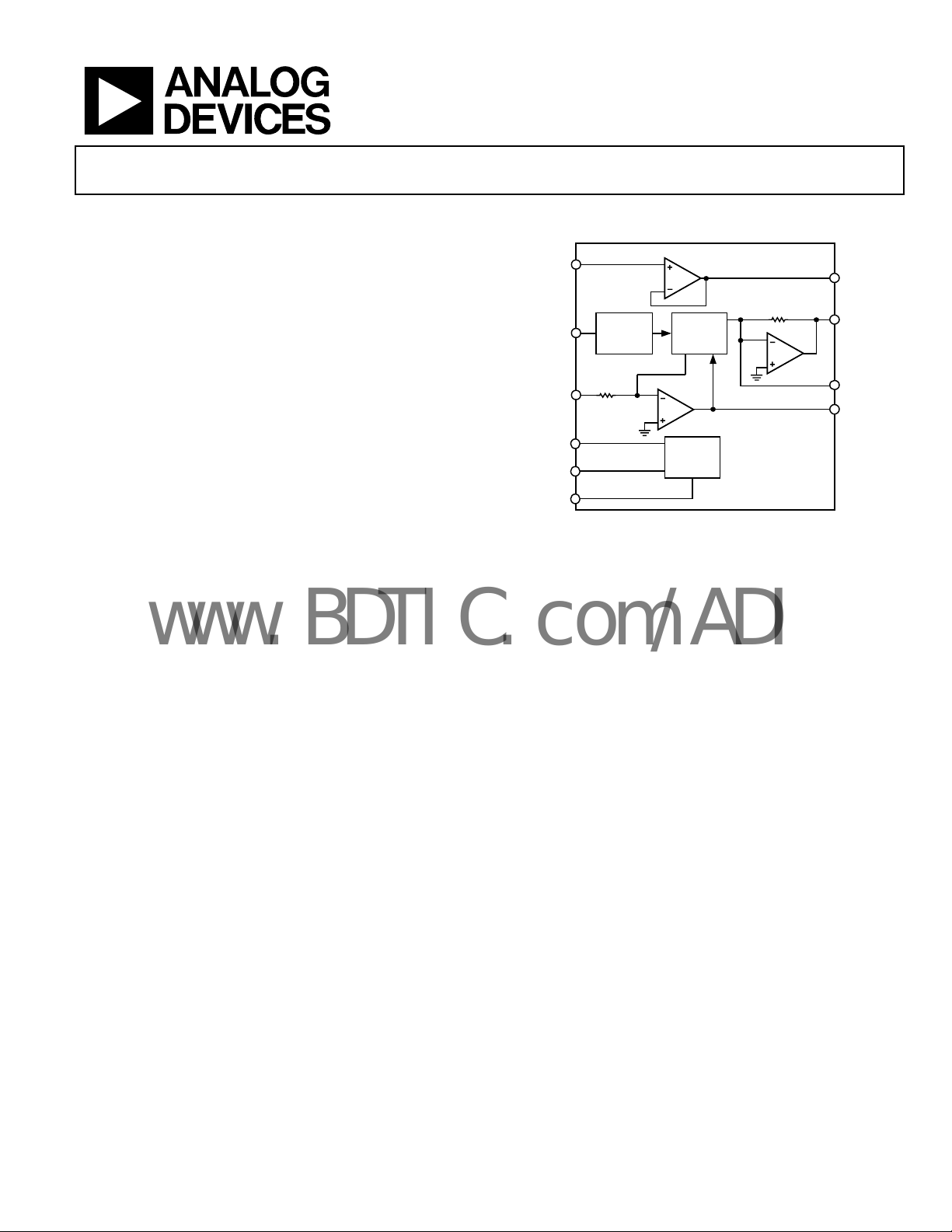
BUFF IN
DEN INPUT
OUTPUT
OFFSET
COMMON
RMS-to-DC Converter
FUNCTIONAL BLOCK DIAGRAM
V
CS
ABSOLUTE
IN
VALUE
25k
SQUARER/
DIVIDE R
BIAS
Figure 1.
25k
AD637
AD637
BUFF
OUT
RMS OUT
C
AV
dB OUTPUT
00788-001
The AD637 is a complete, high accuracy, monolithic rms-to-dc
converter that computes the true rms value of any complex
waveform. It offers performance that is unprecedented in
integrated circuit rms-to-dc converters and comparable to
discrete and modular techniques in accuracy, bandwidth, and
dynamic range. A crest factor compensation scheme in the
AD637 permits measurements of signals with crest factors of
up to 10 with less than 1% additional error. The wide bandwidth of the AD637 permits the measurement of signals up to
600 kHz with inputs of 200 mV rms and up to 8 MHz when the
input levels are above 1 V rms.
As with previous monolithic rms converters from Analog
vices, Inc., the AD637 has an auxiliary dB output available to
De
users. The logarithm of the rms output signal is brought out to a
separate pin, allowing direct dB measurement with a useful
range of 60 dB. An externally programmed reference current
allows the user to select the 0 dB reference voltage to correspond to
any level between 0.1 V and 2.0 V rms.
A chip select connection on the AD637 permits the user to
ease the supply current from 2.2 mA to 350 μA during periods
decr
when the rms function is not in use. This feature facilitates the
addition of precision rms measurement to remote or handheld
applications where minimum power consumption is critical. In
addition, when the AD637 is powered down, the output goes to a
high impedance state. This allows several AD637s to be tied
together to form a wideband true rms multiplexer.
Rev. J
Information furnished by Analog Devices is believed to be accurate and reliable. However, no
responsibility is assumed by Anal og Devices for its use, nor for any infringements of patents or ot her
rights of third parties that may result from its use. Specifications subject to change without notice. No
license is granted by implication or otherwise under any patent or patent rights of Analog Devices.
Trademarks and registered trademarks are the property of their respective owners.
The input circuitry of the AD637 is protected from overload
oltages in excess of the supply levels. The inputs are not
v
damaged by input signals if the supply voltages are lost.
The AD637 is available in accuracy Grade J and Grade K for
mmercial temperature range (0°C to 70°C) applications, accuracy
co
Grade A and Grade B for industrial range (−40°C to +85°C) applications, and accuracy Grade S rated over the −55°C to +125°C
temperature range. All versions are available in hermetically sealed,
14-lead SBDIP, 14-lead CERDIP, and 16-lead SOIC_W packages.
The AD637 computes the true root mean square, mean square,
o
r absolute value of any complex ac (or ac plus dc) input
waveform and gives an equivalent dc output voltage. The true
rms value of a waveform is more useful than an average
rectified signal because it relates directly to the power of the
signal. The rms value of a statistical signal is also related to the
standard deviation of the signal.
The AD637 is laser wafer trimmed to achieve rated performance
ithout external trimming. The only external component
w
required is a capacitor that sets the averaging time period. The
value of this capacitor also determines low frequency accuracy,
ripple level, and settling time.
The on-chip buffer amplifier can be used either as an input
uffer or in an active filter configuration. The filter can be used
b
to reduce the amount of ac ripple, thereby increasing accuracy.
One Technology Way, P.O. Box 9106, Norwood, MA 02062-9106, U.S.A.
Tel: 781.329.4700 www.analog.com
Fax: 781.461.3113 ©2007 Analog Devices, Inc. All rights reserved.

AD637
www.BDTIC.com/ADI
TABLE OF CONTENTS
Features .............................................................................................. 1
Choosing the Averaging Time Constant....................................9
Functional Block Diagram .............................................................. 1
General Description......................................................................... 1
Revision History ............................................................................... 2
Specifications..................................................................................... 3
Absolute Maximum Ratings............................................................ 5
ESD Caution.................................................................................. 5
Pin Configurations and Function Descriptions ........................... 6
Functional Description ....................................................................7
Standard Connection ................................................................... 8
Chip Select..................................................................................... 8
Optional Trims for High Accuracy............................................ 8
REVISION HISTORY
4/07—Rev. I to Rev. J
Added Evaluation Board Section ................................................. 16
Updated Outline Dimensions....................................................... 20
10/06—Rev. H to Rev. I
hanges to Table 1............................................................................ 3
C
Changes to Figure 4.......................................................................... 7
Changes to Figure 7.......................................................................... 9
Changes to Figure 16, Figure 18, and Figure 19......................... 12
Changes to Figure 20...................................................................... 13
12/05—Rev. G to Rev. H
pdated Format..................................................................Universal
U
Changes to Figure 1.......................................................................... 1
Changes to Figure 11...................................................................... 10
Updated Outline Dimensions....................................................... 16
Changes to Ordering Guide.......................................................... 17
Frequency Response .................................................................. 11
AC Measurement Accuracy and Crest Factor........................ 12
Connection for dB Output........................................................ 12
dB Calibration............................................................................. 13
Low Frequency Measurements................................................. 14
Vector Summation ..................................................................... 14
Evaluation Board ............................................................................ 16
Outline Dimensions ....................................................................... 19
Ordering Guide .......................................................................... 20
4/05—Rev. F to Rev. G
pdated Format..................................................................Universal
U
Changes to Figure 1...........................................................................1
Changes to General Description .....................................................1
Deleted Product Highlights .............................................................1
Moved Figure 4 to Page ....................................................................8
Changes to Figure 5...........................................................................9
Changes to Figure 8........................................................................ 10
Changes to Figure 11, Figure 12, Figure 13, and Figure 14....... 11
Changes to Figure 19...................................................................... 14
Changes to Figure 20...................................................................... 14
Changes to Figure 21...................................................................... 16
Updated Outline Dimensions....................................................... 17
Changes to Ordering Guide.......................................................... 18
3/02—Rev. E to Rev. F
dits to Ordering Guide...................................................................3
E
Rev. J | Page 2 of 20
AD637
www.BDTIC.com/ADI
SPECIFICATIONS
At 25°C and ±15 V dc, unless otherwise noted.
Table 1.
AD637J/AD637A AD637K/AD637B AD637S
Parameter Min Typ Max Min Typ Max Min Typ Max Unit
TRANSFER FUNCTION
CONVERSION ACCURACY
Total Error, Internal Trim2
(Figure 5)
T
to T
MIN
vs. Supply
vs. Supply
DC Reversal
Nonlinearity 2 V Full Scale3
Nonlinearity 7 V Full Scale
Total Error, External Trim ±0.5 ± 0.1 ±0.25 ± 0.05 ±0.5 ± 0.1 mV ± % of
ERROR VS. CREST FACTOR
Crest Factor 1 to 2 Specified accuracy Specified accuracy Specified accuracy
Crest Factor = 3 ±0.1 ±0.1 ±0.1 % of
Crest Factor = 10 ±1.0 ±1.0 ±1.0 % of
AVERAGING TIME CONSTANT 25 25 25 ms/μF C
INPUT CHARACTERISTICS
Signal Range, ±15 V Supply
Continuous RMS Level 0 to 7 0 to 7 0 to 7 V rms
Peak Transient Input ±15 ±15 ±15 V p-p
Signal Range, ±5 V Supply
Continuous RMS Level 0 to 4 0 to 4 0 to 4 V rms
Peak Transient Input ±6 ±6 ±6 V p-p
Maximum Continuous
Nondestructive
Input Level
(All Supply Voltages)
Input Resistance 6.4 8 9.6 6.4 8 9.6 6.4 8 9.6 kΩ
Input Offset Voltage ±0.5 ±0.2 ±0.5 mV
FREQUENCY RESPONSE5
Bandwidth for 1%
Additional Error
(0.09 dB)
VIN = 20 mV 11 11 11 kHz
VIN = 200 mV 66 66 66 kHz
VIN = 2 V 200 200 200 kHz
±3 dB Bandwidth
VIN = 20 mV 150 150 150 kHz
VIN = 200 mV 1 1 1 MHz
VIN = 2 V 8 8 8 MHz
MAX
= 300 mV
+V
IN
= −300 mV
−V
IN
Error at 2 V
4
V
=
OUT
30
100
±15 ±15 ±15 V p-p
1
2
)(V avg × V
IN
±1 ± 0.5 ±0.5 ± 0.2 ±1 ± 0.5
±3.0 ± 0.6 ±2.0 ± 0.3 ±6 ± 0.7
150
300
0.25
0.04
0.05
30
100
OUT
=
2
)(V avg × V
IN
150
300
0.1
0.02
0.05
30
100
OUT
=
)(V avg ×
IN
2
150
300
0.25
0.04
0.05
mV ±% of
re
ading
mV ± % of
reading
μV/V
μV/V
% of
reading
% of FSR
% of FSR
reading
reading
reading
AV
Rev. J | Page 3 of 20

AD637
www.BDTIC.com/ADI
AD637J/AD637A AD637K/AD637B AD637S
Parameter Min Typ Max Min Typ Max Min Typ Max Unit
OUTPUT CHARACTERISTICS
Offset Voltage
vs. Temperature ±0.05
Voltage Swing,
0 to 12.0
13.5
±1
±0.089
±15 V Supply, 2 kΩ Load
Voltage Swing,
0 to 2
2.2
±3 V Supply, 2 kΩ Load
Output Current
6
Short-Circuit Current 20 20 20 mA
Resistance
0.5 0.5 0.5 Ω
Chip Select High
Resistance
100 100 100 kΩ
Chip Select Low
dB OUTPUT
Error, VIN 7 mV to 7 V rms,
±0.5 ±0.3 ±0.5 dB
0 dB = 1 V rms
Scale Factor −3 −3 −3 mV/dB
Scale Factor Temperature
+0.33 +0.33 +0.33 % of
Coefficient
−0.033 −0.033 −0.033 dB/°C
I
for 0 dB = 1 V rms 5 20
REF
I
Range 1 100 1 100 1 100 μA
REF
80
BUFFER AMPLIFIER
Input Output
−VS to (+VS − 2.5 V) −VS to (+VS − 2.5 V) −VS to (+VS − 2.5 V) V
Voltage Range
Input Offset Voltage ±0.8
Input Current ±2
Input Resistance 10
8
±2
±10
10
Output Current −0.13 +5 −0.13 +5 −0.13 +5 mA
Short-Circuit Current 20 20 20 mA
Small Signal Bandwidth 1 1 1 MHz
Slew Rate
6
5 5 5 V/μs
DENOMINATOR INPUT
Input Range 0 to 10 0 to 10 0 to 10 V
Input Resistance 20 25 30 20 25 30 20 25 30 kΩ
Offset Voltage ±0.2 ±0.5 ±0.2 ±0.5 ±0.2 ±0.5 mV
CHIP SELECT (CS)
RMS On Level Open or 2.4 V < VC < +V
RMS Off Level VC < 0.2 V VC < 0.2 V VC < 0.2 V
I
of Chip Select
OUT
CS Low 10 10 10 μA
CS High 0 0 0 μA
On Time Constant 10 + ((25 kΩ) × CAV) 10 + ((25 kΩ) × CAV) 10 + ((25 kΩ) × CAV) μs
Off Time Constant 10 + ((25 kΩ) × CAV) 10 + ((25 kΩ) × CAV) 10 + ((25 kΩ) × CAV) μs
POWER SUPPLY
Operating Voltage Range
±3.0
Quiescent Current 2.2
Standby Current 350
1
Specifications shown in bold are tested on all production units at final electrical test. Results from those tests are used to calculate outgoing quality levels.
All minimum and maximum specifications are guaranteed, although only those shown in boldface are tested on all production units.
2
Accuracy specified 0 V rms to 7 V rms dc with AD637 connected, as shown in Figure 5.
3
Nonlinearity is defined as the maximum deviation from the straight line connecting the readings at 10 mV and 2 V.
4
Error vs. crest factor is specified as additional error for 1 V rms.
5
Input voltages are expressed in volts rms. Percent is in % of reading.
6
With external 2 kΩ pull-down resistor tied to −VS.
±18 ±3.0
3
450
±0.04
0 to 12.0
0 to 2
6
5 20
±0.5
±2
S
Open or 2.4 V < VC < +V
2.2
350
±0.5
±0.056
13.5
2.2
80
±1
±5
8
10
S
±18 ±3.0
3
450
±0.04
0 to 12.0
0 to 2
6
13.5 V
2.2 V
mA
5 20
±0.8
±2
8
±1
±0.07
80
±2
±10
Ω
Open or 2.4 V < VC < +V
2.2
350
±18
3
450
S
mV
mV/°C
reading/°C
μA
mV
nA
V
mA
μA
Rev. J | Page 4 of 20
AD637
www.BDTIC.com/ADI
ABSOLUTE MAXIMUM RATINGS
Table 2.
Parameter Rating
ESD Rating 500 V
Supply Voltage ±18 V dc
Internal Quiescent Power Dissipation 108 mW
Output Short-Circuit Duration Indefinite
Storage Temperature Range −65°C to +150°C
Lead Temperature (Soldering 10 sec) 300°C
Rated Operating Temperature Range
AD637J, AD637K 0°C to 70°C
AD637A, AD637B −40°C to +85°C
AD637S, 5962-8963701CA −55°C to +125°C
Stresses above those listed under Absolute Maximum Ratings
may cause permanent damage to the device. This is a stress
rating only; functional operation of the device at these or any
other conditions above those indicated in the operational
section of this specification is not implied. Exposure to absolute
maximum rating conditions for extended periods may affect
device reliability.
ESD CAUTION
Rev. J | Page 5 of 20
AD637
T
www.BDTIC.com/ADI
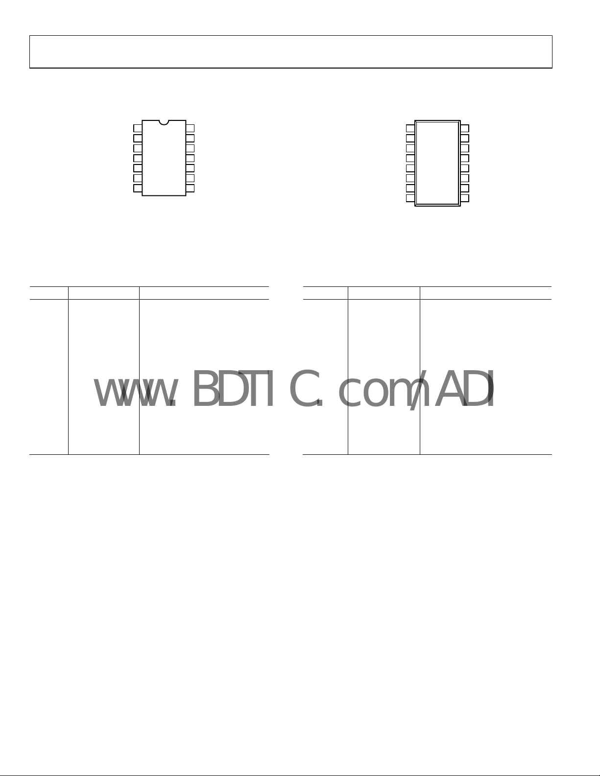
PIN CONFIGURATIONS AND FUNCTION DESCRIPTIONS
1
BUFF IN
NC
2
COMMON
OUTPUT OFFSET
DEN INPUT
dB OUTPUT
3
AD637
TOP VIEW
4
(Not to Scale)
5
CS
6
7
NC = NO CONNECT
Figure 2. 14-Lead SBDIP/CERDIP Pin Configuration
14
BUFF OUT
V
13
NC
12
+V
11
10
–V
9
RMS OUT
C
8
BUFF IN
1
NC
IN
S
S
AV
00788-002
COMMON
OUTPUT OFFSET
DEN INPUT
dB OUTPUT
2
3
AD637
4
TOP VIEW
(Not to Scale)
5
CS
6
7
NC
8
NC = NO CONNECT
BUFF OU
16
V
15
NC
14
13
+V
12
–V
11
RMS OUT
C
10
NC
9
IN
S
S
AV
00788-003
Figure 3. 16-Lead SOIC_W Pin Configuration
Table 3. 14-Lead SBDIP/CERDIP Pin Function Descriptions Table 4. 16-Lead SOIC_W Pin Function Descriptions
Pin No. Mnemonic Description Pin No. Mnemonic Description
1 BUFF IN Buffer Input 1 BUFF IN Buffer Input
2, 12 NC No Connection
3 COMMON Analog Common
4 OUTPUT OFFSET Output Offset
5 CS Chip Select
6 DEN INPUT Denominator Input
7 dB OUTPUT dB Output
8 C
AV
Averaging Capacitor Connection
9 RMS OUT RMS Output
10 −V
11 +V
13 V
S
S
IN
Negative Supply Rail
Positive Supply Rail
Signal Input
14 BUFF OUT Buffer Output
2, 8, 9, 14 NC No Connection
3 COMMON
4 OUTPUT OFFSET
5 CS
6 DEN INPUT
7 dB OUTPUT
10 C
AV
11 RMS OUT
12 −V
13 +V
15 V
S
S
IN
Analog Common
Output Offset
Chip Select
Denominator Input
dB Output
Averaging Capacitor Connection
RMS Output
Negative Supply Rail
Positive Supply Rail
Signal Input
16 BUFF OUT Buffer Output
Rev. J | Page 6 of 20

AD637
www.BDTIC.com/ADI
FUNCTIONAL DESCRIPTION
I
4
A3
125
FILTER/AMPLIF IER
24k
A4
Q5
BIAS
I
24k
3
AD637
BUFF OUT
BUFF IN
V
14
1
24k
ABSOLUTE VALUE VOLTAGE TO
CURRENT CONVERTE R
6k
12k
13
IN
A1
ONE QUADRANT
SQUARER/DIVI DER
Q1
Q2
Q4
Q3
6k
BUFFER
AMPLIFIER
I
1
A2
A5
Figure 4. Simplified Schematic
8
C
+V
11
RMS
9
OUT
dB
7
OUTPUT
3
COMMON
CS
5
DEN
6
INPUT
OUTPUT
4
OFFSET
–V
10
AV
S
S
00788-004
The AD637 embodies an implicit s
olution of the rms equation
that overcomes the inherent limitations of straightforward rms
computation. The actual computation performed by the AD637
follows the equation
2
⎤
⎡
V
=
AvgrmsV
IN
⎥
⎢
rmsV
⎥
⎢
⎦
⎣
Figure 4 is a simplified schematic of the AD637, subdivided
into four major sections: absolute value circuit (active rectifier),
squarer/divider, filter circuit, and buffer amplifier. The input
voltage (V
current I
), which can be ac or dc, is converted to a unipolar
IN
by the active rectifiers A1 and A2. I1 drives one input
1
of the squarer/divider, which has the transfer function
2
I
1
=
I
4
I
3
The output current of the squarer/divider I
drives A4, forming
4
a low-pass filter with the external averaging capacitor. If the RC
time constant of the filter is much greater than the longest period
of the input signal, then the A4 output is proportional to the
average of I
to provide the denominator current I
. The output of this filter amplifier is used by A3
4
, which equals Avg I4 and
3
is returned to the squarer/divider to complete the implicit rms
computation
2
⎤
⎡
I
1
AvgI
=
4
=
⎥
⎢
I
4
⎦
⎣
rmsI
1
To compute the absolute value of the input signal, the averaging
pacitor is omitted. However, a small capacitance value at the
ca
averaging capacitor pin is recommended to maintain stability;
5 pF is sufficient for this purpose. The circuit operates identically
to that of the rms configuration, except that I
I
, giving
4
2
I
1
I =
I = |I |
4 1
4
I
4
is now equal to
3
The denominator current can also be supplied externally by
providing a reference voltage (V
identically to the rms case, except that I
V . Therefore,
REF
2
I
1
Avg
I =
4
I
3
) to Pin 6. The circuit operates
REF
is now proportional to
3
and
2
V
V
OUT
IN
=
V
DEN
This is the mean square of the input signal.
and
V
= VIN rms
OUT
Rev. J | Page 7 of 20

AD637
www.BDTIC.com/ADI
STANDARD CONNECTION
The AD637 is simple to connect for a majority of rms
measurements. In the standard rms connection shown in Figure 5,
o
nly a single external capacitor is required to set the averaging
time constant. In this configuration, the AD637 computes the
true rms of any input signal. An averaging error, the magnitude
of which is dependent on the value of the averaging capacitor,
is present at low frequencies. For example, if the filter capacitor,
C
, is 4 μF, the error is 0.1% at 10 Hz and increases to 1% at
AV
3 Hz. To measure ac signals, the AD637 can be ac-coupled by
adding a nonpolar capacitor in series with the input, as shown
in Figure 5.
4.7k
1
BUFF IN
2NC
3 COMMON
+V
S
OUTPUT
4
OFFSET
CS
5
DEN
25k
INPUT
6
7 8
dB OUTPUT
BIAS
AD637
SQUARER/
DIVIDER
ABSOLUTE
VALUE
25k
BUFF
OUT
V
+V
–V
C
IN
S
S
AV
14
NC
13
12NC
(OPTIONAL)
11
+V
10
–V
V
9
C
+
AV
S
S
OUT
V
IN
=V
20
15
10
(Volts 2k Load)
OUT
5
MAX V
0
±3 ±5 ±10 ±15 ±18
0
SUPPLY VOL TAGE – DUAL SUPPLY (V)
Figure 6. Maximum V
vs. Supply Voltage
OUT
00788-006
CHIP SELECT
The AD637 includes a chip select feature that allows the user
to decrease the quiescent current of the device from 2.2 mA to
350 μA. This is done by driving CS, Pin 5, to below 0.2 V dc.
Under these conditions, the output goes into a high impedance
state. In addition to reducing the power consumption,
2
IN
the outputs of multiple devices can be connected in parallel
to form a wide bandwidth rms multiplexer. Tie Pin 5 high to
disable the chip select.
00788-005
Figure 5. Standard RMS Connection
The performance of the AD637 is tolerant of minor variations
he power supply voltages; however, if the supplies used
in t
exhibit a considerable amount of high frequency ripple, it is
advisable to bypass both supplies to ground through a 0.1 μF
ceramic disc capacitor placed as close to the device as possible.
The output signal range of the AD637 is a function of the
su
pply voltages, as shown in Figure 6. The output signal can be
us
ed buffered or nonbuffered, depending on the characteristics
of the load. If no buffer is needed, tie the buffer input (Pin 1) to
common. The output of the AD637 is capable of driving 5 mA
into a 2 kΩ load without degrading the accuracy of the device.
The AD637 includes provisions for trimming out output offset
and scale factor errors resulting in significant reduction in the
maximum total error, as shown in
Figure 7. The residual error is
due to a nontrimmable input offset in the absolute value circuit
and the irreducible nonlinearity of the device.
Referring to Figure 8, the trimming process is as follows:
• Offset trim: Ground the input signal (V
) and adjust R1 to
IN
give 0 V output from Pin 9. Alternatively, R1 can be adjusted
to give the correct output with the lowest expected value of V .
IN
• Scale factor trim: Resistor R4 is inserted in series with the
input to lower the range of the scale factor. Connect the
desired full-scale input to V
, using either a dc or a calibrated ac
IN
signal, and trim Resistor R3 to give the correct output at Pin 9
(that is, 1 V dc at the input results in a dc output voltage of
l.000 V dc). A 2 V p-p sine wave input yields 0.707 V dc at the
output. Remaining errors are due to the nonlinearity.
OPTIONAL TRIMS FOR HIGH ACCURACY
Rev. J | Page 8 of 20

AD637
5
www.BDTIC.com/ADI
OUTPUT
OFFSET
TRIM
+V
S
R1
0k
–V
S
5.0
2.5
0
ERROR (mV)
–2.5
AD637K: 0.5mV ± 0.2%
0.25mV ± 0.05%
EXTERNAL
–5.0
00.5
Input Le
R2
1M
4.7k
+V
S
AD637K MAX
INTERNAL TRIM
AD637K
EXTERNAL T RIM
1.0
INPUT LEVEL (V)
1.5 2.0
Figure 7. Maximum Total Error vs.
vel AD637K Internal and External Trims
BIAS
AD637
SQUARER/
DIVIDER
ABSOLUTE
VALUE
25k
BUFF
OUT
+V
–V
C
V
IN
S
S
AV
1
BUFF IN
2NC
3COMMON
OUTPUT
4
OFFSET
CS
5
DEN
25k
6
INPUT
dB OUTPUT
7 8
00788-007
14
NC
R4
V
147
IN
13
12NC
11
+V
S
10
–V
S
2
V
=V
OUT
9
C
+
IN
AV
E
O
DOUBLE-FREQ UENCY
RIPPLE
IDEAL
E
O
DC ERROR = AVERAGE OF OUTP UT – IDEAL
AVERAGE ERROR
TIME
00788-009
Figure 9. Typical Output Waveform for a Sinusoidal Input
This ripple can add a significant amount of uncertainty to the
accuracy of the measurement being made. The uncertainty can
be significantly reduced through the use of a postfiltering
network or by increasing the value of the averaging capacitor.
The dc error appears as a frequency dependent offset at the
output of the AD637 and follows the relationship
1
22
f
4.616.0
τ+
Because the averaging time constant, set by C
readingof%in
, directly sets
AV
the time that the rms converter holds the input signal during
computation, the magnitude of the dc error is determined only
by C and is not affected by postfiltering.
AV
100
SCALE FACT OR TRIM
Figure 8. Optional External
R3
1k
Gain and Offset Trims
00788-008
CHOOSING THE AVERAGING TIME CONSTANT
The AD637 computes the true rms value of both dc and ac
input signals. At dc, the output tracks the absolute value of the
input exactly; with ac signals, the AD637 output approaches the
true rms value of the input. The deviation from the ideal rms
value is due to an averaging error. The averaging error
comprises an ac component and a dc component. Both
components are functions of input signal frequency f and the
averaging time constant τ (τ: 25 ms/μF of averaging capacitance).
Figure 9 shows that the averaging error is defined as the peak
val
ue of the ac component (ripple) and the value of the dc error.
The peak value of the ac ripple component of the averaging
er
ror is defined approximately by the relationship
50
f1ττ6.3
()
fwherereadingof%in
>
10
1.0
DC ERROR
DC ERROR OR RIPPL E (% of Readi ng)
0.1
10
SINE WAVE INPUT FREQUENCY (Hz)
PEAK RIP PLE
1k100
10k
00788-010
Figu re 10. Comparison of Percent DC Error to the Percent Peak Ripple over
Frequency
Using the AD637 in the Standard RMS Connection with a 1 × μF C
AV
The ac ripple component of averaging error is greatly reduced
by increasing the value of the averaging capacitor. There are two
major disadvantages to this: the value of the averaging capacitor
becomes extremely large and the settling time of the AD637
increases in direct proportion to the value of the averaging
capacitor (T
= 115 ms/μF of averaging capacitance). A preferable
S
method of reducing the ripple is by using the postfilter network,
as shown in
ole or 2-pole configuration. For most applications, the 1-pole
p
Figure 11. This network can be used in either a 1-
filter gives the best overall compromise between ripple and
settling time.
Rev. J | Page 9 of 20

AD637
www.BDTIC.com/ADI
BIAS
AD637
SQUARER/
DIVIDER
RX
24k
ABSOLUTE
VALUE
25k
BUFF
OUT
14 RMS OUT
V
IN
13
V
IN
+
12NC
11
+V
+V
S
S
10
–V
–V
S
S
9
C
+
AV
C
AV
24k
FOR A SINGL E-POLE
FILTER SHORT RX
AND REMOVE C3
C3
1
BUFF IN
2NC
3COMMON
OUTPUT
4
OFFSET
+V
S
4.7k
CS
5
DEN
25k
INPUT
6
7 8
dB OUTPUT
+
C2
Figure 11. 2-Pole Sallen-Key Filter
Figure 12 shows values of CAV and the corresponding averaging
error as a function of sine wave frequency for the standard rms
connection. The 1% settling time is shown on the right side of
Figure 12.
Figure 13 shows the relationship between the averaging error,
ignal frequency settling time, and averaging capacitor value.
s
Figure 13 is drawn for filter capacitor values of 3.3× the
veraging capacitor value. This ratio sets the magnitude of the
a
ac and dc errors equal at 50 Hz. As an example, by using a 1 μF
averaging capacitor and a 3.3 μF filter capacitor, the ripple for
a 60 Hz input signal is reduced from 5.3% of the reading using
the averaging capacitor alone to 0.15% using the 1-pole filter.
This gives a factor of 30 reduction in ripple, and yet the settling
time only increases by a factor of 3. The values of filter
Capacitor C
and Filter Capacitor C2 can be calculated for
AV
the desired value of averaging error and settling time by using
Figure 13.
The symmetry of the input signal also has an effect on the
ma
gnitude of the averaging error. Tab le 5 gives the practical
co
mponent values for various types of 60 Hz input signals.
These capacitor values can be directly scaled for frequencies
other than 60 Hz—that is, for 30 Hz, these values are doubled,
and for 120 Hz they are halved.
For applications that are extremely sensitive to ripple, the 2-pole
nfiguration is suggested. This configuration minimizes capacitor
co
values and the settling time while maximizing performance.
Figure 14 can be used to determine the required value of CAV,
C2, and C3 for the desired level of ripple and settling time.
100
ERR
O
1
%
R
0.1%
ERROR
10
(µF)
AV
1.0
REQUIRED C
0.1
*%dc ERROR + %RIPPLE (PEAK)
0.01
1 100k10 100 1k 10k
Figure 12. Values for C
1
0%
INPUT FREQUENCY (Hz)
and 1% Settling Time for Stated % of Reading Averaging
AV
0.01% ERROR
E
RROR
100
10
1.0
0.1
0.01
MULTIPLY READING BY 0.115
FOR 1% SETTLING TIME IN SECONDS
00788-012
Error* Accuracy Includes ±2% Component Tolerance (see * in Figure)
00788-011
100
10
AV
(AND C2)
AV
1
C2 = 3.3 × C
REQUIRED C
0.1
0.01
1 100k10 100 1k 10k
Figure 13. Values of C
, C2, and 1% Settling Time for Stated % of Reading
AV
*%dc ERROR + %RIPPLE (PEAK)
ACCURACY ±20% DUE TO
COMPONENT T OLERANCE
0.01%
0
.1%
E
ERRO
1%
ERRO
5%
E
RR
R
O
R
INPUT FREQ UENCY (Hz)
100
10
RR
O
R
R
1
0.1
0.01
MULTIPL Y READING BY 0.400
FOR 1% SETTLING TIME IN SECONDS
00788-013
Averaging Error* for 1-Pole Post Filter (see * in Figure)
100
10
AV
(AND C2 + C3)
1
AV
C2 = C3 = 2.2 × C
0.1
REQUIRED C
*%dc ERROR + % RIPPLE (PEAK)
ACCURACY ±20% DUE TO
COMPO NENT TOLERA NCE
0.01
1110
Figure 14. Values of C
0
.
01
%
0.1% ERROR
ERROR
1
%
ERR
5
%
ERROR
O
R
100 1k 10k
INPUT FREQ UENCY (Hz)
, C2, and C3 and 1% Settling Time for Stated % of
AV
100
10
1
0.1
MULTIPL Y READING BY 0.365
FOR 1% SETT LING TIME IN SECO NDS
0.01
00k
00788-014
Reading Averaging Error* for 2-Pole Sallen-Key Filter (see * in Figure)
Rev. J | Page 10 of 20

AD637
www.BDTIC.com/ADI
Table 5. Practical Values of CAV and C2 for Various Input Waveforms
Absolute Value
Input Waveform
and P
eriod
T
A
Symmetrical Sine Wave
T
B
Sine Wave with dc Offset
T
C
D
T
2
Pulse Train Waveform
T
T
2
Circuit Waveform
and Period
0V
0V
0V
0V
1/2T
T
T
T
2
T
T
2
Minimum R × CAV
Time Constant
1/2T 0.47 1.5 181 ms
T 0.82 2.7
10 (T − T
) 6.8 22 2.67 sec
2
10 (T − 2T
) 5.6 18 2.17 sec
2
FREQUENCY RESPONSE
The frequency response of the AD637 at various signal levels is
shown in Figure 15. The dashed lines show the upper frequency
limits fo
note that for 1% additional error with a 2 V rms input, the
highest frequency allowable is 200 kHz. A 200 mV signal can
be measured with 1% error at signal frequencies up to 100 kHz.
To take full advantage of the wide bandwidth of the AD637,
ca
To ensure that the input signal is accurately presented to the
converter, the input buffer must have a −3 dB bandwidth that is
wider than that of the AD637. Note the importance of slew rate
in this application. For example, the minimum slew rate required
for a 1 V rms, 5 MHz, sine wave input signal is 44 V/μs. The user is
cautioned that this is the minimum rising or falling slew rate
and that care must be exercised in the selection of the buffer
amplifier, because some amplifiers exhibit a two-to-one
difference between rising and falling slew rates. The AD845 is
recommended as a precision input buffer.
r 1%, 10%, and ±3 dB of additional error. For example,
re must be taken in the selection of the input buffer amplifier.
Recommended Standard Values for CAV and C2
for 1% Averaging Error @ 60 Hz with T = 16.6 ms
(μF) C2 (μF) C
AV
10
7V RMS INPUT
2V RMS INPUT
1V RMS INPUT
1
V)
(
OUT
100mV RMS INPUT
V
0.1
0.01
100mV RMS INPUT
1k 10M10k
INPUT FREQ UENCY (Hz)
Figure 15. Frequency Response
1%
10%
100k 1M
1% Settling
ime
T
325 ms
±3dB
00788-015
Rev. J | Page 11 of 20

AD637
0
www.BDTIC.com/ADI
AC MEASUREMENT ACCURACY AND CREST FACTOR
Crest factor is often overlooked in determining the accuracy of
an ac measurement. Crest factor is defined as the ratio of the peak
signal amplitude to the rms value of the signal (CF = V
Most common waveforms, such as sine and triangle waves, have
relatively low crest factors (≤2). Waveforms that resemble low
duty cycle pulse trains, such as those occurring in switching
power supplies and SCR circuits, have high crest factors. For
example, a rectangular pulse train with a 1% duty cycle has
a crest factor of 10 (CF = 1
Vp
100µF
Figure 16. Duty Cycle Timing
10
1
0.1
INCREASE IN ERROR (%)
0.01
1 100010
Figure 17. AD637 Error vs. Pulse Width Rectangular Pulse
T
e
0
PULSE WIDTH (µs)
η ).
= DUTY CYCLE =
CF = 1/
e
(RMS) = 1 V RMS
IN
CAV = 22µF
100
Figure 18 is a curve of additional reading error for the AD637
r a 1 V rms input signal with crest factors from 1 to 11.
fo
A rectangular pulse train (pulse width 100 μs) is used for this
test because it is the worst-case waveform for rms measurement
(all the energy is contained in the peaks). The duty cycle and
peak amplitude were varied to produce crest factors from l to 10
while maintaining a constant 1 V rms input amplitude.
100µs
T
CF = 10
CF = 3
/V rms).
P
00788-016
00788-017
1.5
1.0
0.5
0
–0.5
POSITIVE I NPUT PULSE
INCREASE IN ERROR (%)
–1.0
–1.5
112
C
= 22µF
AV
3 78910
456
CREST FACTOR
1
0788-018
Figure 18. Additional Error vs. Crest Factor
2.0
1.8
1.6
1.4
1.2
1.0
0.8
0.6
0.4
0.2
MAGNITUDE OF ERROR (% of RMS Level)
0
0
CF = 10
CF = 7
CF = 3
VIN (V RMS)
2.00.5 1.0 1.5
00788-019
Figure 19. Error vs. RMS Input Level for Three Common Crest Factors
CONNECTION FOR dB OUTPUT
Another feature of the AD637 is the logarithmic, or decibel,
output. The internal circuit that computes dB works well over
a 60 dB range.
The us
reference current, which is set to cancel the log output current
from the squarer/divider circuit at the desired 0 dB point. The
external op amp is used to provide a more convenient scale and to
allow compensation of the +0.33%/°C temperature drift of the
dB circuit. The temperature resistor R3, as shown in
i
s available from Precision Resistor Co., Inc., in Largo, Fla.
(Model PT146). Consult its website for additional information.
Figure 20 shows the dB measurement connection.
er selects the 0 dB level by setting R1 for the proper 0 dB
Figure 20,
Rev. J | Page 12 of 20

AD637
www.BDTIC.com/ADI
dB CALIBRATION
Refer to Figure 20:
• Set V
= 1.00 V dc or 1.00 V rms
IN
• Adjust R1 for 0 dB out = 0.00 V
• Set V = 0.1 V dc or 0.10 V rms
IN
• Adjust R2 for dB out = −2.00 V
Any other dB reference can be used by setting V
accordingly.
SIGNAL
INPUT
SECTION
25k
BUFFER
BIAS
+V
S
+V
10k
R1
500k
1
BUFF IN
2
NC
3
COMMON
OUTPUT
4
OFFSET
4.7k
5
6
7
+2.5 V
CS
DEN
INPUT
dB OUTPUT
S
and R1
IN
AD637
ABSOLUTE
SQUARER/DIVI DER
AD508J
VALUE
25k
FILTER
BUFF
OUT
14
V
13
IN
12
NC
11
+V
–V
C
NC = NO CONNECT
+V
S
10
–V
S
V
9
+
8
AV
OUT
S
S
1µF
R3
1k*
60.4
33.2k
2
3
R2
5k
+V
S
7
AD707JN
4
–V
S
dB SCALE
FACTOR
ADJUST
6
COMPENSATED
dB OUTPUT
+ 100mV/dB
0dB ADJUST
*1k + 3500ppm
SEE TEXT
00788-020
Figure 20. dB Connection
Rev. J | Page 13 of 20

AD637
V
www.BDTIC.com/ADI
3
2
6.8M
2
V+
7
AD548JN
4
V–
1000pF
6
FILTERED
RMS OUTPUT
0788-021
25k
BUFFER
BIAS
SECTION
C
3.3µF
BUFF IN
1
2
NC
COMMON
+V
S
4.7k
3
OUTPUT
OFFSET
4
CS
5
DEN
6
INPUT
7
dB OUTPUT
+V
S
OUTPUT
OFFSET
ADJUST
NOTES
1. VALUES CHO SEN TO G IVE 0.1% AV ERAGING E RROR @ 1Hz.
2. NC = NO CONNECT.
50k
1M
–V
S
Figure 21. AD637 as a Low Frequency RMS Converter
AD637
ABSOLUTE
VALUE
SQUARER/DIVI DER
FILTER
499k 1%
R
AV1
25k
BUFF
OUT
V
NC
+V
–V
C
1µF
3.3M
3.3M
+V
S
–V
OUT
100µF
SIGNAL
INPUT
S
1µF
V
IN
V RMS
14
IN
13
12
11
S
10
S
V
9
+
8
AV
LOW FREQUENCY MEASUREMENTS VECTOR SUMMATION
If the frequencies of the signals to be measured are below 10 Hz,
the value of the averaging capacitor required to deliver even 1%
averaging error in the standard rms connection becomes
extremely large.
taining low frequency rms measurements. The averaging
ob
time constant is determined by the product of R and C
this circuit, 0.5 sec/μF of C
Figure 21 shows an alternative method of
AV1
. This circuit permits a 20:1
AV
, in
reduction in the value of the averaging capacitor, permitting the
use of high quality tantalum capacitors. It is suggested that the
2-pole, Sallen-Key filter shown in
lo
w ripple level and minimize the value of the averaging
Figure 21 be used to obtain a
capacitor.
If the frequency of interest is below 1 Hz, or if the value of the
averaging capacitor is still too large, the 20:1 ratio can be
increased. This is accomplished by increasing the value of R.
If this is done, it is suggested that a low input current, low offset
voltage amplifier, such as the AD548, be used instead of the
internal buffer amplifier. This is necessary to minimize the
offset error introduced by the combination of amplifier input
currents and the larger resistance.
Vector summation can be accomplished through the use of two
AD637s, as shown in Figure 22. Here, the averaging capacitors
a
re omitted (nominal 100 pF capacitors are used to ensure
stability of the filter amplifier), and the outputs are summed as
shown. The output of the circuit is
22
VVV +=
OUT
YX
This concept can be expanded to include additional terms by
feedin
g the signal from Pin 9 of each additional AD637 through
a 10 kΩ resistor to the summing junction of the
t
ying all of the denominator inputs (Pin 6) together.
is added to IC1 in this configuration, then the output is If C
AV
22
VV +
YX
If the averaging capacitor is included on both IC1 and IC2, the
is
output
22
VV +
YX
This circuit has a dynamic range of 10 V to 10 mV and is
ited only by the 0.5 mV offset voltage of the AD637.
lim
The useful bandwidth is 100 kHz.
AD711 and
Rev. J | Page 14 of 20

AD637
www.BDTIC.com/ADI
BUFF I N
1
2
NC
3
COMMON
OUTPUT
OFFSET
4
+V
S
+V
S
4.7k
4.7k
CS
5
6
DEN
INPUT
7
dB OUTPUT
BUFF IN
1
NC
2
COMMON
3
OUTPUT
OFFSET
4
CS
5
DEN
INPUT
6
dB OUTPUT
7
25k
25k
BUFFER
BIAS
SECTION
BUFFER
BIAS
SECTION
EXPANDABLE
AD637
IC1
ABSOLUTE
SQUARER/DIVI DER
AD637
IC2
ABSOLUTE
SQUARER/DIVI DER
VALUE
FILTER
VALUE
FILTER
25k
25k
BUFF
OUT
VXIN
NC
+V
–V
V
OUT
BUFF
OUT
V
+V
–V
Y
NC
IN
S
S
S
S
14
13
12
11
10
9
100pF
8
10k
14
13
12
11
10
V
9
8
+V
–V
+V
–V
OUT
S
S
S
S
100pF
5pF
10k
AD711K
10k
20k
C
AV
2
V
=
OUT
2
V
+ V
X
Y
00788-022
Figure 22. Vector Sum Configuration
Rev. J | Page 15 of 20

AD637
www.BDTIC.com/ADI
EVALUATION BOARD
The evaluation board for the AD637 is shown in Figure 23. It is
available at www.analog.com and ships fully tested and ready
fo
r bench testing by just adding power and signal connections.
The circuit is configured for dual power supplies, and standard
BNC connectors serve as the signal input and output ports.
Figure 29Referring to the schematic in , the input BNC
RMS_IN
The BNC connector DC_OUT is connected to Pin 11, RMS
OUT, with provisions for connections to the output buffer
between Pin 1 and Pin 16. Users can connect the buffer using
components of their choice. A trimmer is available for adjusting
the output offset voltage. The board contains provisions for one
or two poles of low-pass filtering using CF1, CF2, R4, and R5.
See
is capacitively coupled to Pin 15 V
Figure 24 to locate these components.
of the AD637.
IN
00788-024
Figure 24. Evaluation Board—Component Side Silkscreen
00788-023
Figure 23. Evaluation Board
Figure 25. Evaluation Board—Component Side Copper
Rev. J | Page 16 of 20
00788-025

AD637
www.BDTIC.com/ADI
00788-026
Figure 26. Evaluation Board—S
econdary Side Copper
Figure 28. Evaluaiton Board—Internal Ground Plane
00788-028
00788-027
Figure 27. Evaluation Board—Internal Power Plane
Rev. J | Page 17 of 20

AD637
–V
V
)
www.BDTIC.com/ADI
Table 6. Evaluation Board Bill of Materials
Qty Name Description Reference Designator Manufacturer Mfg. Part Number
1 Test Loop Red +VS Components Corp. TP-104-01-02
1 Test Loop Green −VS Components Corp. TP-104-01-05
5 Test Loop Purple Components Corp.
BUF IN, BUF OUT, RMS IN,
DC OUT
, DB OUT
1 Header 3-pin BUF IN SEL Molex
2 Capacitor Tantalum 10 μF, 25 V C1, C2 Nichicon
2 Capacitor 0.1 μF, 16 V, 0603 X7R C3, C4 Kemet
1 Capacitor Tantalum 22 μF, 16 V CIN Nichicon
2 Connector BNC right angle RMS IN, DC OUT AMP
4 Test Loop Black GND1, GND2, GND3, GND4 Components Corp.
1 Resistor 1 MΩ, 5%, 1/10W, 0603 R1 Panasonic
1 Trimmer 50 kΩ, 6 mm sq SMD R2 Bourns
1 Resistor 4.75kΩ, 5%, 1/10W, 0603 R3 Panasonic
1 Header BERG 2 W1 Molex
1 Integrated Circuit RMS-to-dc converter Z1 Analog Devices, Inc. AD637ARZ
+
GND1 GND2 GND3 GND4
(BLACK TEST LOOP X4)
S
C1
+
10µF
25V
(GREEN TEST LOOP)
–V
S
S
C2
+
10µF
+V
(RED TEST LOOP)
25V
S
TP-104-01-07
22-10-2031
F931E106MCC
C0603C104K4RACTU
F931C226MCC
227161-1
TP-104-01-00
ERJ-3EKF1004V
3361S-1-503G
ERJ-3EKF4751V
22-10-2021
BUF IN
SEL
+
CF2
47µF
16V
(VIO LOOP TEST)
+V
S
R2
50k
–V
S
(VIO LOOP TEST)
GND
R1
1M
+V
S
DB OUT
R3
4.7k
1
BUF IN
2
NC
3
COMMON
4
OUTPUT
OFFSET
5
CS
6
DEN INPUT
7
dB OUTPUT
8
NC OTS-16-1.27-24
R4
24k
AD637
BUF OUT
V
NC
+V
–V
RMS OUT
C
AV
NC
16
15
IN
14
13
S
12
S
11
+
C
22µF
10
16V
9
24k
RMS IN
AV
R5
CIN
22µF
16V
+
C3
0.1µF
–V
+V
S
S
+
+
C4
0.1µF
BUF OUT
(VIO TEST LOOP
RMS IN
DC OUT
(VIO TEST
LOOP)
W1
+
CF1
47µF
16V
DC OUT
00788-029
BUF IN
FILTER
Figure 29. Evaluation Board Schematic
Rev. J | Page 18 of 20

AD637
C
R
.
www.BDTIC.com/ADI
OUTLINE DIMENSIONS
0.005 (0.13) MIN
PIN 1
0.200 (5.08)
MAX
0.200 (5.08)
0.125 (3.18)
ONTROLLING DIMENSIONS ARE IN INCHES; MILLIMETER DIMENSIONS
(IN PARENTHESES) ARE ROUNDED-OFF INCH EQUIVALENTS FO
REFERENCE ONLY AND ARE NOT APPROPRIATE FOR USE IN DESIGN
0.765 (19.43) MAX
0.023 (0.58)
0.014 (0.36)
Figure 30. 14-Lead Side-Brazed Ceram
14
1
0.100 (2.54)
0.080 (2.03) MAX
8
7
BSC
0.070 (1.78)
0.030 (0.76)
0.310 (7.87)
0.220 (5.59)
0.320 (8.13)
0.060 (1.52)
0.015 (0.38)
0.150
(3.81)
MIN
SEATING
PLANE
0.290 (7.37)
0.015 (0.38)
0.008 (0.20)
ic Dual In-Line Package [SBDIP]
(D-14)
Dimensions shown in inches and (millimeters)
0.005 (0.13) MIN
PIN 1
0.200 (5.08)
MAX
0.200 (5.08)
0.125 (3.18)
0.785 (19.94) MAX
0.023 (0.58)
0.014 (0.36)
0.098 (2.49) MAX
1
0.100 (2.54) BSC
0.070 (1.78)
0.030 (0.76)
814
7
0.310 (7.87)
0.220 (5.59)
0.060 (1.52)
0.015 (0.38)
0.150
(3.81)
MIN
SEATING
PLANE
0.320 (8.13)
0.290 (7.37)
15°
0°
0.015 (0.38)
0.008 (0.20)
CONTROLLING DIMENSIONS ARE IN INCHES; MILLIMETER DIMENSIONS
(IN PARENTHESES) ARE ROUNDED-OFF INCH EQUIVALENTS FOR
REFERENCE ONLY AND ARE NOT APPROPRIATE FOR USE IN DESIGN.
Figure 31. 14-Lead Ceramic Dual In-Line Package [CERDIP]
(Q-14)
Dimensions shown in inches and (millimeters)
Rev. J | Page 19 of 20

AD637
C
www.BDTIC.com/ADI
0.30 (0.0 118)
0.10 (0.0039)
OPLANARITY
0.10
10.50 (0.4134)
10.10 (0.3976)
BSC
9
7.60 (0.2992)
7.40 (0.2913)
8
10.65 (0.4193)
10.00 (0.3937)
2.65 (0.1043)
2.35 (0.0925)
SEATING
PLANE
8°
0°
0.33 (0.0130)
0.20 (0.0079)
5
0
.
7
0
.
2
5
16
1
1.27 (0.0500)
0.51 (0.0201)
0.31 (0.0122)
CONTROLL ING DIMENS IONS ARE IN MILLIM ETERS; INCH DIMENSIONS
(IN PARENTHESES) ARE ROUNDED-O FF MIL LIMETE R EQUIVALENTS FOR
REFERENCE ONLY AND ARE NOT APPROPRI ATE FOR USE IN DESIGN.
COMPLIANT TO JEDEC STANDARDS MS-013- AA
(
0
.
0
2
9
0
0
9
(
0
.
1.27 (0.0500)
0.40 (0.0157)
5
)
45°
8
)
032707-B
Figure 32. 16-Lead Standard Small Outline Package [SOIC_W]
Wide Body
(RW-16)
Dimensions shown in millimeters and (inches)
ORDERING GUIDE
Model Temperature Range Package Description Package Option
5962-8963701CA −55°C to +125°C 14-Lead CERDIP Q-14
AD637AQ −40°C to +85°C 14-Lead CERDIP Q-14
AD637AR −40°C to +85°C 16-Lead SOIC_W
AD637ARZ −40°C to +85°C 16-Lead SOIC_W
AD637BQ −40°C to +85°C 14-Lead CERDIP Q-14
AD637BR −40°C to +85°C 16-Lead SOIC_W
AD637BRZ −40°C to +85°C 16-Lead SOIC_W
AD637JD 0°C to 70°C 14-Lead SBDIP
AD637JDZ 0°C to 70°C 14-Lead SBDIP
AD637JQ 0°C to 70°C 14-Lead CERDIP
AD637JR 0°C to 70°C 16-Lead SOIC_W
AD637JR-REEL 0°C to 70°C 16-Lead SOIC_W
AD637JR-REEL7 0°C to 70°C 16-Lead SOIC_W
AD637JRZ 0°C to 70°C 16-Lead SOIC_W
AD637JRZ-RL 0°C to 70°C 16-Lead SOIC_W
AD637JRZ-R7 0°C to 70°C 16-Lead SOIC_W
AD637KD 0°C to 70°C 14-Lead SBDIP
AD637KDZ 0°C to 70°C 14-Lead SBDIP
AD637KQ 0°C to 70°C 14-Lead CERDIP
AD637KR 0°C to 70°C 16-Lead SOIC_W
AD637KRZ 0°C to 70°C 16-Lead SOIC_W
AD637SD −55°C to +125°C 14-Lead SBDIP
AD637SD/883B −55°C to +125°C 14-Lead SBDIP
AD637SQ/883B −55°C to +125°C 14-Lead CERDIP
AD637-EVALZ Evaluation Boar
1
A standard microcircuit drawing is available.
2
Z = RoHS Compliant Part.
1
RW-16
2
RW-16
RW-16
RW-16
D-14
D-14
Q-14
RW-16
RW-16
RW-16
RW-16
RW-16
RW-16
D-14
D-14
Q-14
RW-16
RW-16
D-14
D-14
Q-14
d
©2007 Analog Devices, Inc. All rights reserved. Trademarks and
registered trademarks are the property of their respective owners.
C00788-0-4/07(J)
T
Rev. J | Page 20 of 20
TTT
 Loading...