

REV. B
Information furnished by Analog Devices is believed to be accurate and
reliable. However, no responsibility is assumed by Analog Devices for its
use, nor for any infringements of patents or other rights of third parties
which may result from its use. No license is granted by implication or
otherwise under any patent or patent rights of Analog Devices.
a
Low Level,
True RMS-to-DC Converter
AD636
PRODUCT DESCRIPTION
The AD636 is a low power monolithic IC which performs true
rms-to-dc conversion on low level signals. It offers performance
which is comparable or superior to that of hybrid and modular
converters costing much more. The AD636 is specified for a
signal range of 0 mV to 200 mV rms. Crest factors up to 6 can
be accommodated with less than 0.5% additional error, allowing
accurate measurement of complex input waveforms.
The low power supply current requirement of the AD636, typi-
cally 800 µA, allows it to be used in battery-powered portable
instruments. A wide range of power supplies can be used, from
±2.5 V to ±16.5 V or a single +5 V to +24 V supply. The input
and output terminals are fully protected; the input signal can
exceed the power supply with no damage to the device (allowing
the presence of input signals in the absence of supply voltage)
and the output buffer amplifier is short-circuit protected.
The AD636 includes an auxiliary dB output. This signal is
derived from an internal circuit point which represents the logarithm of the rms output. The 0 dB reference level is set by an
externally supplied current and can be selected by the user
to correspond to any input level from 0 dBm (774.6 mV) to
–20 dBm (77.46 mV). Frequency response ranges from 1.2 MHz
at a 0 dBm level to over 10 kHz at –50 dBm.
The AD636 is designed for ease of use. The device is factorytrimmed at the wafer level for input and output offset, positive
and negative waveform symmetry (dc reversal error), and fullscale accuracy at 200 mV rms. Thus no external trims are required to achieve full-rated accuracy.
AD636 is available in two accuracy grades; the AD636J total
error of ±0.5 mV ±0.06% of reading, and the AD636K
FEATURES
True RMS-to-DC Conversion
200 mV Full Scale
Laser-Trimmed to High Accuracy
0.5% Max Error (AD636K)
1.0% Max Error (AD636J)
Wide Response Capability:
Computes RMS of AC and DC Signals
1 MHz –3 dB Bandwidth: V RMS >100 mV
Signal Crest Factor of 6 for 0.5% Error
dB Output with 50 dB Range
Low Power: 800 A Quiescent Current
Single or Dual Supply Operation
Monolithic Integrated Circuit
Low Cost
Available in Chip Form
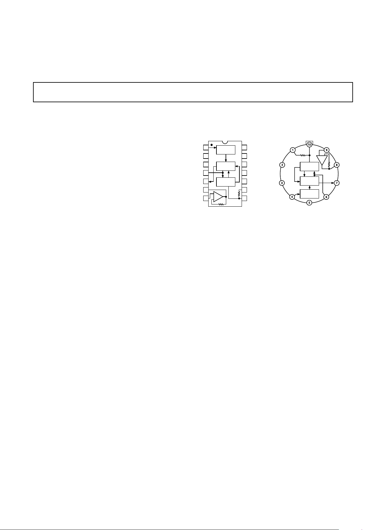
PIN CONNECTIONS &
FUNCTIONAL BLOCK DIAGRAM
is accurate within ±0.2 mV to ±0.3% of reading. Both versions
are specified for the 0°C to +70°C temperature range, and are
offered in either a hermetically sealed 14-pin DIP or a 10-lead
TO-100 metal can. Chips are also available.
PRODUCT HIGHLIGHTS
1. The AD636 computes the true root-mean-square of a complex ac (or ac plus dc) input signal and gives an equivalent dc
output level. The true rms value of a waveform is a more
useful quantity than the average rectified value since it is a
measure of the power in the signal. The rms value of an
ac-coupled signal is also its standard deviation.
2. The 200 millivolt full-scale range of the AD636 is compatible
with many popular display-oriented analog-to-digital converters. The low power supply current requirement permits
use in battery powered hand-held instruments.
3. The only external component required to perform measurements to the fully specified accuracy is the averaging capacitor. The value of this capacitor can be selected for the desired
trade-off of low frequency accuracy, ripple, and settling time.
4. The on-chip buffer amplifier can be used to buffer either the
input or the output. Used as an input buffer, it provides
accurate performance from standard 10 MΩ input attenua-
tors. As an output buffer, it can supply up to 5 milliamps of
output current.
5. The AD636 will operate over a wide range of power supply
voltages, including single +5 V to +24 V or split ±2.5 V to
±16.5 V sources. A standard 9 V battery will provide several
hundred hours of continuous operation.
One Technology Way, P.O. Box 9106, Norwood, MA 02062-9106, U.S.A.
Tel: 781/329-4700 World Wide Web Site: http://www.analog.com
Fax: 781/326-8703 © Analog Devices, Inc., 1999
V
IN
NC
–V
S
C
AV
dB
BUF OUT
BUF IN
+V
S
NC
NC
NC
COMMON
R
L
I
OUT
AD636
14
13
12
11
10
9
8
1
2
3
4
5
6
7
ABSOLUTE
VALUE
SQUARER
DIVIDER
BUF
SQUARER
DIVIDER
ABSOLUTE
VALUE
AD636
BUF OUT
dB
C
AV
BUF IN
R
L
COMMON
+V
S
V
IN
–V
S
I
OUT
CURRENT
MIRROR
+–
+
–
CURRENT
MIRROR
BUF
10kV
10kV
10kV
10kV
NC = NO CONNECT

AD636–SPECIFICATIONS
(@ +25ⴗC, and +VS = +3 V, –VS = –5 V, unless otherwise noted)
REV. B–2–
M
odel AD636J AD636K
Min Typ Max Min Typ Max Units
TRANSFER FUNCTION
V
OUT
= avg. ( V
IN
)
2
V
OUT
= avg. ( V
IN
)
2
CONVERSION ACCURACY
Total Error, Internal Trim
1, 2
ⴞ0.5 ⴞ1.0 ⴞ0.2 ⴞ0.5 mV ±% of Reading
vs. Temperature, 0°C to +70°C ±0.1 ±0.01 ±0.1 ±0.005 mV ±% of Reading/°C
vs. Supply Voltage ±0.1 ±0.01 ±0.1 ±0.01 mV ±% of Reading/V
dc Reversal Error at 200 mV ±0.2 ±0.1 % of Reading
Total Error, External Trim
1
±0.3 ±0.3 ±0.1 ±0.2 mV ±% of Reading
ERROR VS. CREST FACTOR
3
Crest Factor 1 to 2 Specified Accuracy Specified Accuracy
Crest Factor = 3 –0.2 –0.2 % of Reading
Crest Factor = 6 –0.5 –0.5 % of Reading
AVERAGING TIME CONSTANT 25 25 ms/µF CAV
INPUT CHARACTERISTICS
Signal Range, All Supplies
Continuous rms Level 0 to 200 0 to 200 mV rms
Peak Transient Inputs
+3 V, –5 V Supply ±2.8 ±2.8 V pk
±2.5 V Supply ±2.0 ±2.0 V pk
±5 V Supply ±5.0 ±5.0 V pk
Maximum Continuous Nondestructive
Input Level (All Supply Voltages) ±12 ±12 V pk
Input Resistance 5.33 6.67 8 5.33 6.67 8 kΩ
Input Offset Voltage ±0.5 ±0.2 mV
FREQUENCY RESPONSE
2, 4
Bandwidth for 1% Additional Error (0.09 dB)
V
IN
= 10 mV 14 14 kHz
V
IN
= 100 mV 90 90 kHz
V
IN
= 200 mV 130 130 kHz
±3 dB Bandwidth
V
IN
= 10 mV 100 100 kHz
V
IN
= 100 mV 900 900 kHz
VIN = 200 mV 1.5 1.5 MHz
OUTPUT CHARACTERISTICS
2
Offset Voltage, VIN = COM ⴞ0.5 ⴞ0.2 mV
vs. Temperature ±10 ±10 µV/°C
vs. Supply ±0.1 ±0.1 mV/ V
Voltage Swing
+3 V, –5 V Supply 0.3 0 to +1.0 0.3 0 to +1.0 V
±5 V to ±16.5 V Supply 0.3 0 to +1.0 0.3 0 to +1.0 V
Output Impedance 8 10 12 8 10 12 kΩ
dB OUTPUT
Error, V
IN
= 7 mV to 300 mV rms ±0.3 ⴞ0.5 ±0.1 ⴞ0.2 dB
Scale Factor –3.0 –3.0 mV/dB
Scale Factor Temperature Coefficient +0.33 +0.33 % of Reading/°C
–0.033 –0.033 dB/°C
I
REF
for 0 dB = 0.1 V rms 248 2 4 8 µA
I
REF
Range 1 50 1 50 µA
I
OUT
TERMINAL
I
OUT
Scale Factor 100 100 µA/V rms
I
OUT
Scale Factor Tolerance –20 ±10 +20 –20 ±10 +20 %
Output Resistance 8 10 12 8 10 12 kΩ
Voltage Compliance –V
S
to (+V
S
–VS to (+V
S
–2 V) –2 V) V
BUFFER AMPLIFIER
Input and Output Voltage Range –V
S
to (+V
S
–VS to (+V
S
–2 V) –2 V) V
Input Offset Voltage, R
S
= 10k ±0.8 ⴞ2 ±0.5 ⴞ1 mV
Input Bias Current 100 300 100 300 nA
Input Resistance 10
8
10
8
Ω
Output Current (+5 mA, (+5 mA,
–130 µA) –130 µA)
Short Circuit Current 20 20 mA
Small Signal Bandwidth l l MHz
Slew Rate
5
55V/µs
POWER SUPPLY
Voltage, Rated Performance +3, –5 +3, –5 V
Dual Supply +2, –2.5 ±16.5 +2, –2.5 ±16.5 V
Single Supply +5 +24 +5 +24 V
Quiescent Current
6
0.80 1.00 0.80 1.00 mA
ORDERING GUIDE
Temperature Package Package
Model Range Descriptions Options
AD636JD 0°C to +70°C Side Brazed Ceramic DIP D-14
AD636KD 0°C to +70°C Side Brazed Ceramic DIP D-14
AD636JH 0°C to +70°C Header H-10A
AD636KH 0°C to +70°C Header H-10A
AD636J Chip 0°C to +70°C Chip
AD636JD/+ 0°C to +70°C Side Brazed Ceramic DIP D-14
AD636
M
odel AD636J AD636K
Min Typ Max Min Typ Max Units
TEMPERATURE RANGE
Rated Performance 0 +70 0 +70 °C
Storage –55 +150 –55 +150 °C
TRANSISTOR COUNT 62 62
NOTES
1
Accuracy specified for 0 mV to 200 mV rms, dc or 1 kHz sine wave input. Accuracy is degraded at higher rms signal levels.
2
Measured at Pin 8 of DIP (I
OUT
), with Pin 9 tied to common.
3
Error vs. crest factor is specified as additional error for a 200 mV rms rectangular pulse trim, pulse width = 200 µs.
4
Input voltages are expressed in volts rms.
5
With 10 kΩ pull down resistor from Pin 6 (BUF OUT) to –V
S
.
6
With BUF input tied to Common.
Specifications subject to change without notice.
All min and max specifications are guaranteed. Specifications shown in boldface are tested on all production units at final electrical test and are used to calculate outgoing
quality levels.
ABSOLUTE MAXIMUM RATINGS
1
Supply Voltage
Dual Supply . . . . . . . . . . . . . . . . . . . . . . . . . . . . . . . ±16.5 V
Single Supply . . . . . . . . . . . . . . . . . . . . . . . . . . . . . . . +24 V
Internal Power Dissipation
2
. . . . . . . . . . . . . . . . . . . .500 mW
Maximum Input Voltage . . . . . . . . . . . . . . . . . . . . ±12 V Peak
Storage Temperature Range N, R . . . . . . . . . –55°C to +150°C
Operating Temperature Range
AD636J/K . . . . . . . . . . . . . . . . . . . . . . . . . . . 0°C to +70°C
Lead Temperature Range (Soldering 60 sec) . . . . . . . . +300°C
ESD Rating . . . . . . . . . . . . . . . . . . . . . . . . . . . . . . . . . . 1000 V
NOTES
1
Stresses above those listed under Absolute Maximum Ratings may cause perma-
nent damage to the device. This is a stress rating only; functional operation of the
device at these or any other conditions above those indicated in the operational
section of this specification is not implied. Exposure to absolute maximum rating
conditions for extended periods may affect device reliability.
2
10-Lead Header: θJA = 150°C/Watt.
14-Lead Side Brazed Ceramic DIP: θJA = 95°C/Watt.
METALIZATION PHOTOGRAPH
Contact factory for latest dimensions.
Dimensions shown in inches and (mm).
COM
10
R
L
9
+V
S
14
1a*
1b*
V
IN
3
–V
S
4
C
AV
5
dB
7 BUF IN
6 BUF OUT
8 I
OUT
0.1315 (3.340)
0.0807
(2.050)
PAD NUMBERS CORRESPOND TO PIN NUMBERS
FOR THE TO-116 14-PIN CERAMIC DIP PACKAGE.
NOTE
*BOTH PADS SHOWN MUST BE CONNECTED TO V
IN
.
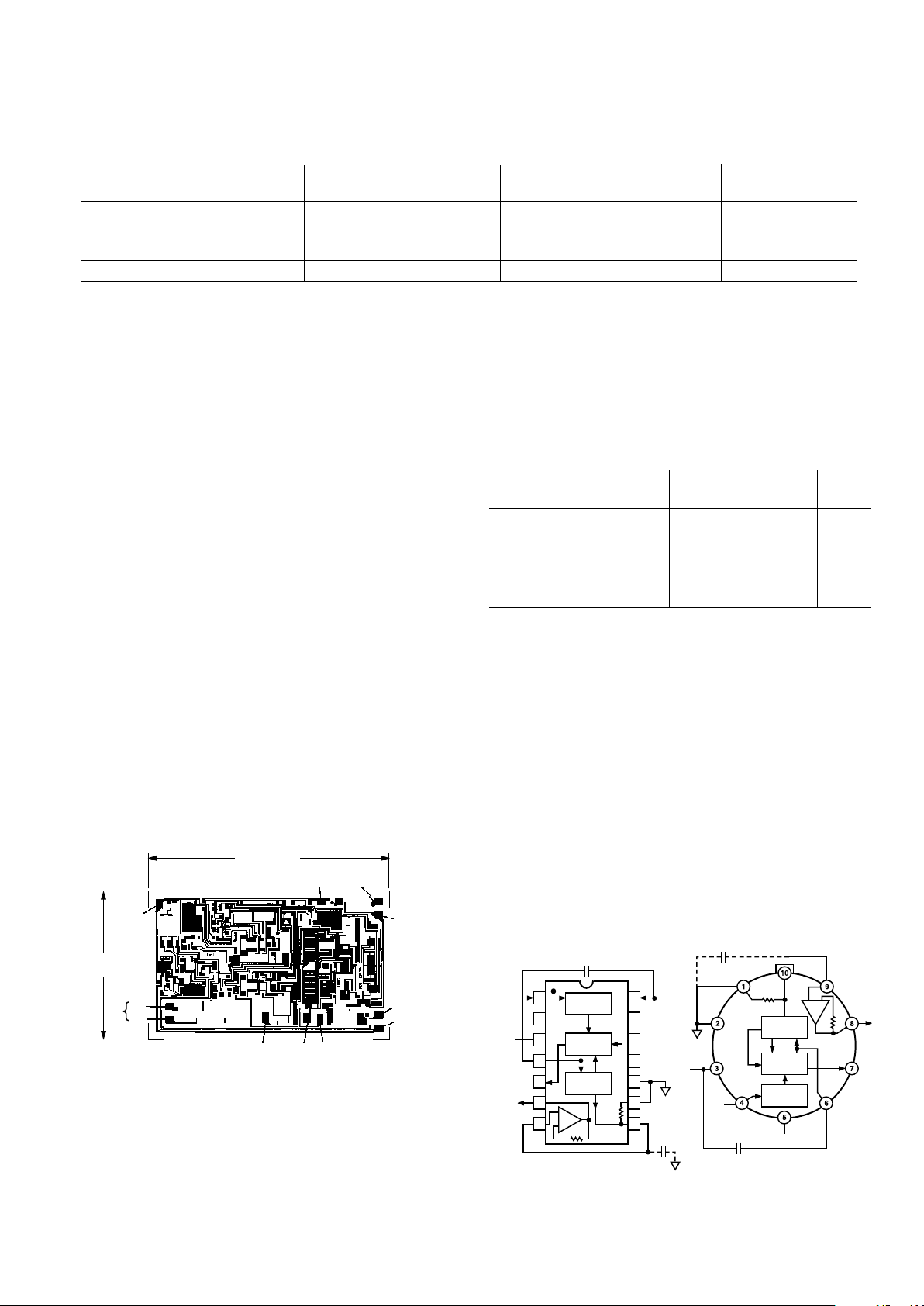
STANDARD CONNECTION
The AD636 is simple to connect for the majority of high accuracy rms measurements, requiring only an external capacitor to
set the averaging time constant. The standard connection is
shown in Figure 1. In this configuration, the AD636 will measure the rms of the ac and dc level present at the input, but will
show an error for low frequency inputs as a function of the filter
capacitor, C
AV
, as shown in Figure 5. Thus, if a 4 µF capacitor
is used, the additional average error at 10 Hz will be 0.1%, at
3 Hz it will be 1%. The accuracy at higher frequencies will be
according to specification. If it is desired to reject the dc input, a
capacitor is added in series with the input, as shown in Figure 3; the capacitor must be nonpolar. If the AD636 is driven
with power supplies with a considerable amount of high frequency
ripple, it is advisable to bypass both supplies to ground with
0.1 µF ceramic discs as near the device as possible. C
F
is an
optional output ripple filter, as discussed elsewhere in this data
sheet.
AD636
14
13
12
11
10
9
8
1
2
3
4
5
6
7
ABSOLUTE
VALUE
SQUARER
DIVIDER
BUF
+
–
CURRENT
MIRROR
10kV
10kV
V
IN
–V
S
+V
S
V
OUT
C
F
(OPTIONAL)
+–
C
AV
SQUARER
DIVIDER
ABSOLUTE
VALUE
AD636
CURRENT
MIRROR
+–
BUF
10kV
10kV
+V
S
V
IN
–V
S
+–
C
AV
V
OUT
C
F
(OPTIONAL)
Figure 1. Standard RMS Connection
REV. B –3–

AD636
REV. B–4–
flows into Pin 10 (Pin 2 on the “H” package). Alternately, the
COM pin of some CMOS ADCs provides a suitable artificial
ground for the AD636. AC input coupling requires only capacitor C2 as shown; a dc return is not necessary as it is provided
internally. C2 is selected for the proper low frequency break
point with the input resistance of 6.7 kΩ; for a cut-off at 10 Hz,
C2 should be 3.3 µF. The signal ranges in this connection are
slightly more restricted than in the dual supply connection. The
load resistor, R
L
, is necessary to provide current sinking capability.
1
2
3
4
5
6
7
AD636
14
13
12
11
10
9
8
ABSOLUTE
VALUE
SQUARER
DIVIDER
10kV
10kV
CURRENT
MIRROR
V
IN
V
OUT
+V
S
–+
C
AV
20kV
C2
3.3mF
NONPOLARIZED
R
L
10kV to 1kV
39kV
0.1mF
0.1mF
+
–
BUF
Figure 3. Single Supply Connection
CHOOSING THE AVERAGING TIME CONSTANT
The AD636 will compute the rms of both ac and dc signals. If
the input is a slowly-varying dc voltage, the output of the AD636
will track the input exactly. At higher frequencies, the average
output of the AD636 will approach the rms value of the input
signal. The actual output of the AD636 will differ from the ideal
output by a dc (or average) error and some amount of ripple, as
demonstrated in Figure 4.
DOUBLE-FREQUENCY
RIPPLE
E
O
IDEAL
E
O
AVERAGE EO = E
O
DC ERROR = EO – EO (IDEAL)
TIME
Figure 4. Typical Output Waveform for Sinusoidal Input
The dc error is dependent on the input signal frequency and the
value of C
AV
. Figure 5 can be used to determine the minimum
value of C
AV
which will yield a given % dc error above a given
frequency using the standard rms connection.
The ac component of the output signal is the ripple. There are
two ways to reduce the ripple. The first method involves using
a large value of C
AV
. Since the ripple is inversely proportional
to C
AV
, a tenfold increase in this capacitance will effect a tenfold
reduction in ripple. When measuring waveforms with high crest
factors, (such as low duty cycle pulse trains), the averaging time
constant should be at least ten times the signal period. For
example, a 100 Hz pulse rate requires a 100 ms time constant,
which corresponds to a 4 µF capacitor (time constant = 25 ms
per µF).
APPLYING THE AD636
The input and output signal ranges are a function of the supply
voltages as detailed in the specifications. The AD636 can also
be used in an unbuffered voltage output mode by disconnecting
the input to the buffer. The output then appears unbuffered
across the 10 kΩ resistor. The buffer amplifier can then be used
for other purposes. Further, the AD636 can be used in a current
output mode by disconnecting the 10 kΩ resistor from the
ground. The output current is available at Pin 8 (Pin 10 on the
“H” package) with a nominal scale of 100 µA per volt rms input,
positive out.
OPTIONAL TRIMS FOR HIGH ACCURACY
If it is desired to improve the accuracy of the AD636, the external trims shown in Figure 2 can be added. R4 is used to trim the
offset. The scale factor is trimmed by using R1 as shown. The
insertion of R2 allows R1 to either increase or decrease the scale
factor by ±1.5%.
The trimming procedure is as follows:
1. Ground the input signal, V
IN
, and adjust R4 to give zero
volts output from Pin 6. Alternatively, R4 can be adjusted to
give the correct output with the lowest expected value of V
IN.
2. Connect the desired full-scale input level to VIN, either dc or
a calibrated ac signal (1 kHz is the optimum frequency);
then trim R1 to give the correct output from Pin 6, i.e.,
200 mV dc input should give 200 mV dc output. Of course,
a ±200 mV peak-to-peak sine wave should give a 141.4 mV
dc output. The remaining errors, as given in the specifications, are due to the nonlinearity.
1
2
3
4
5
6
7
AD636
14
13
12
11
10
9
8
ABSOLUTE
VALUE
SQUARER
DIVIDER
10kV
10kV
CURRENT
MIRROR
V
IN
V
OUT
+V
S
–V
S
SCALE
FACTOR
ADJUST
R1
200V
61.5%
–+
C
AV
+V
S
–V
S
R4
500kV
OFFSET
ADJUST
R3
470kV
R2
154V
+
–
BUF
Figure 2. Optional External Gain and Output Offset Trims
SINGLE SUPPLY CONNECTION
The applications in Figures 1 and 2 assume the use of dual
power supplies. The AD636 can also be used with only a single
positive supply down to +5 volts, as shown in Figure 3. Figure 3
is optimized for use with a 9 volt battery. The major limitation
of this connection is that only ac signals can be measured since
the input stage must be biased off ground for proper operation.
This biasing is done at Pin 10; thus it is critical that no extraneous signals be coupled into this point. Biasing can be accomplished by using a resistive divider between +V
S
and ground.
The values of the resistors can be increased in the interest of
lowered power consumption, since only 1 microamp of current

AD636
REV. B –5–
INPUT FREQUENCY – Hz
100
0.01
1 100k
REQUIRED C
AV
– mF
1.0
10 100 1k 10k
10
0.1
1.0
10
100
0.1
0.01
FOR 1% SETTLING TIME IN SECONDS
MULTIPLY READING BY 0.115
0.01% ERROR
0.1% ERROR
VALUES FOR CAV AND
1% SETTLING TIME FOR
STATED % OF READING
AVERAGING ERROR*
ACCURACY 620% DUE TO
COMPONENT TOLERANCE
10% ERROR
*% dc ERROR + % RIPPLE (PEAK)
1% ERROR
Figure 5. Error/Settling Time Graph for Use with the
Standard rms Connection
The primary disadvantage in using a large CAV to remove ripple
is that the settling time for a step change in input level is increased proportionately. Figure 5 shows the relationship between C
AV
and 1% settling time is 115 milliseconds for each
microfarad of C
AV
. The settling time is twice as great for decreasing signals as for increasing signals (the values in Figure 5
are for decreasing signals). Settling time also increases for low
signal levels, as shown in Figure 6.
rms INPUT LEVEL
10.0
7.5
0
1mV 1V10mV
SETTLING TIME RELATIVE TO
SETTLING TIME @ 200mV rms
100mV
1.0
5.0
2.5
Figure 6. Settling Time vs. Input Level
A better method for reducing output ripple is the use of a
“post-filter.” Figure 7 shows a suggested circuit. If a single pole
filter is used (C3 removed, R
X
shorted), and C2 is approxi-
mately 5 times the value of C
AV
, the ripple is reduced as shown
in Figure 8, and settling time is increased. For example, with
C
AV
= 1 µF and C2 = 4.7 µF, the ripple for a 60 Hz input is re-
duced from 10% of reading to approximately 0.3% of reading.
The settling time, however, is increased by approximately a
factor of 3. The values of C
AV
and C2 can therefore be reduced
to permit faster settling times while still providing substantial
ripple reduction.
The two-pole post-filter uses an active filter stage to provide
even greater ripple reduction without substantially increasing
the settling times over a circuit with a one-pole filter. The values
of C
AV
, C2, and C3 can then be reduced to allow extremely fast
settling times for a constant amount of ripple. Caution should
be exercised in choosing the value of C
AV
, since the dc error is
dependent upon this value and is independent of the post filter.
For a more detailed explanation of these topics refer to the
RMS-to-DC Conversion Application Guide, 2nd Edition, available
from Analog Devices.
1
2
3
4
5
6
7
AD636
14
13
12
11
10
9
8
ABSOLUTE
VALUE
SQUARER
DIVIDER
+
–
BUF
10kV
10kV
CURRENT
MIRROR
V
rms
OUT
+V
S
V
IN
–V
S
C
AV
+
–
+
–
+
–
C2
C3
(FOR SINGLE POLE, SHORT Rx,
REMOVE C3)
Rx
10kV
Figure 7. 2 Pole ‘’Post’’ Filter
FREQUENCY – Hz
10
0.1
10 10k
DC ERROR OR RIPPLE – % of Reading
1
1k100
p-p RIPPLE
CAV = 1mF (FIG 1)
p-p RIPPLE
(ONE POLE)
CAV = 1mF
C2 = 4.7mF
DC ERROR
CAV = 1mF
(ALL FILTERS)
p-p RIPPLE
(TWO POLE)
CAV = 1mF, C2 = C3 = 4.7mF
Figure 8. Performance Features of Various Filter Types
RMS MEASUREMENTS
AD636 PRINCIPLE OF OPERATION
The AD636 embodies an implicit solution of the rms equation
that overcomes the dynamic range as well as other limitations
inherent in a straightforward computation of rms. The actual
computation performed by the AD636 follows the equation:
V rms = Avg .
V
IN
2
V rms
Figure 9 is a simplified schematic of the AD636; it is subdivided
into four major sections: absolute value circuit (active rectifier),
squarer/divider, current mirror, and buffer amplifier. The input
voltage, V
IN
, which can be ac or dc, is converted to a unipolar
current I
1
, by the active rectifier A1, A2. I1 drives one input of
the squarer/divider, which has the transfer function:
I
4
=
I
1
2
I
3
The output current, I4, of the squarer/divider drives the current
mirror through a low-pass filter formed by R1 and the externally
connected capacitor, C
AV
. If the R1, CAV time constant is much
greater than the longest period of the input signal, then I
4
is
effectively averaged. The current mirror returns a current I
3
,
which equals Avg. [I
4
], back to the squarer/divider to complete
the implicit rms computation. Thus:
I
4
= Avg .
I
1
2
I
4
= I
1
rms

AD636
REV. B–6–
Addition of an external resistor in parallel with RE alters this
voltage divider such that increased negative swing is possible.
Figure 11 shows the value of R
EXTERNAL
for a particular ratio of
V
PEAK
to –VS for several values of R
LOAD.
Addition, of R
EXTERNAL
increases the quiescent current of the buffer amplifier by an
amount equal to R
EXT
/–VS. Nominal buffer quiescent current
with no R
EXTERNAL
is 30 µA at –V
S
= –5 V.
R
EXTERNAL
– V
1.0
0.5
0
01M1k
RATIO OF V
PEAK
/V
SUPPLY
10k 100k
RL = 6.7kV
RL = 16.7kV
RL = 50kV
Figure 11. Ratio of Peak Negative Swing to –VS vs.
R
EXTERNAL
for Several/Load Resistances
FREQUENCY RESPONSE
The AD636 utilizes a logarithmic circuit in performing the
implicit rms computation. As with any log circuit, bandwidth is
proportional to signal level. The solid lines in the graph below
represent the frequency response of the AD636 at input levels
from 1 millivolt to 1 volt rms. The dashed lines indicate the
upper frequency limits for 1%, 10%, and ±3 dB of reading
additional error. For example, note that a 1 volt rms signal will
produce less than 1% of reading additional error up to 220 kHz.
A 10 millivolt signal can be measured with 1% of reading addi-
tional error (100 µV) up to 14 kHz.
FREQUENCY – Hz
1
V
OUT
– Volts
200m
100m
10m
1m
30m
1k 10k 100k 1M
100m
1 VOLT rms INPUT
200mV rms INPUT
100mV rms INPUT
30mV rms INPUT
10mV rms
INPUT
1mV rms INPUT
10% 63dB
10M
1%
Figure 12. AD636 Frequency Response
AC MEASUREMENT ACCURACY AND CREST FACTOR
Crest factor is often overlooked in determining the accuracy of
an ac measurement. Crest factor is defined as the ratio of the
peak signal amplitude to the rms value of the signal (C.F. = V
P
/
V rms) Most common waveforms, such as sine and triangle
waves, have relatively low crest factors (<2). Waveforms that
The current mirror also produces the output current, I
OUT
,
which equals 2I
4
. I
OUT
can be used directly or converted to a
voltage with R2 and buffered by A
4
to provide a low impedance
voltage output. The transfer function of the AD636 thus results:
V
OUT
= 2 R2 I rms =V
IN
rms
The dB output is derived from the emitter of Q3, since the voltage at this point is proportional to –log V
IN
. Emitter follower,
Q
5
, buffers and level shifts this voltage, so that the dB output
voltage is zero when the externally supplied emitter current
(I
REF
) to Q5 approximates I3.
A4 6
7
5
3
984
10
14
A1
A2
A3
1
+V
S
COM
R
L
dB
OUT
BUF
OUT
BUFFER
BUF
IN
10k
V
Q5
Q4Q2
Q1
Q3
ONE-QUADRANT
SQUARER/
DIVIDER
C
AVIOUT
ABSOLUTE VALUE/
VOLTAGE–CURRENT
CONVERTER
V
IN
R3
10kV
8kV
8kV
+
R4
20kV
|VIN|
R4
I
1
10mA
FS
I
3
20mA
FS
R1
25kV
I
4
R2
10kV
I
REF
–V
S
CURRENT MIRROR
Figure 9. Simplified Schematic
THE AD636 BUFFER AMPLIFIER
The buffer amplifier included in the AD636 offers the user
additional application flexibility. It is important to understand
some of the characteristics of this amplifier to obtain optimum
performance. Figure 10 shows a simplified schematic of the buffer.
Since the output of an rms-to-dc converter is always positive, it
is not necessary to use a traditional complementary Class AB
output stage. In the AD636 buffer, a Class A emitter follower is
used instead. In addition to excellent positive output voltage
swing, this configuration allows the output to swing fully down
to ground in single-supply applications without the problems
associated with most IC operational amplifiers.
CURRENT
MIRROR
BUFFER
INPUT
BUFFER
OUTPUT
+V
S
R
E
40kV
10kV
R
EXTERNAL
PTI
NAL EE TEXT
–V
S
R
LOAD
5mA5mA
Figure 10. AD636 Buffer Amplifier Simplified Schematic
When this amplifier is used in dual-supply applications as an
input buffer amplifier driving a load resistance referred to
ground, steps must be taken to insure an adequate negative
voltage swing. For negative outputs, current will flow from the
load resistor through the 40 kΩ emitter resistor, setting up a
voltage divider between –V
S
and ground. This reduced effective
–V
S
, will limit the available negative output swing of the buffer.

AD636
REV. B –7–
Circuit Description
The input voltage, VIN, is ac coupled by C4 while resistor R8,
together with diodes D1, and D2, provide high input voltage
protection.
The buffer’s output, Pin 6, is ac coupled to the rms converter’s
input (Pin 1) by capacitor C2. Resistor, R9, is connected between
the buffer’s output, a Class A output stage, and the negative output
swing. Resistor R1, is the amplifier’s “bootstrapping” resistor.
With this circuit, single supply operation is made possible by
setting “ground” at a point between the positive and negative
sides of the battery. This is accomplished by sending 250 µA
from the positive battery terminal through resistor R2, then
through the 1.2 volt AD589 bandgap reference, and finally back
to the negative side of the battery via resistor R10. This sets
ground at 1.2 volts +3.18 volts (250 µA × 12.7 kΩ) = 4.4 volts
below the positive battery terminal and 5.0 volts (250 µA × 20 kΩ)
above the negative battery terminal. Bypass capacitors C3 and
C5 keep both sides of the battery at a low ac impedance to
ground. The AD589 bandgap reference establishes the 1.2 volt
regulated reference voltage which together with resistor R3 and
trimming potentiometer R4 set the zero dB reference current I
REF
.
Performance Data
0 dB Reference Range = 0 dBm (770 mV) to –20 dBm
(77 mV) rms
0 dBm = 1 milliwatt in 600 Ω
Input Range (at I
REF
= 770 mV) = 50 dBm
Input Impedance = approximately 10
10
Ω
V
SUPPLY
Operating Range +5 V dc to +20 V dc
I
QUIESCENT
= 1. 8 mA typical
Accuracy with 1 kHz sine wave and 9 volt dc supply:
0 dB to –40 dBm ± 0.1 dBm
0 dBm to –50 dBm ± 0.15 dBm
+10 dBm to –50 dBm ± 0.5 dBm
Frequency Response ⴞ3 dBm
Input
0 dBm = 5 Hz to 380 kHz
–10 dBm = 5 Hz to 370 kHz
–20 dBm = 5 Hz to 240 kHz
–30 dBm = 5 Hz to 100 kHz
–40 dBm = 5 Hz to 45 kHz
–50 dBm = 5 Hz to 17 kHz
Calibration
1. First calibrate the zero dB reference level by applying a 1 kHz
sine wave from an audio oscillator at the desired zero dB
amplitude. This may be anywhere from zero dBm (770 mV
rms – 2.2 volts p-p) to –20 dBm (77 mV rms 220 mV – p-p).
Adjust the I
REF
cal trimmer for a zero indication on the analog
meter.
2. The final step is to calibrate the meter scale factor or gain.
Apply an input signal –40 dB below the set zero dB reference
and adjust the scale factor calibration trimmer for a 40 µA
reading on the analog meter.
The temperature compensation resistors for this circuit may be
purchased from: Tel Labs Inc., 154 Harvey Road, P.O. Box 375,
Londonderry, NH 03053, Part #Q332A 2 kΩ 1% +3500 ppm/°C
or from Precision Resistor Company, 109 U.S. Highway 22, Hill-
side, NJ 07205, Part #PT146 2 kΩ 1% +3500 ppm/°C.
resemble low duty cycle pulse trains, such as those occurring in
switching power supplies and SCR circuits, have high crest
factors. For example, a rectangular pulse train with a 1% duty
cycle has a crest factor of 10 (C.F. =
1 η
).
Figure 13 is a curve of reading error for the AD636 for a 200 mV
rms input signal with crest factors from 1 to 7. A rectangular
pulse train (pulse width 200 µs) was used for this test since it is
the worst-case waveform for rms measurement (all the energy is
contained in the peaks). The duty cycle and peak amplitude
were varied to produce crest factors from 1 to 7 while maintaining a constant 200 mV rms input amplitude.
CREST FACTOR
0.5
0
–1.0
172
INCREASE IN ERROR – % of Reading
3456
–0.5
T
V
P
0
200ms
E
O
h = DUTY CYCLE =
CF = 1/ h
E
IN
(rms) = 200mV
200ms
T
Figure 13. Error vs. Crest Factor
A COMPLETE AC DIGITAL VOLTMETER
Figure 14 shows a design for a complete low power ac digital
voltmeter circuit based on the AD636. The 10 MΩ input
attenuator allows full-scale ranges of 200 mV, 2 V, 20 V and
200 V rms. Signals are capacitively coupled to the AD636 buffer
amplifier, which is connected in an ac bootstrapped configura-
tion to minimize loading. The buffer then drives the 6.7 kΩ
input impedance of the AD636. The COM terminal of the ADC
chip provides the false ground required by the AD636 for single
supply operation. An AD589 1.2 volt reference diode is used to
provide a stable 100 millivolt reference for the ADC in the linear rms mode; in the dB mode, a 1N4148 diode is inserted in
series to provide correction for the temperature coefficient of the
dB scale factor. Calibration of the meter is done by first adjusting offset pot R17 for a proper zero reading, then adjusting the
R13 for an accurate readout at full scale.
Calibration of the dB range is accomplished by adjusting R9 for
the desired 0 dB reference point, then adjusting R14 for the
desired dB scale factor (a scale of 10 counts per dB is convenient).
Total power supply current for this circuit is typically 2.8 mA
using a 7106-type ADC.
A LOW POWER, HIGH INPUT IMPEDANCE dB METER
Introduction
The portable dB meter circuit featured here combines the functions of the AD636 rms converter, the AD589 voltage reference,
and a µA776 low power operational amplifier. This meter offers
excellent bandwidth and superior high and low level accuracy
while consuming minimal power from a standard 9 volt transistor radio battery.
In this circuit, the built-in buffer amplifier of the AD636 is used
as a “bootstrapped” input stage increasing the normal 6.7 kΩ
input Z to an input impedance of approximately 10
10
Ω.

AD636
REV. B–8–
C651d–0–8/99
PRINTED IN U.S.A.
1
2
3
4
5
6
7
AD636
14
13
12
11
10
9
8
ABSOLUTE
VALUE
SQUARER
DIVIDER
+
–
BUF
10kV
10kV
CURRENT
MIRROR
+
–
+
–
+
+V
S
3-1/2
DIGIT
LCD
DISPLAY
3-1/2 DIGIT
7106 TYPE
A/D
CONVERTER
+V
DD
REF HI
REF LO
COM
HI
LO
–V
SS
ANALOG
IN
+
–
+
+V
DD
ON
OFF
1mF
9V
BATTERY
–V
SS
LXD 7543
–V
S
C6
0.01mF
R15
1MV
LIN
dB
LIN
dB
LIN
SCALE
R13
500V
R12
1kV
R11
10kV
D2
1N4148
LIN
dB
R14
10kV
dB
SCALE
D3
1.2V
AD589
R10
20kV
R9
100kV
0dB SET
R8
2.49kV
C7
6.8mF
C4
2.2mF
D1
1N4148
R6
1MV
R5
47kV
1W
10%
C3
0.02mF
200mV
V
IN
R1
9MV
2V
R2
900kV
20V
R3
90kV
200V
R4
10kV
COM
6.8mF
R7
20kV
D4
1N4148
Figure 14. A Portable, High Z Input, RMS DPM and dB Meter Circuit
1
2
3
4
5
6
7
AD636
14
13
12
11
10
9
8
ABSOLUTE
VALUE
SQUARER
DIVIDER
BUF
+
–
10kV
10kV
CURRENT
MIRROR
+–
+
–
mA776
+–
+
+
+
+
ON/OFF
9 VOLT
SCALE FACTOR
ADJUST
R5
10kV
0–50mA
R11
820kV
5%
100mA
R4
500kV
I
REF
ADJUST
R3
5kV
+1.2 VOLTS
AD589J
250mA
+
R6
100V
*R7
2kV
C6
0.1mF
+4.4 VOLTS
R2
12.7kV
C3
10mF
C5
10mF
R10
20kV
+4.7 VOLTS
C1
3.3mF
C2
6.8mF
R1
1MV
D1
1N6263
SIGNAL
INPUT
C4
0.1mF
R8
47kV
1 WATT
D2
1N6263
R9
10kV
ALL RESISTORS 1/4 WATT 1% METAL FILM UNLESS OTHERWISE STATED EXCEPT
*WHICH IS 2kV +3500ppm 1% TC RESISTOR.
Figure 15. A Low Power, High Input Impedance dB Meter
OUTLINE DIMENSIONS
Dimensions shown in inches and (mm).
D Package (TO-116) H Package (TO-100)
14
1
7
8
0.098 (2.49) MAX
0.310 (7.87)
0.220 (5.59)
0.005 (0.13) MIN
PIN 1
0.100
(2.54)
BSC
SEATING
PLANE
0.023 (0.58)
0.014 (0.36)
0.060 (1.52)
0.015 (0.38)
0.200 (5.08)
MAX
0.200 (5.08)
0.125 (3.18)
0.070 (1.78)
0.030 (0.76)
0.150
(3.81)
MAX
0.785 (19.94) MAX
0.320 (8.13)
0.290 (7.37)
0.015 (0.38)
0.008 (0.20)
0.250 (6. 35) MIN
0.750 (19.05)
0.500 (12.70)
0.185 (4.70)
0.165 (4.19)
REFERENCE PLANE
0.050 (1.27) MAX
0.019 (0.48)
0.016 (0.41)
0.021 (0.53)
0.016 (0.41)
0.045 (1.14)
0.010 (0.25)
0.040 (1.02) MAX
BASE & SEATING PLANE
0.335 (8.51)
0.305 (7.75)
0.370 (9.40)
0.335 (8.51)
1
0.034 (0.86)
0.027 (0.69)
0.045 (1.14)
0.027 (0.69)
0.160 (4.06)
0.110 (2.79)
6
2
8
7
5
4
3
0.115
(2.92)
BSC
9
10
0.230 (5.84)
BSC
36° BSC
 Loading...