

www.BDTIC.com/ADI
Low Level, True RMS-to-DC Converter
FEATURES
True rms-to-dc conversion
200 mV full scale
Laser-trimmed to high accuracy
0.5% maximum error (AD636K)
1.0% maximum error (AD636J)
Wide response capability
Computes rms of ac and dc signals
1 MHz, −3 dB bandwidth: V rms > 100 mV
Signal crest factor of 6 for 0.5% error
dB output with 50 dB range
Low power: 800 μA quiescent current
Single or dual supply operation
Monolithic integrated circuit
Low cost
GENERAL DESCRIPTION
The AD636 is a low power monolithic IC that performs true
rms-to-dc conversion on low level signals. It offers performance
that is comparable or superior to that of hybrid and modular
converters costing much more. The AD636 is specified for a
signal range of 0 mV to 200 mV rms. Crest factors up to 6 can
be accommodated with less than 0.5% additional error, allowing
accurate measurement of complex input waveforms.
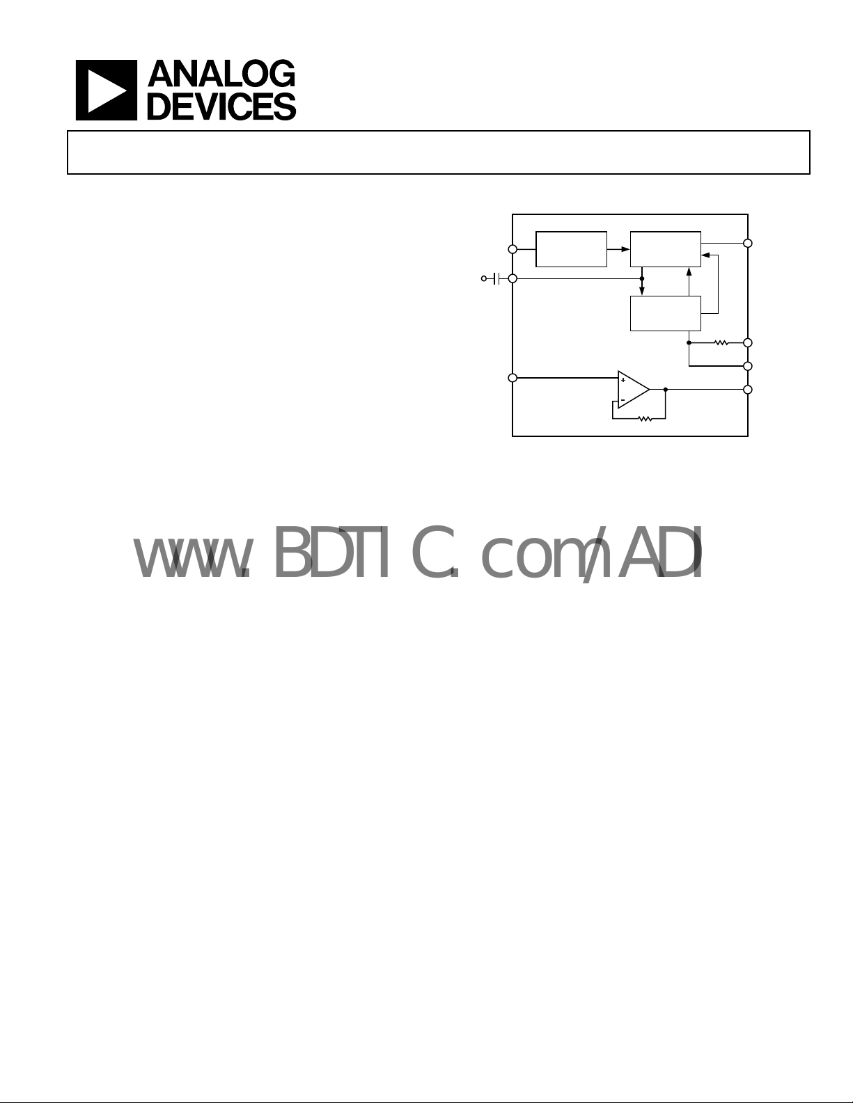
AD636
FUNCTIONAL BLOCK DIAGRAM
dB
R
L
I
OUT
BUF OUT
10kΩ
Figure 1.
SQUARER
DIVIDER
CURRENT
MIRROR
10kΩ
+V
S
BUF IN
V
IN
C
AV
ABSOLUTE
VALUE
AD636
at 200 mV rms. Therefore, no external trims are required to
achieve full-rated accuracy.
The AD636 is available in two accuracy grades. The total error
o
f the J-version is typically less than ±0.5 mV ± 1.0% of reading,
while the total error of the AD636K is less than ±0.2 mV to
±0.5% of reading. Both versions are temperature rated for
operation between 0°C and 70°C and available in 14-lead
SBDIP and 10-lead TO-100 metal can.
00787-001
The low power supply current requirement of the AD636,
ically 800 A, is ideal for battery-powered portable
typ
instruments. It operates from a wide range of dual and single
power supplies, from ±2.5 V to ±16.5 V or from +5 V to +24 V.
The input and output terminals are fully protected; the input
signal can exceed the power supply with no damage to the device
(allowing the presence of input signals in the absence of supply
voltage), and the output buffer amplifier is short-circuit protected.
The AD636 includes an auxiliary dB output derived from an
in
ternal circuit point that represents the logarithm of the rms
output. The 0 dB reference level is set by an externally supplied
current and can be selected to correspond to any input level from
0 dBm (774.6 mV) to −20 dBm (77.46 mV). Frequency response
ranges from 1.2 MHz at 0 dBm to greater than 10 kHz at −50 dBm.
The AD636 is easy to use. The device is factory-trimmed at the
wa
fer level for input and output offset, positive and negative
waveform symmetry (dc reversal error), and full-scale accuracy
Rev. D
Information furnished by Analog Devices is believed to be accurate and reliable. However, no
responsibility is assumed by Anal og Devices for its use, nor for any infringements of patents or ot her
rights of third parties that may result from its use. Specifications subject to change without notice. No
license is granted by implication or otherwise under any patent or patent rights of Analog Devices.
Trademarks and registered trademarks are the property of their respective owners.
The AD636 computes the true root-mean-square of a complex
ac (o
r ac plus dc) input signal and gives an equivalent dc output
level. The true rms value of a waveform is a more useful
quantity than the average rectified value because it is a measure
of the power in the signal. The rms value of an ac-coupled
signal is also its standard deviation.
The 200 mV full-scale range of the AD636 is compatible with
ma
ny popular display-oriented ADCs. The low power supply
current requirement permits use in battery-powered hand-held
instruments. An averaging capacitor is the only external
component required to perform measurements to the fully
specified accuracy is. Its value optimizes the trade-off between
low frequency accuracy, ripple, and settling time.
An optional on-chip amplifier acts as a buffer for the input or
e output signals. Used in the input, it provides accurate
th
performance from standard 10 M input attenuators. As an
output buffer, it sources up to 5 mA.
One Technology Way, P.O. Box 9106, Norwood, MA 02062-9106, U.S.A.
Tel: 781.329.4700 www.analog.com
Fax: 781.461.3113 ©2006 Analog Devices, Inc. All rights reserved.

AD636
www.BDTIC.com/ADI
TABLE OF CONTENTS
Features.............................................................................................. 1
AD636 Principle of Operation................................................9
Functional Block Diagram ..............................................................1
General Description......................................................................... 1
Revision History ...............................................................................2
Specifications..................................................................................... 3
Absolute Maximum Ratings............................................................ 5
ESD Caution.................................................................................. 5
Pin Configurations and Function Descriptions........................... 6
Applying the AD636......................................................................... 7
Standard Connection................................................................... 7
Optional Trims for High Accuracy............................................ 7
Single-Supply Connection........................................................... 7
Choosing the Averaging Time Constant................................... 8
RMS Measurements..................................................................... 9
REVISION HISTORY
The AD636 Buffer Amplifier.......................................................9
Frequency Response .................................................................. 10
AC Measurement Accuracy and Crest Factor (CF)............... 10
A Complete AC Digital Voltmeter........................................... 11
A Low Power, High Input, Impedance dB Meter....................... 11
Circuit Description................................................................ 11
Performance Data .................................................................. 11
Frequency Response ±3 dBm............................................... 11
Calibration .............................................................................. 11
Outline Dimensions....................................................................... 13
Ordering Guide .......................................................................... 13
11/06—Rev. C to Rev. D
Changes to General Description .................................................... 1
Changes to Table 1............................................................................ 3
Changes to Ordering Guide.......................................................... 13
1/06—Rev B to Rev. C
pdated Format..................................................................Universal
U
Changes to Figure 1 and General Description ............................. 1
Deleted Metalization Photograph.................................................. 3
Added Pin Configuration and Function Description Section.... 6
Updated Outline Dimensions....................................................... 14
Changes to Ordering Guide.......................................................... 14
8/99—Rev A to Rev. B
Rev. D | Page 2 of 16

AD636
(
www.BDTIC.com/ADI
SPECIFICATIONS
@ 25°C, +VS = +3 V, and −VS = –5 V, unless otherwise noted.
Table 1.
Model
TRANSFER FUNCTION
CONVERSION ACCURACY
Total Error, Internal Trim
vs. Temperature, 0°C to +70°C ±0.1 ± 0.01 ±0.1 ± 0.005
vs. Supply Voltage ±0.1 ± 0.01 ±0.1 ± 0.01
DC Reversal Error at 200 mV ±0.2 ±0.1 % of reading
Total Error, External Trim2 ±0.3 ± 0.3 ± 0.1 ± 0.2
ERROR VS. CREST FACTOR4
Crest Factor 1 to 2 Specified Accuracy Specified Accuracy
Crest Factor = 3 −0.2 −0.2 % of reading
Crest Factor = 6 −0.5 −0.5 % of reading
AVERAGING TIME CONSTANT 25 25 ms/F of CAV
INPUT CHARACTERISTICS
Signal Range, All Supplies
Continuous RMS Level 0 to 200 0 to 200 mV rms
Peak Transient Inputs
+3 V, −5 V Supply ±2.8 ±2.8 V p-p
±2.5 V Supply ±2.0 ±2.0 V p-p
±5 V Supply ±5.0 ±5.0 V p-p
Maximum Continuous
Nondestructive
Input Level (All Supply Voltages) ±12 ±12 V p-p
Input Resistance 5.33 6.67 8 5.33 6.67 8 kΩ
Input Offset Voltage ±0.5 ±0.2 mV
FREQUENCY RESPONSE
Bandwidth for 1% Additional
Error (0.09 dB)
VIN = 10 mV 14 14 kHz
VIN = 100 mV 90 90 kHz
VIN = 200 mV 130 130 kHz
±3 dB Bandwidth
VIN = 10 mV 100 100 kHz
VIN = 100 mV 900 900 kHz
VIN = 200 mV 1.5 1.5 MHz
OUTPUT CHARACTERISTICS3
Offset Voltage, VIN = COM
vs. Temperature ±10 ±10 V/°C
vs. Supply ±0.1 ±0.1 mV/V
Voltage Swing
+3 V, −5 V Supply 0.3 0 to 1.0 0.3 0 to 1.0 V
±5 V to ±16.5 V Supply 0.3 0 to 1.0 0.3 0 to 1.0 V
Output Impedance 8 10 12 8 10 12 kΩ
2, 3
3, 5
Min Typ Max Min Typ Max
OUT
1
AD636J AD636K
Unit
2
)
VavgV ×=
IN
±0.5 ± 1.0
±0.5
2
()
OUT
VavgV ×=
IN
±0.2 ± 0.5
±0.2
mV ± % of
ading
re
mV ± % of
ading/°C
re
mV ± % of
ading/V
re
mV ± % of
ading
re
mV
Rev. D | Page 3 of 16

AD636
www.BDTIC.com/ADI
AD636J AD636K
Model
Min Typ Max Min Typ Max
dB OUTPUT
Error, VIN = 7 mV to 300 mV rms ±0.3
±0.5
±0.1
±0.2
Scale Factor −3.0 −3.0 mV/dB
Scale Factor Temperature
0.33 0.33 % of reading/°C
Coefficient
−0.033 −0.033 dB/°C
I
for 0 dB = 0.1 V rms
REF
I
Range 1 50 1 50 A
REF
I
TERMINAL
OUT
I
Scale Factor 100 100 A/V rms
OUT
I
Scale Factor Tolerance −20 ±10 +20 −20 ±10 +20 %
OUT
2 4 8 2 4 8
Output Resistance 8 10 12 8 10 12 kΩ
Voltage Compliance
−V
(+V
to
S
− 2 V)
S
−V
(+V
to
S
− 2 V)
S
V
BUFFER AMPLIFIER
Input and Output Voltage Range
−V
(+V
to
S
− 2 V)
S
Input Offset Voltage, RS = 10 kΩ ±0.8
Input Bias Current 100
±2
300
to
−V
S
− 2 V)
(+V
S
±0.5
100
V
±1
300
Input Resistance 108 108 Ω
Output Current
(+5 mA,
−130 A
)
(+5 mA,
−130 A
)
Short-Circuit Current 20 20 mA
Small Signal Bandwidth 1 1 MHz
Slew Rate6 5 5 V/s
POWER SUPPLY
Voltage, Rated Performance +3, −5 +3, −5 V
Dual Supply +2, −2.5 ±16.5 +2, −2.5 ±16.5 V
Single Supply 5 24 5 24 V
Quiescent Current7 0.80
1.00
0.80
1.00
TEMPERATURE RANGE
Rated Performance 0 +70 0 +70 °C
Storage −55 +150 −55 +150 °C
TRANSISTOR COUNT 62 62
1
All minimum and maximum specifications are guaranteed. Specifications shown in boldface are tested on all production units at final electrical test and are used to
calculate outgoing quality levels.
2
Accuracy specified for 0 mV to 200 mV rms, dc or 1 kHz sine wave input. Accuracy is degraded at higher rms signal levels.
3
Measured at Pin 8 of PDIP (I
4
Error vs. crest factor is specified as additional error for a 200 mV rms rectangular pulse trim, pulse width = 200 µs.
5
Input voltages are expressed in V rms.
6
With 10 kΩ pull-down resistor from Pin 6 (BUF OUT) to −VS.
7
With BUF IN tied to COMMON.
), with Pin 9 tied to common.
OUT
Unit
dB
A
mV
nA
mA
Rev. D | Page 4 of 16
AD636
www.BDTIC.com/ADI
ABSOLUTE MAXIMUM RATINGS
Table 2.
Parameter Ratings
Supply Voltage
Dual Supply ±16.5 V
Single Supply 24 V
Internal Power Dissipation 500 mW
Maximum Input Voltage ±12 V
Storage Temperature Range −55°C to +150°C
Operating Temperature Range 0°C to 70°C
Lead Temperature Range (Soldering 60 sec) 300°C
ESD Rating 1000 V
1
10-Lead TO: θJA = 150°C/W.
14-Lead PDIP: θJA = 95°C/W.
1
PEAK
Stresses above those listed under Absolute Maximum Ratings
may cause permanent damage to the device. This is a stress
rating only; functional operation of the device at these or any
other conditions above those indicated in the operational
section of this specification is not implied. Exposure to absolute
maximum rating conditions for extended periods may affect
device reliability.
ESD CAUTION
Rev. D | Page 5 of 16

AD636
www.BDTIC.com/ADI
PIN CONFIGURATIONS AND FUNCTION DESCRIPTIONS
V
NC
–V
C
BUF OUT
BUF IN
1
IN
2
3
S
AD636
TOP VIEW
4
AV
(Not to Scale)
dB
5
6
7
NC = NO CO NNECT
14
+V
S
NC
13
NC
12
11
NC
COM
10
R
9
L
8
I
OUT
0787-003
Figure 2. 14-Lead SBDIP Pin Configuration
COM
Figure 3. 10-Pin TO-100 Pin Configuration
I
R
OUT
BUF IN
10
L
1
2
+V
S
Table 4. Pin Function Descriptions—10-Pin TO-100 Table 3. Pin Function Descriptions—14-Lead SBDIP
Pin No. Mnemonic Description Pin No. Mnemonic Description
1 VIN Input Voltage. 1 RL Load Resistor.
2 NC No Connection. 2 COM Common.
3 −V
4 C
5 dB
6 BUF OUT
7 BUF IN Buffer Input.
8 I
9 RL Load Resistor.
10 COM Common.
11, 12, 13 NC No Connection.
Negative Supply Voltage. 3 +VS Positive Supply Voltage.
S
Averaging Capacitor. 4 VIN Input Voltage.
AV
Log (dB) Value of the RMS Output
lta ge.
Vo
Buffer Output.
RMS Output Current.
OUT
5 −VS Negative Supply Voltage.
6 C
Averaging Capacitor.
AV
7 dB Log (dB) Value of the RMS Output Voltage.
8 BUF OUT
9 BUF IN
10 I
RMS Output Current.
OUT
Buffer Output.
Buffer Input.
14 +VS Positive Supply Voltage.
9
AD636
3
4
V
IN
BUF OUT
8
7
5
dB
6
C
AV
–V
S
00787-004
Rev. D | Page 6 of 16

AD636
erm
www.BDTIC.com/ADI
APPLYING THE AD636
The input and output signal ranges are a function of the supply
voltages as detailed in the specifications. The AD636 can also be
used in an unbuffered voltage output mode by disconnecting
the input to the buffer. The output then appears unbuffered
across the 10 k resistor. The buffer amplifier can then be used
for other purposes. Further, the AD636 can be used in a current
output mode by disconnecting the 10 k resistor from the
ground. The output current is available at Pin 8 (Pin 10 on the
H package) with a nominal scale of 100 A per volt rms input,
positive out.
STANDARD CONNECTION
The AD636 is simple to connect for the majority of high
accuracy rms measurements, requiring only an external
capacitor to set the averaging time constant. The standard
connection is shown in
Figure 4. In this configuration, the
AD636 measures the rms of the ac and dc level present at the
input but shows an error for low frequency inputs as a function
of the filter capacitor, C
, as shown in Figure 8. Therefore, if a
AV
4 F capacitor is used, the additional average error at 10 Hz is
0.1%, and at 3 Hz it is 1%. The accuracy at higher frequencies is
according to specification. If it is desired to reject the dc input, a
capacitor is added in series with the input, as shown in
th
e capacitor must be nonpolar. If the AD636 is driven with
Figure 6;
power supplies with a considerable amount of high frequency
ripple, it is advisable to bypass both supplies to ground with 0.1 F
ceramic discs as near the device as possible. C
is an optional
F
output ripple filter.
C
F
erms
+V
–V
–V
C
+–
C
BUF OUT
BUF IN
V
IN
1
2
NC
AD636
S
3
AV
4
dB
5
6
+
BUF
7
–
NC = NO CONNECT
(OPTIO NAL)
ABSOLUTE
VALUE
SQUARER
DIVIDER
CURRENT
MIRROR
10kΩ
10kΩ
+V
14
13
12
11
10
9
8
S
+V
NC
NC
NC
COM
R
L
I
OUT
(OPTIO NAL)
+V
C
F
COM
+V
S
3
erms
R
2
V
IN
Figure 4. Standard RMS Connection
L
1
AD636
4
+–
C
AV
I
OUT
10
10kΩ
CURRENT
MIRROR
SQUARER
DIVIDER
ABSOLUTE
VALUE
–V
S
–V
BUF IN
9
–
+
BUF
BUF OUT
8
10kΩ
7
dB
6
C
5
AV
OPTIONAL TRIMS FOR HIGH ACCURACY
If it is desired to improve the accuracy of the AD636, the
external trims shown in
t
rim the offset. The scale factor is trimmed by using R1 as
shown. The insertion of R2 allows R1 to either increase or
decrease the scale factor by ±1.5%.
Figure 5 can be added. R4 is used to
V
OUT
The trimming procedure is as follows:
• Grou
nd the input signal, V
, and adjust R4 to give 0 V
IN
output from Pin 6. Alternatively, R4 can be adjusted to give
the correct output with the lowest expected value of V
• C
onnect the desired full-scale input level to V
or a calibrated ac signal (1 kHz is the optimum frequency);
then trim R1 to give the correct output from Pin 6, that is,
200 mV dc input should give 200 mV dc output. Of course,
a ±200 mV peak-to-peak sine wave should give a 141.4 mV
dc output. The remaining errors, as given in the specifications,
are due to the nonlinearity.
C
AV
–
ABSOLUTE
VALUE
SQUARER
DIVIDER
CURRENT
MIRROR
+
BUF
–
10kΩ
+
+V
S
14
13
12
11
10
9
10kΩ
8
NC
NC
NC
COM
R
L
I
OUT
R2
154Ω
+V
R3
470kΩ
Offset Trims
SCALE
FACTOR
s
ADJUST
200Ω
±1.5%
R1
–V
BUF OUT
V
OUT
–V
C
dB
BUF IN
NC
V
IN
1
2
S
3
AV
4
5
6
7
AD636
NC = NO CO NNECT
Figure 5. Optional External Gain and Output
SINGLE-SUPPLY CONNECTION
The applications in Figure 4 and Figure 5 assume the use of dual
power supplies. The AD636 can also be used with only a single
positive supply down to 5 V, as shown in Figure 6. Figure 6 is
o
ptimized for use with a 9 V battery. The major limitation of
this connection is that only ac signals can be measured because
the input stage must be biased off ground for proper operation.
This biasing is done at Pin 10; therefore, it is critical that no
extraneous signals be coupled into this point. Biasing can be
accomplished by using a resistive divider between +V
00787-005
ground. The values of the resistors can be increased in the
interest of lowered power consumption, because only 1 µA of
current flows into Pin 10 (Pin 2 on the H package).
Alternately, the COM pin of some CMOS ADCs provides a suitable
a
rtificial ground for the AD636. AC input coupling requires only
Capacitor C2 as shown; a dc return is not necessary because it is
provided internally. C2 is selected for the proper low frequency
break point with the input resistance of 6.7 k; for a cut-off at 10
Hz, C2 should be 3.3 F. The signal ranges in this connection are
slightly more restricted than in the dual supply connection. The
load resistor, R
, is necessary to provide current sinking capability.
L
, either dc
IN
+V
S
R4
500kΩ
–V
S
OFFSET
ADJUST
and
S
.
IN
00787-006
Rev. D | Page 7 of 16

AD636
www.BDTIC.com/ADI
C2
3.3µF
V
IN
NONPOLARIZ ED
V
OUT
1kΩ TO 10kΩ
R
L
V
NC
–V
C
dB
BUF OUT
BUF IN
IN
1
2
S
3
AV
4
5
6
7
C
AV
–
+
ABSOLUTE
VALUE
AD636
SQUARER
DIVIDE R
CURRENT
MIRROR
+
BUF
–
NC = NO CONNECT
10kΩ
10kΩ
+V
S
14
0.1µF
NC
13
12
NC
NC
11
COM
10
R
9
I
OUT
8
20kΩ
L
0.1µF
39kΩ
Figure 6. Single-Supply Connection
CHOOSING THE AVERAGING TIME CONSTANT
The AD636 computes the rms of both ac and dc signals. If the
input is a slowly varying dc voltage, the output of the AD636
tracks the input exactly. At higher frequencies, the average
output of the AD636 approaches the rms value of the input
signal. The actual output of the AD636 differs from the ideal
output by a dc (or average) error and some amount of ripple, as
demonstrated in
E
O
Figure 7.
IDEAL
E
O
DC ERROR = EO–EO(IDEAL)
100
0.
0
1%
E
10
(µF)
AV
1
VALUES FOR CAV AND
REQUIRED C
1% SETTLING TIME FOR
0.1
STATED % OF READING
AVERAGING ERRO R*
ACCURACY ±20% DUE TO
COMPONENT T OLERANCE
*% dc ERROR + % RIPPLE (PEAK)
0.01
1 10 100 1k 10k 100k
0787-007
Figure 8. Error/Settling Time Graph for Use with the Standard RMS
1
0%
INPUT FREQ UENCY (Hz)
E
RROR
1% ERROR
Conne
0.1
ction
%
RROR
ERROR
100
10
1
0.1
0.01
MULTIPL Y READING BY 0.115
FOR 1% SETTLING TIME IN SECONDS
00787-009
The primary disadvantage in using a large CAV to remove ripple
is that the settling time for a step change in input level is
increased proportionately.
bet
of C
ween C
AV
and 1% settling time is 115 ms for each microfarad
AV
. The settling time is twice as great for decreasing signals
Figure 8 shows the relationship
as for increasing signals (the values in Figure 8 are for decreasing
sig
nals). Settling time also increases for low signal levels, as
shown in
Figure 9.
10.0
DOUBLE-FREQ UENCY
RIPPLE
AVERAGE E
O=EO
TIME
00787-008
Figure 7. Typical Output Waveform for Sinusoidal Input
The dc error is dependent on the input signal frequency and the
value of C
value of C
. Figure 8 can be used to determine the minimum
AV
which yields a given % dc error above a given
AV,
frequency using the standard rms connection.
The ac component of the output signal is the ripple. There are
two ways to reduce the ripple. The first method involves using a
large value of C
, a tenfold increase in this capacitance effects a tenfold
to C
AV
. Because the ripple is inversely proportional
AV
reduction in ripple. When measuring waveforms with high crest
factors (such as low duty cycle pulse trains), the averaging time
constant should be at least ten times the signal period. For example,
a 100 Hz pulse rate requires a 100 ms time constant, which
corresponds to a 4 F capacitor (time constant = 25 ms per F).
7.5
5.0
SETTLING TIME @ 200mV rms
SETTLING TIME RELATIVE TO
2.5
1.0
0
10mV 100mV
rms INPUT LEVEL
1V1mV
00787-010
Figure 9. Settling Time vs. Input Level
A better method for reducing output ripple is the use of a post-
lter. Figure 10 shows a suggested circuit. If a single-pole filter
fi
ed (C3 removed, R
is us
5 times the value of C
shorted), and C2 is approximately
X
, the ripple is reduced, as shown in
AV
Figure 11, and the settling time is increased. For example, with
C
= 1 µF and C2 = 4.7 F, the ripple for a 60 Hz input is
AV
reduced from 10% of reading to approximately 0.3% of reading.
The settling time, however, is increased by approximately a
factor of 3. The values of C
and C2 can therefore be reduced
AV
to permit faster settling times while still providing substantial
ripple reduction.
Rev. D | Page 8 of 16

AD636
V
www.BDTIC.com/ADI
The 2-pole post filter uses an active filter stage to provide even
greater ripple reduction without substantially increasing the
settling times over a circuit with a 1-pole filter. The values of
C
, C2, and C3 can then be reduced to allow extremely fast
AV
settling times for a constant amount of ripple. Caution should
be exercised in choosing the value of C
, because the dc error
AV
is dependent upon this value and is independent of the post
filter. For a more detailed explanation of these topics, refer to
the
RMS-to-DC Conversion Application Guide, 2nd Edition.
IN
V
1
IN
NC
–V
S
–V
C
AV
+
–
+V
S
C
dB
BUF OUT
BUF IN
+
C2
–
ABSOLUTE
VALUE
2
AD636
3
SQUARER
DIVIDER
4
CURRENT
5
MIRROR
6
+
BUF
–
7
10kΩ
10kΩ
NC = NO CONNECT
Rx
Figure 10. 2-Pole Post Filter
10
p-p RIPPLE
(ONE POLE)
C
=1µF
AV
C2 = 4.7µF
10kΩ
+V
S
14
+V
13
NC
12
NC
NC
11
COM
10
R
L
9
I
OUT
8
(FOR SINGLE POLE, SHORT Rx,
REMOVE C3)
–
C3
+
OUT
V
rms
p-p RIPPLE
C
=1µF
AV
(STANDARD CONNECT ION)
00787-011
A2. I1 drives one input of the squarer/divider, which has the
transfer function:
2
I1
=
I4
I3
The output current, I4, of the squarer/divider drives the current
ror through a low-pass filter formed by R1 and the externally
mir
connected capacitor, C
. If the R1, CAV time constant is much
AV
greater than the longest period of the input signal, then I4 is
effectively averaged. The current mirror returns a current I3,
which equals Avg. [I4], back to the squarer/divider to complete
the implicit rms computation. Therefore,
2
⎤
⎡
I2
AvgI4 =
×=
⎥
⎢
I4
⎦
⎣
The current mirror also produces the output current, I
which equals 2I4. I
can be used directly or converted to a
OUT
rmsI1
,
OUT
voltage with R2 and buffered by A4 to provide a low impedance
voltage output. The transfer function of the AD636 thus results
V
= 2 R2 I rms = VIN rms
OUT
The dB output is derived from the emitter of Q3, because the
voltage at this point is proportional to –log V
. Emitter follower,
IN
Q5, buffers and level shifts this voltage, so that the dB output
voltage is zero when the externally supplied emitter current
(I
) to Q5 approximates I3.
REF
CURRENTMIRROR
+V
14
S
1
DC ERROR OR RIPPLE (% of Reading)
0.1
10 100 1k 10k
DC ERROR
C
=1µF
AV
(ALL FILTERS)
p-p RIPPLE
(TWO POLE)
C
= 1µF, C2 = C3 = 4.7µF
AV
FREQUENCY ( Hz)
00787-012
Figure 11. Performance Features of Various Filter Types
RMS MEASUREMENTS
AD636 Principle of Operation
The AD636 embodies an implicit solution of the rms equation
that overcomes the dynamic range as well as other limitations
inherent in a straightforward computation of rms. The actual
computation performed by the AD636 follows the equation:
2
⎤
⎡
V
IN
×=
AvgrmsV
⎢
⎢
⎣
Figure 12 is a simplified schematic of the AD636; it is
sub
divided into four major sections: absolute value circuit
(active rectifier), squarer/divider, current mirror, and buffer
amplifier. The input voltage, V
converted to a unipolar current I1, by the active rectifier A1,
⎥
rmsV
⎥
⎦
, which can be ac or dc, is
IN
V
IN
THE AD636 BUFFER AMPLIFIER
The buffer amplifier included in the AD636 offers the user
additional application flexibility. It is important to understand
some of the characteristics of this amplifier to obtain optimum
performance. Figure 13 shows a simplified schematic of the buffer.
Because the output of an rms-to-dc converter is always positive,
i
t is not necessary to use a traditional complementary Class AB
output stage. In the AD636 buffer, a Class A emitter follower is
used instead. In addition to excellent positive output voltage
Rev. D | Page 9 of 16
ABSOLUTE VAL UE/
VOLTAGE–CURRENT
CONVERTER
1
R3
10kΩ
R4
20kΩ
A1
8kΩ
+
8kΩ
I1
Q1
|
|V
IN
R4
A2
ONE-QU ADRANT
Figure 12. Simplifi
25kΩ
I3
10µA
FS
A3
Q3
Q4Q2
SQUARER/
DIVIDER
ed Schematic
COM
10
R1
20µA
FS
984
R
L
AVIOUT
BUF
IN
7
10kΩ
C
AV
I
REF
BUFFER
A4
10kΩ
R2
+V
S
dB
5
OUT
BUF
6
OUT
–V
3
S
00787-013
C
I4
Q5

AD636
V
V
www.BDTIC.com/ADI
swing, this configuration allows the output to swing fully down
to ground in single-supply applications without the problems
associated with most IC operational amplifiers.
+
S
CURRENT
MIRROR
BUFFER
INPUT
5µA5µA
–V
S
Figure 13. AD636 Buffer Amplifier Simplified Schematic
When this amplifier is used in dual-supply applications as an
input buffer amplifier driving a load resistance referred to
ground, steps must be taken to ensure an adequate negative
voltage swing. For negative outputs, current flows from the load
resistor through the 40 k emitter resistor, setting up a voltage
divider between −V
and ground. This reduced effective −VS,
S
limits the available negative output swing of the buffer. The
addition of an external resistor in parallel with R
voltage divider such that increased negative swing is possible.
Figure 14 shows the value of R
to −VS for several values of R
V
PEAK
R
increases the quiescent current of the buffer amplifier
EXTERNAL
by an amount equal to R
current with no R
EXTERNAL
EXTERNAL
/−VS. Nominal buffer quiescent
EXT
is 30 µA at −VS = −5 V.
BUFFER
OUTPUT
10kΩ
R
E
40kΩ
R
EXTERNAL
(OPTIONAL, SEE TEXT)
R
alters this
E
for a particular ratio of
. The addition of
LOAD
LOAD
00787-014
error. For example, note that a 1 V rms signal produces less than
1% of reading additional error up to 220 kHz. A 10 mV signal
can be measured with 1% of reading additional error (100 µV)
up to 14 kHz.
1V rms INPUT
1
200mV rms INPUT
200m
100mV rms INPUT
100m
30mV rms INPUT
30m
(V)
OUT
10m
V
10mV rms
INPUT
1m
1mV rms INPUT
0.1m
1k 10k 100k 1M 10M
1%
FREQUENCY (Hz)
10% ±3dB
00787-016
Figure 15. AD636 Frequency Response
AC MEASUREMENT ACCURACY AND CREST FACTOR (CF)
Crest factor is often overlooked in determining the accuracy of
an ac measurement. Crest factor is defined as the ratio of the
peak signal amplitude to the rms value of the signal (CF = V
rms). Most common waveforms, such as sine and triangle
waves, have relatively low crest factors (<2). Waveforms that
resemble low duty cycle pulse trains, such as those occurring in
switching power supplies and SCR circuits, have high crest
factors. For example, a rectangular pulse train with a 1% duty
cycle has a crest factor of 10 (CF = 1/√
η
).
/V
P
1.0
SUPPLY
/
PEAK
0.5
RATIO OF V
R
0
0 1k 10k 100k 1M
R
EXTERNAL
Figure 14. Ratio of Peak Negative Swing to −V
=6.7kΩ
L
(Ω)
RL= 50kΩ
R
=16.7kΩ
L
vs. R
S
00787-015
EXTERNAL
for Several Load Resistances
FREQUENCY RESPONSE
The AD636 uses a logarithmic circuit to perform the implicit
rms computation. As with any log circuit, bandwidth is
proportional to signal level. The solid lines in Figure 15
r
epresent the frequency response of the AD636 at input levels
from 1 mV to 1 V rms. The dashed lines indicate the upper
frequency limits for 1%, 10%, and ±3 dB of reading additional
Rev. D | Page 10 of 16
Figure 16 is a curve of reading error for the AD636 for a
200 mV r
ms input signal with crest factors from 1 to 7. A
rectangular pulse train (pulse width 200 s) was used for this
test because it is the worst-case waveform for rms measurement
(all the energy is contained in the peaks). The duty cycle and
peak amplitude were varied to produce crest factors from 1 to 7
while maintaining a constant 200 mV rms input amplitude.
0.5
T
V
P
0
E
0
200µs
O
ŋ
= DUTY CYCL E =
CF = 1/
ŋ
(rms) = 200mV
E
IN
–0.5
INCREASE IN ERRO R (% of Readi ng)
–1.0
1234567
CREST FACTOR
Figure 16. Error vs. Crest Factor
200µs
T
00787-017

AD636
www.BDTIC.com/ADI
A COMPLETE AC DIGITAL VOLTMETER
Figure 17 shows a design for a complete low power ac digital
voltmeter circuit based on the AD636. The 10 M input
attenuator allows full-scale ranges of 200 mV, 2 V, 20 V, and
200 V rms. Signals are capacitively coupled to the AD636 buffer
amplifier, which is connected in an ac bootstrapped configuration
to minimize loading. The buffer then drives the 6.7 k input
impedance of the AD636. The COM terminal of the ADC
provides the false ground required by the AD636 for singlesupply operation. An AD589 1.2 V reference diode is used to
provide a stable 100 mV reference for the ADC in the linear
rms mode; in the dB mode, a 1N4148 diode is inserted in series
to provide correction for the temperature coefficient of the dB
scale factor. Calibration of the meter is done by first adjusting
offset trimmer R17 for a proper zero reading, and then
adjusting the R13 for an accurate readout at full scale.
Calibration of the dB range is accomplished by adjusting R9
fo
r the desired 0 dB reference point, and then adjusting R14 for
the desired dB scale factor (a scale of 10 counts per dB is
convenient).
1.2 V AD589 band gap reference, and finally back to the negative
side of the battery via R10. This sets ground at 1.2 V + 3.18 V
(250 A × 12.7 k) = 4.4 V below the positive battery terminal and
5.0 V (250 A × 20 k) above the negative battery terminal.
Bypass capacitors, C3 and C5, keep both sides of the battery at a
low ac impedance to ground. The AD589 band gap reference
establishes the 1.2 V regulated reference voltage, which together
with R3 and trimming Potentiometer R4, sets the 0 dB reference
current, I
REF
.
Performance Data
0 dB Reference Range = 0 dBm (770 mV) to −20 dBm (77 mV) rms
0 dBm = 1 mW in 600
Input Range (at I
Input Impedance = approximately 10
V
Operating Range = +5 V dc to +20 V dc
SUPPLY
I
Accuracy with 1 kHz sine wave and 9 V dc supply:
= 1. 8 mA typical
QUIESCENT
0 dB to −40 dBm ± 0.1 dBm
m to −50 dBm ± 0.15 dBm
0 dB
+10 dBm to −50 dBm ± 0.5 dBm
= 770 mV) = 50 dBm
REF
10
Total power supply current for this circuit is typically 2.8 mA
usin
g a 7106-type ADC.
A LOW POWER, HIGH INPUT, IMPEDANCE dB METER
The portable dB meter circuit combines the functions of the
AD636 rms converter, the AD589 voltage reference, and a
A776 low power operational amplifier (see Figure 18). This
m
eter offers excellent bandwidth and superior high and low
level accuracy while consuming minimal power from a
standard 9 V transistor radio battery.
In this circuit, the built-in buffer amplifier of the AD636 is
us
ed as a bootstrapped input stage increasing the normal 6.7 k
input Z to an input impedance of approximately 10
Circuit Description
The input voltage, VIN, is ac-coupled by C4 while R8, together
with D1 and D2, provide high input voltage protection.
The buffer’s output, Pin 6, is ac-coupled to the rms converter’s
put (Pin 1) by capacitor C2. Resistor R9 is connected between
in
the buffer’s output, a Class A output stage, and the negative output
swing. Resistor R1 is the amplifier’s bootstrapping resistor.
With this circuit, single-supply operation is made possible by
s
etting ground at a point between the positive and negative
sides of the battery. This is accomplished by sending 250 A
from the positive battery terminal through R2, then through the
10
.
Frequency Response ±3 dBm
Input
0 dBm = 5 Hz to 380 kHz
−10 dB
m = 5 Hz to 370 kHz
−20 dBm = 5 Hz to 240 kHz
−30 dBm = 5 Hz to 100 kHz
−40 dBm = 5 Hz to 45 kHz
−50 dBm = 5 Hz to 17 kHz
Calibration
First, calibrate the 0 dB reference level by applying a 1 kHz sine
wave from an audio oscillator at the desired 0 dB amplitude.
This can be anywhere from 0 dBm (770 mV rms − 2.2 V p-p)
to −20 dBm (77 mV rms − 220 mV p-p). Adjust the I
calibration trimmer for a zero indication on the analog meter.
Then, calibrate the meter scale factor or gain. Apply an input
sig
nal −40 dB below the set 0 dB reference and adjust the scale
factor calibration trimmer for a 40 A reading on the analog meter.
The temperature compensation resistors for this circuit can be
p
urchased from Micro-Ohm Corporation, 1088 Hamilton Rd.,
Duarte, CA 91010, Part #Type 401F, 2 k ,1% + 3500 ppm/°C.
REF
Rev. D | Page 11 of 16

AD636
V
www.BDTIC.com/ADI
47kΩ
IN
9MΩ
900kΩ
90kΩ
10kΩ
200mV
R1
R2
R3
R4
COM
2V
20V
200V
C3
0.02µF
SIGNAL
INPUT
10%
1N6263
R5
1W
1N6263
C4
0.1µF
47kΩ
R8
1W
D2
1N4148
R6
1MΩ
6.8µF
20kΩ
1N4148
D1
D1
+
C4
–
2.2µF
V
IN
1
ABSOLUTE
NC
2
–V
S
3
C
AV
dB
BUF IN
4
5
6
7
–
+
BUF OUT
R7
D4
VALUE
AD636
SQUARER
DIVIDER
CURRENT
MIRROR
+
BUF
–
NC = NO CO NNECT
10kΩ
10kΩ
Figure 17. Portable, High-Z Input, RMS
+
C1
3.3µF
R1
1MΩ
6.8µF
10kΩ
C2
+
R9
V
IN
1
ABSOLUT E
2
NC
–V
S
3
C
AV
4
dB
5
BUF OUT
ALL RESISTORS 1/4W 1% METAL F ILM UNLE SS OTHERW ISE STAT ED EXCEPT
*WHICH IS 2kΩ +3500ppm 1% TC RESI STOR.
BUF IN
6
7
VALUE
AD636
SQUARER
DIVIDE R
CURRENT
MIRROR
+
BUF
–
10kΩ
NC = NO CONNECT
10kΩ
+V
S
14
13
NC
12
NC
11
NC
COM
10
R
L
9
I
OUT
8
+
C7
6.8µF
R9
100kΩ
0dB SET
R10
20kΩ
D3
1.2V
AD589
LIN
dB
LIN
dB
R8
2.49kΩ
R11
10kΩ
LIN
SCALE
R15
1MΩ
D2
1N4148
R12
1kΩ
R13
500Ω
DPM and dB Meter Circuit
12.7kΩ
C3
10µF
250µA
C5
10µF
R10
20kΩ
+4.4V
R2
+1.2V
R3
5kΩ
+
AD589J
*R7
2kΩ
R6
100Ω
C6
0.1µF
+4.7V
+V
S
14
13
NC
+
12
NC
NC
11
COM
10
R
L
9
+
I
8
OUT
LIN
dB
R14
10kΩ
dB
SCALE
C6
0.01µF
R4
500kΩ
I
REF
ADJUST
100µA
2
3
+V
S
+V
CONVERTER
REF HI
REF LO
COM
HI
ANALOG
LO
–V
S
–V
ON/OFF
SCALE FACTOR
+ –
7
–
µA776
8
+
4
R11
820kΩ
5%
DD
3-1/2 DIG IT
7106 TYPE
A/D
IN
SS
+ –
9V
ADJUST
R5
10kΩ
0–50µA
6
+V
1µF
–V
DD
+
SS
BATTERY
DISPLAY
LXD 7543
00787-019
ON
–
9V
3-1/2
DIGIT
LCD
OFF
+
00787-018
Figure 18. Low Power, High Input Impedance dB Meter
Rev. D | Page 12 of 16

AD636
C
R
.
www.BDTIC.com/ADI
OUTLINE DIMENSIONS
0.005 (0.13) MIN
PIN 1
0.200 (5.08)
MAX
0.200 (5.08)
0.125 (3.18)
0.023 (0.58)
0.014 (0.36)
ONTROLLING DIMENSIONS ARE IN INCHES; MILLIMETER DIMENSIONS
(IN PARENTHESES) ARE ROUNDED-OFF INCH EQUIVALENTS FO
REFERENCE ONLY AND ARE NOT APPROPRIATE FOR USE IN DESIGN
Figure 19. 14-Lead Side-Brazed Ceram
Dimensions shown in inches and (millimeters)
REFERENCE PLANE
0.080 (2.03) MAX
14
1
0.100 (2.54)
BSC
0.765 (19.43) MAX
0.070 (1.78)
0.030 (0.76)
8
0.310 (7.87)
0.220 (5.59)
7
0.320 (8.13)
0.060 (1.52)
0.015 (0.38)
0.150
(3.81)
MIN
SEATING
PLANE
0.290 (7.37)
ic Dual In-Line Package [SBDIP]
(D-14)
0.015 (0.38)
0.008 (0.20)
0.185 (4.70)
0.165 (4.19)
0.370 (9.40)
0.335 (8.51)
0.335 (8.51)
0.040 (1.02) MAX
0.050 (1.27) MAX
0.500 (12.70)
MIN
0.021 (0.53)
0.016 (0.40)
0.305 (7.75)
BASE & SEATING PLANE
DIMENSIONS PER JEDEC STANDARDS MO-006-AF
CONTROLL ING DIMENS IONS ARE IN INCHES; MILLIMETER DI MENSIONS
(IN PARENTHESES) ARE ROUNDED-OF F INCH EQUIVALENTS FOR
REFERENCE ONLY AND ARE NOT APPROPRI ATE FOR USE IN DES IGN.
0.115
(2.92)
BSC
0.230 (5.84)
BSC
0.160 (4.06)
0.110 (2.79)
5
4
3
2
6
7
8
0.045 (1.14)
9
0.025 (0.65)
1
10
36° BSC
0.034 (0.86)
0.025 (0.64)
022306-A
Figure 20. 10-Pin Metal Header Package [TO-100]
(H-10)
Dim
ensions shown in inches and (millimeters)
ORDERING GUIDE
Model Temperature Range Package Description Package Option
AD636JD 0°C to +70°C 14-Lead SBDIP D-14
AD636JDZ1 0°C to +70°C 14-Lead SBDIP D-14
AD636KD 0°C to +70°C 14-Lead SBDIP
AD636KDZ 0°C to +70°C 14-Lead SBDIP
1
AD636JH 0°C to +70°C 10-Pin TO-100 H-10
AD636JHZ
1
0°C to +70°C 10-Pin TO-100 H-10
AD636KH 0°C to +70°C 10-Pin TO-100
AD636KHZ
1
Z = Pb-free part.
1
0°C to +70°C 10-Pin TO-100 H-10
D-14
D-14
H-10
Rev. D | Page 13 of 16

AD636
www.BDTIC.com/ADI
NOTES
Rev. D | Page 14 of 16

AD636
www.BDTIC.com/ADI
NOTES
Rev. D | Page 15 of 16

AD636
www.BDTIC.com/ADI
NOTES
©2006 Analog Devices, Inc. All rights reserved. Trademarks and
registered trademarks are the property of their respective owners.
C00787-0-11/06(D)
Rev. D | Page 16 of 16
 Loading...