

Page 1
Dual, Ultralow Noise
–
V
77
Variable Gain Amplifier
FEATURES
Ultralow input noise at maximum gain
0.80 nV/√Hz, 3.0 pA/√Hz
2 independent linear-in-dB channels
Absolute gain range per channel programmable
WWW.100Y.COM.TW WWW.100Y.COM.TW WWW.100Y.COM.TW
WWW.100Y.COM.TW WWW.100Y.COM.TW WWW.100Y.COM.TW
WWW.100Y.COM.TW WWW.100Y.COM.TW WWW.100Y.COM.TW
WWW.100Y.COM.TW WWW.100Y.COM.TW WWW.100Y.COM.TW
WWW.100Y.COM.TW WWW.100Y.COM.TW WWW.100Y.COM.TW
0 dB to 48 dB (preamplifier gain = 14 dB) through 6 dB to
54 dB (preamplifier gain = 20 dB)
±1.0 dB gain accuracy
Bandwidth: 40 MHz (−3 dB)
Input resistance: 300 kΩ
Variable gain scaling: 20 dB/V through 40 dB/V
Stable gain with temperature and supply variations
Single-ended unipolar gain control
WWW.100Y.COM.TW WWW.100Y.COM.TW WWW.100Y.COM.TW
Power shutdown at lower end of gain control
Drive ADCs directly
WWW.100Y.COM.TW WWW.100Y.COM.TW WWW.100Y.COM.TW
WWW.100Y.COM.TW WWW.100Y.COM.TW WWW.100Y.COM.TW
APPLICATIONS
Ultrasound and sonar time-gain controls
WWW.100Y.COM.TW WWW.100Y.COM.TW WWW.100Y.COM.TW
High performance AGC systems
WWW.100Y.COM.TW WWW.100Y.COM.TW WWW.100Y.COM.TW
Signal measurement
PAIx
WWW.100Y.COM.TW WWW.100Y.COM.TW WWW.100Y.COM.TW
GENERAL DESCRIPTION
WWW.100Y.COM.TW WWW.100Y.COM.TW WWW.100Y.COM.TW
The AD604 is an ultralow noise, very accurate, dual-channel,
WWW.100Y.COM.TW WWW.100Y.COM.TW WWW.100Y.COM.TW
linear-in-dB variable gain amplifier (VGA) optimized for timebased variable gain control in ultrasound applications; however,
it supports any application requiring low noise, wide bandwidth,
variable gain control. Each channel of the AD604 provides a
300 kΩ input resistance and unipolar gain control for ease of
use. User-determined gain ranges, gain scaling (dB/V), and dc
level shifting of output further optimize performance.
Each channel of the AD604 uses a high performance
preamplifier that provides an input-referred noise voltage of
0.8 nV/√Hz. The very accurate linear-in-dB response of the
AD604 is achieved with the differential input exponential
amplifier (DSX-AMP) architecture. Each DSX-AMP comprises
a variable attenuator of 0 dB to 48.36 dB followed by a high
speed fixed-gain amplifier. The attenuator is a 7-stage
R-1.5R ladder network. The attenuation between tap points is
6.908 dB and 48.36 dB for the ladder network.
The equation for the linear-in-dB gain response is
G (dB) =
(Gain Scaling (dB/V) × VGN (V)) + (Preamp Gain (dB) – 19 dB)
WWW.100Y.COM.TW WWW.100Y.COM.TW WWW.100Y.COM.TW
WWW.100Y.COM.TW WWW.100Y.COM.TW WWW.100Y.COM.TW
WWW.100Y.COM.TW WWW.100Y.COM.TW WWW.100Y.COM.TW
WWW.100Y.COM.TW WWW.100Y.COM.TW WWW.100Y.COM.TW
WWW.100Y.COM.TW WWW.100Y.COM.TW WWW.100Y.COM.TW
WWW.100Y.COM.TW WWW.100Y.COM.TW WWW.100Y.COM.TW
WWW.100Y.COM.TW WWW.100Y.COM.TW WWW.100Y.COM.TW
WWW.100Y.COM.TW WWW.100Y.COM.TW WWW.100Y.COM.TW
WWW.100Y.COM.TW WWW.100Y.COM.TW WWW.100Y.COM.TW
WWW.100Y.COM.TW WWW.100Y.COM.TW WWW.100Y.COM.TW
WWW.100Y.COM.TW WWW.100Y.COM.TW WWW.100Y.COM.TW
WWW.100Y.COM.TW WWW.100Y.COM.TW WWW.100Y.COM.TW
WWW.100Y.COM.TW WWW.100Y.COM.TW WWW.100Y.COM.TW
WWW.100Y.COM.TW WWW.100Y.COM.TW WWW.100Y.COM.TW
WWW.100Y.COM.TW WWW.100Y.COM.TW WWW.100Y.COM.TW
Preamplifier gains between 5 and 10 (14 dB and 20 dB) provide
overall gain ranges per channel of 0 dB through 48 dB and 6 dB
through 54 dB. The two channels of the AD604 can be cascaded
to provide greater levels of gain range by bypassing the preamplifier
of the second channel. However, in multiple channel systems,
cascading the AD604 with other devices in the AD60x VGA
family that do not include a preamplifier may provide a more
efficient solution. The AD604 provides access to the output of
the preamplifier, allowing for external filtering between the
preamplifier and the differential attenuator stage.
Note that scale factors up to 40 dB/V are achievable with reduced
accuracy for scales above 30 dB/V. The gain scales linearly in
decibels with control voltages of 0.4 V to 2.4 V with the 20 dB/V
scale. Below and above this gain control range, the gain begins
to deviate from the ideal linear-in-dB control law. The gain
control region below 0.1 V is not used for gain control. When
the gain control voltage is <50 mV, the amplifier channel is
powered down to 1.9 mA.
The AD604 is available in 24-lead SSOP, SOIC, and PDIP
packages and is guaranteed for operation over the −40°C to
+85°C temperature range.
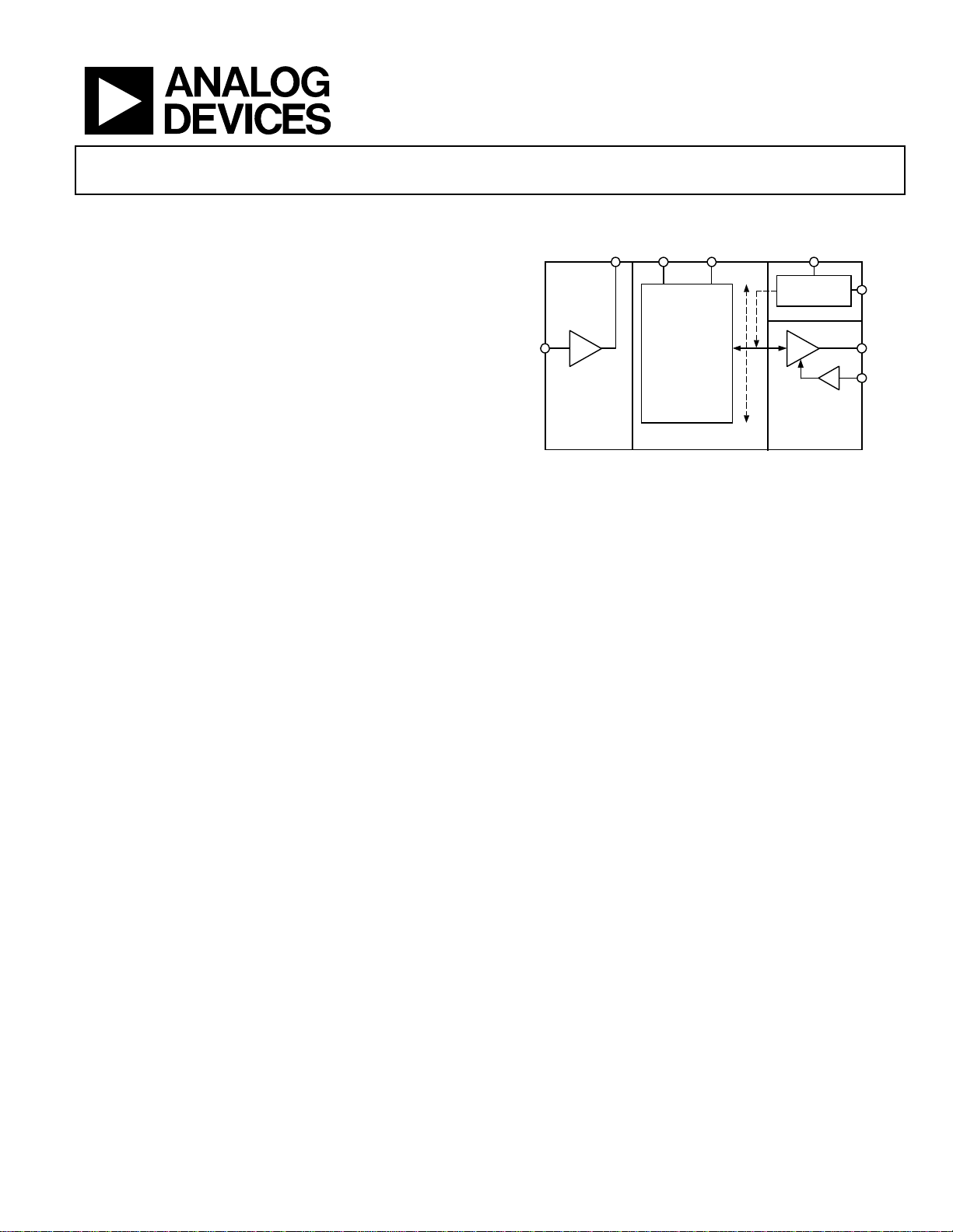
FUNCTIONAL BLOCK DIAGRAM
PAOx
PROGRAMMABLE
ULTRALOW NOISE
PREAMPLIFIER
G = 14dB TO 20dB
DSXx
DIFFERENTIAL
ATTENUATOR
LADDER NETWORK
0dB TO –48.4dB
PRECISION PASSIVE
INPUT AT TENUATOR
R-1.5R
Figure 1.
+DSXx
AD604
GNx
GAIN CONT ROL
AND SCALING
AFA
FIXED GAIN
AMPLIFIER
34.4dB
VREF
OUTx
VOCM
00540-001
Rev. F
Information furnished by Analog Devices is believed to be accurate and reliable. However, no
responsibility is assumed by Analog Devices for its use, nor for any infringements of patents or other
rights of third parties that may result from its use. Specifications subject to change without notice. No
license is granted by implication or otherwise under any patent or patent rights of Analog Devices.
Trademarks and registered trademarks are the property of their respective owners.
WWW.100Y.COM.TW WWW.100Y.COM.TW WWW.100Y.COM.TW
WWW.100Y.COM.TW WWW.100Y.COM.TW WWW.100Y.COM.TW
WWW.100Y.COM.TW WWW.100Y.COM.TW WWW.100Y.COM.TW
One Technology Way, P.O. Box 9106, Norwood, MA 02062-9106, U.S.A.
Tel: 781.329.4700 www.analog.com
Fax: 781.461.3113 ©1996–2010 Analog Devices, Inc. All rights reserved.
WWW.100Y.COM.TW WWW.100Y.COM.TW WWW.100Y.COM.TW
WWW.100Y.COM.TW WWW.100Y.COM.TW WWW.100Y.COM.TW
Page 2

AD604
TABLE OF CONTENTS
Features .............................................................................................. 1
Applications ....................................................................................... 1
Functional Block Diagram .............................................................. 1
General Description ......................................................................... 1
Revision History ............................................................................... 2
Specifications ..................................................................................... 3
WWW.100Y.COM.TW WWW.100Y.COM.TW WWW.100Y.COM.TW
Absolute Maximum Ratings ............................................................ 5
ESD Caution .................................................................................. 5
WWW.100Y.COM.TW WWW.100Y.COM.TW WWW.100Y.COM.TW
Pin Configuration and Function Descriptions ............................. 6
WWW.100Y.COM.TW WWW.100Y.COM.TW WWW.100Y.COM.TW
Typical Performance Characteristics ............................................. 7
WWW.100Y.COM.TW WWW.100Y.COM.TW WWW.100Y.COM.TW
Theory of Operation ...................................................................... 13
Preamplifier ................................................................................. 14
WWW.100Y.COM.TW WWW.100Y.COM.TW WWW.100Y.COM.TW
Differential Ladder (Attenuator) .............................................. 15
WWW.100Y.COM.TW WWW.100Y.COM.TW WWW.100Y.COM.TW
AC Coupling ............................................................................... 16
WWW.100Y.COM.TW WWW.100Y.COM.TW WWW.100Y.COM.TW
Gain Control Interface ............................................................... 16
WWW.100Y.COM.TW WWW.100Y.COM.TW WWW.100Y.COM.TW
Active Feedback Amplifier (Fixed-Gain Amp) ...................... 16
WWW.100Y.COM.TW WWW.100Y.COM.TW WWW.100Y.COM.TW
WWW.100Y.COM.TW WWW.100Y.COM.TW WWW.100Y.COM.TW
REVISION HISTORY
4/10—Rev. E to Rev. F
Changes to Figure 55, DSX Input Connections Section, and
Differential DSX Inputs Section .............................................. 24
Changes to Figure 61, Deleted Table 6 ......................................... 27
Changes to Ordering Guide .......................................................... 29
10/08—Rev. D to Rev. E
Changes to Figure 1 .......................................................................... 1
Changes to Figure 37 ...................................................................... 13
Changes to Figure 41 ...................................................................... 15
Changes to Evaluation Board Model Name ................................ 24
Changes to Ordering Guide .......................................................... 29
1/08—Rev. C to Rev. D
Changes to AC Coupling Section ................................................. 16
Changes to Applications Information Section ............................ 18
Changes to An Ultralow Noise AGC Amplifier with 82 dB to
96 dB Gain Range Section ............................................................. 19
Changes to Figure 55 and Figure 56 ............................................. 24
Changes to Cascaded DSX Section and Outputs Section ......... 25
Changes to Figure 57 to Figure 60 ................................................ 26
Changes to Figure 61 and Table 6 ................................................. 27
Changes to Ordering Guide .......................................................... 29
WWW.100Y.COM.TW WWW.100Y.COM.TW WWW.100Y.COM.TW
WWW.100Y.COM.TW WWW.100Y.COM.TW WWW.100Y.COM.TW
WWW.100Y.COM.TW WWW.100Y.COM.TW WWW.100Y.COM.TW
WWW.100Y.COM.TW WWW.100Y.COM.TW WWW.100Y.COM.TW
WWW.100Y.COM.TW WWW.100Y.COM.TW WWW.100Y.COM.TW
WWW.100Y.COM.TW WWW.100Y.COM.TW WWW.100Y.COM.TW
WWW.100Y.COM.TW WWW.100Y.COM.TW WWW.100Y.COM.TW
WWW.100Y.COM.TW WWW.100Y.COM.TW WWW.100Y.COM.TW
WWW.100Y.COM.TW WWW.100Y.COM.TW WWW.100Y.COM.TW
WWW.100Y.COM.TW WWW.100Y.COM.TW WWW.100Y.COM.TW
WWW.100Y.COM.TW WWW.100Y.COM.TW WWW.100Y.COM.TW
WWW.100Y.COM.TW WWW.100Y.COM.TW WWW.100Y.COM.TW
WWW.100Y.COM.TW WWW.100Y.COM.TW WWW.100Y.COM.TW
WWW.100Y.COM.TW WWW.100Y.COM.TW WWW.100Y.COM.TW
WWW.100Y.COM.TW WWW.100Y.COM.TW WWW.100Y.COM.TW
WWW.100Y.COM.TW WWW.100Y.COM.TW WWW.100Y.COM.TW
WWW.100Y.COM.TW WWW.100Y.COM.TW WWW.100Y.COM.TW
Applications Information .............................................................. 18
Ultralow Noise AGC Amplifier with 82 dB to 96 dB
Gain Range .................................................................................. 19
Ultralow Noise, Differential Input-Differential
Output VGA ................................................................................ 21
Medical Ultrasound TGC Driving the AD9050, a 10-Bit,
40 MSPS ADC............................................................................. 22
Evaluation Board ............................................................................ 24
Using the Preamplifier ............................................................... 24
DSX Input Connections ............................................................ 24
Preamplifier Gain ....................................................................... 25
Outputs ........................................................................................ 25
DC Operating Conditions ......................................................... 25
Evaluation Board Artwork and Schematic ............................. 26
Outline Dimensions ....................................................................... 28
Ordering Guide .......................................................................... 29
3/07—Rev. B to Rev. C
Added Evaluation Board Section ................................................. 24
Added Evaluation Board Artwork and Schematics Section ..... 26
Changes to Ordering Guide .......................................................... 29
12/06—Rev. A to Rev. B
Changes to General Description .....................................................1
Changes to Figure 54 ...................................................................... 23
Changes to Ordering Guide .......................................................... 25
1/04—Rev. 0 to Rev. A
Changes to Specifications .................................................................2
Changes to Absolute Maximum Ratings ........................................3
Changes to Ordering Guide .............................................................3
Changes to Figure 1 Caption............................................................5
Changes to Figure 11 Caption .........................................................6
Changes to Figure 17 .........................................................................6
Changes to Figure 51 ...................................................................... 17
Updated Outline Dimensions ....................................................... 18
10/96—Revision 0: Initial Version
WWW.100Y.COM.TW WWW.100Y.COM.TW WWW.100Y.COM.TW
WWW.100Y.COM.TW WWW.100Y.COM.TW WWW.100Y.COM.TW
WWW.100Y.COM.TW WWW.100Y.COM.TW WWW.100Y.COM.TW
WWW.100Y.COM.TW WWW.100Y.COM.TW WWW.100Y.COM.TW
Rev. F | Page 2 of 32
WWW.100Y.COM.TW WWW.100Y.COM.TW WWW.100Y.COM.TW
WWW.100Y.COM.TW WWW.100Y.COM.TW WWW.100Y.COM.TW
Page 3
AD604
SPECIFICATIONS
Each amplifier channel at TA = 25°C, VS = ±5 V, RS = 50 Ω, RL = 500 Ω, CL = 5 pF, V
range (preamplifier gain = 14 dB), VOCM = 2.5 V, C1 and C2 = 0.1 µF (see Figure 37), unless otherwise noted.
Table 1.
Parameter Conditions Min Typ Max Unit
INPUT CHARACTERISTICS
Preamplifier
Input Resistance 300 kΩ
WWW.100Y.COM.TW WWW.100Y.COM.TW WWW.100Y.COM.TW
WWW.100Y.COM.TW WWW.100Y.COM.TW WWW.100Y.COM.TW
WWW.100Y.COM.TW WWW.100Y.COM.TW WWW.100Y.COM.TW
WWW.100Y.COM.TW WWW.100Y.COM.TW WWW.100Y.COM.TW
WWW.100Y.COM.TW WWW.100Y.COM.TW WWW.100Y.COM.TW
WWW.100Y.COM.TW WWW.100Y.COM.TW WWW.100Y.COM.TW
WWW.100Y.COM.TW WWW.100Y.COM.TW WWW.100Y.COM.TW
Input Capacitance 8.5 pF
Input Bias Current −27 mA
Peak Input Voltage Preamplifier gain = 14 dB ±400 mV
Preamplifier gain = 20 dB ±200 mV
Input Voltage Noise VGN = 2.9 V, RS = 0 Ω
Preamplifier gain = 14 dB 0.8 nV/√Hz
Preamplifier gain = 20 dB 0.73 nV/√Hz
Input Current Noise Independent of gain 3.0 pA/√Hz
Noise Figure RS = 50 Ω, f = 10 MHz, VGN = 2.9 V 2.3 dB
R
DSX
WWW.100Y.COM.TW WWW.100Y.COM.TW WWW.100Y.COM.TW
Input Resistance 175 Ω
Input Capacitance 3.0 pF
WWW.100Y.COM.TW WWW.100Y.COM.TW WWW.100Y.COM.TW
Peak Input Voltage 2.5 ± 2 V
WWW.100Y.COM.TW WWW.100Y.COM.TW WWW.100Y.COM.TW
Input Voltage Noise VGN = 2.9 V 1.8 nV/√Hz
Input Current Noise VGN = 2.9 V 2.7 pA/√Hz
WWW.100Y.COM.TW WWW.100Y.COM.TW WWW.100Y.COM.TW
Noise Figure RS = 50 Ω, f = 10 MHz, VGN = 2.9 V 8.4 dB
WWW.100Y.COM.TW WWW.100Y.COM.TW WWW.100Y.COM.TW
R
Common-Mode Rejection Ratio f = 1 MHz, VGN = 2.65 V −20 dB
WWW.100Y.COM.TW WWW.100Y.COM.TW WWW.100Y.COM.TW
OUTPUT CHARACTERISTICS
WWW.100Y.COM.TW WWW.100Y.COM.TW WWW.100Y.COM.TW
−3 dB Bandwidth Constant with gain 40 MHz
Slew Rate VGN = 1.5 V, output = 1 V step 170 V/μs
WWW.100Y.COM.TW WWW.100Y.COM.TW WWW.100Y.COM.TW
Output Signal Range RL ≥ 500 Ω 2.5 ± 1.5 V
Output Impedance f = 10 MHz 2 Ω
Output Short-Circuit Current ±40 mA
Harmonic Distortion VGN = 1 V, V
Two-Tone Intermodulation Distortion (IMD) VGN = 2.9 V, V
f = 10 MHz −71 dBc
Third-Order Intercept
1 dB Compression Point f = 1 MHz, VGN = 2.9 V, output referred 15 dBm
Channel-to-Channel Crosstalk
WWW.100Y.COM.TW WWW.100Y.COM.TW WWW.100Y.COM.TW
WWW.100Y.COM.TW WWW.100Y.COM.TW WWW.100Y.COM.TW
HD2 f = 1 MHz −54 dBc
HD3 f = 1 MHz −67 dBc
HD2 f = 10 MHz −43 dBc
HD3 f = 10 MHz −48 dBc
WWW.100Y.COM.TW WWW.100Y.COM.TW WWW.100Y.COM.TW
WWW.100Y.COM.TW WWW.100Y.COM.TW WWW.100Y.COM.TW
WWW.100Y.COM.TW WWW.100Y.COM.TW WWW.100Y.COM.TW
WWW.100Y.COM.TW WWW.100Y.COM.TW WWW.100Y.COM.TW
f = 1 MHz −74 dBc
WWW.100Y.COM.TW WWW.100Y.COM.TW WWW.100Y.COM.TW
WWW.100Y.COM.TW WWW.100Y.COM.TW WWW.100Y.COM.TW
WWW.100Y.COM.TW WWW.100Y.COM.TW WWW.100Y.COM.TW
WWW.100Y.COM.TW WWW.100Y.COM.TW WWW.100Y.COM.TW
WWW.100Y.COM.TW WWW.100Y.COM.TW WWW.100Y.COM.TW
Group Delay Variation 1 MHz < f < 10 MHz, full gain range ±2 ns
VOCM Input Resistance 45 kΩ
WWW.100Y.COM.TW WWW.100Y.COM.TW WWW.100Y.COM.TW
WWW.100Y.COM.TW WWW.100Y.COM.TW WWW.100Y.COM.TW
= 200 Ω, f = 10 MHz, VGN = 2.9 V 1.1 dB
S
= 200 Ω, f = 10 MHz, VGN = 2.9 V 12 dB
S
= 1 V p-p
OUT
= 1 V p-p
OUT
f = 10 MHz, VGN = 2.65 V, V
input referred
= 1 V p-p, f = 1 MHz,
V
OUT
Channel 1: VGN = 2.65 V, inputs shorted,
Channel 2: VGN = 1.5 V (mid gain)
= 2.50 V (scaling = 20 dB/V), 0 dB to 48 dB gain
REF
= 1 V p-p,
OUT
−12.5 dBm
−30 dB
WWW.100Y.COM.TW WWW.100Y.COM.TW WWW.100Y.COM.TW
WWW.100Y.COM.TW WWW.100Y.COM.TW WWW.100Y.COM.TW
WWW.100Y.COM.TW WWW.100Y.COM.TW WWW.100Y.COM.TW
Rev. F | Page 3 of 32
WWW.100Y.COM.TW WWW.100Y.COM.TW WWW.100Y.COM.TW
WWW.100Y.COM.TW WWW.100Y.COM.TW WWW.100Y.COM.TW
Page 4

AD604
Parameter Conditions Min Typ Max Unit
ACCURACY
Absolute Gain Error
0 dB to 3 dB 0.25 V < VGN < 0.400 V −1.2 +0.75 +3 dB
3 dB to 43 dB 0.400 V < VGN < 2.400 V −1.0 ±0.3 +1.0 dB
43 dB to 48 dB 2.400 V < VGN < 2.65 V −3.5 −1.25 +1.2 dB
Gain Scaling Error 0.400 V < VGN < 2.400 V ±0.25 dB/V
Output Offset Voltage VREF = 2.500 V, VOCM = 2.500 V −50 ±30 +50 mV
Output Offset Variation VREF = 2.500 V, VOCM = 2.500 V 30 50 mV
GAIN CONTROL INTERFACE
WWW.100Y.COM.TW WWW.100Y.COM.TW WWW.100Y.COM.TW
WWW.100Y.COM.TW WWW.100Y.COM.TW WWW.100Y.COM.TW
WWW.100Y.COM.TW WWW.100Y.COM.TW WWW.100Y.COM.TW
Gain Scaling Factor VREF = 2.5 V, 0.4 V < VGN < 2.4 V 19 20 21 dB/V
VREF = 1.67 V 30 dB/V
Gain Range Preamplifier gain = 14 dB 0 to 48 dB
Preamplifier gain = 20 dB 6 to 54 dB
Input Voltage (VGN) Range 20 dB/V, VREF = 2.5 V 0.1 to 2.9 V
WWW.100Y.COM.TW WWW.100Y.COM.TW WWW.100Y.COM.TW
Input Bias Current −0.4 μA
Input Resistance 2 MΩ
WWW.100Y.COM.TW WWW.100Y.COM.TW WWW.100Y.COM.TW
Response Time 48 dB gain change 0.2 μs
WWW.100Y.COM.TW WWW.100Y.COM.TW WWW.100Y.COM.TW
VREF Input Resistance 10 kΩ
WWW.100Y.COM.TW WWW.100Y.COM.TW WWW.100Y.COM.TW
POWER SUPPLY
Specified Operating Range One complete channel ±5 V
WWW.100Y.COM.TW WWW.100Y.COM.TW WWW.100Y.COM.TW
One DSX only 5 V
WWW.100Y.COM.TW WWW.100Y.COM.TW WWW.100Y.COM.TW
Power Dissipation One complete channel 220 mW
One DSX only 95 mW
WWW.100Y.COM.TW WWW.100Y.COM.TW WWW.100Y.COM.TW
Quiescent Supply Current VPOS, one complete channel 32 36 mA
WWW.100Y.COM.TW WWW.100Y.COM.TW WWW.100Y.COM.TW
VPOS, one DSX only 19 23 mA
VNEG, one preamplifier only −15 −12 mA
WWW.100Y.COM.TW WWW.100Y.COM.TW WWW.100Y.COM.TW
Powered Down VPOS, VGN < 50 mV, one channel 1.9 3.0 mA
VNEG, VGN < 50 mV, one channel −150 μA
Power-Up Response Time 48 dB gain change, V
Power-Down Response Time 0.4 μs
WWW.100Y.COM.TW WWW.100Y.COM.TW WWW.100Y.COM.TW
= 2 V p-p 0.6 μs
WWW.100Y.COM.TW WWW.100Y.COM.TW WWW.100Y.COM.TW
OUT
WWW.100Y.COM.TW WWW.100Y.COM.TW WWW.100Y.COM.TW
WWW.100Y.COM.TW WWW.100Y.COM.TW WWW.100Y.COM.TW
WWW.100Y.COM.TW WWW.100Y.COM.TW WWW.100Y.COM.TW
WWW.100Y.COM.TW WWW.100Y.COM.TW WWW.100Y.COM.TW
WWW.100Y.COM.TW WWW.100Y.COM.TW WWW.100Y.COM.TW
WWW.100Y.COM.TW WWW.100Y.COM.TW WWW.100Y.COM.TW
WWW.100Y.COM.TW WWW.100Y.COM.TW WWW.100Y.COM.TW
WWW.100Y.COM.TW WWW.100Y.COM.TW WWW.100Y.COM.TW
WWW.100Y.COM.TW WWW.100Y.COM.TW WWW.100Y.COM.TW
WWW.100Y.COM.TW WWW.100Y.COM.TW WWW.100Y.COM.TW
WWW.100Y.COM.TW WWW.100Y.COM.TW WWW.100Y.COM.TW
WWW.100Y.COM.TW WWW.100Y.COM.TW WWW.100Y.COM.TW
WWW.100Y.COM.TW WWW.100Y.COM.TW WWW.100Y.COM.TW
WWW.100Y.COM.TW WWW.100Y.COM.TW WWW.100Y.COM.TW
WWW.100Y.COM.TW WWW.100Y.COM.TW WWW.100Y.COM.TW
WWW.100Y.COM.TW WWW.100Y.COM.TW WWW.100Y.COM.TW
WWW.100Y.COM.TW WWW.100Y.COM.TW WWW.100Y.COM.TW
Rev. F | Page 4 of 32
WWW.100Y.COM.TW WWW.100Y.COM.TW WWW.100Y.COM.TW
WWW.100Y.COM.TW WWW.100Y.COM.TW WWW.100Y.COM.TW
Page 5
AD604
ABSOLUTE MAXIMUM RATINGS
Table 2.
Parameter
Supply Voltage ±V
Pin 17 to Pin 20 (with Pin 16, Pin 22 = 0 V) ±6.5 V
Input Voltages
Pin 1, Pin 2, Pin 11, Pin 12
Pin 4, Pin 9 ±2 V
WWW.100Y.COM.TW WWW.100Y.COM.TW WWW.100Y.COM.TW
WWW.100Y.COM.TW WWW.100Y.COM.TW WWW.100Y.COM.TW
WWW.100Y.COM.TW WWW.100Y.COM.TW WWW.100Y.COM.TW
WWW.100Y.COM.TW WWW.100Y.COM.TW WWW.100Y.COM.TW
WWW.100Y.COM.TW WWW.100Y.COM.TW WWW.100Y.COM.TW
Pin 5, Pin 8 VPOS, VNEG
Pin 6, Pin 7, Pin 13, Pin 14, Pin 23, Pin 24 VPOS, 0 V
Internal Power Dissipation
PDIP (N) 2.2 W
SOIC (RW) 1.7 W
SSOP (RS) 1.1 W
Operating Temperature Range −40°C to +85°C
Storage Temperature Range −65°C to +150°C
WWW.100Y.COM.TW WWW.100Y.COM.TW WWW.100Y.COM.TW
Lead Temperature, Soldering 60 sec 300°C
3
WWW.100Y.COM.TW WWW.100Y.COM.TW WWW.100Y.COM.TW
θ
JA
AD604AN 105°C/W
WWW.100Y.COM.TW WWW.100Y.COM.TW WWW.100Y.COM.TW
AD604AR 73°C/W
WWW.100Y.COM.TW WWW.100Y.COM.TW WWW.100Y.COM.TW
AD604ARS 112°C/W
3
θ
JC
WWW.100Y.COM.TW WWW.100Y.COM.TW WWW.100Y.COM.TW
AD604AN 35°C/W
WWW.100Y.COM.TW WWW.100Y.COM.TW WWW.100Y.COM.TW
AD604AR 38°C/W
AD604ARS 34°C/W
1
Pin 1, Pin 2, Pin 11 to Pin 14, Pin 23, and Pin 24 are part of a single-supply
circuit. The part is likely to suffer damage if any of these pins are accidentally
connected to VN.
2
When driven from an external low impedance source.
3
Using MIL-STD-883 test method G43-87 with a 1S (2-layer) test board.
1, 2
S
Rating
VPOS/2 ± 2 V
continuous
WWW.100Y.COM.TW WWW.100Y.COM.TW WWW.100Y.COM.TW
WWW.100Y.COM.TW WWW.100Y.COM.TW WWW.100Y.COM.TW
WWW.100Y.COM.TW WWW.100Y.COM.TW WWW.100Y.COM.TW
WWW.100Y.COM.TW WWW.100Y.COM.TW WWW.100Y.COM.TW
WWW.100Y.COM.TW WWW.100Y.COM.TW WWW.100Y.COM.TW
WWW.100Y.COM.TW WWW.100Y.COM.TW WWW.100Y.COM.TW
Stresses above those listed under Absolute Maximum Ratings
may cause permanent damage to the device. This is a stress
rating only; functional operation of the device at these or any
other conditions above those indicated in the operational
section of this specification is not implied. Exposure to absolute
maximum rating conditions for extended periods may affect
device reliability.
ESD CAUTION
WWW.100Y.COM.TW WWW.100Y.COM.TW WWW.100Y.COM.TW
WWW.100Y.COM.TW WWW.100Y.COM.TW WWW.100Y.COM.TW
WWW.100Y.COM.TW WWW.100Y.COM.TW WWW.100Y.COM.TW
WWW.100Y.COM.TW WWW.100Y.COM.TW WWW.100Y.COM.TW
WWW.100Y.COM.TW WWW.100Y.COM.TW WWW.100Y.COM.TW
WWW.100Y.COM.TW WWW.100Y.COM.TW WWW.100Y.COM.TW
WWW.100Y.COM.TW WWW.100Y.COM.TW WWW.100Y.COM.TW
WWW.100Y.COM.TW WWW.100Y.COM.TW WWW.100Y.COM.TW
WWW.100Y.COM.TW WWW.100Y.COM.TW WWW.100Y.COM.TW
WWW.100Y.COM.TW WWW.100Y.COM.TW WWW.100Y.COM.TW
WWW.100Y.COM.TW WWW.100Y.COM.TW WWW.100Y.COM.TW
WWW.100Y.COM.TW WWW.100Y.COM.TW WWW.100Y.COM.TW
WWW.100Y.COM.TW WWW.100Y.COM.TW WWW.100Y.COM.TW
WWW.100Y.COM.TW WWW.100Y.COM.TW WWW.100Y.COM.TW
Rev. F | Page 5 of 32
WWW.100Y.COM.TW WWW.100Y.COM.TW WWW.100Y.COM.TW
WWW.100Y.COM.TW WWW.100Y.COM.TW WWW.100Y.COM.TW
Page 6
AD604
–
+
+
–
PIN CONFIGURATION AND FUNCTION DESCRIPTIONS
1
DSX1
DSX1 2
PAO1 3
4
FBK1
PAI1 5
COM1 6
COM2
PAI2 8 VPOS17
FBK2 9 GND216
WWW.100Y.COM.TW WWW.100Y.COM.TW WWW.100Y.COM.TW
WWW.100Y.COM.TW WWW.100Y.COM.TW WWW.100Y.COM.TW
PAO2
DSX2 11 VOCM14
DSX2 12 VGN213
WWW.100Y.COM.TW WWW.100Y.COM.TW WWW.100Y.COM.TW
WWW.100Y.COM.TW WWW.100Y.COM.TW WWW.100Y.COM.TW
Table 3. Pin Function Descriptions
WWW.100Y.COM.TW WWW.100Y.COM.TW WWW.100Y.COM.TW
Pin No. Mnemonic Description
WWW.100Y.COM.TW WWW.100Y.COM.TW WWW.100Y.COM.TW
1 –DSX1 Channel 1 Negative Signal Input to DSX1.
WWW.100Y.COM.TW WWW.100Y.COM.TW WWW.100Y.COM.TW
2 +DSX1 Channel 1 Positive Signal Input to DSX1.
3 PAO1 Channel 1 Preamplifier Output.
WWW.100Y.COM.TW WWW.100Y.COM.TW WWW.100Y.COM.TW
4 FBK1 Channel 1 Preamplifier Feedback Pin.
WWW.100Y.COM.TW WWW.100Y.COM.TW WWW.100Y.COM.TW
5 PAI1 Channel 1 Preamplifier Positive Input.
6 COM1 Channel 1 Signal Ground. When this pin is connected to positive supply, Preamplifier 1 shuts down.
WWW.100Y.COM.TW WWW.100Y.COM.TW WWW.100Y.COM.TW
7 COM2 Channel 2 Signal Ground. When this pin is connected to positive supply, Preamplifier 2 shuts down.
8 PAI2 Channel 2 Preamplifier Positive Input.
9 FBK2 Channel 2 Preamplifier Feedback Pin.
10 PAO2 Channel 2 Preamplifier Output.
11 +DSX2 Channel 2 Positive Signal Input to DSX2.
12 –DSX2 Channel 2 Negative Signal Input to DSX2.
13 VGN2
14 VOCM Input to this pin defines the common mode of the output at OUT1 and OUT2.
15 OUT2 Channel 2 Signal Output.
16 GND2 Ground.
17 VPOS Positive Supply.
18 VNEG Negative Supply.
19 VNEG Negative Supply.
20 VPOS Positive Supply.
21 GND1 Ground.
22 OUT1 Channel 1 Signal Output.
23 VREF Input to this pin sets gain scaling for both channels to 2.5 V = 20 dB/V and 1.67 V = 30 dB/V.
24 VGN1
WWW.100Y.COM.TW WWW.100Y.COM.TW WWW.100Y.COM.TW
WWW.100Y.COM.TW WWW.100Y.COM.TW WWW.100Y.COM.TW
WWW.100Y.COM.TW WWW.100Y.COM.TW WWW.100Y.COM.TW
WWW.100Y.COM.TW WWW.100Y.COM.TW WWW.100Y.COM.TW
WWW.100Y.COM.TW WWW.100Y.COM.TW WWW.100Y.COM.TW
Channel 2 Gain Control Input and Power-Down Pin. If this pin is grounded, the device is off; otherwise, positive
voltage increases gain.
WWW.100Y.COM.TW WWW.100Y.COM.TW WWW.100Y.COM.TW
WWW.100Y.COM.TW WWW.100Y.COM.TW WWW.100Y.COM.TW
WWW.100Y.COM.TW WWW.100Y.COM.TW WWW.100Y.COM.TW
WWW.100Y.COM.TW WWW.100Y.COM.TW WWW.100Y.COM.TW
WWW.100Y.COM.TW WWW.100Y.COM.TW WWW.100Y.COM.TW
WWW.100Y.COM.TW WWW.100Y.COM.TW WWW.100Y.COM.TW
WWW.100Y.COM.TW WWW.100Y.COM.TW WWW.100Y.COM.TW
Channel 1 Gain Control Input and Power-Down Pin. If this pin is grounded, the device is off; otherwise, positive
WWW.100Y.COM.TW WWW.100Y.COM.TW WWW.100Y.COM.TW
voltage increases gain.
WWW.100Y.COM.TW WWW.100Y.COM.TW WWW.100Y.COM.TW
AD604
TOP VIEW
7
(Not to Scale)
10
Figure 2. Pin Configuration
24
VGN1
VREF23
OUT122
21
GND1
VPOS20
VNEG19
18
VNEG
15
OUT2
00540-002
WWW.100Y.COM.TW WWW.100Y.COM.TW WWW.100Y.COM.TW
WWW.100Y.COM.TW WWW.100Y.COM.TW WWW.100Y.COM.TW
WWW.100Y.COM.TW WWW.100Y.COM.TW WWW.100Y.COM.TW
WWW.100Y.COM.TW WWW.100Y.COM.TW WWW.100Y.COM.TW
WWW.100Y.COM.TW WWW.100Y.COM.TW WWW.100Y.COM.TW
WWW.100Y.COM.TW WWW.100Y.COM.TW WWW.100Y.COM.TW
WWW.100Y.COM.TW WWW.100Y.COM.TW WWW.100Y.COM.TW
Rev. F | Page 6 of 32
WWW.100Y.COM.TW WWW.100Y.COM.TW WWW.100Y.COM.TW
WWW.100Y.COM.TW WWW.100Y.COM.TW WWW.100Y.COM.TW
Page 7
AD604
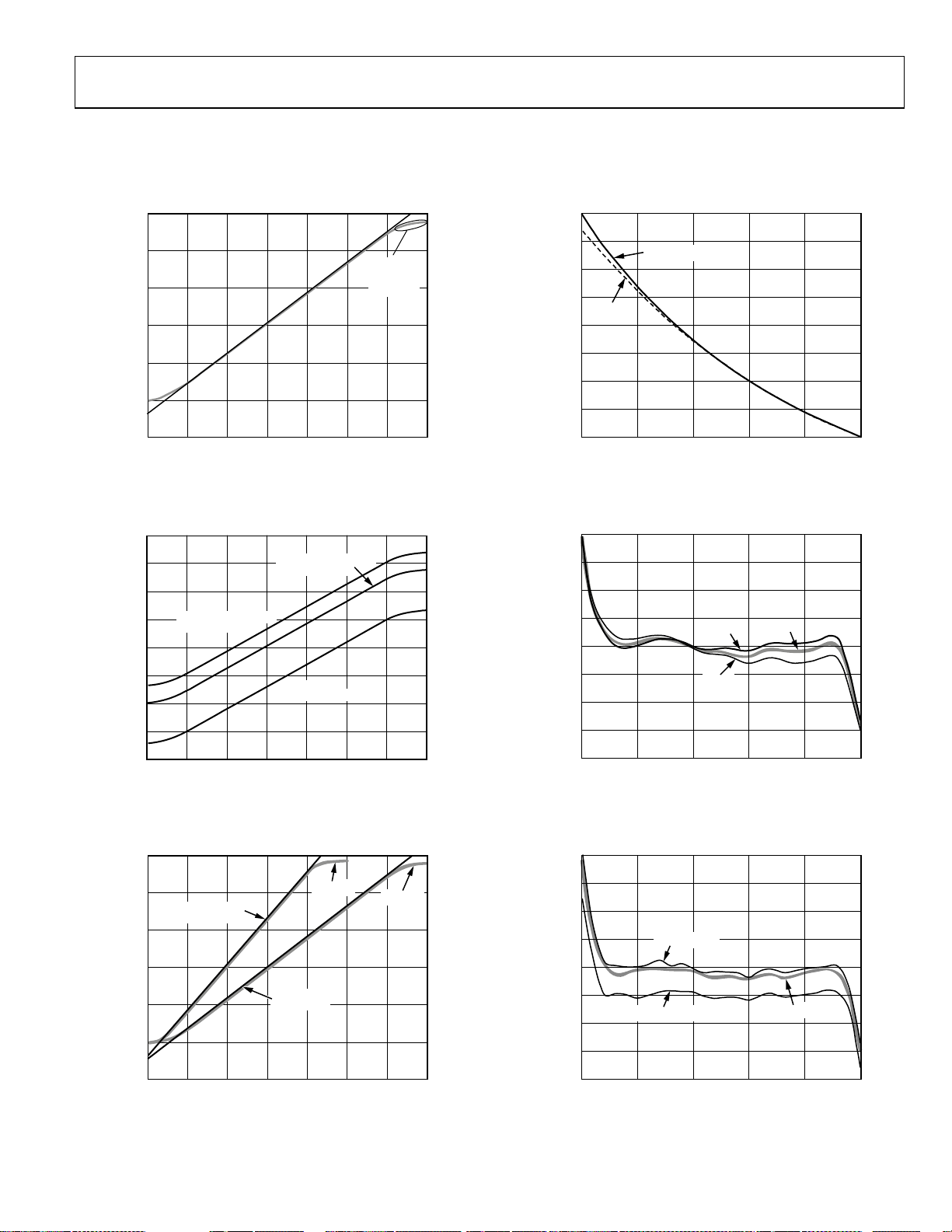
TYPICAL PERFORMANCE CHARACTERISTICS
Unless otherwise noted, G (preamplifier) = 14 dB, VREF = 2.5 V (20 dB/V scaling), f = 1 MHz, RL = 500 Ω, CL = 5 pF, TA = 25°C, and
V
= ±5 V.
SS
50
40.0
40
30
WWW.100Y.COM.TW WWW.100Y.COM.TW WWW.100Y.COM.TW
WWW.100Y.COM.TW WWW.100Y.COM.TW WWW.100Y.COM.TW
20
GAIN (dB)
10
3 CURVES
–40°C,
+25°C,
+85°C
WWW.100Y.COM.TW WWW.100Y.COM.TW WWW.100Y.COM.TW
WWW.100Y.COM.TW WWW.100Y.COM.TW WWW.100Y.COM.TW
0
WWW.100Y.COM.TW WWW.100Y.COM.TW WWW.100Y.COM.TW
WWW.100Y.COM.TW WWW.100Y.COM.TW WWW.100Y.COM.TW
–10
0.1 0.5 0.9 1.3 1.7 2.1 2.5 2.9
VGN (V)
Figure 3. Gain vs. VGN for Three Temperatures
00540-003
37.5
35.0
32.5
ACTUAL
30.0
27.5
GAIN SCALING (dB/V)
25.0
22.5
20.0
1.25 1.50 1.75 2.00 2.25 2.50
THEORETICAL
Figure 6. Gain Scaling vs. VREF
WWW.100Y.COM.TW WWW.100Y.COM.TW WWW.100Y.COM.TW
WWW.100Y.COM.TW WWW.100Y.COM.TW WWW.100Y.COM.TW
WWW.100Y.COM.TW WWW.100Y.COM.TW WWW.100Y.COM.TW
60
50
WWW.100Y.COM.TW WWW.100Y.COM.TW WWW.100Y.COM.TW
40
WWW.100Y.COM.TW WWW.100Y.COM.TW WWW.100Y.COM.TW
WWW.100Y.COM.TW WWW.100Y.COM.TW WWW.100Y.COM.TW
WWW.100Y.COM.TW WWW.100Y.COM.TW WWW.100Y.COM.TW
GAIN (dB)
30
20
10
G (PREAMP) = +20dB
(+6dB TO +54dB)
WWW.100Y.COM.TW WWW.100Y.COM.TW WWW.100Y.COM.TW
0
G (PREAMP) = +14dB
(0dB TO +48dB)
DSX ONLY
(–14dB TO +34dB)
2.0
1.5
1.0
0.5
0
–0.5
GAIN ERROR (d B)
–1.0
WWW.100Y.COM.TW WWW.100Y.COM.TW WWW.100Y.COM.TW
–10
WWW.100Y.COM.TW WWW.100Y.COM.TW WWW.100Y.COM.TW
–20
0.1 0.5 0.9 1.3 1.7 2.1 2.5 2.9
WWW.100Y.COM.TW WWW.100Y.COM.TW WWW.100Y.COM.TW
WWW.100Y.COM.TW WWW.100Y.COM.TW WWW.100Y.COM.TW
Figure 4. Gain vs. VGN for Different Preamplifier Gains
VGN (V)
00540-004
–1.5
–2.0
0.2 0.7 1.2 1.7 2.2 2.7
Figure 7. Gain Error vs. VGN
WWW.100Y.COM.TW WWW.100Y.COM.TW WWW.100Y.COM.TW
VREF (V)
–40°C
+85°C
VGN (V)
00540-006
+25°C
00540-007
50
40
30
20
GAIN (dB)
10
WWW.100Y.COM.TW WWW.100Y.COM.TW WWW.100Y.COM.TW
WWW.100Y.COM.TW WWW.100Y.COM.TW WWW.100Y.COM.TW
30dB/V
WWW.100Y.COM.TW WWW.100Y.COM.TW WWW.100Y.COM.TW
VREF = 1.67V
ACTUAL
ACTUAL
WWW.100Y.COM.TW WWW.100Y.COM.TW WWW.100Y.COM.TW
WWW.100Y.COM.TW WWW.100Y.COM.TW WWW.100Y.COM.TW
WWW.100Y.COM.TW WWW.100Y.COM.TW WWW.100Y.COM.TW
20dB/V
VREF = 2.5V
WWW.100Y.COM.TW WWW.100Y.COM.TW WWW.100Y.COM.TW
0
–10
0.10.50.91.31.72.12.52.9
Figure 5. Gain vs. VGN for Different Gain Scalings
WWW.100Y.COM.TW WWW.100Y.COM.TW WWW.100Y.COM.TW
WWW.100Y.COM.TW WWW.100Y.COM.TW WWW.100Y.COM.TW
WWW.100Y.COM.TW WWW.100Y.COM.TW WWW.100Y.COM.TW
VGN (V)
WWW.100Y.COM.TW WWW.100Y.COM.TW WWW.100Y.COM.TW
WWW.100Y.COM.TW WWW.100Y.COM.TW WWW.100Y.COM.TW
WWW.100Y.COM.TW WWW.100Y.COM.TW WWW.100Y.COM.TW
WWW.100Y.COM.TW WWW.100Y.COM.TW WWW.100Y.COM.TW
00540-005
Rev. F | Page 7 of 32
2.0
1.5
1.0
0.5
0
–0.5
GAIN ERROR (d B)
–1.0
–1.5
–2.0
0.2 0.7 1.2 1.7 2.2 2.7
FREQ = 1MHz
FREQ = 10MHz
FREQ = 5MHz
VGN (V)
Figure 8. Gain Error vs. VGN at Different Frequencies
00540-008
Page 8
AD604
2.0
1.5
1.0
0.5
0
–0.5
GAIN ERROR (d B)
–1.0
WWW.100Y.COM.TW WWW.100Y.COM.TW WWW.100Y.COM.TW
WWW.100Y.COM.TW WWW.100Y.COM.TW WWW.100Y.COM.TW
–1.5
–2.0
0.2 0.7 1.2 1.7 2.2 2.7
WWW.100Y.COM.TW WWW.100Y.COM.TW WWW.100Y.COM.TW
30dB/V
VREF = 1.67V
VGN (V)
20dB/V
VREF = 2.5V
00540-009
Figure 9. Gain Error vs. VGN for Two Gain Scaling Values
50
VGN = 2.5V
40
30
20
10
GAIN (dB)
–10
–20
–30
–40
–50
VGN = 1.5V
VGN = 0.5V
0
VGN = 0.1V
VGN = 0V
100k 1M 10M 100M
FREQUENCY (Hz)
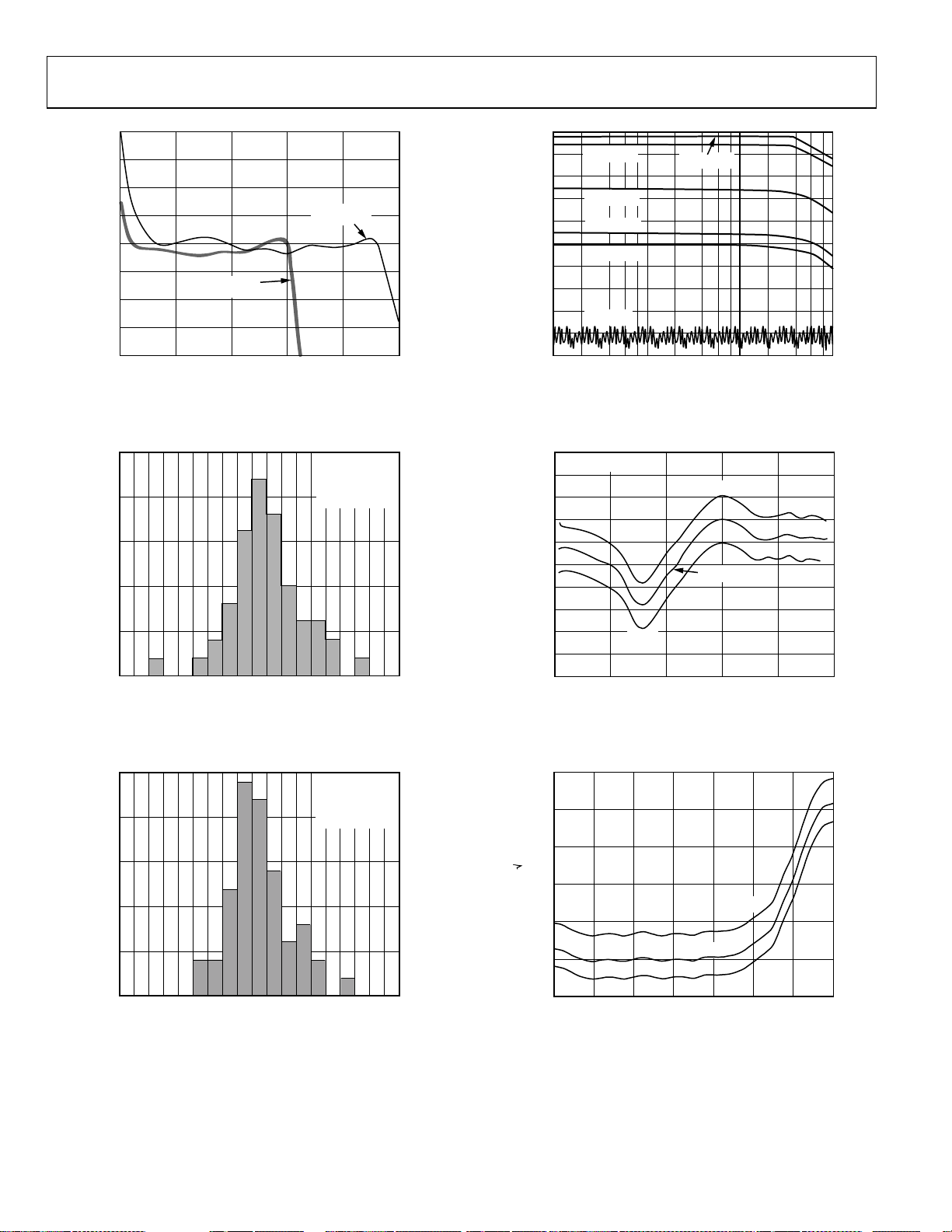
Figure 12. AC Response for Various Values of VGN
WWW.100Y.COM.TW WWW.100Y.COM.TW WWW.100Y.COM.TW
WWW.100Y.COM.TW WWW.100Y.COM.TW WWW.100Y.COM.TW
WWW.100Y.COM.TW WWW.100Y.COM.TW WWW.100Y.COM.TW
25
WWW.100Y.COM.TW WWW.100Y.COM.TW WWW.100Y.COM.TW
20
N=50
VGN1 = 1.0V
VGN2 = 1.0V
ΔG(dB) =
G(CH1)– G(CH2)
WWW.100Y.COM.TW WWW.100Y.COM.TW WWW.100Y.COM.TW
15
WWW.100Y.COM.TW WWW.100Y.COM.TW WWW.100Y.COM.TW
WWW.100Y.COM.TW WWW.100Y.COM.TW WWW.100Y.COM.TW
10
PERCENTAGE
WWW.100Y.COM.TW WWW.100Y.COM.TW WWW.100Y.COM.TW
5
WWW.100Y.COM.TW WWW.100Y.COM.TW WWW.100Y.COM.TW
WWW.100Y.COM.TW WWW.100Y.COM.TW WWW.100Y.COM.TW
0
–1.0 –0.8 –0.6 –0.4 –0.2 0.1 0.3 0.5 0.7 0.9
WWW.100Y.COM.TW WWW.100Y.COM.TW WWW.100Y.COM.TW
WWW.100Y.COM.TW WWW.100Y.COM.TW WWW.100Y.COM.TW
Figure 10. Gain Match; VGN1 = VGN2 = 1.0 V
DELTA GAIN (dB)
00540-010
2.55
VOCM = 2.5V
2.54
2.53
2.52
2.51
(V)
2.50
OUT
V
2.49
2.48
2.47
2.46
2.45
0.2 0.7 1.2 1.7 2.2 2.7
+85°C
Figure 13. Output Offset vs. VGN for Three Temperatures
WWW.100Y.COM.TW WWW.100Y.COM.TW WWW.100Y.COM.TW
VGN = 2.9V
00540-012
–40°C
+25°C
00540-013
VGN (V)
25
20
15
WWW.100Y.COM.TW WWW.100Y.COM.TW WWW.100Y.COM.TW
WWW.100Y.COM.TW WWW.100Y.COM.TW WWW.100Y.COM.TW
WWW.100Y.COM.TW WWW.100Y.COM.TW WWW.100Y.COM.TW
N=50
VGN1 = 2.50V
VGN2 = 2.50V
ΔG(dB) =
G(CH1) – G( CH2)
WWW.100Y.COM.TW WWW.100Y.COM.TW WWW.100Y.COM.TW
WWW.100Y.COM.TW WWW.100Y.COM.TW WWW.100Y.COM.TW
10
PERCENTAGE
WWW.100Y.COM.TW WWW.100Y.COM.TW WWW.100Y.COM.TW
WWW.100Y.COM.TW WWW.100Y.COM.TW WWW.100Y.COM.TW
5
WWW.100Y.COM.TW WWW.100Y.COM.TW WWW.100Y.COM.TW
0
–1.0 –0.8 –0.6 –0.4 –0.2 0.1 0.3 0.5 0.7 0.9
Figure 11. Gain Match; VGN1 = VGN2 = 2.50 V
WWW.100Y.COM.TW WWW.100Y.COM.TW WWW.100Y.COM.TW
WWW.100Y.COM.TW WWW.100Y.COM.TW WWW.100Y.COM.TW
DELTA GAIN (dB)
WWW.100Y.COM.TW WWW.100Y.COM.TW WWW.100Y.COM.TW
WWW.100Y.COM.TW WWW.100Y.COM.TW WWW.100Y.COM.TW
WWW.100Y.COM.TW WWW.100Y.COM.TW WWW.100Y.COM.TW
WWW.100Y.COM.TW WWW.100Y.COM.TW WWW.100Y.COM.TW
WWW.100Y.COM.TW WWW.100Y.COM.TW WWW.100Y.COM.TW
WWW.100Y.COM.TW WWW.100Y.COM.TW WWW.100Y.COM.TW
WWW.100Y.COM.TW WWW.100Y.COM.TW WWW.100Y.COM.TW
00540-011
Rev. F | Page 8 of 32
210
190
170
Hz)
150
NOISE (n V/
130
110
90
0.10.50.91.31.72.12.52.
VGN (V)
+85°C
+25°C
–40°C
Figure 14. Output Referred Noise vs. VGN for Three Temperatures
00540-014
9
Page 9
AD604
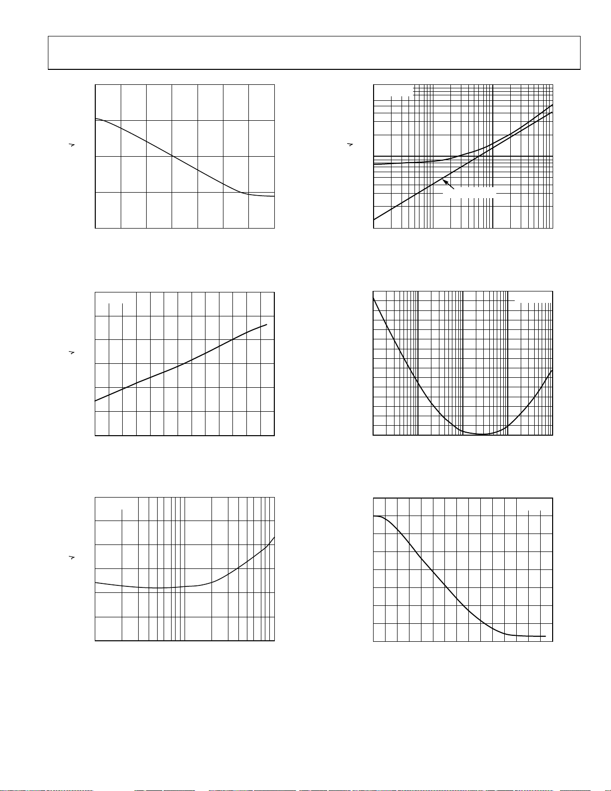
1000
100
10
10
VGN = 2.9V
Hz)
1
NOISE (nV/ Hz)
1
NOISE (n V/
WWW.100Y.COM.TW WWW.100Y.COM.TW WWW.100Y.COM.TW
WWW.100Y.COM.TW WWW.100Y.COM.TW WWW.100Y.COM.TW
WWW.100Y.COM.TW WWW.100Y.COM.TW WWW.100Y.COM.TW
WWW.100Y.COM.TW WWW.100Y.COM.TW WWW.100Y.COM.TW
0.1
0.1 0.5 0.9 1.3 1.7 2.1 2.5 2.9
VGN (V)
Figure 15. Input Referred Noise vs. VGN
00540-015
0.1
110100
Figure 18. Input Referred Noise vs. R
WWW.100Y.COM.TW WWW.100Y.COM.TW WWW.100Y.COM.TW
900
WWW.100Y.COM.TW WWW.100Y.COM.TW WWW.100Y.COM.TW
WWW.100Y.COM.TW WWW.100Y.COM.TW WWW.100Y.COM.TW
WWW.100Y.COM.TW WWW.100Y.COM.TW WWW.100Y.COM.TW
VGN = 2.9V
850
800
WWW.100Y.COM.TW WWW.100Y.COM.TW WWW.100Y.COM.TW
750
WWW.100Y.COM.TW WWW.100Y.COM.TW WWW.100Y.COM.TW
NOISE (pV / Hz)
700
WWW.100Y.COM.TW WWW.100Y.COM.TW WWW.100Y.COM.TW
WWW.100Y.COM.TW WWW.100Y.COM.TW WWW.100Y.COM.TW
650
WWW.100Y.COM.TW WWW.100Y.COM.TW WWW.100Y.COM.TW
600
–40 –20 0 20 40 60 80 90
WWW.100Y.COM.TW WWW.100Y.COM.TW WWW.100Y.COM.TW
WWW.100Y.COM.TW WWW.100Y.COM.TW WWW.100Y.COM.TW
Figure 16. Input Referred Noise vs. Temperature
TEMPERATURE (°C)
00540-016
16
15
14
13
12
11
10
9
8
7
6
NOISE FI GURE (dB)
5
4
3
2
1
101
Figure 19. Noise Figure vs. R
WWW.100Y.COM.TW WWW.100Y.COM.TW WWW.100Y.COM.TW
R
SOURCE
R
SOURCE
R
SOURCE
ALONE
(Ω)
(Ω)
SOURCE
SOURCE
VGN = 2.9V
00540-018
1k
00540-019
10k100 1k
WWW.100Y.COM.TW WWW.100Y.COM.TW WWW.100Y.COM.TW
770
VGN = 2.9V
WWW.100Y.COM.TW WWW.100Y.COM.TW WWW.100Y.COM.TW
765
WWW.100Y.COM.TW WWW.100Y.COM.TW WWW.100Y.COM.TW
760
755
NOISE (pV/ Hz)
750
WWW.100Y.COM.TW WWW.100Y.COM.TW WWW.100Y.COM.TW
WWW.100Y.COM.TW WWW.100Y.COM.TW WWW.100Y.COM.TW
WWW.100Y.COM.TW WWW.100Y.COM.TW WWW.100Y.COM.TW
WWW.100Y.COM.TW WWW.100Y.COM.TW WWW.100Y.COM.TW
745
740
100k 1M 10M
Figure 17. Input Referred Noise vs. Frequency
WWW.100Y.COM.TW WWW.100Y.COM.TW WWW.100Y.COM.TW
WWW.100Y.COM.TW WWW.100Y.COM.TW WWW.100Y.COM.TW
WWW.100Y.COM.TW WWW.100Y.COM.TW WWW.100Y.COM.TW
FREQUENCY (Hz)
WWW.100Y.COM.TW WWW.100Y.COM.TW WWW.100Y.COM.TW
WWW.100Y.COM.TW WWW.100Y.COM.TW WWW.100Y.COM.TW
WWW.100Y.COM.TW WWW.100Y.COM.TW WWW.100Y.COM.TW
WWW.100Y.COM.TW WWW.100Y.COM.TW WWW.100Y.COM.TW
WWW.100Y.COM.TW WWW.100Y.COM.TW WWW.100Y.COM.TW
WWW.100Y.COM.TW WWW.100Y.COM.TW WWW.100Y.COM.TW
WWW.100Y.COM.TW WWW.100Y.COM.TW WWW.100Y.COM.TW
00540-017
Rev. F | Page 9 of 32
40
35
30
25
20
15
NOISE FIGURE (dB)
10
5
0
0 0.40.81.21.62.02.42.8
VGN (V)
Figure 20. Noise Figure vs. VGN
RS= 240Ω
00540-020
Page 10
AD604
–
–
–
–
40
VO=1Vp-p
VGN = 1V
–45
–50
–55
–60
HARMONIC DIST ORTION ( dBc)
WWW.100Y.COM.TW WWW.100Y.COM.TW WWW.100Y.COM.TW
WWW.100Y.COM.TW WWW.100Y.COM.TW WWW.100Y.COM.TW
–65
–70
100k 1M 10M 100M
WWW.100Y.COM.TW WWW.100Y.COM.TW WWW.100Y.COM.TW
WWW.100Y.COM.TW WWW.100Y.COM.TW WWW.100Y.COM.TW
WWW.100Y.COM.TW WWW.100Y.COM.TW WWW.100Y.COM.TW
WWW.100Y.COM.TW WWW.100Y.COM.TW WWW.100Y.COM.TW
WWW.100Y.COM.TW WWW.100Y.COM.TW WWW.100Y.COM.TW
WWW.100Y.COM.TW WWW.100Y.COM.TW WWW.100Y.COM.TW
WWW.100Y.COM.TW WWW.100Y.COM.TW WWW.100Y.COM.TW
HARMONIC DISTORTION (dBc)
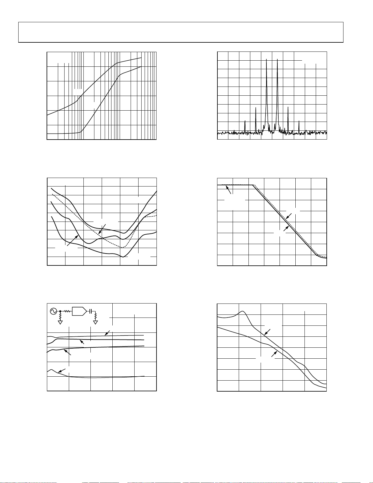
Figure 21. Harmonic Distortion vs. Frequency
30
VO=1Vp-p
–35
–40
–45
–50
–55
WWW.100Y.COM.TW WWW.100Y.COM.TW WWW.100Y.COM.TW
–60
WWW.100Y.COM.TW WWW.100Y.COM.TW WWW.100Y.COM.TW
–65
–70
WWW.100Y.COM.TW WWW.100Y.COM.TW WWW.100Y.COM.TW
–75
WWW.100Y.COM.TW WWW.100Y.COM.TW WWW.100Y.COM.TW
–80
0.5 0.9 1.3 1.7 2.1 2.5 2.9
WWW.100Y.COM.TW WWW.100Y.COM.TW WWW.100Y.COM.TW
HD2
HD3
00540-021
FREQUENCY (Hz)
HD2 (10MHz)
HD3 (10MHz)
HD2 (1MHz)
HD3 (1MHz)
00540-022
WWW.100Y.COM.TW WWW.100Y.COM.TW WWW.100Y.COM.TW
Figure 22. Harmonic Distortion vs. VGN
VGN (V)
20
–30
–40
–50
–60
–70
(dBm)
OUT
–80
P
–90
–100
–110
–120
9.96 9.98 10.00 10.02 10.04
FREQUENCY (MHz)
Figure 24. Intermodulation Distortion
5
0
INPUT
SIGNAL
–5
LIMIT
800mV p-p
–10
–15
(dBm)
IN
P
–20
–25
–30
–35
0.1 0.5 0.9 1.3 1.7 2.1 2.5 2.9
Figure 25. 1 dB Compression vs. VGN
WWW.100Y.COM.TW WWW.100Y.COM.TW WWW.100Y.COM.TW
VGN (V)
1MHz
10MHz
VO=1Vp-p
VGN = 1V
00540-024
00540-025
WWW.100Y.COM.TW WWW.100Y.COM.TW WWW.100Y.COM.TW
R
S
DUT
WWW.100Y.COM.TW WWW.100Y.COM.TW WWW.100Y.COM.TW
50Ω 500Ω
WWW.100Y.COM.TW WWW.100Y.COM.TW WWW.100Y.COM.TW
HD2 (10MHz)
VO=1Vp-p
VGN = 1V
WWW.100Y.COM.TW WWW.100Y.COM.TW WWW.100Y.COM.TW
HD3 (10MHz)
WWW.100Y.COM.TW WWW.100Y.COM.TW WWW.100Y.COM.TW
HD2 (1MHz)
WWW.100Y.COM.TW WWW.100Y.COM.TW WWW.100Y.COM.TW
HD3 (1MHz)
WWW.100Y.COM.TW WWW.100Y.COM.TW WWW.100Y.COM.TW
WWW.100Y.COM.TW WWW.100Y.COM.TW WWW.100Y.COM.TW
0 50 100 150 200 250
Figure 23. Harmonic Distortion vs. R
WWW.100Y.COM.TW WWW.100Y.COM.TW WWW.100Y.COM.TW
R
(Ω)
SOURCE
WWW.100Y.COM.TW WWW.100Y.COM.TW WWW.100Y.COM.TW
SOURCE
WWW.100Y.COM.TW WWW.100Y.COM.TW WWW.100Y.COM.TW
00540-023
25
20
15
10
5
IP3 (dBm)
0
–5
–10
–15
0.4 0.9 1.4 1.9 2.4 2.9
f
f
=10MHz
VGN (V)
=1MHz
Figure 26. Third-Order Intercept vs. VGN
VO=1Vp-p
00540-026
HARMONIC DISTORTION (dBc)
20
–30
–40
–50
–60
–70
–80
WWW.100Y.COM.TW WWW.100Y.COM.TW WWW.100Y.COM.TW
WWW.100Y.COM.TW WWW.100Y.COM.TW WWW.100Y.COM.TW
WWW.100Y.COM.TW WWW.100Y.COM.TW WWW.100Y.COM.TW
WWW.100Y.COM.TW WWW.100Y.COM.TW WWW.100Y.COM.TW
Rev. F | Page 10 of 32
WWW.100Y.COM.TW WWW.100Y.COM.TW WWW.100Y.COM.TW
WWW.100Y.COM.TW WWW.100Y.COM.TW WWW.100Y.COM.TW
Page 11

AD604
V
V
V
2
VO=2Vp-p
VGN = 1.5V
2.9V
100
500mV
90
400mV/DI
VGN (V)
0.1V
10
0%
WWW.100Y.COM.TW WWW.100Y.COM.TW WWW.100Y.COM.TW
WWW.100Y.COM.TW WWW.100Y.COM.TW WWW.100Y.COM.TW
WWW.100Y.COM.TW WWW.100Y.COM.TW WWW.100Y.COM.TW
–2V
253ns 1.253µs
100ns/DIV
Figure 27. Large Signal Pulse Response
00540-027
Figure 30. Gain Response
WWW.100Y.COM.TW WWW.100Y.COM.TW WWW.100Y.COM.TW
WWW.100Y.COM.TW WWW.100Y.COM.TW WWW.100Y.COM.TW
WWW.100Y.COM.TW WWW.100Y.COM.TW WWW.100Y.COM.TW
200
VO=200mVp-p
VGN = 1.5V
WWW.100Y.COM.TW WWW.100Y.COM.TW WWW.100Y.COM.TW
WWW.100Y.COM.TW WWW.100Y.COM.TW WWW.100Y.COM.TW
WWW.100Y.COM.TW WWW.100Y.COM.TW WWW.100Y.COM.TW
40mV/DI
WWW.100Y.COM.TW WWW.100Y.COM.TW WWW.100Y.COM.TW
TRIG'D
WWW.100Y.COM.TW WWW.100Y.COM.TW WWW.100Y.COM.TW
WWW.100Y.COM.TW WWW.100Y.COM.TW WWW.100Y.COM.TW
–200
WWW.100Y.COM.TW WWW.100Y.COM.TW WWW.100Y.COM.TW
253ns 1.253µs
100ns/DIV
00540-028
0
VGN1 = 1V
=1Vp-p
V
OUT1
= GND
V
–10
IN2
–20
VGN2 = 2.9V
–30
VGN2 = 2V
–40
CROSSTALK (dB)
–50
–60
–70
100k 1M 10M 100M
WWW.100Y.COM.TW WWW.100Y.COM.TW WWW.100Y.COM.TW
Figure 28. Small Signal Pulse Response
WWW.100Y.COM.TW WWW.100Y.COM.TW WWW.100Y.COM.TW
Figure 31. Crosstalk (Channel 1 to Channel 2) vs. Frequency
VGN2 = 1.5V
FREQUENCY (Hz)
100ns500mV
VGN2 = 0.1V
0540-030
00540-031
WWW.100Y.COM.TW WWW.100Y.COM.TW WWW.100Y.COM.TW
WWW.100Y.COM.TW WWW.100Y.COM.TW WWW.100Y.COM.TW
500mV
2.9V
WWW.100Y.COM.TW WWW.100Y.COM.TW WWW.100Y.COM.TW
100
90
WWW.100Y.COM.TW WWW.100Y.COM.TW WWW.100Y.COM.TW
WWW.100Y.COM.TW WWW.100Y.COM.TW WWW.100Y.COM.TW
VGN (V)
10
0%
0V
WWW.100Y.COM.TW WWW.100Y.COM.TW WWW.100Y.COM.TW
WWW.100Y.COM.TW WWW.100Y.COM.TW WWW.100Y.COM.TW
WWW.100Y.COM.TW WWW.100Y.COM.TW WWW.100Y.COM.TW
WWW.100Y.COM.TW WWW.100Y.COM.TW WWW.100Y.COM.TW
200ns500mV
00540-029
WWW.100Y.COM.TW WWW.100Y.COM.TW WWW.100Y.COM.TW
Figure 29. Power-Up/Power-Down Response
WWW.100Y.COM.TW WWW.100Y.COM.TW WWW.100Y.COM.TW
0
–10
–20
–30
CMRR (dB)
–40
–50
–60
100k 1M 10M 100M
VGN = 2.9V
VGN = 2.5V
VGN = 2V
VGN = 0.1V
FREQUENCY (Hz)
Figure 32. DSX Common-Mode Rejection Ratio vs. Frequency
00540-032
WWW.100Y.COM.TW WWW.100Y.COM.TW WWW.100Y.COM.TW
WWW.100Y.COM.TW WWW.100Y.COM.TW WWW.100Y.COM.TW
WWW.100Y.COM.TW WWW.100Y.COM.TW WWW.100Y.COM.TW
WWW.100Y.COM.TW WWW.100Y.COM.TW WWW.100Y.COM.TW
WWW.100Y.COM.TW WWW.100Y.COM.TW WWW.100Y.COM.TW
WWW.100Y.COM.TW WWW.100Y.COM.TW WWW.100Y.COM.TW
WWW.100Y.COM.TW WWW.100Y.COM.TW WWW.100Y.COM.TW
Rev. F | Page 11 of 32
Page 12

AD604
WWW.100Y.COM.TW WWW.100Y.COM.TW WWW.100Y.COM.TW
WWW.100Y.COM.TW WWW.100Y.COM.TW WWW.100Y.COM.TW
WWW.100Y.COM.TW WWW.100Y.COM.TW WWW.100Y.COM.TW
WWW.100Y.COM.TW WWW.100Y.COM.TW WWW.100Y.COM.TW
1M
100k
10k
1k
100
INPUT IMPE DANCE (Ω)
10
1
1k 10k 100k 1M 10M 100M
FREQUENCY (Hz)
Figure 33. Input Impedance vs. Frequency
40
+IS(AD604) = +IS(PA) + +IS(DSX)
–I
(AD604)= –IS(PA)
S
35
30
25
20
15
SUPPLY CURRENT ( mA)
10
5
00540-033
0
–40 –20 0 20 40 60 80 90
Figure 35. Supply Current (One Channel) vs. Temperature
DSX (+IS)
+IS(VGN = 0)
TEMPERATURE (°C)
WWW.100Y.COM.TW WWW.100Y.COM.TW WWW.100Y.COM.TW
27.6
WWW.100Y.COM.TW WWW.100Y.COM.TW WWW.100Y.COM.TW
27.4
WWW.100Y.COM.TW WWW.100Y.COM.TW WWW.100Y.COM.TW
27.2
WWW.100Y.COM.TW WWW.100Y.COM.TW WWW.100Y.COM.TW
27.0
WWW.100Y.COM.TW WWW.100Y.COM.TW WWW.100Y.COM.TW
26.8
26.6
WWW.100Y.COM.TW WWW.100Y.COM.TW WWW.100Y.COM.TW
26.4
WWW.100Y.COM.TW WWW.100Y.COM.TW WWW.100Y.COM.TW
INPUT BIAS CURRENT (µA)
26.2
WWW.100Y.COM.TW WWW.100Y.COM.TW WWW.100Y.COM.TW
26.0
WWW.100Y.COM.TW WWW.100Y.COM.TW WWW.100Y.COM.TW
25.8
–40–200 204060809
WWW.100Y.COM.TW WWW.100Y.COM.TW WWW.100Y.COM.TW
WWW.100Y.COM.TW WWW.100Y.COM.TW WWW.100Y.COM.TW
Figure 34. Input Bias Current vs. Temperature
WWW.100Y.COM.TW WWW.100Y.COM.TW WWW.100Y.COM.TW
TEMPERATURE (°C)
00540-034
0
20
18
16
14
12
DELAY ( ns)
10
8
6
100k 1M 10M 100M
VGN = 2.9V
FREQUENCY (Hz)
Figure 36. Group Delay vs. Frequency
WWW.100Y.COM.TW WWW.100Y.COM.TW WWW.100Y.COM.TW
AD604 (+IS)
PREAMP (±IS)
00540-035
VGN = 0.1V
00540-036
WWW.100Y.COM.TW WWW.100Y.COM.TW WWW.100Y.COM.TW
WWW.100Y.COM.TW WWW.100Y.COM.TW WWW.100Y.COM.TW
WWW.100Y.COM.TW WWW.100Y.COM.TW WWW.100Y.COM.TW
WWW.100Y.COM.TW WWW.100Y.COM.TW WWW.100Y.COM.TW
WWW.100Y.COM.TW WWW.100Y.COM.TW WWW.100Y.COM.TW
WWW.100Y.COM.TW WWW.100Y.COM.TW WWW.100Y.COM.TW
WWW.100Y.COM.TW WWW.100Y.COM.TW WWW.100Y.COM.TW
WWW.100Y.COM.TW WWW.100Y.COM.TW WWW.100Y.COM.TW
WWW.100Y.COM.TW WWW.100Y.COM.TW WWW.100Y.COM.TW
WWW.100Y.COM.TW WWW.100Y.COM.TW WWW.100Y.COM.TW
WWW.100Y.COM.TW WWW.100Y.COM.TW WWW.100Y.COM.TW
WWW.100Y.COM.TW WWW.100Y.COM.TW WWW.100Y.COM.TW
WWW.100Y.COM.TW WWW.100Y.COM.TW WWW.100Y.COM.TW
WWW.100Y.COM.TW WWW.100Y.COM.TW WWW.100Y.COM.TW
Rev. F | Page 12 of 32
WWW.100Y.COM.TW WWW.100Y.COM.TW WWW.100Y.COM.TW
WWW.100Y.COM.TW WWW.100Y.COM.TW WWW.100Y.COM.TW
Page 13

AD604
V
x
THEORY OF OPERATION
The AD604 is a dual-channel VGA with an ultralow noise
preamplifier. Figure 37 shows the simplified block diagram of
one channel. Each identical channel consists of a preamplifier
with gain setting resistors (R5, R6, and R7) and a single-supply
X-AMP® (hereafter called DSX, differential single-supply X-AMP)
made up of the following:
• A precision passive attenuator (differential ladder).
• A gain control block.
WWW.100Y.COM.TW WWW.100Y.COM.TW WWW.100Y.COM.TW
WWW.100Y.COM.TW WWW.100Y.COM.TW WWW.100Y.COM.TW
WWW.100Y.COM.TW WWW.100Y.COM.TW WWW.100Y.COM.TW
WWW.100Y.COM.TW WWW.100Y.COM.TW WWW.100Y.COM.TW
• A VOCM buffer with supply splitting resistors
(R3 and R4).
• An active feedback amplifier (AFA) with gain setting
resistors (R1 and R2). To understand the active-feedback
amplifier topology, refer to the AD830 data sheet. The
WWW.100Y.COM.TW WWW.100Y.COM.TW WWW.100Y.COM.TW
WWW.100Y.COM.TW WWW.100Y.COM.TW WWW.100Y.COM.TW
WWW.100Y.COM.TW WWW.100Y.COM.TW WWW.100Y.COM.TW
AD830 is a practical implementation of the idea.
The preamplifier is powered by a ±5 V supply, while the DSX
uses a single +5 V supply. The linear-in-dB gain response of the
AD604 can generally be described by
WWW.100Y.COM.TW WWW.100Y.COM.TW WWW.100Y.COM.TW
G (dB) = Gain Scaling (dB/V) × Gain Control (V) +
(Preamp Gain (dB) − 19 dB) (1)
WWW.100Y.COM.TW WWW.100Y.COM.TW WWW.100Y.COM.TW
Each channel provides between 0 dB to 48.4 dB and 6 dB to 54.4
WWW.100Y.COM.TW WWW.100Y.COM.TW WWW.100Y.COM.TW
dB of gain, depending on the user-determined preamplifier
WWW.100Y.COM.TW WWW.100Y.COM.TW WWW.100Y.COM.TW
gain. The center 40 dB of gain is exactly linear-in-dB while the
gain error increases at the top and bottom of the range. The gain
WWW.100Y.COM.TW WWW.100Y.COM.TW WWW.100Y.COM.TW
of the preamplifier is typically either 14 dB or 20 dB but can be
WWW.100Y.COM.TW WWW.100Y.COM.TW WWW.100Y.COM.TW
set to intermediate values by a single external resistor (see the
Preamplifier section for details). The gain of the DSX can vary
WWW.100Y.COM.TW WWW.100Y.COM.TW WWW.100Y.COM.TW
from −14 dB to +34.4 dB, as determined by the gain control
voltage (VGN). The VREF input establishes the gain scaling;
the useful gain scaling range is between 20 dB/V and 40 dB/V
for a VREF voltage of 2.5 V and 1.25 V, respectively. For
WWW.100Y.COM.TW WWW.100Y.COM.TW WWW.100Y.COM.TW
WWW.100Y.COM.TW WWW.100Y.COM.TW WWW.100Y.COM.TW
WWW.100Y.COM.TW WWW.100Y.COM.TW WWW.100Y.COM.TW
WWW.100Y.COM.TW WWW.100Y.COM.TW WWW.100Y.COM.TW
VREF
VGNx
WWW.100Y.COM.TW WWW.100Y.COM.TW WWW.100Y.COM.TW
EXT.
C1
+DSXxPAOx
C2
–DSXx
PAIx
WWW.100Y.COM.TW WWW.100Y.COM.TW WWW.100Y.COM.TW
WWW.100Y.COM.TW WWW.100Y.COM.TW WWW.100Y.COM.TW
WWW.100Y.COM.TW WWW.100Y.COM.TW WWW.100Y.COM.TW
WWW.100Y.COM.TW WWW.100Y.COM.TW WWW.100Y.COM.TW
OCM
VPOS
WWW.100Y.COM.TW WWW.100Y.COM.TW WWW.100Y.COM.TW
C3
WWW.100Y.COM.TW WWW.100Y.COM.TW WWW.100Y.COM.TW
EXT.
WWW.100Y.COM.TW WWW.100Y.COM.TW WWW.100Y.COM.TW
WWW.100Y.COM.TW WWW.100Y.COM.TW WWW.100Y.COM.TW
R7
40Ω
FBKx
R5
32Ω
R6
8Ω
R3
COMx
200kΩ
R4
200kΩ
Figure 37. Simplified Block Diagram of a Single Channel of the AD604
WWW.100Y.COM.TW WWW.100Y.COM.TW WWW.100Y.COM.TW
example, if the preamp gain is set to 14 dB and VREF is set to
2.50 V (to establish a gain scaling of 20 dB/V), the gain equation
simplifies to
G (dB) = 20 (dB/V) × VGN (V) – 5 dB
The desired gain can then be achieved by setting the unipolar
gain control (VGN) to a voltage within its nominal operating
range of 0.25 V to 2.65 V (for 20 dB/V gain scaling). The gain is
monotonic for a complete gain control voltage range of 0.1 V to
2.9 V. Maximum gain can be achieved at a VGN of 2.9 V.
The inputs VREF and VOCM are common to both channels.
They are decoupled to ground, minimizing interchannel
crosstalk. For the highest gain scaling accuracy, VREF should
have an external low impedance voltage source. For low accuracy
20 dB/V applications, the VREF input can be decoupled with a
capacitor to ground. In this mode, the gain scaling is determined
by the midpoint between VPOS and GND; therefore, care
should be taken to control the supply voltage to 5 V. The input
resistance looking into the VREF pin is 10 kΩ ± 20%.
The DSX portion of the AD604 is a single-supply circuit, and
the VOCM pin is used to establish the dc level of the midpoint
of this portion of the circuit. The VOCM pin only needs an
external decoupling capacitor to ground to center the midpoint
between the supply voltages (5 V, GND); however, the VOCM
can be adjusted to other voltage levels if the dc common-mode
level of the output is important to the user (for example, see the
section entitled Medical Ultrasound TGC Driving the AD9050,
a 10-Bit, 40 MSPS ADC). The input resistance looking into the
VOCM pin is 45 kΩ ± 20%.
GAIN
CONTROL
175Ω
DISTRIBUTED G
G1
G2
175Ω
DIFFERENTIAL
ATTENUATOR
R2
20Ω
R1
820Ω
M
Ao
OUT
00540-037
WWW.100Y.COM.TW WWW.100Y.COM.TW WWW.100Y.COM.TW
WWW.100Y.COM.TW WWW.100Y.COM.TW WWW.100Y.COM.TW
WWW.100Y.COM.TW WWW.100Y.COM.TW WWW.100Y.COM.TW
Rev. F | Page 13 of 32
WWW.100Y.COM.TW WWW.100Y.COM.TW WWW.100Y.COM.TW
WWW.100Y.COM.TW WWW.100Y.COM.TW WWW.100Y.COM.TW
Page 14

AD604
PREAMPLIFIER
The input capability of the following single-supply DSX (2.5 ± 2 V
for a +5 V supply) limits the maximum input voltage of the
preamplifier to ±400 mV for the 14 dB gain configuration or
±200 mV for the 20 dB gain configuration.
The preamplifier gain can be programmed to 14 dB or 20 dB by
either shorting the FBK1 node to PAO1 (14 dB) or by leaving
the FBK1 node open (20 dB). These two gain settings are very
accurate because they are set by the ratio of the on-chip resistors.
Any intermediate gain can be achieved by connecting the
WWW.100Y.COM.TW WWW.100Y.COM.TW WWW.100Y.COM.TW
appropriate resistor value between PAO1 and FBK1 according
to Equation 2 and Equation 3.
WWW.100Y.COM.TW WWW.100Y.COM.TW WWW.100Y.COM.TW
WWW.100Y.COM.TW WWW.100Y.COM.TW WWW.100Y.COM.TW
V
G
WWW.100Y.COM.TW WWW.100Y.COM.TW WWW.100Y.COM.TW
WWW.100Y.COM.TW WWW.100Y.COM.TW WWW.100Y.COM.TW
R
EXT
()
OUT
== (2)
V
IN
[]
= (3)
EXT
6
R
()
()
()
65||7
RRRR
++
7656
RRRGR
×+−×
6567
RRGRR
++×−
WWW.100Y.COM.TW WWW.100Y.COM.TW WWW.100Y.COM.TW
Because the internal resistors have an absolute tolerance of ±20%,
WWW.100Y.COM.TW WWW.100Y.COM.TW WWW.100Y.COM.TW
the gain can be in error by as much as 0.33 dB when R
where it is assumed that R
WWW.100Y.COM.TW WWW.100Y.COM.TW WWW.100Y.COM.TW
Figure 38 shows how the preamplifier is set to gains of 14 dB,
WWW.100Y.COM.TW WWW.100Y.COM.TW WWW.100Y.COM.TW
is exact.
EXT
is 30 Ω,
EXT
17.5 dB, and 20 dB. The gain range of a single channel of the
WWW.100Y.COM.TW WWW.100Y.COM.TW WWW.100Y.COM.TW
AD604 is 0 dB to 48 dB when the preamplifier is set to 14 dB
(Figure 38a), 3.5 dB to 51.5 dB for a preamp gain of 17.5 dB
WWW.100Y.COM.TW WWW.100Y.COM.TW WWW.100Y.COM.TW
(Figure 38b), and 6 dB to 54 dB for the highest preamp gain of
20 dB (Figure 38c).
WWW.100Y.COM.TW WWW.100Y.COM.TW WWW.100Y.COM.TW
WWW.100Y.COM.TW WWW.100Y.COM.TW WWW.100Y.COM.TW
PAI1
WWW.100Y.COM.TW WWW.100Y.COM.TW WWW.100Y.COM.TW
COM1
R6
8Ω
WWW.100Y.COM.TW WWW.100Y.COM.TW WWW.100Y.COM.TW
WWW.100Y.COM.TW WWW.100Y.COM.TW WWW.100Y.COM.TW
a. PREAM P GAIN = 14dB
R5
32Ω
R7
40Ω
PAO1
FBK1
WWW.100Y.COM.TW WWW.100Y.COM.TW WWW.100Y.COM.TW
PAI1
PAO1
WWW.100Y.COM.TW WWW.100Y.COM.TW WWW.100Y.COM.TW
PAO1
FBK1
R10
40Ω
00540-038
Rev. F | Page 14 of 32
R7
R6
WWW.100Y.COM.TW WWW.100Y.COM.TW WWW.100Y.COM.TW
COM1
8Ω
b. PREAMP GAIN= 17.5dB
PAI1
R6
COM1
Figure 38. Preamplifier Gain Programmability
8Ω
For a preamplifier gain of 14 dB, the −3 dB small signal bandwidth
of the preamplifier is 130 MHz. When the gain is at its maximum
of 20 dB, the bandwidth is reduced by half to 65 MHz. Figure 39
shows the ac response for the three preamp gains shown in
Figure 38. Note that the gain for an R
17.5 dB, but the mismatch between the internal resistors and
the external resistor causes the actual gain for this particular
R5
32Ω
WWW.100Y.COM.TW WWW.100Y.COM.TW WWW.100Y.COM.TW
40Ω
FBK1
WWW.100Y.COM.TW WWW.100Y.COM.TW WWW.100Y.COM.TW
WWW.100Y.COM.TW WWW.100Y.COM.TW WWW.100Y.COM.TW
WWW.100Y.COM.TW WWW.100Y.COM.TW WWW.100Y.COM.TW
32Ω
WWW.100Y.COM.TW WWW.100Y.COM.TW WWW.100Y.COM.TW
c. PREAM P GAIN = 20dB
WWW.100Y.COM.TW WWW.100Y.COM.TW WWW.100Y.COM.TW
R7
R5
40Ω
WWW.100Y.COM.TW WWW.100Y.COM.TW WWW.100Y.COM.TW
WWW.100Y.COM.TW WWW.100Y.COM.TW WWW.100Y.COM.TW
WWW.100Y.COM.TW WWW.100Y.COM.TW WWW.100Y.COM.TW
WWW.100Y.COM.TW WWW.100Y.COM.TW WWW.100Y.COM.TW
of 40 Ω should be
EXT
WWW.100Y.COM.TW WWW.100Y.COM.TW WWW.100Y.COM.TW
WWW.100Y.COM.TW WWW.100Y.COM.TW WWW.100Y.COM.TW
WWW.100Y.COM.TW WWW.100Y.COM.TW WWW.100Y.COM.TW
preamplifier to be 17.7 dB. The −3 dB small signal bandwidth of
one complete channel of the AD604 (preamplifier and DSX) is
40 MHz and is independent of gain.
To achieve optimum specifications, power and ground management are critical to the AD604. Large dynamic currents result
because of the low resistances needed for the desired noise
performance. Most of the difficulty is with the very low gain
setting resistors of the preamplifier that allow for a total input
referred noise, including the DSX, as low as 0.8 nV/√Hz. The
consequently large dynamic currents have to be carefully
handled to maintain performance even at large signal levels.
20
19
18
17
16
15
GAIN (dB)
14
13
V
IN
12
11
10
Figure 39. AC Response for Preamplifier Gains of 14 dB, 17.5 dB, and 20 dB
IN
50Ω
8Ω 32Ω
FREQUENCY (Hz)
The preamplifier uses a dual ±5 V supply to accommodate large
dynamic currents and a ground referenced input. The preamplifier
output is also ground referenced and requires a common-mode
level shift into the single-supply DSX. The two external coupling
capacitors (C1 and C2 in Figure 37) connected to the PAO1 and
+DSXx, and –DSXx, nodes and ground, respectively, perform
this function (see the AC Coupling section). In addition, they
eliminate any offset that would otherwise be introduced by the
preamplifier. It should be noted that an offset of 1 mV at the
input of the DSX is amplified by 34.4 dB (× 52.5) when the gain
control voltage is at its maximum; this equates to 52.5 mV at the
output. AC coupling is consequently required to keep the offset
from degrading the output signal range.
The gain-setting preamplifier feedback resistors are small
enough (8 and 32 Ω) that even an additional 1 Ω in the
ground connection at Pin COM1 (the input common-mode
reference) seriously degrades gain accuracy and noise performance.
This node is sensitive, and careful attention is necessary to
minimize the ground impedance. All connections to the COM1
node should be as short as possible.
The preamplifier, including the gain setting resistors, has a
noise performance of 0.71 nV/√Hz and 3 pA/√Hz. Note that a
significant portion of the total input referred voltage noise is
due to the feedback resistors. The equivalent noise resistance
presented by R5 and R6 in parallel is nominally 6.4 Ω, which
contributes 0.33 nV/√Hz to the total input referred voltage noise.
40Ω
40Ω
SHORT
150Ω
R
EXT
OPEN
00540-039
100M10M1M100k
WWW.100Y.COM.TW WWW.100Y.COM.TW WWW.100Y.COM.TW
Page 15

AD604
The larger portion of the input referred voltage noise comes
from the amplifier with 0.63 nV/√Hz. The current noise is
independent of gain and depends only on the bias current in
the input stage of the preamplifier, which is 3 pA/√Hz.
The preamplifier can drive 40 Ω (the nominal feedback resistors)
and the following 175 Ω ladder load of the DSX with low
distortion. For example, at 10 MHz and 1 V at the output, the
preamplifier has less than −45 dB of second and third harmonic
distortion when driven from a low (25 Ω) source resistance.
In applications that require more than 48 dB of gain range, two
WWW.100Y.COM.TW WWW.100Y.COM.TW WWW.100Y.COM.TW
WWW.100Y.COM.TW WWW.100Y.COM.TW WWW.100Y.COM.TW
AD604 channels can be cascaded. Because the preamplifier has
a limited input signal range and consumes over half (120 mW)
of the total power (220 mW), and its ultralow noise is not necessary
WWW.100Y.COM.TW WWW.100Y.COM.TW WWW.100Y.COM.TW
WWW.100Y.COM.TW WWW.100Y.COM.TW WWW.100Y.COM.TW
after the first AD604 channel, a shutdown mechanism that
disables only the preamplifier is provided. To shut down the
preamplifier, connect the COM1 pin and/or COM2 pin to the
WWW.100Y.COM.TW WWW.100Y.COM.TW WWW.100Y.COM.TW
positive supply; the DSX is unaffected. For additional details,
refer to the
WWW.100Y.COM.TW WWW.100Y.COM.TW WWW.100Y.COM.TW
WWW.100Y.COM.TW WWW.100Y.COM.TW WWW.100Y.COM.TW
WWW.100Y.COM.TW WWW.100Y.COM.TW WWW.100Y.COM.TW
WWW.100Y.COM.TW WWW.100Y.COM.TW WWW.100Y.COM.TW
WWW.100Y.COM.TW WWW.100Y.COM.TW WWW.100Y.COM.TW
WWW.100Y.COM.TW WWW.100Y.COM.TW WWW.100Y.COM.TW
DIFFERENTIAL LADDER (ATTENUATOR)
The attenuator before the fixed-gain amplifier of the DSX is
realized by a differential 7-stage R-1.5R resistive ladder network
with an untrimmed input resistance of 175 Ω single-ended or
350 Ω differential. The signal applied at the input of the ladder
Applications Information section.
1
–DSX1
2
+DSX1
3
PAO1
4
FBK1
5
PAI1
6
COM1
AD604
7
COM2
8
PAI2
WWW.100Y.COM.TW WWW.100Y.COM.TW WWW.100Y.COM.TW
WWW.100Y.COM.TW WWW.100Y.COM.TW WWW.100Y.COM.TW
WWW.100Y.COM.TW WWW.100Y.COM.TW WWW.100Y.COM.TW
WWW.100Y.COM.TW WWW.100Y.COM.TW WWW.100Y.COM.TW
9
FBK2
10
PAO2
11
+DSX2
12
–DSX2
Figure 40. Shutdown of Preamplifiers Only
VGN1
VREF
OUT1
GND1
VPOS
VNEG
VNEG
VPOS
GND2
OUT2
VOCM
VGN2
24
23
22
21
20
19
18
17
16
15
14
13
00540-040
WWW.100Y.COM.TW WWW.100Y.COM.TW WWW.100Y.COM.TW
WWW.100Y.COM.TW WWW.100Y.COM.TW WWW.100Y.COM.TW
WWW.100Y.COM.TW WWW.100Y.COM.TW WWW.100Y.COM.TW
WWW.100Y.COM.TW WWW.100Y.COM.TW WWW.100Y.COM.TW
network is attenuated by 6.908 dB per tap; thus, the attenuation
at the first tap is 0 dB, at the second, 13.816 dB, and so on, all
the way to the last tap where the attenuation is 48.356 dB
WWW.100Y.COM.TW WWW.100Y.COM.TW WWW.100Y.COM.TW
WWW.100Y.COM.TW WWW.100Y.COM.TW WWW.100Y.COM.TW
(see Figure 41).
WWW.100Y.COM.TW WWW.100Y.COM.TW WWW.100Y.COM.TW
WWW.100Y.COM.TW WWW.100Y.COM.TW WWW.100Y.COM.TW
–6.908dB
+DSXx
R
WWW.100Y.COM.TW WWW.100Y.COM.TW WWW.100Y.COM.TW
MID
–DSXx
WWW.100Y.COM.TW WWW.100Y.COM.TW WWW.100Y.COM.TW
WWW.100Y.COM.TW WWW.100Y.COM.TW WWW.100Y.COM.TW
RR
NOTES
1. R = 96Ω
2. 1.5R = 144Ω
1.5R
1.5R
R
–13.82dB
1.5R
1.5R
R
–20.72dB –27.63dB –34.54dB –41.45dB –48.36dB
R
1.5R
1.5R
R
R
WWW.100Y.COM.TW WWW.100Y.COM.TW WWW.100Y.COM.TW
WWW.100Y.COM.TW WWW.100Y.COM.TW WWW.100Y.COM.TW
Figure 41. R-1.5R Dual Ladder Network
WWW.100Y.COM.TW WWW.100Y.COM.TW WWW.100Y.COM.TW
WWW.100Y.COM.TW WWW.100Y.COM.TW WWW.100Y.COM.TW
WWW.100Y.COM.TW WWW.100Y.COM.TW WWW.100Y.COM.TW
Rev. F | Page 15 of 32
WWW.100Y.COM.TW WWW.100Y.COM.TW WWW.100Y.COM.TW
A unique circuit technique is used to interpolate continuously
among the tap points, thereby providing continuous attenuation
from 0 dB to −48.36 dB. The ladder network, together with the
interpolation mechanism, can be considered a voltage-controlled
potentiometer.
Because the DSX circuit uses a single voltage power supply, the
input biasing is provided by the VOCM buffer driving the MID
node (see Figure 41). Without internal biasing, the user would
have to dc bias the inputs externally. If not done carefully, the
biasing network can introduce additional noise and offsets. By
providing internal biasing, the user is relieved of this task and
only needs to ac-couple the signal into the DSX. Note that the
input to the DSX is still fully differential if driven differentially;
that is, Pin +DSXx and Pin −DSXx see the same signal but with
opposite polarity (see the Ultralow Noise, Differential InputDifferential Output VGA section).
What changes is the load seen by the driver; it is 175 Ω when
each input is driven single-ended but 350 Ω when driven
differentially. This is easily explained by thinking of the ladder
network as two 175 Ω resistors connected back-to-back with
the middle node, MID, being biased by the VOCM buffer. A
differential signal applied between the +DSXx and −DSXx
nodes results in zero current into the MID node, but a singleended signal applied to either input, +DSXx or –DSXx, while
the other input is ac-grounded causes the current delivered by
the source to flow into the VOCM buffer via the MID node.
The ladder resistor value of 175 Ω provides the optimum
balance between the load driving capability of the preamplifier
and the noise contribution of the resistors. An advantage of the
X-AMP architecture is that the output referred noise is constant
vs. gain over most of the gain range. Figure 41 shows that the
tap resistance is equal for all taps after only a few taps away
from the inputs. The resistance seen looking into each tap is
54.4 Ω, which makes 0.95 nV/√Hz of Johnson noise spectral
density. Because there are two attenuators, the overall noise
contribution of the ladder network is √2 times 0.95 nV/√Hz
or 1.34 nV/√Hz, a large fraction of the total DSX noise. The
balance of the DSX circuit components contributes another
1.2 nV/√Hz, which together with the attenuator produces
1.8 nV/√Hz of total DSX input referred noise.
1.5R
1.5R
R
R
1.5R
1.5R
R
R
1.5R
1.5R
R
1.5R
175Ω
1.5R
R
175Ω
00540-041
WWW.100Y.COM.TW WWW.100Y.COM.TW WWW.100Y.COM.TW
Page 16

AD604
×
+
AC COUPLING
The DSX portion of the AD604 is a single-supply circuit and,
therefore, its inputs need to be ac-coupled to accommodate
ground-based signals. External Capacitors C1 and C2 in Figure 37
level shift the ground referenced preamplifier output from
ground to the dc value established by VOCM (nominal 2.5 V).
C1 and C2, together with the 175 Ω looking into each of the
DSX inputs (+DSXx and −DSXx), act as high-pass filters with
corner frequencies depending on the values chosen for C1 and
C2. As an example, for values of 0.1 µF at C1 and C2, combined
WWW.100Y.COM.TW WWW.100Y.COM.TW WWW.100Y.COM.TW
with the 175 Ω input resistance at each side of the differential
ladder of the DSX, the −3 dB high-pass corner is 9.1 kHz.
WWW.100Y.COM.TW WWW.100Y.COM.TW WWW.100Y.COM.TW
If the AD604 output needs to be ground referenced, another
WWW.100Y.COM.TW WWW.100Y.COM.TW WWW.100Y.COM.TW
ac coupling capacitor is required for level shifting. This
capacitor also eliminates any dc offsets contributed by the DSX.
WWW.100Y.COM.TW WWW.100Y.COM.TW WWW.100Y.COM.TW
With a nominal load of 500 Ω and a 0.1 µF coupling capacitor,
WWW.100Y.COM.TW WWW.100Y.COM.TW WWW.100Y.COM.TW
this adds a high-pass filter with −3 dB corner frequency at about
3.2 kHz.
WWW.100Y.COM.TW WWW.100Y.COM.TW WWW.100Y.COM.TW
The choice for all three of these coupling capacitors depends on
WWW.100Y.COM.TW WWW.100Y.COM.TW WWW.100Y.COM.TW
the application. They should allow the signals of interest to pass
WWW.100Y.COM.TW WWW.100Y.COM.TW WWW.100Y.COM.TW
unattenuated while, at the same time, they can be used to limit
the low frequency noise in the system.
WWW.100Y.COM.TW WWW.100Y.COM.TW WWW.100Y.COM.TW
GAIN CONTROL INTERFACE
WWW.100Y.COM.TW WWW.100Y.COM.TW WWW.100Y.COM.TW
The gain control interface provides an input resistance of
approximately 2 MΩ at VGN1 and gain scaling factors from
20 dB/V to 40 dB/V for VREF input voltages of 2.5 V to 1.25 V,
respectively. The gain scales linearly in decibels for the center 40
WWW.100Y.COM.TW WWW.100Y.COM.TW WWW.100Y.COM.TW
WWW.100Y.COM.TW WWW.100Y.COM.TW WWW.100Y.COM.TW
WWW.100Y.COM.TW WWW.100Y.COM.TW WWW.100Y.COM.TW
dB of gain range, which for VGN is equal to 0.4 V to 2.4 V for
the 20 dB/V scale and 0.2 V to 1.2 V for the 40 dB/V scale. Figure
42 shows the ideal gain curves for a nominal preamplifier gain
WWW.100Y.COM.TW WWW.100Y.COM.TW WWW.100Y.COM.TW
WWW.100Y.COM.TW WWW.100Y.COM.TW WWW.100Y.COM.TW
of 14 dB, which are described by the following equations:
G (20 dB/V) = 20 × VGN – 5, VREF = 2.500 V (4)
G (20 dB/V) = 30 × VGN – 5, VREF = 1.666 V (5)
G (20 dB/V) = 40 × VGN – 5, VREF = 1.250 V (6)
WWW.100Y.COM.TW WWW.100Y.COM.TW WWW.100Y.COM.TW
WWW.100Y.COM.TW WWW.100Y.COM.TW WWW.100Y.COM.TW
WWW.100Y.COM.TW WWW.100Y.COM.TW WWW.100Y.COM.TW
WWW.100Y.COM.TW WWW.100Y.COM.TW WWW.100Y.COM.TW
50
45
40
35
30
25
20
GAIN (dB)
15
10
5
0
–5
0.5 1.0 1.5 2.0 2.5 3.0
WWW.100Y.COM.TW WWW.100Y.COM.TW WWW.100Y.COM.TW
WWW.100Y.COM.TW WWW.100Y.COM.TW WWW.100Y.COM.TW
WWW.100Y.COM.TW WWW.100Y.COM.TW WWW.100Y.COM.TW
30dB/V40dB/V 20dB/V
WWW.100Y.COM.TW WWW.100Y.COM.TW WWW.100Y.COM.TW
LINEAR-IN-dB RANGE
WWW.100Y.COM.TW WWW.100Y.COM.TW WWW.100Y.COM.TW
WWW.100Y.COM.TW WWW.100Y.COM.TW WWW.100Y.COM.TW
OF AD604 WITH
PREAMPLIFIER
SET TO 14dB
WWW.100Y.COM.TW WWW.100Y.COM.TW WWW.100Y.COM.TW
WWW.100Y.COM.TW WWW.100Y.COM.TW WWW.100Y.COM.TW
GAIN CONTROLVOLTAGE (VGN)
Figure 42. Ideal Gain Curves vs. VGN
WWW.100Y.COM.TW WWW.100Y.COM.TW WWW.100Y.COM.TW
00540-042
WWW.100Y.COM.TW WWW.100Y.COM.TW WWW.100Y.COM.TW
From these equations, it can be seen that all gain curves intercept at
the same −5 dB point; this intercept is +6 dB higher (+1 dB) if
the preamplifier gain is set to +20 dB or +14 dB lower (−19 dB)
if the preamplifier is not used at all. Outside the central linear
range, the gain starts to deviate from the ideal control law but
still provides another 8.4 dB of range. For a given gain scaling,
V
can be calculated as shown in Equation 7.
REF
VREF
=
dB/V20V500.2
ScaleGain
Usable gain control voltage ranges are 0.1 V to 2.9 V for the
20 dB/V scale and 0.1 V to 1.45 V for the 40 dB/V scale. VGN
voltages of less than 0.1 V are not used for gain control because
below 50 mV the channel (preamplifier and DSX) is powered
down. This can be used to conserve power and, at the same
time, to gate off the signal. The supply current for a powereddown channel is 1.9 mA; the response time to power the device
on or off is less than 1 µs.
ACTIVE FEEDBACK AMPLIFIER (FIXED-GAIN AMP)
To achieve single-supply operation and a fully differential input
to the DSX, an active feedback amplifier (AFA) is used. The
AFA is an op amp with two g
used in the feedback path (therefore the name), while the other
is used as a differential input. Note that the differential input is
an open-loop g
the expected input signal range. In this design, the g
senses the voltages on the attenuator is a distributed one; for
example, there are as many g
ladder network. Only a few of them are on at any one time,
depending on the gain control voltage.
The AFA makes a differential input structure possible because
one of its inputs (G1) is fully differential; this input is made up
of a distributed g
feedback. The output of G1 is some function of the voltages
sensed on the attenuator taps, which is applied to a high-gain
amplifier (A0). Because of negative feedback, the differential
input to the high-gain amplifier has to be zero; this in turn
implies that the differential input voltage to G2 times g
transconductance of G2) has to be equal to the differential
input voltage to G1 times g
Therefore, the overall gain function of the AFA is
V
OUT
V
ATTEN
where:
V
is the output voltage.
OUT
is the effective voltage sensed on the attenuator.
V
ATT E N
(R1 + R2)/R2 = 42
g
= 1.25
m1/gm2
The overall gain is thus 52.5 (34.4 dB).
stage that requires it to be highly linear over
m
m
stage. The second input (G2) is used for
m
m1
g
m1
×= (8)
g
m2
2R
(7)
stages; one of the active stages is
m
stage that
m
stages as there are taps on the
(the
m2
(the transconductance of G1).
2R1R
WWW.100Y.COM.TW WWW.100Y.COM.TW WWW.100Y.COM.TW
WWW.100Y.COM.TW WWW.100Y.COM.TW WWW.100Y.COM.TW
Rev. F | Page 16 of 32
WWW.100Y.COM.TW WWW.100Y.COM.TW WWW.100Y.COM.TW
WWW.100Y.COM.TW WWW.100Y.COM.TW WWW.100Y.COM.TW
Page 17

AD604
The AFA offers the following additional features:
•
The ability to invert the signal by switching the positive
and negative inputs to the ladder network
•
The possibility of using DSX1 input as a second signal
input
•
Fully differential high-impedance inputs when both
preamplifiers are used with one DSX (the other DSX could
still be used alone)
•
Independent control of the DSX common-mode voltage
WWW.100Y.COM.TW WWW.100Y.COM.TW WWW.100Y.COM.TW
WWW.100Y.COM.TW WWW.100Y.COM.TW WWW.100Y.COM.TW
WWW.100Y.COM.TW WWW.100Y.COM.TW WWW.100Y.COM.TW
WWW.100Y.COM.TW WWW.100Y.COM.TW WWW.100Y.COM.TW
WWW.100Y.COM.TW WWW.100Y.COM.TW WWW.100Y.COM.TW
WWW.100Y.COM.TW WWW.100Y.COM.TW WWW.100Y.COM.TW
WWW.100Y.COM.TW WWW.100Y.COM.TW WWW.100Y.COM.TW
WWW.100Y.COM.TW WWW.100Y.COM.TW WWW.100Y.COM.TW
Under normal operating conditions, it is best to connect a
decoupling capacitor to VOCM, in which case, the commonmode voltage of the DSX is half the supply voltage, which allows
for maximum signal swing. Nevertheless, the common-mode
voltage can be shifted up or down by directly applying a voltage
to VOCM. It can also be used as another signal input, the only
limitation being the rather low slew rate of the VOCM buffer.
If the dc level of the output signal is not critical, another coupling
capacitor is normally used at the output of the DSX; again, this
is done for level shifting and to eliminate any dc offsets contributed
by the DSX (see the AC Coupling section).
WWW.100Y.COM.TW WWW.100Y.COM.TW WWW.100Y.COM.TW
WWW.100Y.COM.TW WWW.100Y.COM.TW WWW.100Y.COM.TW
WWW.100Y.COM.TW WWW.100Y.COM.TW WWW.100Y.COM.TW
WWW.100Y.COM.TW WWW.100Y.COM.TW WWW.100Y.COM.TW
WWW.100Y.COM.TW WWW.100Y.COM.TW WWW.100Y.COM.TW
WWW.100Y.COM.TW WWW.100Y.COM.TW WWW.100Y.COM.TW
WWW.100Y.COM.TW WWW.100Y.COM.TW WWW.100Y.COM.TW
WWW.100Y.COM.TW WWW.100Y.COM.TW WWW.100Y.COM.TW
WWW.100Y.COM.TW WWW.100Y.COM.TW WWW.100Y.COM.TW
WWW.100Y.COM.TW WWW.100Y.COM.TW WWW.100Y.COM.TW
WWW.100Y.COM.TW WWW.100Y.COM.TW WWW.100Y.COM.TW
WWW.100Y.COM.TW WWW.100Y.COM.TW WWW.100Y.COM.TW
WWW.100Y.COM.TW WWW.100Y.COM.TW WWW.100Y.COM.TW
WWW.100Y.COM.TW WWW.100Y.COM.TW WWW.100Y.COM.TW
WWW.100Y.COM.TW WWW.100Y.COM.TW WWW.100Y.COM.TW
WWW.100Y.COM.TW WWW.100Y.COM.TW WWW.100Y.COM.TW
WWW.100Y.COM.TW WWW.100Y.COM.TW WWW.100Y.COM.TW
WWW.100Y.COM.TW WWW.100Y.COM.TW WWW.100Y.COM.TW
WWW.100Y.COM.TW WWW.100Y.COM.TW WWW.100Y.COM.TW
WWW.100Y.COM.TW WWW.100Y.COM.TW WWW.100Y.COM.TW
WWW.100Y.COM.TW WWW.100Y.COM.TW WWW.100Y.COM.TW
WWW.100Y.COM.TW WWW.100Y.COM.TW WWW.100Y.COM.TW
WWW.100Y.COM.TW WWW.100Y.COM.TW WWW.100Y.COM.TW
Rev. F | Page 17 of 32
WWW.100Y.COM.TW WWW.100Y.COM.TW WWW.100Y.COM.TW
WWW.100Y.COM.TW WWW.100Y.COM.TW WWW.100Y.COM.TW
Page 18

AD604
APPLICATIONS INFORMATION
The basic circuit in Figure 43 shows the connections for one
channel of the AD604. The signal is applied at Pin 5. RGN is
normally 0, in which case the preamplifier is set to a gain of 5
(14 dB). When FBK1 is left open, the preamplifier is set to a
gain of 10 (20 dB), and the gain range shifts up by 6 dB. The ac
coupling capacitors before −DSX1 and +DSX1 should be selected
according to the required lower cutoff frequency. In this example,
the 0.1 µF capacitors, together with the 175 Ω seen looking into
each of the DSXx input pins, provide a −3 dB high-pass corner
WWW.100Y.COM.TW WWW.100Y.COM.TW WWW.100Y.COM.TW
of about 9.1 kHz. The upper cutoff frequency is determined by
the bandwidth of the channel, which is 40 MHz. Note that the
WWW.100Y.COM.TW WWW.100Y.COM.TW WWW.100Y.COM.TW
signal can be simply inverted by connecting the output of the
WWW.100Y.COM.TW WWW.100Y.COM.TW WWW.100Y.COM.TW
preamplifier to −DSX1 instead of +DSX1; this is due to the fully
differential input of the DSX.
WWW.100Y.COM.TW WWW.100Y.COM.TW WWW.100Y.COM.TW
WWW.100Y.COM.TW WWW.100Y.COM.TW WWW.100Y.COM.TW
WWW.100Y.COM.TW WWW.100Y.COM.TW WWW.100Y.COM.TW
0.1µF
0.1µF
WWW.100Y.COM.TW WWW.100Y.COM.TW WWW.100Y.COM.TW
WWW.100Y.COM.TW WWW.100Y.COM.TW WWW.100Y.COM.TW
WWW.100Y.COM.TW WWW.100Y.COM.TW WWW.100Y.COM.TW
WWW.100Y.COM.TW WWW.100Y.COM.TW WWW.100Y.COM.TW
WWW.100Y.COM.TW WWW.100Y.COM.TW WWW.100Y.COM.TW
WWW.100Y.COM.TW WWW.100Y.COM.TW WWW.100Y.COM.TW
Figure 43. Basic Connections for a Single Channel
WWW.100Y.COM.TW WWW.100Y.COM.TW WWW.100Y.COM.TW
In Figure 43, the output is ac-coupled for optimum performance.
For dc coupling, as shown in Figure 52, the capacitor can be
eliminated if VOCM is biased at the same 3.3 V common-mode
voltage as the analog-to-digital converter, AD9050.
RGN
V
IN
10
11
12
1
2
3
4
5
6
7
8
9
–DSX1
+DSX1
PAO1
FBK1
PAI1
COM1
COM2
PAI2
FBK2
PAO2
+DSX2
–DSX2
AD604
VGN1
VREF
OUT1
GND1
VPOS
VNEG
VNEG
VPOS
GND2
OUT2
VOCM
VGN2
24
VGN
23
22
21
20
19
18
17
16
15
14
13
0.1µF
500Ω
0.1µF
R
+2.5V
L
+5V
–5V
OUT
00540-043
WWW.100Y.COM.TW WWW.100Y.COM.TW WWW.100Y.COM.TW
WWW.100Y.COM.TW WWW.100Y.COM.TW WWW.100Y.COM.TW
WWW.100Y.COM.TW WWW.100Y.COM.TW WWW.100Y.COM.TW
WWW.100Y.COM.TW WWW.100Y.COM.TW WWW.100Y.COM.TW
VREF requires a voltage of 1.25 V to 2.5 V, with between 40 dB/V
and 20 dB/V gain scaling, respectively. Voltage VGN controls
the gain; its nominal operating range is from 0.25 V to 2.65 V
for 20 dB/V gain scaling and 0.125 V to 1.325 V for 40 dB/V
scaling. When VGNx is grounded, the channel powers down
and disables its output.
COM1 is the main signal ground for the preamplifier and needs
to be connected with as short a connection as possible to the input
ground. Because the internal feedback resistors of the preamplifier
are very small for noise reasons (8 Ω and 32 Ω nominally), it is
of utmost importance to keep the resistance in this connection
to a minimum. Furthermore, excessive inductance in this
connection can lead to oscillations.
Because of the ultralow noise and wide bandwidth of the
AD604, large dynamic currents flow to and from the power
supply. To ensure the stability of the part, careful attention to
supply decoupling is required. A large storage capacitor in
parallel with a smaller high-frequency capacitor connected at
the supply pins, together with a ferrite bead coming from the
supply, should be used to ensure high-frequency stability.
To provide for additional flexibility, COM1 can be used to
disable the preamplifier. When COM1 is connected to VP, the
preamplifier is off, yet the DSX portion can be used independently.
This may be of value when cascading the two DSX stages in the
AD604. In this case, the first DSX output signal with respect to
noise is large and using the second preamplifier at this point
would waste power (see
Figure 44).
WWW.100Y.COM.TW WWW.100Y.COM.TW WWW.100Y.COM.TW
WWW.100Y.COM.TW WWW.100Y.COM.TW WWW.100Y.COM.TW
WWW.100Y.COM.TW WWW.100Y.COM.TW WWW.100Y.COM.TW
WWW.100Y.COM.TW WWW.100Y.COM.TW WWW.100Y.COM.TW
WWW.100Y.COM.TW WWW.100Y.COM.TW WWW.100Y.COM.TW
WWW.100Y.COM.TW WWW.100Y.COM.TW WWW.100Y.COM.TW
WWW.100Y.COM.TW WWW.100Y.COM.TW WWW.100Y.COM.TW
WWW.100Y.COM.TW WWW.100Y.COM.TW WWW.100Y.COM.TW
WWW.100Y.COM.TW WWW.100Y.COM.TW WWW.100Y.COM.TW
WWW.100Y.COM.TW WWW.100Y.COM.TW WWW.100Y.COM.TW
WWW.100Y.COM.TW WWW.100Y.COM.TW WWW.100Y.COM.TW
WWW.100Y.COM.TW WWW.100Y.COM.TW WWW.100Y.COM.TW
WWW.100Y.COM.TW WWW.100Y.COM.TW WWW.100Y.COM.TW
WWW.100Y.COM.TW WWW.100Y.COM.TW WWW.100Y.COM.TW
Rev. F | Page 18 of 32
WWW.100Y.COM.TW WWW.100Y.COM.TW WWW.100Y.COM.TW
WWW.100Y.COM.TW WWW.100Y.COM.TW WWW.100Y.COM.TW
Page 19

AD604
VIN
(MAX
800mVp-p)
WWW.100Y.COM.TW WWW.100Y.COM.TW WWW.100Y.COM.TW
WWW.100Y.COM.TW WWW.100Y.COM.TW WWW.100Y.COM.TW
WWW.100Y.COM.TW WWW.100Y.COM.TW WWW.100Y.COM.TW
WWW.100Y.COM.TW WWW.100Y.COM.TW WWW.100Y.COM.TW
WWW.100Y.COM.TW WWW.100Y.COM.TW WWW.100Y.COM.TW
WWW.100Y.COM.TW WWW.100Y.COM.TW WWW.100Y.COM.TW
WWW.100Y.COM.TW WWW.100Y.COM.TW WWW.100Y.COM.TW
WWW.100Y.COM.TW WWW.100Y.COM.TW WWW.100Y.COM.TW
WWW.100Y.COM.TW WWW.100Y.COM.TW WWW.100Y.COM.TW
WWW.100Y.COM.TW WWW.100Y.COM.TW WWW.100Y.COM.TW
ULTRALOW NOISE AGC AMPLIFIER WITH 82 dB TO
WWW.100Y.COM.TW WWW.100Y.COM.TW WWW.100Y.COM.TW
96 dB GAIN RANGE
WWW.100Y.COM.TW WWW.100Y.COM.TW WWW.100Y.COM.TW
Figure 44 shows an implementation of an AGC amplifier with
WWW.100Y.COM.TW WWW.100Y.COM.TW WWW.100Y.COM.TW
82 dB of gain range using a single AD604. The signal is applied
to connector VIN and, because the signal source is 50 Ω, a
terminating resistor (R1) of 49.9 Ω is added. The signal is then
amplified by 14 dB (Pin FBK1 shorted to PAO1) through the
Channel 1 preamplifier and is further processed by the Channel 1
DSX. Next, the signal is applied directly to the Channel 2 DSX. The
second preamplifier is powered down by connecting its COM2 pin
to the positive supply as explained in the Preamplifier section.
C1 and C2 level shift the signal from the preamplifier into the
first DSX and, at the same time, eliminate any offset contribution
of the preamplifier. C3 and C4 have the same offset cancellation
purpose for the second DSX. Each set of capacitors, combined
with the 175 Ω input resistance of the corresponding DSX,
provides a high-pass filter with a −3 dB corner frequency of
about 9.1 kHz. VOCM is decoupled to ground by a 0.1 µF
capacitor, while VREF can be externally provided; in this
application, the gain scale is set to 20 dB/V by applying 2.500 V.
Because each DSX amplifier operates from a single 5 V supply,
the output is ac-coupled via C6 and C7. The output signal can
be monitored at the connector labeled RF OUT.
WWW.100Y.COM.TW WWW.100Y.COM.TW WWW.100Y.COM.TW
WWW.100Y.COM.TW WWW.100Y.COM.TW WWW.100Y.COM.TW
C1
C12
0.1µF
0.1µF
0.1µF
0.1µF
C2
R1
49.9Ω
C3
0.1µF
–DSX1
1
2
+DSX1
AD604
3
PAO1
4
FBK1
5
PAI1
6
COM1
7
COM2
8
PAI2
9
FBK2
10
PAO2
11
+DSX2
12
–DSX2
C4
FB
FB
C13
0.1µF
ALL SUPPLY PINS ARE DECOUPLED AS SHOWN.
VGN1
VREF
OUT1
GND1
VPOS
VNEG
VNEG
VPOS
GND2
OUT2
VOCM
VGN2
+5V
–5V
24
23
22
21
20
+5V
19
–5V
18
–5V
17
+5V
16
15
C7
0.1µF
14
13
RF OUT
V1 = V
C7
0.33µF
C6
0.56µF
R2
453Ω
VREF
0.33µF
×G
IN
R3
1kΩ
C8
R4
2kΩ
8765
X1 X2 VP W
Y1 Y2 VN Z
1234
C9
0.33µF
AD835
R5
2kΩ
+5V
–5V
–(V1)
1V
2
R6
2kΩ
LOWPASS
FILTER
R7
1kΩ
C10
1µF
Figure 44. AGC Amplifier with 82 dB of Gain Range
Figure 45 and Figure 46 show the gain range and gain error for
the AD604 connected as shown in Figure 44. The gain range is
−14 dB to +82 dB; the useful range is 0 dB to +82 dB if the RF
output amplitude is controlled to ±400 mV (+2 dBm). The main
limitation on the lower end of the signal range is the input
capability of
the preamplifier. This limitation can be overcome by adding an
attenuator in front of the preamplifier, but that would defeat the
WWW.100Y.COM.TW WWW.100Y.COM.TW WWW.100Y.COM.TW
WWW.100Y.COM.TW WWW.100Y.COM.TW WWW.100Y.COM.TW
WWW.100Y.COM.TW WWW.100Y.COM.TW WWW.100Y.COM.TW
WWW.100Y.COM.TW WWW.100Y.COM.TW WWW.100Y.COM.TW
WWW.100Y.COM.TW WWW.100Y.COM.TW WWW.100Y.COM.TW
WWW.100Y.COM.TW WWW.100Y.COM.TW WWW.100Y.COM.TW
advantage of the ultralow noise preamplifier. It should be noted
that the second preamplifier is not used because its ultralow
noise and the associated high-power consumption are overkill
after the first DSX stage. It is disabled in this application by
connecting the COM2 pin to the positive supply. Nevertheless,
the second preamplifier can be used, if so desired, and the
useful gain range increases by 14 dB to encompass 0 dB to
96 dB of gain. For the same +2 dBm output, this allows signals
as small as −94 dBm to be measured.
WWW.100Y.COM.TW WWW.100Y.COM.TW WWW.100Y.COM.TW
WWW.100Y.COM.TW WWW.100Y.COM.TW WWW.100Y.COM.TW
WWW.100Y.COM.TW WWW.100Y.COM.TW WWW.100Y.COM.TW
WWW.100Y.COM.TW WWW.100Y.COM.TW WWW.100Y.COM.TW
WWW.100Y.COM.TW WWW.100Y.COM.TW WWW.100Y.COM.TW
To achieve the highest gains, the input signal must be bandlimited to reduce the noise; this is especially true if the second
preamplifier is used. If the maximum signal at OUT2 of the AD604
is limited to ±400 mV (+2 dBm), the input signal level at the
AGC threshold is +25 µV rms (−79 dBm). The circuit as shown in
Figure 44 has about 40 MHz of noise bandwidth; the 0.8 nV/√Hz
of input referred voltage noise spectral density of the AD604
WWW.100Y.COM.TW WWW.100Y.COM.TW WWW.100Y.COM.TW
results in an rms noise of 5.05 µV in the 40 MHz bandwidth.
WWW.100Y.COM.TW WWW.100Y.COM.TW WWW.100Y.COM.TW
WWW.100Y.COM.TW WWW.100Y.COM.TW WWW.100Y.COM.TW
WWW.100Y.COM.TW WWW.100Y.COM.TW WWW.100Y.COM.TW
VSET (<0V)
R8
2kΩ
–5V
–(A)
2
C11
1µF
OFFS
1
2
3
4
2
IF V1 = A × cos (wt)
NULL
AD711
–V
S
NC
+V
OUT
OFFS
NULL
8
7
+5V
S
6
5
VG
00540-044
WWW.100Y.COM.TW WWW.100Y.COM.TW WWW.100Y.COM.TW
Rev. F | Page 19 of 32
WWW.100Y.COM.TW WWW.100Y.COM.TW WWW.100Y.COM.TW
WWW.100Y.COM.TW WWW.100Y.COM.TW WWW.100Y.COM.TW
Page 20

AD604
The 50 Ω termination resistor, in parallel with the 50 Ω source
resistance of the signal generator, forms an effective resistance of
25 as seen by the input of the preamplifier, creating 4.07 V of
rms noise at a bandwidth of 40 MHz. The noise floor of this
channel is consequently 6.5 µV rms, the rms sum of these two
main noise sources. The minimum detectable signal (MDS) for
this circuit is +6.5 µV rms (−90.7 dBm). Generally, the measured
signal should be about a factor of three larger than the noise
floor, in this case 19.5 µV rms. Note that the 25 µV rms signal
that this AGC circuit can correct for is just slightly above the
WWW.100Y.COM.TW WWW.100Y.COM.TW WWW.100Y.COM.TW
MDS. Of course, the sensitivity of the input can be improved by
band-limiting the signal; if the noise bandwidth is reduced by a
WWW.100Y.COM.TW WWW.100Y.COM.TW WWW.100Y.COM.TW
factor of four to 10 MHz, the noise floor of the AGC circuit with a
50 Ω termination resistor drops to +3.25 µV rms (−96.7 dBm).
WWW.100Y.COM.TW WWW.100Y.COM.TW WWW.100Y.COM.TW
Further noise improvement can be achieved by an input matching
WWW.100Y.COM.TW WWW.100Y.COM.TW WWW.100Y.COM.TW
network or by transformer coupling of the input signal.
WWW.100Y.COM.TW WWW.100Y.COM.TW WWW.100Y.COM.TW
WWW.100Y.COM.TW WWW.100Y.COM.TW WWW.100Y.COM.TW
The descriptions of the detector circuitry functions, comprising
a squarer, a low-pass filter, and an integrator, follow. At this
point, it is necessary to make some assumptions about the input
signal. The following explanation of the detector circuitry presumes
an amplitude modulated RF carrier where the modulating signal is
at a much lower frequency than the RF signal. The AD835
multiplier functions as the detector by squaring the output signal
presented to it by the AD604. A low-pass filter following the
squaring operation removes the RF signal component at twice
90
80
f =1MHz
70
60
WWW.100Y.COM.TW WWW.100Y.COM.TW WWW.100Y.COM.TW
50
40
WWW.100Y.COM.TW WWW.100Y.COM.TW WWW.100Y.COM.TW
30
WWW.100Y.COM.TW WWW.100Y.COM.TW WWW.100Y.COM.TW
20
GAIN (dB)
10
WWW.100Y.COM.TW WWW.100Y.COM.TW WWW.100Y.COM.TW
0
WWW.100Y.COM.TW WWW.100Y.COM.TW WWW.100Y.COM.TW
–10
–20
WWW.100Y.COM.TW WWW.100Y.COM.TW WWW.100Y.COM.TW
–30
0.1 0.5 0.9 1.3 1.7 2.1 2.5 2.9
WWW.100Y.COM.TW WWW.100Y.COM.TW WWW.100Y.COM.TW
WWW.100Y.COM.TW WWW.100Y.COM.TW WWW.100Y.COM.TW
Figure 45. Cascaded Gain vs. VGN (Based on Figure 44)
4
WWW.100Y.COM.TW WWW.100Y.COM.TW WWW.100Y.COM.TW
3
WWW.100Y.COM.TW WWW.100Y.COM.TW WWW.100Y.COM.TW
2
1
0
–1
GAIN ERROR (d B)
–2
–3
–4
0.2 0.7 1.2 1.7 2.2 2.7
Figure 46. Cascaded Gain Error vs. VGN (Based on Figure 44)
WWW.100Y.COM.TW WWW.100Y.COM.TW WWW.100Y.COM.TW
WWW.100Y.COM.TW WWW.100Y.COM.TW WWW.100Y.COM.TW
WWW.100Y.COM.TW WWW.100Y.COM.TW WWW.100Y.COM.TW
VGN (V)
f =1MHz
WWW.100Y.COM.TW WWW.100Y.COM.TW WWW.100Y.COM.TW
WWW.100Y.COM.TW WWW.100Y.COM.TW WWW.100Y.COM.TW
WWW.100Y.COM.TW WWW.100Y.COM.TW WWW.100Y.COM.TW
WWW.100Y.COM.TW WWW.100Y.COM.TW WWW.100Y.COM.TW
VGN (V)
WWW.100Y.COM.TW WWW.100Y.COM.TW WWW.100Y.COM.TW
00540-045
00540-046
WWW.100Y.COM.TW WWW.100Y.COM.TW WWW.100Y.COM.TW
WWW.100Y.COM.TW WWW.100Y.COM.TW WWW.100Y.COM.TW
WWW.100Y.COM.TW WWW.100Y.COM.TW WWW.100Y.COM.TW
WWW.100Y.COM.TW WWW.100Y.COM.TW WWW.100Y.COM.TW
WWW.100Y.COM.TW WWW.100Y.COM.TW WWW.100Y.COM.TW
WWW.100Y.COM.TW WWW.100Y.COM.TW WWW.100Y.COM.TW
WWW.100Y.COM.TW WWW.100Y.COM.TW WWW.100Y.COM.TW
Rev. F | Page 20 of 32
WWW.100Y.COM.TW WWW.100Y.COM.TW WWW.100Y.COM.TW
the incoming signal frequency, while passing the low frequency
AM information. The following integrator with a time constant of
2 ms set by R8 and C11 integrates the error signal presented by
the low-pass filter and changes VG until the error signal is equal
to V
.
SET
For example, if the signal presented to the detector is V1 = A ×
cos(ωt) as indicated in Figure 44, the output of the squarer is
2
/1 V. The reason for all the minus signs in the detection
−(V1)
circuitry is the necessity of providing negative feedback in the
control loop; actually, if V
becomes greater than 0 V, the
SET
control loop provides positive feedback. Squaring A × cos(ωt)
results in two terms, one at dc and one at 2ω; the following lowpass filter passes only the −(A)
now forced equal to the voltage, V
squarer, together with the low-pass filter, functions as a meansquare detector. As should be evident by controlling the value of
V
, the amplitude of the voltage V1 can be set at the input of
SET
the AD835; if V
equals −80 mV, the AGC output signal
SET
amplitude is ±400 mV.
Figure 47 shows the control voltage, VGN, vs. the input power at
frequencies of 1 MHz (solid line) and 10 MHz (dashed line) at
an output regulated level of 2 dBm (800 mV p-p). The AGC
threshold is evident at a P
of about −79 dBm; the highest input
IN
power that can still be accommodated is about +3 dBm. At this
level, the output starts being distorted because of clipping in the
preamplifier.
4.5
4.0
3.5
3.0
2.5
2.0
CONTROL VOLTAGE ( V )
1.5
1.0
0.5
–80 –70 –60 –50 –40 –30 –20 –10 0 10
Figure 47. Control Voltage vs. Input Power of the Circuit in Figure 44
1MHz
As previously mentioned, the second preamplifier can be used
to extend the range of the AGC circuit in Figure 44. Figure 48
shows the modifications that must be made to Figure 46 to achieve
96 dB of gain and dynamic range. Because of the extremely high
gain, the bandwidth must be limited to reject some of the noise.
Furthermore, limiting the bandwidth helps suppress highfrequency oscillations. The added components act as a low-pass
filter and dc block (C5 decouples the 2.5 V common-mode
output of the first DSX). The ferrite bead has an impedance of
about 5 Ω at 1 MHz, 30 Ω at 10 MHz, and 70 Ω at 100 MHz.
The bead, combined with R2 and C6, forms a 1 MHz low-pass
filter.
2
/2 dc term. This dc voltage is
, by the control loop. The
SET
10MHz
PIN(dBm)
00540-047
WWW.100Y.COM.TW WWW.100Y.COM.TW WWW.100Y.COM.TW
Page 21

AD604
V
–
At 1 MHz, the attenuation is about −0.2 dB, increasing to −6 dB
at 10 MHz and −28 dB at 100 MHz. Signals less than approximately
1 MHz are not significantly affected.
Figure 49 shows the control voltage vs. the input power at 1 MHz
to the circuit shown in Figure 48; note that the AGC threshold is at
−95 dBm. The output signal level is set to 800 mV p-p by applying
−80 mV to the V
WWW.100Y.COM.TW WWW.100Y.COM.TW WWW.100Y.COM.TW
WWW.100Y.COM.TW WWW.100Y.COM.TW WWW.100Y.COM.TW
WWW.100Y.COM.TW WWW.100Y.COM.TW WWW.100Y.COM.TW
WWW.100Y.COM.TW WWW.100Y.COM.TW WWW.100Y.COM.TW
WWW.100Y.COM.TW WWW.100Y.COM.TW WWW.100Y.COM.TW
0.1µF
C5
WWW.100Y.COM.TW WWW.100Y.COM.TW WWW.100Y.COM.TW
connector.
SET
R2
499ΩC6560pF
C3
0.1µF
FB
1
2
3
4
5
6
7
8
9
10
11
12
–DSX1
+DSX1
PAO1
FBK1
PAI1
COM1
COM2
PAI2
FBK2
PAO2
+DSX2
–DSX2
AD604
VGN1
VREF
OUT1
GND1
VPOS
VNEG
VNEG
VPOS
GND2
OUT2
VOCM
VGN2
24
23
22
21
20
19
18
17
16
15
14
13
WWW.100Y.COM.TW WWW.100Y.COM.TW WWW.100Y.COM.TW
FAIR-RITE
WWW.100Y.COM.TW WWW.100Y.COM.TW WWW.100Y.COM.TW
Figure 48. Modifications of the AGC Amplifier to Create 96 dB of Gain Range
WWW.100Y.COM.TW WWW.100Y.COM.TW WWW.100Y.COM.TW
WWW.100Y.COM.TW WWW.100Y.COM.TW WWW.100Y.COM.TW
WWW.100Y.COM.TW WWW.100Y.COM.TW WWW.100Y.COM.TW
WWW.100Y.COM.TW WWW.100Y.COM.TW WWW.100Y.COM.TW
WWW.100Y.COM.TW WWW.100Y.COM.TW WWW.100Y.COM.TW
CONTROL V OLTAGE ( V )
Figure 49. Control Voltage vs. Input Power of the Circuit in Figure 48
ULTRALOW NOISE, DIFFERENTIAL INPUTDIFFERENTIAL OUTPUT VGA
Figure 50 shows how to use both preamplifiers and DSXs to
create a high impedance, differential input-differential output
VGA. This application takes advantage of the differential inputs
to the DSXs. Note that the input is not truly differential in the
sense that the common-mode voltage needs to be at ground to
achieve maximum input signal swing. This has largely to do
with the limited output swing capability of the output drivers of
the preamplifiers; they clip around ±2.2 V due to having to drive
an effective load of about 30 Ω. If a different input common-mode
voltage needs to be accommodated, ac coupling (as in Figure 48)
is recommended. The differential gain range of this circuit runs
from 6 dB to 54 dB, which is 6 dB higher than each individual
#2643000301
4.5
4.0
3.5
3.0
2.5
2.0
WWW.100Y.COM.TW WWW.100Y.COM.TW WWW.100Y.COM.TW
1.5
WWW.100Y.COM.TW WWW.100Y.COM.TW WWW.100Y.COM.TW
1.0
WWW.100Y.COM.TW WWW.100Y.COM.TW WWW.100Y.COM.TW
0.5
WWW.100Y.COM.TW WWW.100Y.COM.TW WWW.100Y.COM.TW
0
–100 –90 –80 –70 –60 –50 –40 –30 –20 –10 0 10
WWW.100Y.COM.TW WWW.100Y.COM.TW WWW.100Y.COM.TW
1MHz
(dBm)
P
IN
00540-048
00540-049
WWW.100Y.COM.TW WWW.100Y.COM.TW WWW.100Y.COM.TW
WWW.100Y.COM.TW WWW.100Y.COM.TW WWW.100Y.COM.TW
WWW.100Y.COM.TW WWW.100Y.COM.TW WWW.100Y.COM.TW
WWW.100Y.COM.TW WWW.100Y.COM.TW WWW.100Y.COM.TW
WWW.100Y.COM.TW WWW.100Y.COM.TW WWW.100Y.COM.TW
WWW.100Y.COM.TW WWW.100Y.COM.TW WWW.100Y.COM.TW
WWW.100Y.COM.TW WWW.100Y.COM.TW WWW.100Y.COM.TW
WWW.100Y.COM.TW WWW.100Y.COM.TW WWW.100Y.COM.TW
WWW.100Y.COM.TW WWW.100Y.COM.TW WWW.100Y.COM.TW
WWW.100Y.COM.TW WWW.100Y.COM.TW WWW.100Y.COM.TW
WWW.100Y.COM.TW WWW.100Y.COM.TW WWW.100Y.COM.TW
channel of the AD604 because the DSX inputs now see twice
WWW.100Y.COM.TW WWW.100Y.COM.TW WWW.100Y.COM.TW
WWW.100Y.COM.TW WWW.100Y.COM.TW WWW.100Y.COM.TW
Rev. F | Page 21 of 32
WWW.100Y.COM.TW WWW.100Y.COM.TW WWW.100Y.COM.TW
the signal amplitude compared with when they are driven
single-ended.
1
–DSX1
2
+DSX1
3
PAO1
4
FBK1
PAI1
5
6
COM1
7
COM2
8
PAI2
9
FBK2
PAO2
10
11
+DSX2
12
–DSX2
C13
0.1µF
ALL SUPPLY PINS ARE DECOUPLED AS SHOWN.
IN+
VIN–
0.1µF
0.1µF
C1
C2
0.1µF
C4
C3
0.1µF
C12
0.1µF
Figure 50. Ultralow Noise, Differential Input-Differential Output VGA
Figure 51 displays the output signals VOUT+ and VOUT− after
a −20 dB attenuator formed between the 453 Ω resistors shown
in Figure 50 and the 50 Ω loads presented by the oscilloscope
plug-in. R1 and R2 are inserted to ensure a nominal load of 500 Ω
at each output. The differential gain of the circuit is set to 20 dB
by applying a control voltage, VGN, of 1 V; the gain scaling is
20 dB/V for a VREF of 2.500 V; the input frequency is 10 MHz,
and the differential input amplitude is 100 mV p-p. The resulting
differential output amplitude is 1 V p-p as can be seen on the
scope photo when reading the vertical scale as 200 mV/div.
100
90
10
0%
20mV
NOTES
1. THE O UTPUT AF TER 10× AT TENUATER F ORMED
BY 453Ω TOGETHER WITH 50Ω OF 7A24 PLUG-IN.
Figure 51. Output of VGA in Figure 50 for VGN = 1 V
AD604
FB
FB
VGN1
VREF
OUT1
GND1
VPOS
VNEG
VNEG
VPOS
GND2
OUT2
VOCM
VGN2
+5V
–5V
24
23
22
21
20
19
18
17
16
15
14
13
20ns20mV
+5V
–5V
–5V
+5V
C5
0.1µF
C7
0.1µF
C6
0.1µF
R1
453Ω
R2
453Ω
ACTUAL
V
OUT
+500mV
–500mV
VREF
VOUT+
VOUT
VG
00540-054
00540-050
WWW.100Y.COM.TW WWW.100Y.COM.TW WWW.100Y.COM.TW
Page 22

AD604
MEDICAL ULTRASOUND TGC DRIVING THE AD9050, A 10-BIT, 40 MSPS ADC
The AD604 is an ideal candidate for the time gain control (TGC)
amplifier that is required in medical ultrasound systems to limit
the dynamic range of the signal that is presented to the ADC.
Figure 52 shows a schematic of an AD604 driving an AD9050
in a typical medical ultrasound application.
WWW.100Y.COM.TW WWW.100Y.COM.TW WWW.100Y.COM.TW
WWW.100Y.COM.TW WWW.100Y.COM.TW WWW.100Y.COM.TW
0.1µF
1
10
11
12
2
3
4
5
6
7
8
9
1
2
3
4
5
6
7
8
9
10
–DSX1
+DSX1
PAO1
FBK1
PAI1
COM1
COM2
PAI2
FBK2
PAO2
+DSX2
–DSX2
V
OUT
V
OUT
V
SS
AD7226
V
REF
AGND
DGND
DB7
(MSB)
DB6
DB5
DB4
AD604
100Ω
BV
A
WWW.100Y.COM.TW WWW.100Y.COM.TW WWW.100Y.COM.TW
WWW.100Y.COM.TW WWW.100Y.COM.TW WWW.100Y.COM.TW
WWW.100Y.COM.TW WWW.100Y.COM.TW WWW.100Y.COM.TW
WWW.100Y.COM.TW WWW.100Y.COM.TW WWW.100Y.COM.TW
ANALOG
INPUT
WWW.100Y.COM.TW WWW.100Y.COM.TW WWW.100Y.COM.TW
0.1µF
J2
50Ω
50Ω
WWW.100Y.COM.TW WWW.100Y.COM.TW WWW.100Y.COM.TW
WWW.100Y.COM.TW WWW.100Y.COM.TW WWW.100Y.COM.TW
WWW.100Y.COM.TW WWW.100Y.COM.TW WWW.100Y.COM.TW
0.1µF
0.1µF
WWW.100Y.COM.TW WWW.100Y.COM.TW WWW.100Y.COM.TW
WWW.100Y.COM.TW WWW.100Y.COM.TW WWW.100Y.COM.TW
WWW.100Y.COM.TW WWW.100Y.COM.TW WWW.100Y.COM.TW
WWW.100Y.COM.TW WWW.100Y.COM.TW WWW.100Y.COM.TW
VREF
WWW.100Y.COM.TW WWW.100Y.COM.TW WWW.100Y.COM.TW
WWW.100Y.COM.TW WWW.100Y.COM.TW WWW.100Y.COM.TW
WWW.100Y.COM.TW WWW.100Y.COM.TW WWW.100Y.COM.TW
WWW.100Y.COM.TW WWW.100Y.COM.TW WWW.100Y.COM.TW
VGN1
VREF
OUT1
GND1
VPOS
VNEG
VNEG
VPOS
GND2
OUT2
VOCM
VGN2
OUT
V
OUT
V
DB0
(LSB)
DB1
DB2
DB3
WR
24
23
22
21
20
19
18
17
16
15
14
13
20
C
19
D
18
DD
17
A0
16
A1
15
14
13
12
11
0.1µF
1kΩ
0.1µF
FILTER
0.1µF
0.1µF
+15V
+5V
–5V
The gain is controlled by means of a digital byte that is input to
an AD7226 DAC that outputs the analog gain control signal.
The output common-mode voltage of the AD604 is set to VPOS/2
by means of an internal voltage divider. The VOCM pin is
bypassed with a 0.1 µF capacitor to ground.
The DSX output is optionally filtered and then buffered by
an AD9631 op amp, a low distortion, low noise amplifier. The
op amp output is ac-coupled into the self-biasing input of an
AD9050 ADC that is capable of outputting 10 bits at a 40 MSPS
sampling rate.
3
4
5
6
9
10
13
14
0.1µF0.1µF0.1µF
2
3
–IN
+IN
OPTIONAL
1kΩ1kΩ
AD9631
OUT
0.1µF
6
AD9050
VREF
OUT
VREF
IN
COMP
REF
BP
AINB
AIN
ENCODE
OR
(MSB) D9
(LSB) D0
V
V
15
16
D8
17
D7
18
D6
19
D5
D4
D3
D2
D1
DD
DD
A/D
OUTPUT
24
25
26
27
28
20
22
CLK
WWW.100Y.COM.TW WWW.100Y.COM.TW WWW.100Y.COM.TW
WWW.100Y.COM.TW WWW.100Y.COM.TW WWW.100Y.COM.TW
DIGITAL GAIN CONTROL
WWW.100Y.COM.TW WWW.100Y.COM.TW WWW.100Y.COM.TW
WWW.100Y.COM.TW WWW.100Y.COM.TW WWW.100Y.COM.TW
WWW.100Y.COM.TW WWW.100Y.COM.TW WWW.100Y.COM.TW
Figure 52. TGC Circuit for Medical Ultrasound Application
00540-051
WWW.100Y.COM.TW WWW.100Y.COM.TW WWW.100Y.COM.TW
WWW.100Y.COM.TW WWW.100Y.COM.TW WWW.100Y.COM.TW
WWW.100Y.COM.TW WWW.100Y.COM.TW WWW.100Y.COM.TW
WWW.100Y.COM.TW WWW.100Y.COM.TW WWW.100Y.COM.TW
WWW.100Y.COM.TW WWW.100Y.COM.TW WWW.100Y.COM.TW
WWW.100Y.COM.TW WWW.100Y.COM.TW WWW.100Y.COM.TW
WWW.100Y.COM.TW WWW.100Y.COM.TW WWW.100Y.COM.TW
WWW.100Y.COM.TW WWW.100Y.COM.TW WWW.100Y.COM.TW
Rev. F | Page 22 of 32
WWW.100Y.COM.TW WWW.100Y.COM.TW WWW.100Y.COM.TW
WWW.100Y.COM.TW WWW.100Y.COM.TW WWW.100Y.COM.TW
Page 23

AD604
PAO1
WWW.100Y.COM.TW WWW.100Y.COM.TW WWW.100Y.COM.TW
NOTE 2
IN1
IN2
WWW.100Y.COM.TW WWW.100Y.COM.TW WWW.100Y.COM.TW
WWW.100Y.COM.TW WWW.100Y.COM.TW WWW.100Y.COM.TW
PAO2
WWW.100Y.COM.TW WWW.100Y.COM.TW WWW.100Y.COM.TW
WWW.100Y.COM.TW WWW.100Y.COM.TW WWW.100Y.COM.TW
WWW.100Y.COM.TW WWW.100Y.COM.TW WWW.100Y.COM.TW
WWW.100Y.COM.TW WWW.100Y.COM.TW WWW.100Y.COM.TW
NOTES
1. PAO1 AND PAO2 ARE USED TO MEASURE PREAMPS.
2. RGN = 0 NOMINALLY;PREAMP GAIN = 5, RGN = OPEN; PREAMP GAIN= 10.
3. WHEN MEASURING BW WITH 50Ω SPECTRUM ANALYZER, USE 450Ω IN SERIES.
0.1µF
RGN
RGN
0.1µF
C1
R2
R3
C6
C3
0.1µF
C5
0.1µF
10
11
12
1
2
3
4
5
6
7
8
9
–DSX1
+DSX1
PAO1
FBK1
AD604
PAI1
COM1
COM2
PAI2
FBK2
PAO2
+DSX2
–DSX2
VGN1
VREF
OUT1
GND1
VPOS
VNEG
VNEG
VPOS
GND2
OUT2
VOCM
VGN2
24
23
C4
0.1µF
22
21
20
19
18
17
16
15
14
13
C11
0.1µF
C10
0.1µF
C7
0.1µF
C12
0.1µF
C9
0.1µF
C2
5pFR1500Ω
NOTE 3
NOTE 3
C8
R4
5pF
500Ω
0.1µF
VG1
VREF
OUT1
OPTIONAL
+5V
–5V
OUT2
VOCM
VG2
Figure 53. Basic Test Board
WWW.100Y.COM.TW WWW.100Y.COM.TW WWW.100Y.COM.TW
WWW.100Y.COM.TW WWW.100Y.COM.TW WWW.100Y.COM.TW
WWW.100Y.COM.TW WWW.100Y.COM.TW WWW.100Y.COM.TW
WWW.100Y.COM.TW WWW.100Y.COM.TW WWW.100Y.COM.TW
WWW.100Y.COM.TW WWW.100Y.COM.TW WWW.100Y.COM.TW
HP11636B
POWER
SPLITTER
WWW.100Y.COM.TW WWW.100Y.COM.TW WWW.100Y.COM.TW
WWW.100Y.COM.TW WWW.100Y.COM.TW WWW.100Y.COM.TW
WWW.100Y.COM.TW WWW.100Y.COM.TW WWW.100Y.COM.TW
WWW.100Y.COM.TW WWW.100Y.COM.TW WWW.100Y.COM.TW
49.9Ω
Figure 54. Setup for Gain Measurements
HP3577B
OUT R A
PAI
AD604
DUT
0.1µF
450Ω
50Ω
00540-053
WWW.100Y.COM.TW WWW.100Y.COM.TW WWW.100Y.COM.TW
0540-052
WWW.100Y.COM.TW WWW.100Y.COM.TW WWW.100Y.COM.TW
WWW.100Y.COM.TW WWW.100Y.COM.TW WWW.100Y.COM.TW
WWW.100Y.COM.TW WWW.100Y.COM.TW WWW.100Y.COM.TW
WWW.100Y.COM.TW WWW.100Y.COM.TW WWW.100Y.COM.TW
WWW.100Y.COM.TW WWW.100Y.COM.TW WWW.100Y.COM.TW
WWW.100Y.COM.TW WWW.100Y.COM.TW WWW.100Y.COM.TW
WWW.100Y.COM.TW WWW.100Y.COM.TW WWW.100Y.COM.TW
WWW.100Y.COM.TW WWW.100Y.COM.TW WWW.100Y.COM.TW
WWW.100Y.COM.TW WWW.100Y.COM.TW WWW.100Y.COM.TW
WWW.100Y.COM.TW WWW.100Y.COM.TW WWW.100Y.COM.TW
WWW.100Y.COM.TW WWW.100Y.COM.TW WWW.100Y.COM.TW
WWW.100Y.COM.TW WWW.100Y.COM.TW WWW.100Y.COM.TW
WWW.100Y.COM.TW WWW.100Y.COM.TW WWW.100Y.COM.TW
WWW.100Y.COM.TW WWW.100Y.COM.TW WWW.100Y.COM.TW
Rev. F | Page 23 of 32
WWW.100Y.COM.TW WWW.100Y.COM.TW WWW.100Y.COM.TW
WWW.100Y.COM.TW WWW.100Y.COM.TW WWW.100Y.COM.TW
Page 24

AD604
EVALUATION BOARD
Figure 55 is a photograph of the AD604 evaluation board assembly.
Multiple input connections, test points, jumper selectable options,
and on-board trims offer convenience when configuring the
AD604 in various operating modes.
The evaluation board requires only a dual 5 V supply capable of
200 mA or higher to operate both channels. Prior to shipment,
the evaluation board is fully tested. Users need only attach
power supply leads and the appropriate test equipment to
WWW.100Y.COM.TW WWW.100Y.COM.TW WWW.100Y.COM.TW
the board.
Because of this flexibility, not all component positions on the
WWW.100Y.COM.TW WWW.100Y.COM.TW WWW.100Y.COM.TW
board are populated when the board is shipped. Installing or
changing additional parts is optional.
WWW.100Y.COM.TW WWW.100Y.COM.TW WWW.100Y.COM.TW
The AD604-EVALZ is fabricated on a 4-layer board with inner
WWW.100Y.COM.TW WWW.100Y.COM.TW WWW.100Y.COM.TW
power and ground layers. Assembly and copper layers are
WWW.100Y.COM.TW WWW.100Y.COM.TW WWW.100Y.COM.TW
shown in Figure 55 to Figure 60.
WWW.100Y.COM.TW WWW.100Y.COM.TW WWW.100Y.COM.TW
WWW.100Y.COM.TW WWW.100Y.COM.TW WWW.100Y.COM.TW
WWW.100Y.COM.TW WWW.100Y.COM.TW WWW.100Y.COM.TW
WWW.100Y.COM.TW WWW.100Y.COM.TW WWW.100Y.COM.TW
WWW.100Y.COM.TW WWW.100Y.COM.TW WWW.100Y.COM.TW
WWW.100Y.COM.TW WWW.100Y.COM.TW WWW.100Y.COM.TW
WWW.100Y.COM.TW WWW.100Y.COM.TW WWW.100Y.COM.TW
WWW.100Y.COM.TW WWW.100Y.COM.TW WWW.100Y.COM.TW
WWW.100Y.COM.TW WWW.100Y.COM.TW WWW.100Y.COM.TW
WWW.100Y.COM.TW WWW.100Y.COM.TW WWW.100Y.COM.TW
WWW.100Y.COM.TW WWW.100Y.COM.TW WWW.100Y.COM.TW
WWW.100Y.COM.TW WWW.100Y.COM.TW WWW.100Y.COM.TW
WWW.100Y.COM.TW WWW.100Y.COM.TW WWW.100Y.COM.TW
WWW.100Y.COM.TW WWW.100Y.COM.TW WWW.100Y.COM.TW
00540-055
Figure 55. AD604 Evaluation Board Assembly
USING THE PREAMPLIFIER
To use the preamplifiers, simply connect a signal source to CH1
PREAMP IN and/or CH2 PREAMP IN via the SMA connectors.
Referring to the schematic in Figure 61, the input lines are
terminated with 50 resistors at locations R7 and R8.
To enable the preamplifiers, insert jumpers in the JP8 and JP9
rightmost positions; this connects COM1 and COM2 to ground.
Power down the preamplifiers by inserting jumpers in the JP8
and JP9 leftmost positions.
WWW.100Y.COM.TW WWW.100Y.COM.TW WWW.100Y.COM.TW
WWW.100Y.COM.TW WWW.100Y.COM.TW WWW.100Y.COM.TW
WWW.100Y.COM.TW WWW.100Y.COM.TW WWW.100Y.COM.TW
WWW.100Y.COM.TW WWW.100Y.COM.TW WWW.100Y.COM.TW
WWW.100Y.COM.TW WWW.100Y.COM.TW WWW.100Y.COM.TW
WWW.100Y.COM.TW WWW.100Y.COM.TW WWW.100Y.COM.TW
WWW.100Y.COM.TW WWW.100Y.COM.TW WWW.100Y.COM.TW
WWW.100Y.COM.TW WWW.100Y.COM.TW WWW.100Y.COM.TW
WWW.100Y.COM.TW WWW.100Y.COM.TW WWW.100Y.COM.TW
Figure 56. AD604 Evaluation Board—Component Side Silk Screen
DSX INPUT CONNECTIONS
The DSX inputs can be connected in single-ended or differential
configurations. Connections are provided for each of the inputs
and are labeled CHx VGA IN (+) and CHx VGA IN (−). JP6 and
JP15 select between the preamplifier outputs and the DSX inputs.
For direct drive of the Channel 1 VGA, insert a jumper in the
top position of JP6. For direct drive of the Channel 2 VGA,
insert a jumper in JP14 and verify that there are no jumpers in
JP12 and JP13. Refer to the schematic shown in Figure 61 for
circuit details.
Differential DSX Inputs
Differential inputs are possible using both polarities of the
VGA SMA connectors or test loops and appropriate jumpers.
Inserting a jumper in the lower position of JP5 selects the negative
input of Channel 1. A jumper in the top position of JP6 selects
the positive input of Channel 1. A jumper in the JP16 rightmost
position selects the negative input of Channel 2, and a jumper
in JP14 selects the positive input. Verify that there are no jumpers
in JP15 or JP13.
Because the VGA section of the AD604 uses a single 5 V supply,
the DSX inputs are ac-coupled. Decoupling capacitors are provided
on the evaluation board.
The DSX input impedance is approximately 200 . Optional
66.5 resistors can be installed across the inputs at positions
R5, R6, R9, and R10 to establish a 50 terminating load.
WWW.100Y.COM.TW WWW.100Y.COM.TW WWW.100Y.COM.TW
00540-056
WWW.100Y.COM.TW WWW.100Y.COM.TW WWW.100Y.COM.TW
WWW.100Y.COM.TW WWW.100Y.COM.TW WWW.100Y.COM.TW
Rev. F | Page 24 of 32
WWW.100Y.COM.TW WWW.100Y.COM.TW WWW.100Y.COM.TW
WWW.100Y.COM.TW WWW.100Y.COM.TW WWW.100Y.COM.TW
Page 25

AD604
Connecting the DSX Inputs to the Preamplifiers
To connect the DSX inputs to the preamplifiers, install jumpers
in the JP6 lower position and in JP15. Verify that the jumpers in
JP13 and JP14 are removed.
Cascaded DSX
To channel-cascade the two channels, insert a jumper in JP13.
The resulting single-channel gain range is 96 dB. Verify that
JP14 and JP15 are removed.
The gains of cascaded VGAs can be controlled independently
WWW.100Y.COM.TW WWW.100Y.COM.TW WWW.100Y.COM.TW
WWW.100Y.COM.TW WWW.100Y.COM.TW WWW.100Y.COM.TW
WWW.100Y.COM.TW WWW.100Y.COM.TW WWW.100Y.COM.TW
WWW.100Y.COM.TW WWW.100Y.COM.TW WWW.100Y.COM.TW
or in common. For common control, insert a jumper in the top
position of JP4. To use the trimmer as a gain control, insert a
jumper in JP1. For external control, remove JP1 and connect a
signal source at VGN1 or VGN2 test loop.
PREAMPLIFIER GAIN
Jumpers in JP7 and JP12 select between two preamplifier gains:
WWW.100Y.COM.TW WWW.100Y.COM.TW WWW.100Y.COM.TW
14 dB and 20 dB. Intermediate gains are derived by installing
WWW.100Y.COM.TW WWW.100Y.COM.TW WWW.100Y.COM.TW
resistors in the R11 and R12 positions. The 14 dB and 20 dB
preset gains are accurate due to close matching of thin film
WWW.100Y.COM.TW WWW.100Y.COM.TW WWW.100Y.COM.TW
resistors. The gain accuracy after installing external resistors is
WWW.100Y.COM.TW WWW.100Y.COM.TW WWW.100Y.COM.TW
subject to inherent tolerance of absolute accuracy.
WWW.100Y.COM.TW WWW.100Y.COM.TW WWW.100Y.COM.TW
OUTPUTS
The DSX outputs are available on OUT1 and OUT2 SMA
connectors and are series terminated with decoupling capacitors
and 49.9 series resistors. These components can be replaced
to accommodate other output impedances.
DC OPERATING CONDITIONS
Table 4 lists the trimmers and their functions provided for
convenient dc level adjustments of gain, reference voltage,
and output common-mode voltage. Tabl e 5 lists the jumpers
and their functions.
Table 4. Trimmer Functions
Trimmer Function
R1 Gain of Channel 1
R2 Reference voltage adjustment
R3 Output common-mode voltage adjustment
R4 Channel 2 gain adjustment
WWW.100Y.COM.TW WWW.100Y.COM.TW WWW.100Y.COM.TW
Table 5. Jumpers
Jumper No. Function
WWW.100Y.COM.TW WWW.100Y.COM.TW WWW.100Y.COM.TW
1 Connects R1 gain adjust wiper to VGN1.
WWW.100Y.COM.TW WWW.100Y.COM.TW WWW.100Y.COM.TW
2 Connects R2 reference voltage trimmer to VREF input.
3 Connects common-mode voltage trimmer to VOCM.
WWW.100Y.COM.TW WWW.100Y.COM.TW WWW.100Y.COM.TW
4 Connects VGN2 to R4 Channel 2 gain trimmer or to VGN1 or common gain adjustment.
5 Connects –DSX1 to CH1 VGA IN (−) or to ground.
6 Connects +DSX1 (ac-coupled) to preamplifier output of Channel 1 or to the CH 1 VGA IN (+) SMA connector.
7 When open, the Preamp 1 gain is 20 dB; Preamp 1 gain is 14 dB when a shunt is installed.
8 Shunt in left position disables Preamp 1; shunt in rightmost position enables Preamp 1.
9 Shunt in left position disables Preamp 2; shunt in rightmost position enables Preamp 2.
12 When open, the Preamp 2 gain is 20 dB; Preamp 2 gain is 14 dB when a shunt is installed.
13 Cascades DSX2 with DSX 1 when a jumper is inserted.
14 Connects +DSX2 (ac-coupled) to preamplifier output of Channel 2 or to the CH 2 VGA IN (+) SMA connector.
15 Connects +DSX2 (ac-coupled) to preamplifier output of Channel 2.
16 Connects –DSX2 to CH2 VGA IN (−) or to ground.
WWW.100Y.COM.TW WWW.100Y.COM.TW WWW.100Y.COM.TW
WWW.100Y.COM.TW WWW.100Y.COM.TW WWW.100Y.COM.TW
WWW.100Y.COM.TW WWW.100Y.COM.TW WWW.100Y.COM.TW
WWW.100Y.COM.TW WWW.100Y.COM.TW WWW.100Y.COM.TW
WWW.100Y.COM.TW WWW.100Y.COM.TW WWW.100Y.COM.TW
WWW.100Y.COM.TW WWW.100Y.COM.TW WWW.100Y.COM.TW
WWW.100Y.COM.TW WWW.100Y.COM.TW WWW.100Y.COM.TW
WWW.100Y.COM.TW WWW.100Y.COM.TW WWW.100Y.COM.TW
WWW.100Y.COM.TW WWW.100Y.COM.TW WWW.100Y.COM.TW
WWW.100Y.COM.TW WWW.100Y.COM.TW WWW.100Y.COM.TW
WWW.100Y.COM.TW WWW.100Y.COM.TW WWW.100Y.COM.TW
WWW.100Y.COM.TW WWW.100Y.COM.TW WWW.100Y.COM.TW
WWW.100Y.COM.TW WWW.100Y.COM.TW WWW.100Y.COM.TW
WWW.100Y.COM.TW WWW.100Y.COM.TW WWW.100Y.COM.TW
WWW.100Y.COM.TW WWW.100Y.COM.TW WWW.100Y.COM.TW
WWW.100Y.COM.TW WWW.100Y.COM.TW WWW.100Y.COM.TW
WWW.100Y.COM.TW WWW.100Y.COM.TW WWW.100Y.COM.TW
WWW.100Y.COM.TW WWW.100Y.COM.TW WWW.100Y.COM.TW
Rev. F | Page 25 of 32
WWW.100Y.COM.TW WWW.100Y.COM.TW WWW.100Y.COM.TW
WWW.100Y.COM.TW WWW.100Y.COM.TW WWW.100Y.COM.TW
Page 26

AD604
EVALUATION BOARD ARTWORK AND SCHEMATIC
WWW.100Y.COM.TW WWW.100Y.COM.TW WWW.100Y.COM.TW
WWW.100Y.COM.TW WWW.100Y.COM.TW WWW.100Y.COM.TW
WWW.100Y.COM.TW WWW.100Y.COM.TW WWW.100Y.COM.TW
WWW.100Y.COM.TW WWW.100Y.COM.TW WWW.100Y.COM.TW
WWW.100Y.COM.TW WWW.100Y.COM.TW WWW.100Y.COM.TW
WWW.100Y.COM.TW WWW.100Y.COM.TW WWW.100Y.COM.TW
WWW.100Y.COM.TW WWW.100Y.COM.TW WWW.100Y.COM.TW
WWW.100Y.COM.TW WWW.100Y.COM.TW WWW.100Y.COM.TW
WWW.100Y.COM.TW WWW.100Y.COM.TW WWW.100Y.COM.TW
WWW.100Y.COM.TW WWW.100Y.COM.TW WWW.100Y.COM.TW
Figure 57. Component Side Copper
00540-057
Figure 59. Internal Ground Plane
WWW.100Y.COM.TW WWW.100Y.COM.TW WWW.100Y.COM.TW
WWW.100Y.COM.TW WWW.100Y.COM.TW WWW.100Y.COM.TW
WWW.100Y.COM.TW WWW.100Y.COM.TW WWW.100Y.COM.TW
WWW.100Y.COM.TW WWW.100Y.COM.TW WWW.100Y.COM.TW
WWW.100Y.COM.TW WWW.100Y.COM.TW WWW.100Y.COM.TW
WWW.100Y.COM.TW WWW.100Y.COM.TW WWW.100Y.COM.TW
WWW.100Y.COM.TW WWW.100Y.COM.TW WWW.100Y.COM.TW
WWW.100Y.COM.TW WWW.100Y.COM.TW WWW.100Y.COM.TW
WWW.100Y.COM.TW WWW.100Y.COM.TW WWW.100Y.COM.TW
WWW.100Y.COM.TW WWW.100Y.COM.TW WWW.100Y.COM.TW
WWW.100Y.COM.TW WWW.100Y.COM.TW WWW.100Y.COM.TW
WWW.100Y.COM.TW WWW.100Y.COM.TW WWW.100Y.COM.TW
WWW.100Y.COM.TW WWW.100Y.COM.TW WWW.100Y.COM.TW
WWW.100Y.COM.TW WWW.100Y.COM.TW WWW.100Y.COM.TW
WWW.100Y.COM.TW WWW.100Y.COM.TW WWW.100Y.COM.TW
Figure 58. Secondary Side Copper
WWW.100Y.COM.TW WWW.100Y.COM.TW WWW.100Y.COM.TW
WWW.100Y.COM.TW WWW.100Y.COM.TW WWW.100Y.COM.TW
WWW.100Y.COM.TW WWW.100Y.COM.TW WWW.100Y.COM.TW
00540-058
Figure 60. Internal Power Plane
WWW.100Y.COM.TW WWW.100Y.COM.TW WWW.100Y.COM.TW
00540-059
00540-060
WWW.100Y.COM.TW WWW.100Y.COM.TW WWW.100Y.COM.TW
WWW.100Y.COM.TW WWW.100Y.COM.TW WWW.100Y.COM.TW
Rev. F | Page 26 of 32
WWW.100Y.COM.TW WWW.100Y.COM.TW WWW.100Y.COM.TW
WWW.100Y.COM.TW WWW.100Y.COM.TW WWW.100Y.COM.TW
Page 27

AD604
V
CH1
VGA
IN (–)
J1
CH1
VGA
IN (+)
J2
CH 1
PREAMP
WWW.100Y.COM.TW WWW.100Y.COM.TW WWW.100Y.COM.TW
WWW.100Y.COM.TW WWW.100Y.COM.TW WWW.100Y.COM.TW
WWW.100Y.COM.TW WWW.100Y.COM.TW WWW.100Y.COM.TW
J5
CH 2
PREAMP
J6
WWW.100Y.COM.TW WWW.100Y.COM.TW WWW.100Y.COM.TW
J7
CH2
VGA
IN (–)
WWW.100Y.COM.TW WWW.100Y.COM.TW WWW.100Y.COM.TW
WWW.100Y.COM.TW WWW.100Y.COM.TW WWW.100Y.COM.TW
WWW.100Y.COM.TW WWW.100Y.COM.TW WWW.100Y.COM.TW
CH1
J8
VGA
IN (+)
WWW.100Y.COM.TW WWW.100Y.COM.TW WWW.100Y.COM.TW
WWW.100Y.COM.TW WWW.100Y.COM.TW WWW.100Y.COM.TW
–DSX1
R5
+DSX1
R6
R7
49.9Ω
R8
49.9Ω
+DSX2
R9
–DSX2
R10
PAI1
PAI2
JP14
IN
IN
JP5
A
JP6
B
+5V
JP16
JP9
JP15
B
A
JP13
A
B
C8
0.1µF
JP7
PAO2
PAO1
JP12
WWW.100Y.COM.TW WWW.100Y.COM.TW WWW.100Y.COM.TW
GND GND1 GND2 GND3
1
C9
0.1µF
0.1µF
C11
0.1µF
C10
R11
JP8
R12
2
3
4
5
6
7
8
9
10
11
12
AD604
U1
–DSX1
+DSX1
PAO1 OUT1
FBK1
PAI1
COM1
COM2
PAI2
FBK2
PAO2
+DSX2
–DSX2
VGN1
VREF
GND1
VPOS
VNEG
VNEG
VPOS
GND2
OUT2
VOCM
VGN2
24
23
22
21
20
19
18
17
16
15
14
13
VGN1
OUT1
+5V
C5
1nF
OUT2
VOCM
VREF
C4
0.1µF
C2
0.1µF
VGN2
C12
1nF
–5V
49.9Ω
C7
0.1µF
JP1
C6
0.1µF
R14
A
B
JP2
R13
49.9Ω
C14
0.1µF
JP4
+
JP3
0.1µF
C3
10µF
10V
+5
+5V
C13
R1
10kΩ
R2
10kΩ
+5V
GND
–5V
+5V
+5V
+
R3
1kΩ
R4
1kΩ
GN1
ADJ
VREF
ADJ
J3
OUT1
C1
10µF
10V
J4
OUT2
VOCM
ADJ
GN2
ADJ
WWW.100Y.COM.TW WWW.100Y.COM.TW WWW.100Y.COM.TW
WWW.100Y.COM.TW WWW.100Y.COM.TW WWW.100Y.COM.TW
WWW.100Y.COM.TW WWW.100Y.COM.TW WWW.100Y.COM.TW
NOTES
1. PARTS IN GRAY ARE NOT INSTALLED.
Figure 61. Evaluation Board Schematic
WWW.100Y.COM.TW WWW.100Y.COM.TW WWW.100Y.COM.TW
WWW.100Y.COM.TW WWW.100Y.COM.TW WWW.100Y.COM.TW
WWW.100Y.COM.TW WWW.100Y.COM.TW WWW.100Y.COM.TW
WWW.100Y.COM.TW WWW.100Y.COM.TW WWW.100Y.COM.TW
WWW.100Y.COM.TW WWW.100Y.COM.TW WWW.100Y.COM.TW
WWW.100Y.COM.TW WWW.100Y.COM.TW WWW.100Y.COM.TW
WWW.100Y.COM.TW WWW.100Y.COM.TW WWW.100Y.COM.TW
WWW.100Y.COM.TW WWW.100Y.COM.TW WWW.100Y.COM.TW
WWW.100Y.COM.TW WWW.100Y.COM.TW WWW.100Y.COM.TW
WWW.100Y.COM.TW WWW.100Y.COM.TW WWW.100Y.COM.TW
WWW.100Y.COM.TW WWW.100Y.COM.TW WWW.100Y.COM.TW
WWW.100Y.COM.TW WWW.100Y.COM.TW WWW.100Y.COM.TW
WWW.100Y.COM.TW WWW.100Y.COM.TW WWW.100Y.COM.TW
WWW.100Y.COM.TW WWW.100Y.COM.TW WWW.100Y.COM.TW
00540-061
WWW.100Y.COM.TW WWW.100Y.COM.TW WWW.100Y.COM.TW
WWW.100Y.COM.TW WWW.100Y.COM.TW WWW.100Y.COM.TW
WWW.100Y.COM.TW WWW.100Y.COM.TW WWW.100Y.COM.TW
WWW.100Y.COM.TW WWW.100Y.COM.TW WWW.100Y.COM.TW
Rev. F | Page 27 of 32
WWW.100Y.COM.TW WWW.100Y.COM.TW WWW.100Y.COM.TW
WWW.100Y.COM.TW WWW.100Y.COM.TW WWW.100Y.COM.TW
Page 28

AD604
OUTLINE DIMENSIONS
1.280 (32.51)
1.250 (31.75)
1.230 (31.24)
24
1
0.100 (2.54)
BSC
WWW.100Y.COM.TW WWW.100Y.COM.TW WWW.100Y.COM.TW
WWW.100Y.COM.TW WWW.100Y.COM.TW WWW.100Y.COM.TW
WWW.100Y.COM.TW WWW.100Y.COM.TW WWW.100Y.COM.TW
WWW.100Y.COM.TW WWW.100Y.COM.TW WWW.100Y.COM.TW
WWW.100Y.COM.TW WWW.100Y.COM.TW WWW.100Y.COM.TW
WWW.100Y.COM.TW WWW.100Y.COM.TW WWW.100Y.COM.TW
0.210 (5.33)
0.150 (3.81)
0.130 (3.30)
0.115 (2.92)
0.022 (0.56)
0.018 (0.46)
0.014 (0.36)
MAX
0.070 (1.78)
0.060 (1.52)
0.045 (1.14)
13
12
0.280 (7. 11)
0.250 (6.35)
0.240 (6.10)
0.015
(0.38)
MIN
SEATING
PLANE
0.005 (0.13)
MIN
0.060 (1.52)
MAX
0.015 (0.38)
GAUGE
PLANE
0.325 (8.26)
0.310 (7.87)
0.300 (7.62)
0.430 (10.92)
MAX
0.195 (4.95)
0.130 (3.30)
0.115 (2.92)
0.014 (0.36)
0.010 (0.25)
0.008 (0.20)
WWW.100Y.COM.TW WWW.100Y.COM.TW WWW.100Y.COM.TW
CONTROLL ING DIMENSIONS ARE IN INCHES; MILLIMET E R DIMENSIONS
WWW.100Y.COM.TW WWW.100Y.COM.TW WWW.100Y.COM.TW
WWW.100Y.COM.TW WWW.100Y.COM.TW WWW.100Y.COM.TW
(IN PARENTHESES) ARE ROUNDED-OFF INCH EQUIVALENTS FOR
REFERENCE ON LY AND ARE NOT APPROPRIATE FOR USE IN DE S IGN.
CORNER LEADS MAY BE CONFIGURED AS WHOL E OR HALF LE ADS .
WWW.100Y.COM.TW WWW.100Y.COM.TW WWW.100Y.COM.TW
WWW.100Y.COM.TW WWW.100Y.COM.TW WWW.100Y.COM.TW
WWW.100Y.COM.TW WWW.100Y.COM.TW WWW.100Y.COM.TW
WWW.100Y.COM.TW WWW.100Y.COM.TW WWW.100Y.COM.TW
WWW.100Y.COM.TW WWW.100Y.COM.TW WWW.100Y.COM.TW
WWW.100Y.COM.TW WWW.100Y.COM.TW WWW.100Y.COM.TW
WWW.100Y.COM.TW WWW.100Y.COM.TW WWW.100Y.COM.TW
WWW.100Y.COM.TW WWW.100Y.COM.TW WWW.100Y.COM.TW
WWW.100Y.COM.TW WWW.100Y.COM.TW WWW.100Y.COM.TW
0.30 (0.0 118)
0.10 (0.0039)
WWW.100Y.COM.TW WWW.100Y.COM.TW WWW.100Y.COM.TW
COPLANARITY
0.10
WWW.100Y.COM.TW WWW.100Y.COM.TW WWW.100Y.COM.TW
COMPLIANT TO JEDEC STANDARDS MS-001
Figure 62. 24-Lead Plastic Dual In-Line Package [PDIP]
Narrow Body
(N-24-1)
Dimensions shown in inches and (millimeters)
15.60 (0.6142)
15.20 (0.5984)
24
1
1.27 (0.0500)
BSC
0.51 (0.0201)
0.31 (0.0122)
13
7.60 (0.2992)
7.40 (0.2913)
12
10.65 (0.4193)
10.00 (0.3937)
2.65 (0.1043)
2.35 (0.0925)
SEATING
PLANE
0.33 (0.0130)
0.20 (0.0079)
(
0
.
0
2
9
5
7
5
2
5
0
(
0
.
0
)
45°
9
8
)
1.27 (0.0500)
0.40 (0.0157)
0
.
0
.
8°
0°
WWW.100Y.COM.TW WWW.100Y.COM.TW WWW.100Y.COM.TW
WWW.100Y.COM.TW WWW.100Y.COM.TW WWW.100Y.COM.TW
WWW.100Y.COM.TW WWW.100Y.COM.TW WWW.100Y.COM.TW
CONTROLL ING DIMENSIONS ARE IN MILLI M E TERS; INCH DIMENSIONS
(IN PARENTHESES) ARE ROUNDED-OFF M ILLIM ETER EQUIVALENTS FOR
REFERENCE ONLYAND ARE NOT APPROPRIATE FOR USE IN DESIGN.
WWW.100Y.COM.TW WWW.100Y.COM.TW WWW.100Y.COM.TW
WWW.100Y.COM.TW WWW.100Y.COM.TW WWW.100Y.COM.TW
WWW.100Y.COM.TW WWW.100Y.COM.TW WWW.100Y.COM.TW
COMPLIANT TO JEDEC STANDARDS MS-013-AD
Figure 63. 24-Lead Standard Small Outline Package [SOIC_W]
Wide Body
(RW-24)
Dimensions shown in millimeters and (inches)
071006-A
060706-A
WWW.100Y.COM.TW WWW.100Y.COM.TW WWW.100Y.COM.TW
WWW.100Y.COM.TW WWW.100Y.COM.TW WWW.100Y.COM.TW
WWW.100Y.COM.TW WWW.100Y.COM.TW WWW.100Y.COM.TW
WWW.100Y.COM.TW WWW.100Y.COM.TW WWW.100Y.COM.TW
WWW.100Y.COM.TW WWW.100Y.COM.TW WWW.100Y.COM.TW
Rev. F | Page 28 of 32
WWW.100Y.COM.TW WWW.100Y.COM.TW WWW.100Y.COM.TW
WWW.100Y.COM.TW WWW.100Y.COM.TW WWW.100Y.COM.TW
Page 29

AD604
24
1
WWW.100Y.COM.TW WWW.100Y.COM.TW WWW.100Y.COM.TW
WWW.100Y.COM.TW WWW.100Y.COM.TW WWW.100Y.COM.TW
WWW.100Y.COM.TW WWW.100Y.COM.TW WWW.100Y.COM.TW
2.00 MAX
0.05 MIN
COPLANARITY
0.10
WWW.100Y.COM.TW WWW.100Y.COM.TW WWW.100Y.COM.TW
WWW.100Y.COM.TW WWW.100Y.COM.TW WWW.100Y.COM.TW
WWW.100Y.COM.TW WWW.100Y.COM.TW WWW.100Y.COM.TW
WWW.100Y.COM.TW WWW.100Y.COM.TW WWW.100Y.COM.TW
ORDERING GUIDE
WWW.100Y.COM.TW WWW.100Y.COM.TW WWW.100Y.COM.TW
1
Model
Temperature Range Package Description Package Option
WWW.100Y.COM.TW WWW.100Y.COM.TW WWW.100Y.COM.TW
AD604ANZ −40°C to +85°C 24-Lead Plastic Dual In-Line Package [PDIP] N-24-1
AD604AR −40°C to +85°C 24-Lead Standard Small Outline Package [SOIC_W] RW-24
WWW.100Y.COM.TW WWW.100Y.COM.TW WWW.100Y.COM.TW
8.50
8.20
7.90
13
5.60
5.30
8.20
5.00
7.80
1.85
1.75
1.65
SEATING
PLANE
(RS-24)
7.40
0.25
0.09
8°
4°
0°
12
0.38
0.65 BSC
COMPLIANT TO JEDEC STANDARDS MO-150-AG
Figure 64. 24-Lead Shrink Small Outline Package [SSOP]
0.22
Dimensions shown in millimeters
AD604AR-REEL −40°C to +85°C 24-Lead Standard Small Outline Package [SOIC_W] RW-24
WWW.100Y.COM.TW WWW.100Y.COM.TW WWW.100Y.COM.TW
AD604ARZ −40°C to +85°C 24-Lead Standard Small Outline Package [SOIC_W] RW-24
AD604ARZ-RL −40°C to +85°C 24-Lead Standard Small Outline Package [SOIC_W] RW-24
WWW.100Y.COM.TW WWW.100Y.COM.TW WWW.100Y.COM.TW
AD604ARS −40°C to +85°C 24-Lead Shrink Small Outline Package [SSOP] RS-24
WWW.100Y.COM.TW WWW.100Y.COM.TW WWW.100Y.COM.TW
AD604ARS-REEL7 −40°C to +85°C 24-Lead Shrink Small Outline Package [SSOP] RS-24
AD604ARSZ −40°C to +85°C 24-Lead Shrink Small Outline Package [SSOP] RS-24
AD604ARSZ-RL −40°C to +85°C 24-Lead Shrink Small Outline Package [SSOP] RS-24
AD604ARSZ-R7 −40°C to +85°C 24-Lead Shrink Small Outline Package [SSOP] RS-24
AD604-EVALZ Evaluation Board
1
WWW.100Y.COM.TW WWW.100Y.COM.TW WWW.100Y.COM.TW
WWW.100Y.COM.TW WWW.100Y.COM.TW WWW.100Y.COM.TW
WWW.100Y.COM.TW WWW.100Y.COM.TW WWW.100Y.COM.TW
Z = RoHS Compliant Part.
WWW.100Y.COM.TW WWW.100Y.COM.TW WWW.100Y.COM.TW
WWW.100Y.COM.TW WWW.100Y.COM.TW WWW.100Y.COM.TW
0.95
0.75
0.55
060106-A
WWW.100Y.COM.TW WWW.100Y.COM.TW WWW.100Y.COM.TW
WWW.100Y.COM.TW WWW.100Y.COM.TW WWW.100Y.COM.TW
WWW.100Y.COM.TW WWW.100Y.COM.TW WWW.100Y.COM.TW
WWW.100Y.COM.TW WWW.100Y.COM.TW WWW.100Y.COM.TW
WWW.100Y.COM.TW WWW.100Y.COM.TW WWW.100Y.COM.TW
WWW.100Y.COM.TW WWW.100Y.COM.TW WWW.100Y.COM.TW
WWW.100Y.COM.TW WWW.100Y.COM.TW WWW.100Y.COM.TW
WWW.100Y.COM.TW WWW.100Y.COM.TW WWW.100Y.COM.TW
WWW.100Y.COM.TW WWW.100Y.COM.TW WWW.100Y.COM.TW
WWW.100Y.COM.TW WWW.100Y.COM.TW WWW.100Y.COM.TW
WWW.100Y.COM.TW WWW.100Y.COM.TW WWW.100Y.COM.TW
WWW.100Y.COM.TW WWW.100Y.COM.TW WWW.100Y.COM.TW
WWW.100Y.COM.TW WWW.100Y.COM.TW WWW.100Y.COM.TW
Rev. F | Page 29 of 32
WWW.100Y.COM.TW WWW.100Y.COM.TW WWW.100Y.COM.TW
WWW.100Y.COM.TW WWW.100Y.COM.TW WWW.100Y.COM.TW
Page 30

AD604
NOTES
WWW.100Y.COM.TW WWW.100Y.COM.TW WWW.100Y.COM.TW
WWW.100Y.COM.TW WWW.100Y.COM.TW WWW.100Y.COM.TW
WWW.100Y.COM.TW WWW.100Y.COM.TW WWW.100Y.COM.TW
WWW.100Y.COM.TW WWW.100Y.COM.TW WWW.100Y.COM.TW
WWW.100Y.COM.TW WWW.100Y.COM.TW WWW.100Y.COM.TW
WWW.100Y.COM.TW WWW.100Y.COM.TW WWW.100Y.COM.TW
WWW.100Y.COM.TW WWW.100Y.COM.TW WWW.100Y.COM.TW
WWW.100Y.COM.TW WWW.100Y.COM.TW WWW.100Y.COM.TW
WWW.100Y.COM.TW WWW.100Y.COM.TW WWW.100Y.COM.TW
WWW.100Y.COM.TW WWW.100Y.COM.TW WWW.100Y.COM.TW
WWW.100Y.COM.TW WWW.100Y.COM.TW WWW.100Y.COM.TW
WWW.100Y.COM.TW WWW.100Y.COM.TW WWW.100Y.COM.TW
WWW.100Y.COM.TW WWW.100Y.COM.TW WWW.100Y.COM.TW
WWW.100Y.COM.TW WWW.100Y.COM.TW WWW.100Y.COM.TW
WWW.100Y.COM.TW WWW.100Y.COM.TW WWW.100Y.COM.TW
WWW.100Y.COM.TW WWW.100Y.COM.TW WWW.100Y.COM.TW
WWW.100Y.COM.TW WWW.100Y.COM.TW WWW.100Y.COM.TW
WWW.100Y.COM.TW WWW.100Y.COM.TW WWW.100Y.COM.TW
WWW.100Y.COM.TW WWW.100Y.COM.TW WWW.100Y.COM.TW
WWW.100Y.COM.TW WWW.100Y.COM.TW WWW.100Y.COM.TW
WWW.100Y.COM.TW WWW.100Y.COM.TW WWW.100Y.COM.TW
WWW.100Y.COM.TW WWW.100Y.COM.TW WWW.100Y.COM.TW
WWW.100Y.COM.TW WWW.100Y.COM.TW WWW.100Y.COM.TW
WWW.100Y.COM.TW WWW.100Y.COM.TW WWW.100Y.COM.TW
WWW.100Y.COM.TW WWW.100Y.COM.TW WWW.100Y.COM.TW
WWW.100Y.COM.TW WWW.100Y.COM.TW WWW.100Y.COM.TW
WWW.100Y.COM.TW WWW.100Y.COM.TW WWW.100Y.COM.TW
WWW.100Y.COM.TW WWW.100Y.COM.TW WWW.100Y.COM.TW
WWW.100Y.COM.TW WWW.100Y.COM.TW WWW.100Y.COM.TW
WWW.100Y.COM.TW WWW.100Y.COM.TW WWW.100Y.COM.TW
WWW.100Y.COM.TW WWW.100Y.COM.TW WWW.100Y.COM.TW
Rev. F | Page 30 of 32
WWW.100Y.COM.TW WWW.100Y.COM.TW WWW.100Y.COM.TW
WWW.100Y.COM.TW WWW.100Y.COM.TW WWW.100Y.COM.TW
Page 31

AD604
NOTES
WWW.100Y.COM.TW WWW.100Y.COM.TW WWW.100Y.COM.TW
WWW.100Y.COM.TW WWW.100Y.COM.TW WWW.100Y.COM.TW
WWW.100Y.COM.TW WWW.100Y.COM.TW WWW.100Y.COM.TW
WWW.100Y.COM.TW WWW.100Y.COM.TW WWW.100Y.COM.TW
WWW.100Y.COM.TW WWW.100Y.COM.TW WWW.100Y.COM.TW
WWW.100Y.COM.TW WWW.100Y.COM.TW WWW.100Y.COM.TW
WWW.100Y.COM.TW WWW.100Y.COM.TW WWW.100Y.COM.TW
WWW.100Y.COM.TW WWW.100Y.COM.TW WWW.100Y.COM.TW
WWW.100Y.COM.TW WWW.100Y.COM.TW WWW.100Y.COM.TW
WWW.100Y.COM.TW WWW.100Y.COM.TW WWW.100Y.COM.TW
WWW.100Y.COM.TW WWW.100Y.COM.TW WWW.100Y.COM.TW
WWW.100Y.COM.TW WWW.100Y.COM.TW WWW.100Y.COM.TW
WWW.100Y.COM.TW WWW.100Y.COM.TW WWW.100Y.COM.TW
WWW.100Y.COM.TW WWW.100Y.COM.TW WWW.100Y.COM.TW
WWW.100Y.COM.TW WWW.100Y.COM.TW WWW.100Y.COM.TW
WWW.100Y.COM.TW WWW.100Y.COM.TW WWW.100Y.COM.TW
WWW.100Y.COM.TW WWW.100Y.COM.TW WWW.100Y.COM.TW
WWW.100Y.COM.TW WWW.100Y.COM.TW WWW.100Y.COM.TW
WWW.100Y.COM.TW WWW.100Y.COM.TW WWW.100Y.COM.TW
WWW.100Y.COM.TW WWW.100Y.COM.TW WWW.100Y.COM.TW
WWW.100Y.COM.TW WWW.100Y.COM.TW WWW.100Y.COM.TW
WWW.100Y.COM.TW WWW.100Y.COM.TW WWW.100Y.COM.TW
WWW.100Y.COM.TW WWW.100Y.COM.TW WWW.100Y.COM.TW
WWW.100Y.COM.TW WWW.100Y.COM.TW WWW.100Y.COM.TW
WWW.100Y.COM.TW WWW.100Y.COM.TW WWW.100Y.COM.TW
WWW.100Y.COM.TW WWW.100Y.COM.TW WWW.100Y.COM.TW
WWW.100Y.COM.TW WWW.100Y.COM.TW WWW.100Y.COM.TW
WWW.100Y.COM.TW WWW.100Y.COM.TW WWW.100Y.COM.TW
WWW.100Y.COM.TW WWW.100Y.COM.TW WWW.100Y.COM.TW
WWW.100Y.COM.TW WWW.100Y.COM.TW WWW.100Y.COM.TW
WWW.100Y.COM.TW WWW.100Y.COM.TW WWW.100Y.COM.TW
Rev. F | Page 31 of 32
WWW.100Y.COM.TW WWW.100Y.COM.TW WWW.100Y.COM.TW
WWW.100Y.COM.TW WWW.100Y.COM.TW WWW.100Y.COM.TW
Page 32

AD604
NOTES
WWW.100Y.COM.TW WWW.100Y.COM.TW WWW.100Y.COM.TW
WWW.100Y.COM.TW WWW.100Y.COM.TW WWW.100Y.COM.TW
WWW.100Y.COM.TW WWW.100Y.COM.TW WWW.100Y.COM.TW
WWW.100Y.COM.TW WWW.100Y.COM.TW WWW.100Y.COM.TW
WWW.100Y.COM.TW WWW.100Y.COM.TW WWW.100Y.COM.TW
WWW.100Y.COM.TW WWW.100Y.COM.TW WWW.100Y.COM.TW
WWW.100Y.COM.TW WWW.100Y.COM.TW WWW.100Y.COM.TW
WWW.100Y.COM.TW WWW.100Y.COM.TW WWW.100Y.COM.TW
WWW.100Y.COM.TW WWW.100Y.COM.TW WWW.100Y.COM.TW
WWW.100Y.COM.TW WWW.100Y.COM.TW WWW.100Y.COM.TW
WWW.100Y.COM.TW WWW.100Y.COM.TW WWW.100Y.COM.TW
WWW.100Y.COM.TW WWW.100Y.COM.TW WWW.100Y.COM.TW
WWW.100Y.COM.TW WWW.100Y.COM.TW WWW.100Y.COM.TW
WWW.100Y.COM.TW WWW.100Y.COM.TW WWW.100Y.COM.TW
WWW.100Y.COM.TW WWW.100Y.COM.TW WWW.100Y.COM.TW
WWW.100Y.COM.TW WWW.100Y.COM.TW WWW.100Y.COM.TW
WWW.100Y.COM.TW WWW.100Y.COM.TW WWW.100Y.COM.TW
WWW.100Y.COM.TW WWW.100Y.COM.TW WWW.100Y.COM.TW
WWW.100Y.COM.TW WWW.100Y.COM.TW WWW.100Y.COM.TW
WWW.100Y.COM.TW WWW.100Y.COM.TW WWW.100Y.COM.TW
WWW.100Y.COM.TW WWW.100Y.COM.TW WWW.100Y.COM.TW
WWW.100Y.COM.TW WWW.100Y.COM.TW WWW.100Y.COM.TW
WWW.100Y.COM.TW WWW.100Y.COM.TW WWW.100Y.COM.TW
WWW.100Y.COM.TW WWW.100Y.COM.TW WWW.100Y.COM.TW
WWW.100Y.COM.TW WWW.100Y.COM.TW WWW.100Y.COM.TW
WWW.100Y.COM.TW WWW.100Y.COM.TW WWW.100Y.COM.TW
WWW.100Y.COM.TW WWW.100Y.COM.TW WWW.100Y.COM.TW
WWW.100Y.COM.TW WWW.100Y.COM.TW WWW.100Y.COM.TW
©1996–2010 Analog Devices, Inc. All rights reserved. Trademarks and
registered trademarks are the property of their respective owners.
D00540-0-4/10(F)
WWW.100Y.COM.TW WWW.100Y.COM.TW WWW.100Y.COM.TW
WWW.100Y.COM.TW WWW.100Y.COM.TW WWW.100Y.COM.TW
WWW.100Y.COM.TW WWW.100Y.COM.TW WWW.100Y.COM.TW
WWW.100Y.COM.TW WWW.100Y.COM.TW WWW.100Y.COM.TW
WWW.100Y.COM.TW WWW.100Y.COM.TW WWW.100Y.COM.TW
Rev. F | Page 32 of 32
 Loading...