

250 kSPS 12-Bit Impedance Converter,
Preliminary Technical Data
FEATURES
100 kHz max excitation output
Impedance range 0.1 kΩ to 10 MΩ, 12-bit resolution
DSP real and imaginary calculation (DFT)
3 V/5 V power supply
Programmable sinewave output
Frequency resolution 27 bits (<0.1 Hz)
Frequency sweep capability with serial I
12-Bit sampling ADC
ADC sampling 1 MSPS, INL ± 1 LSB max
On-chip temp sensor allows ±2 °C accuracy
Temperature range −40°C to +125°C
16 lead SSOP package
APPLICATIONS
Complex impedance measurement
Corrosion monitoring
Impedance spectrometry
Biomedical and automotive sensors
Proximity sensors
DFT processing
GENERAL DESCRIPTION
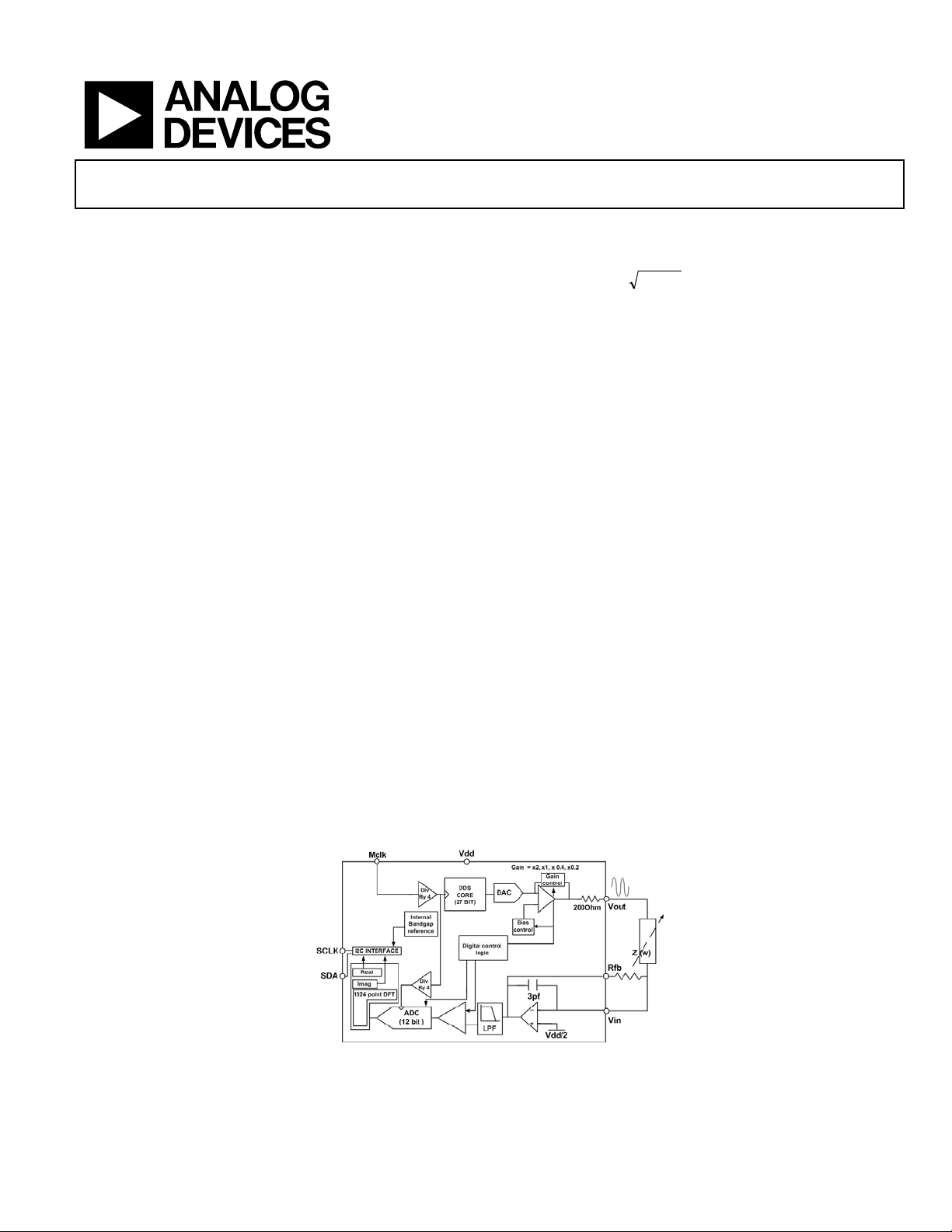
The AD5934 is a high precision impedance converter system
solution which combines an on board frequency generator with
a 12 Bit 1MSPS ADC. The frequency generator allows an
external complex impedance to be excited with a known
frequency. The response signal from the impedance is sampled
by the on board ADC and DFT processed by an on-board DSP
engine. The DFT algorithm returns a Real (R) and imaginary (I)
data word at each output frequency. This magnitude of these data
words must be further scaled by calibrated Gain Factor in order
to return the actual impedance value at each frequency point. The
magnitude of the impedance and relative phase of the
2
C loading
Network Analyzer
AD5934
impedance at each frequency point along the sweep is easily
calculated using the following equations:
122
−
)/(
=+=
To determine the value of the unknown impedance Z(w),
generally a frequency sweep is performed. The impedance can
be calculated at each point and an impedance profile i.e. frequency
vs. magnitude plot can be created. The system allows the user to
program a 2 V p-p sinusoidal signal as excitation to an external
load. Output voltage excitation ranges of 1 V, 400 mV, 200 mV
can also be programmed. The signal is provided on chip using
DDS techniques. Frequency resolution of 27 bits (less than
0.1 HZ) can be achieved using this method. To perform the
frequency sweep, the user must first program the conditions
required for the sweep; start frequency, step frequency, and
number of incremental points along the sweep into onboard
registers. Once the relevant registers have been programmed, a
Start Command to the control register is required in order to
begin the sweep. To determine the impedance of the load at any
one frequency point, Z(w), a measurement system comprised of
a transimpedance amplifier, gain stage, and ADC are used to
record data. The gain stage for the response stage is 1 or 5. At
each point on the sweep the ADC will take 1024 samples and
calculate a Discrete Fourier Transform to provide the real and
imaginary data for the response signal waveform. The real and
imaginary data stored in memory and is available to the user
through the 1
2
C interface. The ADC is a low noise; high speed
1 MSPS sampling ADC that operates from 3 V supply. Clocking
for both the DDS and ADC signals is provided externally via
the MCLK reference clock, which is provided externally from a
crystal oscillator or system clock. The AD5934 is available in a
16 lead SSOP.
RITanPhaseIRMagnitude
Figure 1. AD5934 Block Diagram
Rev. PrB
Information furnished by Analog Devices is believed to be accurate and reliable.
However, no responsibility is assumed by Analog Devices for its use, nor for any
infringements of patents or other rights of third parties that may result from its use.
Specifications subject to change without notice. No license is granted by implication
or otherwise under any patent or patent rights of Analog Devices. Trademarks and
registered trademarks are the property of their respective owners.
One Technology Way, P.O. Box 9106, Norwood, MA 02062-9106, U.S.A.
Tel: 781.329.4700 www.analog.com
Fax: 781.326.3113 © 2005 Analog Devices, Inc. All rights reserved.

AD5934 Preliminary Technical Data
TABLE OF CONTENTS
Specifications..................................................................................... 3
The Analog-to-Digital Converter ............................................ 24
Timing Characteristics..................................................................... 9
Absolute Maximum Ratings.......................................................... 10
ESD Caution................................................................................ 10
Pin Configuration and Descriptions............................................ 11
Typical Performance Characteristics........................................... 12
Terminology .................................................................................... 17
DAC/DDS core: ..........................................................................17
ADC: ............................................................................................ 18
System Architecture Description.................................................. 19
Output Stage................................................................................ 19
DDS Core: Circuit Description ................................................ 19
Numerical Controlled Oscillator.............................................. 20
SIN ROM..................................................................................... 20
Digital-to-Analog Converter & Output Gain Stage............... 20
Response Stage............................................................................ 20
The Discrete Fourier Transform .............................................. 24
AD5934 Discrete Fourier Transform Leakage ....................... 25
Gain Factor Calculation ............................................................ 27
AD5934 System Calibration ..................................................... 28
Performing a Frequency Sweep—Flow Chart............................ 31
Register Map (Each Row Equals 8 Bits of Data) ........................ 32
Control Register ......................................................................... 35
Control Register Decode........................................................... 36
Status Register:............................................................................ 36
Serial Bus Interface..................................................................... 38
General I
Writing/Reading to the AD5934.............................................. 39
Block Write.................................................................................. 41
AD5934 Read Operations ......................................................... 42
Error Correction......................................................................... 43
2
C Timing.................................................................... 38
ADC Operation ..........................................................................21
DFT Conversion......................................................................... 21
AD5934 Theory of Operation....................................................... 23
DDS Core..................................................................................... 23
Analog Channel and Filter Network........................................ 24
REVISION HISTORY
3/05—Revision PrB
Checksum.................................................................................... 43
User Command Codes .............................................................. 43
Writing to Memory: Storing Calibration Variables............... 44
Outline Dimensions....................................................................... 47
Ordering Guide .......................................................................... 47
Rev. PrB | Page 2 of 48

Preliminary Technical Data AD5934
SPECIFICATIONS
VDD = +3.0 V ±10% T
Table 1.
Y Version
Parameter Min Typ Max Unit Test Conditions/Comments
SYSTEM SPECS
Impedance Range 0.001 10 MΩ
Total System Accuracy 1 %
System ppm 250 ppm/°C Vdd = 3.3 V @ 25°C, 500 Hz bandwidth
MCLK Update Rate 16 MSPS System clock update rate
OUTPUT STAGE
FREQUENCY SPECS
Output Frequency Range 0 100 kHz Hz
Output Frequency Resoltuion 27 Bits
MCLK External Rerference Clock.
Initial Frequency Accuracy 0.1 Hz
OUTPUT VOLTAGE SPECS
AC Voltage Range (div by 1) 2.0 Volts peak to peak
Output Voltage Error 0.9 %
DC Bias (vdd/2 ) 1.65 Volts DC bias of AC Signal vdd = 3.3 V
DC Bias Error ±9 % Tolerance of DC Bias
AC Voltage Range div by 2 1.0 Volts peak to peak
Output Voltage Error 0.8 %
DC Bias (Vdd/4) 0.79 Volts DC bias of AC Signal vdd = 3.3 V
DC Bias Error ±10 % Tolerance of DC Bias
AC Voltage Range div by 5 0. 4 Volts peak to peak
Output Voltage Error 0.7 %
DC Bias (Vdd/10) 0.32 Volts DC bias of AC Signal vdd = 3.3 V
DC Bias Error ±9 % Tolerance of DC Bias
AC Voltage Range div by 10 0.2 Volts peak to peak
Output Voltage Error 0.4 %
DC Bias (Vdd/20) 0.16 Volts DC bias of AC Signal vdd = 3.3 V
DC Bias Error ±7 % Tolerance of DC Bias
DC Output Impedance
(at Vout)
DC Output Impedance 2.4 kΩ
DC Output Impedance 1 KΩ
DC Output Impedance 600 Ω
MIN
to T
unless otherwise noted.
MAX
1,2
400 Ω
Uni-Polar Sinusoidal Signal at Vout. System
accuracy only guarentted in this range.
>100 kHz achievable by device but accuracy
not guarenteed.
<0.1 Hz Resolution achievable using DDS
techniques
System Output Exitation Frequency
Accuracy using external clock/crystal post
triml. 0-100 kHz Range.
Pk-Pk Unipolar output excitation Voltage on
Vout. Vdd = 3.3 V
Voltage Error on Pk-Pk Output Excitation
voltage. Vdd = 3.3 V
Pk-Pk Unipolar output excitation Voltage on
VOut. Vdd = 3.3 V
Voltage Error on Pk-Pk Output excitation
voltage. Vdd = 3.3 V
Pk-Pk Unipolar output excitation Voltage on
Vout. Vdd = 3.3 V
Voltage Error on Pk-Pk Output excitation
voltage. Vdd = 3.3 V
Pk-Pk Unipolar output excitation Voltage on
VOut. Vdd = 3.3 V
Voltage Error on Pk-Pk Output excitation
voltage. Vdd = 3.3 V
2.0 Vp-p, Output frequency = 30 kHz
(external oscillator), vdd = 3.3 V, Ta = 25°C
1.0 Vp-p, Output frequency = 30 kHz
(external oscillator), vdd = 3.3 V, Ta = 25°C
400 mVp-p, Output frequency = 30 kHz,
(external oscillator) vdd = 3.3 V, Ta = 25°C
200 mVp-p, Output frequency = 30 kHz
(external oscillator), vdd = 3.3 V, Ta = 25°C
Rev. PrB | Page 3 of 48

AD5934 Preliminary Technical Data
Y Version
Parameter Min Typ Max Unit Test Conditions/Comments
Short Circuit Current (at Vout) ±7 mA
Short Circuit Current ±1 mA
Short Circuit Current ±2. 5 mA
Short Circuit Current ±4. .5 mA
AC CHARACTERISTICS
Signal to Noise Ratio 60 dB
Total Harmonic Distortion −52 dB
Spurious free Dynamic
Range (SFDR)
Wideband (0 to 1 MHz) 56 dB
Narrowband (± 5 kHz) 85 dB
Clock Feedthrough
(0 to 17 MHz)
SYSTEM RESPONSE STAGE
ANALOG INPUT VIN
Input Leakage Current 1 nA To Pin VIN
Input Capacitance 3.5 pF
Input Impedance 68.5G Ω
ADC ACCURACY
Resolution 12 bits
Sampling Rate 1 MSPS
Integral Nonlinearity ±1 LSB No missing Codes
Differential Nonlinearity ±1 LSB Guarentted monitonic
Offset Error ±3 LSB
Gain Error ±6 LSB
TEMPERATURE SENSOR
Accuracy ±1 °C Ta = −40 °C to 125 °C
Resolution 0.03125 °C
Auto Conversion Update Rate 1 sec Temperature measurement every 1 second
Temperature Conversion
Time
−60 dB
800 µs Vdd = 3.3 V
1,2
2.0 Vp-p, Output frequency = 30 kHz
(external oscillator), vdd = 3.3 V, Ta = 25°C
2.0 Vp-p, Output frequency = 30 kHz
(external oscillator), vdd = 3.3 V, Ta = 25°C
2.0 Vp-p, Output frequency = 30 kHz
(external oscillator), vdd = 3.3v, Ta = 25°C
2.0 Vp-p, Output frequency = 30 kHz
(external oscillator), vdd = 3.3 V, Ta = 25°C
Output excitation voltage = 30kHz, external
oscillator mclk = 16.776 MHz, Ta = 25°C
vdd = 3.3 V
Output excitation voltage = 30kHz, external
oscillator mclk = 16.776 MHz, Ta = 25°C
vdd = 3.3 V
Output excitation voltage = 30 kHz, external
oscillator mclk = 16.776 MHz, Ta = 25°C
vdd = 3.3 V
Output excitation voltage = 30 kHz, external
oscillator mclk = 16.776 MHz, Ta = 25°C
vdd = 3.3 V
Output excitation voltage = 30 kHz, external
oscillator mclk = 16.776 MHz, Ta = 25°C
vdd = 3.3 V
Pin capacitance between VouT and Gnd.
Vdd = 3.3 V, @ 25°C
Input impedance between Vout and Gnd.
vdd = 3.3 V,@ 25°C. No feedback resistor
connected.
Rev. PrB | Page 4 of 48

Preliminary Technical Data AD5934
Y Version
1,2
Parameter Min Typ Max Unit Test Conditions/Comments
LOGIC INPUTS
Vih, Input High Voltage 2.3 VDD = 3 V
Vil, Input Low Voltage 0.9 VDD = 3 V
Input Current ±4.2 µA Vdd = 3.3 V, Ta =25°C,
Input Capacitance 7 pF Vdd = 3.3 V, Ta = 25°C
POWER REQUIREMENTS
Vdd 3.3 Volts
IDD (Normal Mode) 9 mA Digital and analog supply currents
IDD (Powerdown Mode) 0.7 µA Digital and analog supply currents
1
Temperature ranges are as follows: Y version = −40°C to +125°C, typical at 25°C.
2
Guaranteed by design and characterization, not production tested.
Rev. PrB | Page 5 of 48

AD5934 Preliminary Technical Data
VDD = +5.0 V ±10% T
Table 2.
Y Version
Parameter Min Typ Max Unit Test Conditions/Comments
SYSTEM SPECS
Impedance Range 0.001 10 MΩ
Total System Accuracy 1 %
System ppm 250 ppm/°C Vdd = 5.5 V @ 25°C, 500 Hz bandwidth
MCLK Update Rate 16 MSPS System clock update rate
OUTPUT STAGE
FREQUENCY SPECS
Output Frequency Range 0 100 kHz Hz
Output Frequency
Resoltuion
MCLK External Rerference Clock.
Initial Frequency Accuracy 0.1 Hz
OUTPUT VOLTAGE SPECS
AC Voltage Range div by 1 2.0 Volts peak to peak
Output Voltage Error 0.9 %
DC Bias (vdd/2 ) 1.65 Volts DC bias of AC Signal vdd = 5.5 V
DC Bias Error ±9 % Tolerance of DC Bias
AC Voltage Range div by 2 1.0 Volts peak to peak
Output Voltage Error 0. 8 %
DC Bias (Vdd/4) 0.79 Volts DC bias of AC Signal vdd = 5.5 V
DC Bias Error ±10 % Tolerance of DC Bias
AC Voltage Range div by 5 0.4 Volts peak to peak
Output Voltage Error 0.7 %
DC Bias (Vdd/10) 0.32 Volts DC bias of AC Signal vdd = 5.5 V
DC Bias Error ±9 % Tolerance of DC Bias
AC Voltage Range div by
10
Output Voltage Error 0.4 %
DC Bias (Vdd/20) 0.16 Volts DC bias of AC Signal vdd = 5.5 V
DC Bias Error ±7 % Tolerance of DC Bias
DC Output Impedance
(at Vout)
DC Output Impedance 2.4 kΩ
DC Output Impedance 1 kΩ
DC Output Impedance 600 Ω
Short Circuit Current
(at Vout)
MIN
to T
unless otherwise noted.
MAX
1,2
27 Bits
0. 2 Volts peak to peak
400 Ω
±7 mA
Uni-Polar Sinusoidal Signal at Vout.System
accuracy only guarentted in this range. >100 kHz
achievable by device but accuracy not
guarenteed.
<0.1 Hz Resolution achievable using DDS
techniques
System Output Exitation Frequency Accuracy
using external clock/crystal post triml. 0-100 kHz
Range.
Pk-Pk Unipolar output excitation Voltage on
VOut. Vdd = 5.5 V
Voltage Error on Pk-Pk Output Excitation
voltage. Vdd = 5.5 V
Pk-Pk Unipolar output excitation Voltage on
Vout. Vdd = 5.5 V
Voltage Error on Pk-Pk Output excitation
voltage. Vdd = 5.5 V
Pk-Pk Unipolar output excitation Voltage on
Vout. Vdd = 5.5 V
Voltage Error on Pk-Pk Output excitation
voltage. Vdd = 5.5 V
Pk-Pk Unipolar output excitation Voltage on
VOut. Vdd = 5.5 V
Voltage Error on Pk-Pk Output excitation
voltage. Vdd = 5.5 V
2.0 Vp-p, Output frequency = 30 kHz (external
oscillator), vdd = 5.5 V, Ta = 25°C
1.0 Vp-p, Output frequency = 30 kHz (external
oscillator), vdd = 5.5 V, Ta = 25°C
400 mVp-p, Output frequency = 30 kHz, (external
oscillator) vdd = 5. 5 V, Ta = 25°C
200 mVp-p, Output frequency = 30 kHz (external
oscillator), vdd = 5. 5 V, Ta = 25°C
2.0 Vp-p, Output frequency = 30 kHz (external
oscillator), vdd = 5. 5 V, Ta = 25°C
Rev. PrB | Page 6 of 48

Preliminary Technical Data AD5934
Y Version
Parameter Min Typ Max Unit Test Conditions/Comments
Short Circuit Current ±1 mA
Short Circuit Current ±2.5 mA
Short Circuit Current ±4.5 mA
AC CHARACTERISTICS
Signal to Noise Ratio 60 dB
Total Harmonic Distortion −52 dB
Spurious free Dynamic
Range (SFDR)
Wideband (0 to 1 MHz) 56 dB
Narrowband (±5 kHz) 85 dB
Clock Feedthrough
(0 to 17 MHz)
SYSTEM RESPONSE STAGE
ANALOG INPUT VIN
Input Leakage Current 1 nA To Pin VIN
Input Capacitance 3.5 pF
Input Impedance 68.5G Ω
ADC ACCURACY
Resolution 12 Bits
Sampling Rate 1 MSPS
Integral Nonlinearity ±1 LSB No missing Codes
Differential Nonlinearity ±1 LSB Guaraunted monitonic
Offset Error
Gain Error
TEMPERATURE SENSOR
Accuracy ±1 °C Ta = −40°C to 125°C
Resolution 0.03125 °C
Auto Conversion Update
Rate
Temperature Conversion
Time
−60 dB
1 sec Temperature measurement every 1 sec
800 µs Vdd = 5. 5 V
1,2
2.0 Vp-p, Output frequency = 30 kHz (external
oscillator), vdd = 5. 5 V, Ta = 25°C
2.0 Vp-p, Output frequency = 30 kHz (external
oscillator), vdd = 5. 5 V, Ta = 25°C
2.0Vp-p, Output frequency = 30 kHz (external
oscillator), vdd = 5. 5 V, Ta = 25°C
Output excitation voltage = 30 kHz, external
oscillator mclk = 16.776 MHz, Ta = 25°C
vdd = 5. 5 V
Output excitation voltage = 30 kHz, external
oscillator mclk = 16.776 MHz, Ta = 25°C
vdd = 5.5 V
Output excitation voltage = 30 kHz, external
oscillator mclk = 16.776 MHz, Ta = 25°C
vdd = 5.5 V
Output excitation voltage = 30 kHz, external
oscillator mclk = 16.776 MHz, Ta = 25°C
vdd = 5.5 V
Output excitation voltage = 30 kHz, external
oscillator mclk = 16.776 MHz, Ta = 25°C
vdd = 5.5 V
Pin capacitance between VouT and Gnd = 5. 5 V
@ 25°C
Input impedance between Vout and Gnd = 5.5 V
@ 25°C. No feedback resistor connected.
Rev. PrB | Page 7 of 48

AD5934 Preliminary Technical Data
Y Version
1,2
Parameter Min Typ Max Unit Test Conditions/Comments
LOGIC INPUTS
Vih, Input High Voltage 2.3 VDD = 3 V
Vil, Input Low Voltage 0.9 VDD = 3 V
Input Current ±4.2 µA Vdd = 5. 5 V,Ta =25°C,
Input Capacitance 7 pF Vdd = 5. 5 V,Ta = 25°C
POWER REQUIREMENTS
Vdd 3.3 Volts
IDD (Normal Mode) 9 mA Digital and analog supply currents
IDD (Powerdown Mode) 0.7 µA Digital and analog supply currents
1
Temperature ranges are as follows: Y version = −40°C to +125°C, typical at 25°C.
2
Guaranteed by design and characterization, not production tested.
Rev. PrB | Page 8 of 48
Preliminary Technical Data AD5934
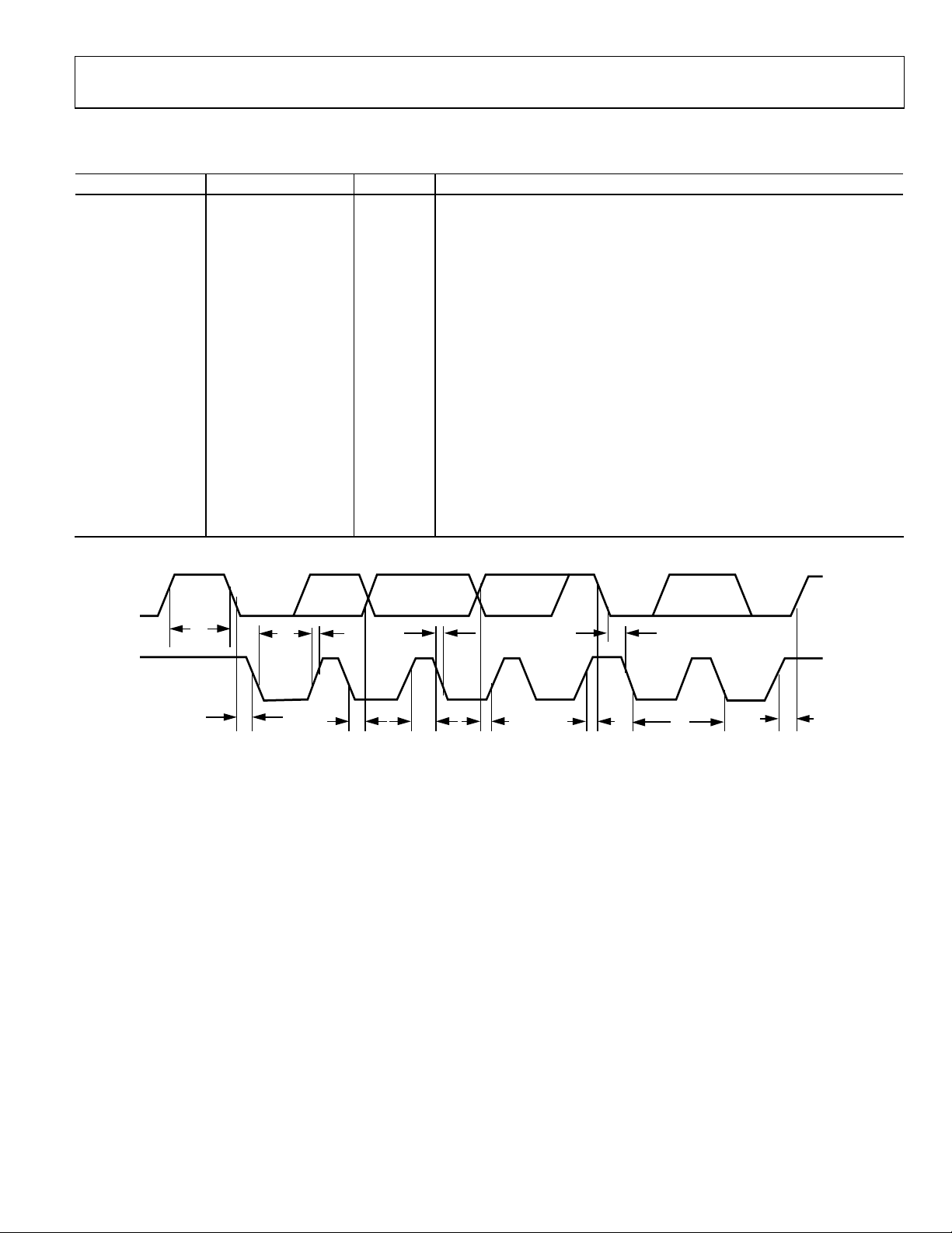
TIMING CHARACTERISTICS
Table 3. I2C Serial Interface
Parameter Limit at T
F
1483 kHz max SCL clock frequency
SCL
t1 0.7 µs min SCL cycle time
t2 0. 2 µs min t
t3 0. 6 µs min t
t4 0.6 µs min tHD,
t5 3 ns min tSU,
t6 0.9 µs max tHD,
0 µs min tHD,
t7 0.007 µs min tSU,
t8 0.6 µs min tSU,
t9 0.161 µs min t
t10 55 ns max tF, fall time of SDA when transmitting
0 ns min tR, rise time of SCL and SDA when receiving (CMOS compatible)
t11 300 ns max tF, fall time of SDA when transmitting
0 ns min tF, fall time of SDA when receiving (CMOS compatible)
300 ns max tF, fall time of SCL and SDA when receiving
20 + 0.1 CB ns min tF, fall time of SCL and SDA when transmitting
CB 400 pF max Capacitive load for each bus line
MIN
, T
Unit Description
MAX
, SCL high time
HIGH
, SCL low time
LOW
, start/repeated start condition hold time
STA
, data setup time
DAT
data hold time
DAT
data hold time
DAT
setup time for repeated start
STA
stop condition setup time
STO
, bus free time between a stop and a start condition
BUF
SDA
t
SCL
9
t
START
CONDITION
t
3
4
t
t
11
10
t
6
t
2
Figure 2. I
t
t
5
7
2
C Interface Timing Diagram
t
4
REPEATED
START
CONDITION
t
1
t
8
STOP
CONDITION
03773-0-007
Rev. PrB | Page 9 of 48

AD5934 Preliminary Technical Data
ABSOLUTE MAXIMUM RATINGS
TA = 25°C, unless otherwise note
Table 4.
Parameter Rating
VDD to GND −0.3 V to +7. 0 V
Digital Input Voltage to GND −0.3 V to VDD +0.3 V
V
to GND −0.3 V to VDD +0.3 V
OUT
Vin to GND −0.3 V to VDD +0.3 V
Operating Temperature Range
Extended Industrial (Y grade) −40°C to +125°C
Storage Temperature Range −65°C to +160°C
Maximum Junction Temperature 150°C
uSOIC Package
θJA Thermal Impedance 332°C/W
θJC Thermal Impedance 120°C/W
Lead Temperature, Soldering
Vapor Phase (60 sec) 215°C
Infrared (15 sec) 220°C
ESD 2.0 kV
Stresses above those listed under Absolute Maximum Ratings
may cause permanent damage to the device. This is a stress
rating only; functional operation of the device at these or any
other conditions above those listed in the operational sections
of this specification is not implied. Exposure to absolute
maximum rating conditions for extended periods may affect
device reliability.
ESD CAUTION
ESD (electrostatic discharge) sensitive device. Electrostatic charges as high as 4000 V readily accumulate on
the human body and test equipment and can discharge without detection. Although this product features
proprietary ESD protection circuitry, permanent damage may occur on devices subjected to high energy
electrostatic discharges. Therefore, proper ESD precautions are recommended to avoid performance
degradation or loss of functionality.
Rev. PrB | Page 10 of 48
Preliminary Technical Data AD5934
PIN CONFIGURATION AND DESCRIPTIONS
1
N/C
2
N/C
N/C
3
4
AD5934
5
VIN
VOUT
N/C
MCLK
TOP VIEW
(Not to Scale)
6
7
8
Figure 3. Pin Configuration
Table 5. Pin Function Descriptions
Mnemonic Description
N/C No Connect.
RFB_PIN External Feedback Resistor. This is used to set the gain of the input signal of the VIN node.
VOUT Input Signal to transimpedance amplifier. External Feedback resistor will control gain of transimpedance amplifier.
MCLK Master Clock for the system. Used to provide output excitation signal and as sampling of ADC.
DVDD Digital Supply Voltage
AVDD1 Analog Supply Voltage 1
AVDD2 Analog Supply Voltage 2
DGND Digital Ground
AGND1 Analog Gnd 1
AGND2 Analog Gnd 2
SDA I2C Data Input
SCL I2C Clock Input
Table 6. Recommended Pin Connections for AD5934
Mnemonic Function
Pin 1 Ext_Out Test Pin—Leave unconnected
Pin 2 NC No Connect—Do not apply any signal
Pin 3 NC No Connect—Do not apply any signal
Pin4 NC No Connect—Do not apply any signal
Pin5 Vin (Receive side of impedance) Test Impedance is connected between this pin and vout pin
Pin6 Vout (Excitation side of impedance) Test Impedance is connected between this pin and vin pin
Pin 7 NC No Connect—Do not apply any signal
Pin 8 Ext_Clk Extclk Pad—Only used if external clk option is selected
Pin 9 AVDD1 Recommended to be tied to 3.3 V
Pin10 AVDD2 Recommended to be tied to 3.3 V
Pin11 DVDD Recommended to be tied to 3.3 V
Pin12 DGND Must be tied to GND
Pin13 AGND1 Must be tied to GND
Pin14 AGND2 Must be tied to GND
Pin15 SDA I2C Data Pin
Pin16 SCL I2C Clk Pin
16
15
14
13
12
11
10
9
SCL
SDA
AGND2
AGND1RFB_PIN
DGND
AVDD2
AVDD1
DVDD
It is recommended to tie all supply connections (Pins 9, 10, 11) and run from a single supply between 3. 0 V and 5.5 V. Also, it is
recommended to connect all ground signals together (Pins 12, 13, 14).
Rev. PrB | Page 11 of 48
AD5934 Preliminary Technical Data
TYPICAL PERFORMANCE CHARACTERISTICS
1.00E-06
Ta = 25°C
Vdd = 3.3v
Rfb = 1k, 0.5k impedance
1.00E-07
1.00E-08
Gain Factor
1.00E-09
1.00E-10
0 20000 40000 60000 80000 100000
Rfb = 1k, 1k impedance
Rfb = 10k, 10k impedance
Rfb = 50k, 50k impedance
Rfb = 100k, 100k impedance
Rfb = 1M, 1M impedance
Frequency (Hz)
Figure 4. Gain Factor vs. Frequency for Various Rfb/Impedance Ranges
2.000E-08
1.980E-08
1.960E-08
1.940E-08
1.920E-08
1.900E-08
1.880E-08
Gain Factor
1.860E-08
1.840E-08
1.820E-08
1.800E-08
1.780E-08
Rfb = 1k ohm
Vdd = 3.3v
Ta = 25°C
5KΩ impedance
15KΩ impedance
10KΩ impedance
0 20000 40000 60000 80000 100000 120000
Frequency (Hz)
Figure 5. Gain Factor vs. Frequency for 5 Ωk to 15 kΩ Impedance Range
Figure 7. Gain Factor vs. Frequency for 500 kΩ to 1.5 MΩ Impedance Range
1.03E+03
1.02E+03
1.01E+03
1.00E+03
Impedance (Ohm)
9.90E+02
9.80E+02
9.70E+02
2.7V -40C
3.3V 125C
94.0E+3 96.0E+3 98.0E+3 100.0E+3 102.0E+3 104.0E+3 106.0E+3
2.7V 25C
5.5V -40C
2.7V 125C
5.5V 25C
Frequency (Hz)
3.3V -40C
5.5V 125C
3.3V 25C
Figure 8. Impedance vs. Frequency for a 1 kΩ Rfb Impedance, Gain Factor @100 kHz
2.200E-09
Rfb = 10k ohm
Vdd = 3.3v
2.180E-09
Ta = 25°C
2.160E-09
2.140E-09
2.120E-09
2.100E-09
2.080E-09
gain factor
2.060E-09
2.040E-09
2.020E-09
2.000E-09
150KΩ impedance
0 20000 40000 60000 80000 100000
100KΩ impedance
50KΩ impedance
Frequency (hz)
Figure 6. Gain Factor vs. Frequency for 50 kΩ to 150 kΩ Impedance Range
Rev. PrB | Page 12 of 48
1.03E+03
1.02E+03
1.01E+03
1.00E+03
9.90E+02
Impedance (ohms)
9.80E+02
9.70E+02
9.60E+02
54000 56000 58000 60000 62000 64000 66000
2.7V -40C
3.3V -40C
5.5V -40C
2.7V 25C
3.3V 25C
5.5V 25C
Frequency (Hz)
2.7V 125C
3.3V 125C
5.5V 125C
Figure 9. Impedance vs. Frequency for a 1 kΩ Rfb, impedance, Gain Factor @ 60 kHz
Preliminary Technical Data AD5934
0
1.03E+03
1.02E+04
1.02E+03
1.01E+03
1.00E+03
9.90E+02
Impedance ( ohm )
9.80E+02
9.70E+02
29000 31000 33000 35000 37000 39000 41000
2.7 -40C
3.3v -40C
5.5 -40C
2.7 25C
3.3 25C
5.5 25C
Frequency (Hz)
2.7 125
3.3 125C
5.5 125C
Figure 10. Impedance vs. Frequency 1 kΩ Rfb, Impedance, Gain Factor @ 35 kHz
1.03E+03
1.02E+03
1.01E+03
1.00E+03
9.90E+02
Impedance ( ohm )
9.80E+02
9.70E+02
9.60E+02
4.00E+03 6.00E+03 8.00E+03 1.00E+04 1.20E+04 1.40E+04 1.60E+04
2.7 -40
3.3 -40
5.5 25
2.7 25
3.3 25
5.5 125
Frequency (Hz)
2.7 125
5.5 -40
3.3 125
Figure 11. Impedance vs. Frequency 1 kΩ Rfb, Impedance, Gain Factor @ 10 kHz
1.01E+04
1.01E+04
1.00E+04
9.95E+03
Impedance
9.90E+03
9.85E+03
9.80E+03
54000 56000 58000 60000 62000 64000 66000
2.7V -40C
3.3V -40C
5.5V -40C
2.7V 25C
3.3V 25C
5.5V 25C
Frequency (Hz)
2.7V 125C
3.3V 125C
5.5V 125C
Figure 13. Impedance vs. Frequency 10 kΩ Rfb, Impedance, Gain Factor @ 60 kHz
1.02E+04
1.01E+04
1.01E+04
1.00E+04
9.95E+03
Impedance
9.90E+03
9.85E+03
9.80E+03
2.7V -40C
3.3V 125C
29000 31000 33000 35000 37000 39000 41000
2.7V 25C
5.5V -40C
2.7V 125C
5.5V 25C
Frequency (Hz)
3.3V -40C
5.5V 125C
3.3V 25C
Figure 14. Impedance vs. Frequency 10 kΩ Rfb, Impedance, Gain Factor @ 35 kHz
1.03E+04
1.02E+04
1.01E+04
9.95E+03
Impedance (Ohm)
9.85E+03
9.75E+03
9.65E+03
2.7V -40C 2.7V 25C 2.7V 125C 3.3V -40C 3.3V 25C
3.3V 125C 5.5V -40C 5.5V 25C 5.5V 125C
94.0E+3 96.0E+3 98.0E+3 100.0E+3 102.0E+3 104.0E+3 106.0E+3
Frequency (Hz)
Figure 12. Impedance vs. Frequency 10 kΩ Rfb, Impedance, Gain Factor @ 100 kHz
1.02E+04
1.01E+04
1.01E+04
1.00E+04
Impedance
9.95E+03
9.90E+03
9.85E+03
2.7V -40C
3.3V 125C
4500 6500 8500 10500 12500 14500 1650
2.7V 25C
5.5V -40C
2.7V 125C
5.5V 25C
Frequency (Hz)
3.3V -40C
5.5V 125C
3.3V 25C
Figure 15. Impedance vs. Frequency 10 kΩ Rfb, Impedance, Gain Factor @ 10 kHz
Rev. PrB | Page 13 of 48
AD5934 Preliminary Technical Data
0
0
0
50600
51500
50400
50200
50000
49800
Impedance
49600
49400
49200
94000 96000 98000 100000 102000 104000 106000
2.7V -40C 2. 7V 25C 2.7V 125C 3.3V -40C 3.3V 25C
3.3V 125C 5.5V -40C 5.5V 25C 5.5V 125C
Frequency
Figure 16. Impedance vs. Frequency 50 kΩ Rfb, Impedance, Gain Factor @ 100 kHz
5.06E+04
5.04E+04
5.02E+04
5.00E+04
4.98E+04
Impedance
4.96E+04
4.94E+04
4.92E+04
54000 56000 58000 60000 62000 64000 66000
2.7V -40C
3.3V -40C
5.5V -40C
2.7V 25C
3.3V 25C
5.5V 25C
Frequency (Hz)
2.7V 125C
3.3V 125C
5.5V 125C
Figure 17. Impedance vs. Frequency 50 kΩ Rfb, Impedance, Gain Factor @ 60 kHz
51000
50500
Impedance
50000
49500
49000
4000 6000 8000 10000 12000 14000 16000
2.7V -40C 2.7V 25C 2.7V 125C
3.3V -40C 3.3V 25C 3.3V 125C
5.5V -40C 5.5V 25C 5.5V 125C
Frequency (Hz)
Figure 19. Impedance vs. Frequency 50 kΩ Rfb, Impedance, Gain Factor @ 10 kHz
1.02E+05
1.02E+05
1.01E+05
1.01E+05
1.00E+05
Impedance
9.95E+04
9.90E+04
9.85E+04
9.80E+04
9.40E+04 9.60E+04 9.80E+04 1.00E+05 1.02E+05 1.04E+05 1.06E+
2.7V -40C
3.3V -40C
5.5V -40C
2.7V 25C
3.3V 25C
5.5V 25C
Frequency (Hz)
2.7V 125C
3.3V 125C
5.5V 125C
Figure 20. Impedance vs. Frequency 100 kΩ Rfb, Impedance, Gain Factor @ 100 kHz
5.05E+04
5.03E+04
5.01E+04
4.99E+04
Impedance
4.97E+04
4.95E+04
4.93E+04
29000 31000 33000 35000 37000 39000 4100
2.7V -40C
3.3V -40C
5.5V -40C
2.7V 25C
3.3V 25C
5.5V 25C
Frequency (Hz)
2.7V 125C
3.3V 125C
5.5V 125C
Figure 18. Impedance vs. Frequency 50 kΩ Rfb, Impedance, Gain Factor @ 35 kHz
1.02E+05
1.01E+05
1.01E+05
1.00E+05
Impedance
9.95E+04
9.90E+04
9.85E+04
54000 56000 58000 60000 62000 64000 660
2.7V -40C
3.3V -40C
5.5V -40C
2.7V 25C
3.3V 25C
5.5V 25C
Frequency ( Hz)
2.7V 125C
3.3V 125C
5.5V 125C
Figure 21. Impedance vs. Frequency 100 kΩ Rfb, Impedance, Gain Factor @ 60 kHz
Rev. PrB | Page 14 of 48
Preliminary Technical Data AD5934
1.02E+05
5.30E+05
1.01E+05
1.01E+05
1.00E+05
Impedance
9.95E+04
9.90E+04
9.85E+04
29000 31000 33000 35000 37000 39000 41000
2.7V -40C 2.7V 25C 2.7V 125C
3.3V -40C 3.3V 25C 3.3V 125C
5.5V -40C 5.5V 25C 5.5V 125C
Frequency (Hz)
Figure 22. Impedance vs. Frequency 100 kΩ Rfb, Impedance, Gain Factor @ 35 kHz
540000
535000
530000
525000
520000
515000
Impedance
510000
505000
500000
495000
490000
9.40E+04 9.60E+04 9.80E+04 1.00E+05 1.02E+05 1.04E+05 1.06E+05
2.7V -40C
3.3V -40C
5.5V -40C
2.7V 25C
3.3V 25C
5.5V 25C
Frequency (Hz)
2.7V 125C
3.3V 125C
5.5V 125C
Figure 23. Impedance vs. Frequency 500 kΩ Impedance, Gain Factor @ 100 kHz
5.25E+05
5.20E+05
5.15E+05
5.10E+05
Impedance
5.05E+05
5.00E+05
4.95E+05
29000 31000 33000 35000 37000 39000 41000
2.7V -40C 2.7V 25C 2.7V 125C
3.3V -40C 3.3V 25C 3.3V 125C
5.5V -40C 5.5V 25C 5.5V 125C
Frequency (Hz)
Figure 25. Impedance vs. Frequency 500 kΩ Impedance, Gain Factor @ 35 kHz
5.22E+05
5.20E+05
5.18E+05
5.16E+05
5.14E+05
5.12E+05
Impedance
5.10E+05
5.08E+05
5.06E+05
5.04E+05
5.02E+05
4500 6500 8500 10500 12500 14500 16500
2.7V -40C 2.7V 25C 2.7V 125C
3.3V -40C 3.3V 25C 3.3V 125C
5.5V -40C 5.5V 25C 5.5V 125C
Frequency (Hz)
Figure 26. Impedance vs. Frequency 500 kΩ Impedance, Gain Factor @ 10 kHz
5.35E+05
5.30E+05
5.25E+05
5.20E+05
5.15E+05
5.10E+05
Impedance
5.05E+05
5.00E+05
4.95E+05
4.90E+05
54000 56000 58000 60000 62000 64000 66000
2.7V -40C
3.3V -40C
5.5V -40C
Frequency (Hz)
2.7V 25C
3.3V 25C
5.5V 25C
2.7V 125C
3.3V 125C
5.5V 125C
Figure 24. Impedance vs. Frequency 500 kΩ Impedance, Gain Factor @ 60 kHz
Rev. PrB | Page 15 of 48
0.8
2.7V
3.3V
0.7
0.6
0.5
0.4
% Error
0.3
0.2
0.1
0
5.5V
10kHz 35kHz 60kHz 100kHz
Frequency
Figure 27. Impedance Error over 10 kHz to 100 kHz Range, Gain Factor @ 10 kHz

AD5934 Preliminary Technical Data
0.4
vdd = 3.3
Ta =25°C
Freq = 32khz
0.2
0
-0.2
-0.4
phase error (degrees)
-0.6
-0.8
-1
0 50 100 150 200 250 300 350 400
Phase (degrees)
Figure 28. Typical AD5934 Phase Error
50.1E+3
Rf = 50kΩ
impedance = 50kΩ
50.0E+3
50.0E+3
49.9E+3
49.9E+3
Impedance (Ohm)
49.8E+3
49.8E+3
49.7E+3
54.0E+3 56.0E+3 58.0E+3 60.0E+3 62.0E+3 64.0E+3 66.0E+3
vdd = 5.5v
vdd = 3.3v vdd = 2.7v
Frequency (Hz)
Figure 31. Typical Impedance e vs. Frequency for 49.992 kΩ Impedance,
Single Point Calibrated Gain Factor @ 60 kHz
3.0E+3
2.5E+3
2.0E+3
1.5E+3
1.0E+3
Impedance (Ohm)
500.0E+0
000.0E+0
k
k
k
k
P
P
V
4
.
0
k
P
P
-
-
k
k
P
V
0
2
.
.
2
0
DDS Output Voltag e Range
P
P
-
-
k
k
P
P
V
.
1
V
V
0
4
.
0
k
P
-
k
k
P
P
V
V
0
0
.
.
2
1
Vdd 3.3V Vdd 5.5V
Figure 29. Typical AD5934 Output Impedance
30.4E+3
30.4E+3
30.3E+3
30.3E+3
30.2E+3
Frequency (Hz)
30.2E+3
30.1E+3
30.1E+3
30.0E+3
vdd = 3.3
vdd = 3.3
output freq = 30khz @25°
-60 -40 -20 0 20 40 60 80 100 120 140
C
Temperature (degree C)
vdd = 5.5v
Figure 30. Typical AD5934 Frequency Temperature Coefficient
50.0E+3
50.0E+3
49.9E+3
49.9E+3
49.9E+3
49.9E+3
Impedance (ohm)
49.9E+3
49.8E+3
Rf = 50kΩ
impedance = 50kΩ
k
k
P
P
-
-
k
k
P
P
V
2
.
0
49.8E+3
49.8E+3
54.0E+3 56.0E+3 58.0E+3 60.0E+3 62.0E+3 64.0E+3 66.0E+3
vdd = 3.3v
vdd = 5.5v
vdd = 2.7v
Frequency (Hz)
Figure 32. Typical Impedance e vs. Frequency for 49.992 kΩ Impedance,
End Point Calibrated Gain Factor
Rev. PrB | Page 16 of 48

Preliminary Technical Data AD5934
TERMINOLOGY
DAC/DDS CORE:
Relative Accuracy
For the DAC, relative accuracy or Integral Nonlinearity (INL) is
a measure of the maximum deviation, in LSBs, from a straight
line passing through the endpoints of the DAC transfer
function.
Differential Nonlinearity
Differential Nonlinearity (DNL) is the difference between the
measured change and the ideal 1 LSB change between any two
adjacent codes. A specified differential nonlinearity of ±1 LSB
maximum ensures monotonicity. This DAC is guaranteed
monotonic by design.
Zero-Code Error
Zero-code error is a measure of the output error when zero
code (0000 Hex) is loaded to the DAC register. Ideally the
output should be 0 V. The zero-code error is always positive in
the AD5934 because the output of the DAC cannot go below 0
V. It is due to a combination of the offset errors in the DAC and
output amplifier. Zero-code error is expressed in mV.
Full-Scale Error
Full-scale error is a measure of the output error when full-scale
code (FFFF Hex) is loaded to the DAC register. Ideally the
output should be VDD − 1 LSB. Full-scale error is expressed in
percent of full-scale range.
Gain Error
This is a measure of the span error of the DAC. It is the
deviation in slope of the DAC transfer characteristic from ideal
expressed as a percent of the full-scale range.
Tot a l U n ad ju s te d E rr o r
Total Unadjusted Error (TUE) is a measure of the output error
taking all the various errors into account.
Zero-Code Error Drift
This is a measure of the change in zero-code error with a
change in temperature. It is expressed in µV/°C.
Gain Error Drift
This is a measure of the change in gain error with changes in
temperature. It is expressed in (ppm of full-scale range)/°C.
Digital-to-Analog Glitch Impulse
Digital-to-analog glitch impulse is the impulse injected into the
analog output when the input code in the DAC register changes
state. It is normally specified as the area of the glitch in nV secs
and is measured when the digital input code is changed by
1 LSB at the major carry transition (7FFF Hex to 8000 Hex).
Digital Feedthrough
Digital feedthrough is a measure of the impulse injected into
the analog output of the DAC from the digital inputs of the
DAC but is measured when the DAC output is not updated. It is
specified in nV secs and measured with a full-scale code change
on the data bus, i.e., from all 0s to all 1s and vice versa.
Spurious-Free Dynamic Range
Along with the frequency of interest, harmonics of the
fundamental frequency and images of these frequencies are
present at the output of a DDS device. The spurious-free
dynamic range (SFDR) refers to the largest spur or harmonic
present in the band of interest. The wideband SFDR gives the
magnitude of the largest harmonic or spur relative to the
magnitude of the fundamental frequency in the “0” to Nyquist
bandwidth. The narrow band SFDR gives the attenuation of the
largest spur or harmonic in a bandwidth of ±200 kHz about the
fundamental frequency.
Signal-to-Noise Ratio (SNR)
SNR is the ratio of the rms value of the measured output signal
to the rms sum of all other spectral components below the
Nyquist frequency. The value for SNR is expressed in decibels.
Rev. PrB | Page 17 of 48

AD5934 Preliminary Technical Data
ADC:
Integral Nonlinearity
This is the maximum deviation from a straight line passing
through the endpoints of the ADC transfer function. The
endpoints of the transfer function are zero scale, a point 1/2
LSB below the first code transition, and full scale, a point 1/2
LSB above the last code transition.
Differential Nonlinearity
This is the difference between the measured and the ideal 1 LSB
change between any two adjacent codes in the ADC.
Offset Error
This is the deviation of the first code transition (00 . . . 000) to
(00 . . . 001) from the ideal, i.e., AGND + 0.5 LSB.
Total Harmonic Distortion
Total harmonic distortion (THD) is the ratio of the rms sum of
harmonics to the fundamental. where V1 is the rms amplitude
of the fundamental and V2, V3, V4, V5 and V6 are the rms
amplitudes of the second through the sixth harmonics. For the
AD5934, it is defined as
2
2
2
2
THD
2
=
2
log20)dB(
4
3
V
1
++++
VVVVV
6
5
Gain Error
This is the deviation of the last code transition (111 . . . 110) to
(111 . . . 111) from the ideal (i.e., VREF − 1.5 LSB) after the
offset error has been adjusted out.
Signal to (Noise + Distortion) Ratio
This is the measured ratio of signal to (noise + distortion) at the
output of the A/D converter. The signal is the rms amplitude of
the fundamental. Noise is the sum of all non fundamental signals
up to half the sampling frequency (fS/2), excluding dc. The ratio is
dependent on the number of quantization levels in the digitization
process; the more levels, the smaller the quantization noise. The
theoretical signal to (noise + distortion) ratio for an ideal N-bit
converter with a sine wave input is given by
Signal to (Noise + Distortion) = (6.02N + 1.76)dB
Thus for a 12-bit converter, this is ≈74 dB.
Rev. PrB | Page 18 of 48

Preliminary Technical Data AD5934
∆=∆
SYSTEM ARCHITECTURE DESCRIPTION
The AD5934 is a high precision impedance converter system
solution which combines an on board frequency generator with a
12 Bit 1MSPS ADC. The frequency generator allows an external
complex impedance to be excited with a known frequency. The
response signal from the impedance is sampled by the on board
ADC and DFT processed by an on-board DSP engine. The DFT
algorithm returns both a Real (R) and Imaginary (I) data word at
each frequency point along the sweep. The impedance magnitude
and phase is easily calculated using the following equations:
MCLK
/2π
Figure 34.
Figure 35.
= Δt)
22
IRMagnitude +=
)/(1RITanPhase−=
To determine the actual real impedance value Z(W), generally a
frequency sweep is performed. The impedance can be
calculated at each point and a frequency vs. magnitude plot can
be created like that shown in Figure 33.
Figure 33.
The system allows the user to program a 2V PK-PK sinusoidal
signal as excitation to an external load. Output ranges of 1V,
500mV, 200mV can also be programmed. The signal is provided
on chip using DDS techniques. Frequency resolution of 27 bits
(less than 0.1HZ) can be achieved. The clock for the DDS can
be generated from an external reference clock. The following
section will describe the internal architecture of both the input
and output stages of the AD5934.
OUTPUT STAGE
The output stage of the AD5934, shown in Figure 34, provides a
constant output frequency or frequency sweep function which
has a programmable output voltage of 2/1/0.4/0.2V. The
frequency sweep sequence is preprogrammed to the onboard
RAM through the I
start the excitation sequence.
2
C interface. An I2C command is used to
DDS CORE: CIRCUIT DESCRIPTION
The AD5934 has a fully integrated Direct Digital Synthesis
(DDS) core to generate required frequencies. The block requires
a reference clock to provide digitally created sine waves up to 50
kHz. This is provided through an external reference clock,
MCLK. This clock is internally divided down by 4 to provide
the reference clock or fMCLK to the DDS.
The internal circuitry of the DDS consists of the following main
sections: a Numerical Controlled Oscillator (NCO), a Frequency
Modulator, SIN ROM, and a Digital-to-Analog Converter.
DDS Theory of Operation
Sine waves are typically thought of in terms of their magnitude
form A (t) = sin (2πft). However, these are nonlinear and not
easy to generate except through piecewise construction. On the
other hand, the angular information is linear in nature. That is,
the phase angle rotates through a fixed angle for each unit of
time. The angular rate depends on the frequency of the signal
by the traditional rate of 2πf.
Knowing that the phase of a sine wave is linear and given a
reference interval (clock period), the phase rotation for the
period can be determined.
twphase
Solving for w = Δ phase / Δ t = 2 π f
Solving for f and substituting the reference clock frequency for
the reference period (1/f
f = Δ phase x f
MCLK
Rev. PrB | Page 19 of 48

AD5934 Preliminary Technical Data
The AD5934 builds the output based on this simple equation. A
simple DDS core can implement this equation with three major
subcircuits: Numerically Controlled Oscillator + Phase Modulator,
SIN ROM, and Digital-to-Analog Converter. Each of these sub
circuits is discussed in the following section.
NUMERICAL CONTROLLED OSCILLATOR
The main component of the NCO as shown in Figure 36, is a
27-bit phase accumulator. Continuous time signals have a phase
range of 0 to 2π. Outside this range of numbers, the sinusoid
functions repeat themselves in a periodic manner. The digital
implementation is no different. The accumulator simply scales
the range of phase numbers into a multi-bit digital word. The
phase accumulator in the AD5934 is implemented with 27 bits.
Therefore in the AD5934, 2π = 2
scaled into this range of numbers:
0 < ∆ Phase < 2
27
− 1
Making these Substitutions into the equation above
f = Δ Phase × f
MCLK
/227
The input to the phase accumulator is taken from the contents
of the start frequency register (see RAM locations 82h, 83h, 84h).
Although the phase accumulator offers 27 bits of resolution the
start frequency register has the three MSBs set to zero, thus the
register only gives 24 bit frequency tune ability to the user whilst
retaining 27 bit resolution therefore the minimum clock frequency
which can be used for the AD5934 to retain system accuracy
is ≈ 500 kHz.
27
, Likewise, the ∆Phase term is
This requires the SIN ROM to have two bits of phase resolution
more than the 9-bit DAC.
DIGITAL-TO-ANALOG CONVERTER & OUTPUT GAIN STAGE
The DDS includes a high impedance current source 9-bit DAC.
The output from the DAC is a current (0 − 2 ma, this is ratiometric with the supply voltage), so in order to develop a current
the output current is passed through a precision grounded load
resistor such that the output will be a sinusoid voltage. This
voltage is subsequently delivered to an inverting gain stage gain
stage as shown in Figure 37. The output voltage amplitude from
the DAC may be set to a value of 2 V p-p, 1 V p-p, 400 mV p-p
or 200mv p-p depending upon the state of switches on the
feedback path of the amplifier. Only one switch will be closed at
any time. The output voltage amplitude can be programmed by
setting bits D10 and D9 in the control register. (See control
register section for further details).The output bias voltage of
the excitation voltage will also vary depending upon the value
of the excitation voltage amplitude set by the user as is
summarized in Table 7. The DC bias level is ratio metric with
respect to the supply voltage to the AD5934
Figure 36.
SIN ROM
To make the output from the NCO useful, it must be converted
from phase information into a sinusoidal value. Since phase
information maps directly into amplitude, the SIN ROM uses
the digital phase information as an address to a look-up table,
and converts the phase information into amplitude. Although
the NCO contains a 27-bit phase accumulator, the output of the
NCO is truncated to 12 bits. Using the full resolution of the
phase accumulator is impractical and unnecessary as this would
require a look-up table of 2
sufficient phase resolution such that the errors due to
truncation are smaller than the resolution of the 9-bit DAC.
27
entries. It is necessary only to have
Rev. PrB | Page 20 of 48
Figure 37.
Table 7.
Output Excitation Voltage
Amplitude Output DC Bias Level
2vp-p 1.6 V (vdd/2)
1vp-p 0.8 V (vdd/4)
400mv p-p 0.32 V (vdd/10)
200mv p-p 0.16 V (vdd/20)
RESPONSE STAGE
The diagram in Figure 38 shows the input stage to pin VOUT.
Current from the external sensor/unknown impedance/ load
flows through the VOUT pin and into a trans-impedance
amplifier which has a user determined external resistor across
its feedback path. The feedback resistor is connected between
pin 4 and pin 5. The user needs to choose a precision resistor in
the feedback loop such that the dynamic range of the ADC is
used and that the response signal resides within the linear range
of the ADC whilst ensuring the gain factor variation over the
impedance and frequency range of interest is minimized. The

Preliminary Technical Data AD5934
positive node of the Trans-impedance amplifier and gain
amplifier are biased at a fixed value of VDD/2. The output of
the Trans-impedance amplifier can then be gained by either 1
or 5, and is fed directly into the input of the ADC. The value of
this pre-ADC gain is determined by the status of bit D8 in the
control register.
Figure 38.
ADC OPERATION
The AD5934 has an integrated on board 12 bit ADC. The ADC
contains an on-chip track and hold amplifier, a successive
approximation A/D converter. Clocking for the A/D is provided
using a divided down ratio of the reference clock.
The A/D is a successive approximation analog to digital
converter, based on a Capacitive DAC design Architecture.
Figure 39 shows a simplified schematics of the ADC. The ADC
is comprised of control logic, a SAR, and a capacitive DAC, all
of which are used to add and subtract fixed amounts of charge
from the Sampling capacitor to bring the comparator back into
a balanced condition. Figure 39 shows the ADC during its
acquisition phase. SW2 is closed and SW1 is in position A, the
comparator is held in a balanced condition, and the sampling
capacitor acquires the signal on ADC input pin.
comparator to become unbalanced. The control logic and the
capacitive DAC are used to add and subtract fixed amounts of
charge from the sampling capacitor to bring the comparator
back into a balanced condition. When the comparator is
rebalanced, the conversion is complete. The control logic
generates the ADC output code.
Figure 40.
The start conversion (CS ) for the ADC is controlled via an
internal gated signal which provides the delay from the start of
the excitation signal to the time from which the ADC starts
converting the response signal. The gate enable signal is
determined by the status of the reset bit, update frequency bit
start frequency sweep bit of the control register (80h, 81h).The
delay between the time the DDS core outputs the current
excitation signal and the time the ADC starts converting the
response signal is determined by the value programmed into
the “settling time cycles” register and the inherent
multiplication factor which maybe performed on this register
contents (see ram location 8Ah, 8Bh). The data from the ADC
is directly made available to a window coefficient generator
prior to being passed to the DSP core of the AD5934 which
performs a dft on this windowed sampled data.
Figure 39.
When the ADC starts a conversion, SW2 will open and SW1
will move to position B, as shown in Figure 40, causing the
DFT CONVERSION
A discrete Fourier transform is calculated for each frequency
point in the sweep. The return signal is converted by the ADC,
windowed and then multiplied with a test phasor value to give a
real and imaginary output. This is repeated for 1024 sample
points of the input signal and the results of each multiplication
summed to give a final answer as a complex number. The
resultant answer at each frequency is two 16 bit words, the real
and imaginary data in complex form.
Rev. PrB | Page 21 of 48

AD5934 Preliminary Technical Data
Prior to performing a sweep the user will need to calibrate the
system in order to set the Correct output voltage excitation
value, external feedback resistor and pre-ADC voltage gain
setting in order to place the response signal in the linear range
of the ADC and more importantly such that GAIN FACTOR
returned by the setting is accurate. The user calculates this
GAIN FACTOR value from the real and imaginary components
returned from the device when the calibration impedance is
between Vin and Vout.
Figure 41.
The DFT algorithm is represented by
1023
()
∑
n
=
0
−=
))sin())(cos(()(
njnnxfX
Where X (f) is the frequency component corresponding to
windowed response sample x (n). The details of the dft
conversion are explained in detail in the section:AD5934:
theory of operation. Both the real and imaginary data register
have 15 bits of data and one sign bit. The 15 bits of data are in
twos compliment format. The magnitude of the response signal
after each conversion can be calculated by the real and
2
imaginary components returned through the I
22
IRMagnitude +=
C interface
factorGain
=
Z
NCALIBRATIO
22
IR
+
Where Z
CALIBRATION
is a known precision impedance (e.g.
precision resistor) value .R and I are the real and imaginary
components returned from the AD5934 which has been
previously calibrated to set the various gain, bias settings, and
external feedback value.
The real and imaginary components
are stored at location 94h to 97h (see register map)
The calibration impedance should be chosen such that the
known impedance lies within the middle of the unknown
impedance range. The calibration should be carried out at
frequency point which lies in the mid frequency band of
interest. The calibration should also be carried out at a
temperature which lies in the mid temperature range of interest.
The gain factor returned may be subsequently used to
recursively calibrate the system. The results returned by the
AD5934 may be improved upon by carrying out a two point
calibration. System calibration and the calculation of the gain
factor is explained in more detail in section: Gain factor
calculation, system calibration.
This magnitude which is must be calculated off chip is a scaled
valued of the actual impedance being measured between Vout
and Vin. The multiplication factor between the magnitude
returned and the actual impedance value is called the GAIN
FACTOR.
Rev. PrB | Page 22 of 48

Preliminary Technical Data AD5934
AD5934 THEORY OF OPERATION
Figure 42. AD5934 Block Overview
DDS CORE
The DDS allows for a 0.1 Hz resolution frequency output which
the user can program via a 24 bit word, loaded serially over the
2
C interface. The word loaded is the result of a simple formula
I
shown in equation 1, based on the master clock frequency and
the desired frequency output of the DDS.
)1(
Eqn
⎧
⎛
⎜
⎪
⎪
coderequired
⎜
=
⎨
⎜
⎪
⎜
⎪
⎝
⎩
⎛
⎜
⎝
Mclk
4
FrequencyOutputDDS
⎞
⎟
⎠
⎫
⎞
⎟
⎪
⎪
27
⎟
2
×
⎬
⎟
⎪
⎟
⎪
⎠
⎭
In addition the DDS provides both the sin and cosine
coefficients for the DFT operation. These coefficients are
applied to the Multiply/Accumulate (MAC) blocks on every
rising edge of the system clock. One of the generated sinusoids
is simultaneously converted into a voltage waveform by passing
the output of the phase accumulator core to a high impedance
output current DAC with a precision load resistor to ground on
the output.The output of the DDS/DAC is a current from 0 to
2 mA. This current is passed through a grounded precision
resistor such that maximum voltage by default is ±2 V peak to
peak. This voltage is applied to the VOUT pin. There is the
provision for dividing down this voltage as the application
requires. By writing to the control register, the user can set this
voltage applied to VOUT to be a divide by 10, 5 or 2 (200mV pp, 400mVp-p, 1Vp-p by setting bits D10, D9 of the control
register. The DC bias level changes on the output excitation
voltage will change according to the selected output amplitude
value programmed as shown in Figure 43.
Figure 43. Output Excitation Voltage Levels and Bias Values
The DDS can be programmed with a start frequency, a
frequency increment, a delay to allow a complex impedance
system to settle and the ability to repeat the same frequency
point multiple times (for example in the event of an interface
error).The complex impedance network to be excited by the
DDS output voltage is connected between VOUT (pin 6) and
VIN (Pin 5).
Rev. PrB | Page 23 of 48

AD5934 Preliminary Technical Data
ANALOG CHANNEL AND FILTER NETWORK
The output of the complex impedance network is applied to
VIN (pin 5).This is the input node to an Trans impedance
amplifier with a feedback resistance determined by the user
Rfb—thus the gain of this first amplifier is Rfb/Z(w), where
Z(w) is the value of the impedance under test, for example, if
the value of Rfb
is chosen to be 200 kΩ and the value of the
complex impedance at a given frequency say 100 kHz is 1MΩ,
then this first amplification stage would be an attenuation of
0.2. The second stage of amplification can be either a gain of 1
or a gain of 5. The gain of 5 would correct the above mentioned
attenuation, the gain of one is necessary when large impedances
between Vout and Vin are to be measured, as the signal into the
ADC has to be controlled so as not to go outside its dynamic
range. The gain of 5 and gain of 1 is user programmed via bit
D8 of the control register. After the gain stage the signal is
buffered and has to settle a pre ADC sampling cap (~12p) to
12 bits within 180 ns) and filtered before it is applied to the
12-bit SAR ADC. Filter poles have been designed into the
channel to roll of noise. In addition to this, the subsequent DFT
operation narrows bands noise to −3 dB at freq ±1 kHz (2 kHz
noise band width) around the DDS output drive frequency, due
to an integrated hanning window function (see dft and
windowing).
THE ANALOG-TO-DIGITAL CONVERTER
The function of the ADC is to implement the digitization of the
return signal from the complex network for use with DFT. The
ADC samples the return signal at 1 MHz, and provides the
samples to the digital engine. The details of the ADC are
explained in the section: system architecture description.
THE DISCRETE FOURIER TRANSFORM
The AD5934 method of determining the amplitude of the
sensor/impedance network signal involves the use of the DFT.
The DFT is a purely digital approximation of the Continuous
Fourier Transform. It takes a number N, of samples from a time
domain signal (the sine-wave in this case x(t)) and returns the
spectral content of that signal as a complex number R + jI.
These complex numbers describe the x (t). The DFT offers
excellent dc rejection, an averaging of errors and provides the
phase information. The AD5934 implemented DFT assumes
that a sequence of periodic data samples x(n) of which we wish
to determine the spectral content of the original continuous
excitation signal on Vout. These samples come from the 12-bit
ADC which has the complex impedance/sensor signal as its
input, for a range of signal-frequency values. The method
employed differs from the conventional DFT, in that only a
single frequency bin is transformed, rather than a fundamental
and its harmonics—it’s a single-point DFT.
With the conventional DFT, a sequence of input samples is
correlated with samples from a phasor. The frequency of this
phasor is at integer multiples of a fundamental frequency given
by fs/N. The correlation is performed for each frequency
multiple, if the resulting correlation of the phasor (consisting of
both a sine and a cosine at that multiple frequency) is non-zero,
then we can deduce that there is energy in the input signal at
that particular frequency bin. (Dividing the frequency axis into
n, equally spaced analysis phasor-bins is common in DFT
analysis). If no energy is found in a bin then there can be no
energy at that test frequency. With the single-point DFT the
analysis frequency is always the same as the input frequency (by
design), we are only looking for energy at one particular
frequency. So we only perform the DFT for one frequency bin,
which is fixed for the particular input frequency.
For example, if the complex impedance is excited with a 27 kHz
sinusoid, then the output of the complex impedance is sampled
and quantized. The resulting sample values are then used as the
input values to the DFT, which uses an analysis frequency (from
the DDS) also at 27K HZ. What this effectively does is correlate
the output voltage samples with the test phasor. For a coherent
system this will give us back exactly the correct answer in the
form of a single complex number (R + jI).
In rectangular or trigonometric form, the DFT has the form
shown in Equation 1.
)2(
−
1
N
⎛
nxmX
=
∑
⎜
⎝
=
0
n
mn
2
π
cos()()(
N
2
j
sin()
−
Eqn
mn
π
⎞
)
⎟
N
⎠
where:
th
X(m) is the m
DFT output, corresponding to the complex
output for that input sample.
m is the index of the DFT outputs component in the frequency
domain.
n is the time-domain index of the input samples—both n, m
0,1,2...N-1
N is the number of samples in the input sequence that will be
transformed to the frequency domain, and the number of
frequency points in the DFT output.
x(n) is the discrete sequence of time-domain sampled values of
the continuous waveform. (The ADC output in this
application),The number of points taken for the DFT, that is,
the DFT length N is an important number, it determines both
the accuracy of the final result and the complexity of the
circuitry required to calculate the results.
To highlight the dft with an example, assume the following
values.
• Sampling Frequency = 1 MHz = Fs
• N = 1024
• Input Signal = A sin (2πft+Ø)
• A = 1, f = 27k to 32k, t = 1/Fs, Ø = 0
Rev. PrB | Page 24 of 48

Preliminary Technical Data AD5934
N
The conventional DFT returns the spectral content at discrete
frequency bins given by Fs/N = roughly every 1 kHz in this
case. For N input (time-domain) samples the DFT will return N
frequency-domain results in complex - or rectangular form, a
real and an imaginary component. The simplified sequence of
events that results in a DFT is as follows.
1.
DDS outputs a single frequency of amplitude A and phase
Ø .
2.
For each value output from the DDS (A sin (2fπn/N)),
where n = 0 … N-1, the DDS also passes the cos and sin of
this value to the DFT multiply and Accumulator block
(MAC).
3.
The MACs (one for both the sin and cos) will multiply the
values passed by the DDS with the sampled values returned
from the sensor/network (which has been multiplied with
a hanning window function—see below for further details)
4.
This is repeated for N samples.
5.
After N cycles the values in the MACs contain the digital
equivalent of the real (cos*x(t)) and imaginary (sin*x(t)),
DFT output values. This is essentially a correlation of the
response signal with the current DDS output waveform.
6.
These values are transmitted to the off-chip by the user to a
microcontroller where the real and imaginary components
are conditioned into an impedance of the sensor/
impedance network for that particular frequency.
7.
The process is repeated for point along the frequency
sweep range conditions programmed into the AD5934
RAM (see section on AD5934 registers for further details)
Subsequently the microcontroller will process the data returned
from AD5934 for each sweep point to extract the Impedance.
AD5934 DISCRETE FOURIER TRANSFORM LEAKAGE
Leakage causes the DFT results to be only an approximation of
the true spectra of the original input signal. DFTs are
constrained to operate on a finite set of N input values sampled
at a sample rate of Fs, to produce an N-point transform whose
discrete outputs are associated with the individual analytical
frequencies, that are integer multiples of (m*Fs)/N. The
problem is that the DFT only produces correct results when the
input data sequence contains energy precisely at the analysis
frequencies that are integral multiples of the fundamental
frequency. If the input signal has a component at some
intermediate frequency between these frequency bins, this input
signal will show up to some degree in all of the N output
frequency bins of the DFT. In a conventional DFT this can have
the undesirable effect of masking out weaker signals that are
present close to stronger ones in the input signal.
Leakage is caused by the discontinuities caused by the DFT
assuming a periodic input signal. If the input signal does not
have an exact integral number of cycles over the N-point sample
interval then we will not have a smooth transition from the end
of one period to the start of the next. Firstly the very fact that a
finite number of points have been sampled to form the DFT, we
are in effect multiplying the input sequence by a rectangular
window of an assumed infinite signal in the time domain. The
CFT of a rectangular function is the sinc function (which we
approximate with the DFT), and if the input signal contains
components at exactly integer multiples of the fundamental
analysis frequency, then these side lobes will be zero at bin
frequencies and will not show up in the DFT output. If however,
the input signal contains components that do not fall exactly on
these bin frequencies, then the sinc functions side lobes will
contain energy at the bin frequencies. It is the high-frequency
components inherent in the discontinuities of non-periodic
sampling that causes these side lobes to exist.
In the single-point DFT that the AD5934 is concerned with, the
sampling frequency for this is set at 1 MHz, and N =1024. This
gives bin frequencies at integer multiples of ~1 kHz. So if we
wanted accurate DFT outputs, the input signal would be
restricted to 1 kHz multiples – the resolution of the DFT is said
to be 1 kHz, i.e., the DFT will only give the correct results for
these frequencies locations. Because for the AD5934 the input
signal can take on any value, the leakage effects must be
considered
The most popular method for reducing the effects of spectral
leakage is windowing. Windowing has the effect of reducing the
energy contained in the side lobes of the sinc function. When
the input signal does not contain an integer number of cycles
within the sample interval we will have leakage as described
above. AD5934 Applications may have the additional problem
of a non-periodic analysis frequency. A conventional DFT is
performed with analysis phasors that are multiples of the
fundamental bin frequency given by Fs/N. Because the AD5934
is only performing a single-point DFTs, this is no longer the
case. The analysis phasors are not periodic between binfrequencies. In addition we also end up with cosine and sine
squared function when building up the DFT results. The result
of this is the unusual ripple that is seen on the output values
between bin frequencies. Windowing will reduce these effects
considerably.
The AD5934 uses the Hanning window to achieve the system
accuracy The Hanning window equation is an inverted, raised
cosine of half-unit amplitude peak to peak as shown in Equation 3.
...2
nf
1
)(
Where f = the sampling interval and, n = 0…N-1, and N = DFT
length.
×−=
212
π
(
CosnHanning
)3.(
Eqn
)
Rev. PrB | Page 25 of 48

AD5934 Preliminary Technical Data
The Hanning window offers good side lobe rejection and due to
its symmetrical properties is efficient to implement in a digital
engine. The window function will reduce the discontinuities at
the end of the sampling interval period and the start of the next
period (in the time domain), and forces the input time sequence
at both the beginning and end of the sample interval to go
smoothly towards a single common amplitude value. As the
output of the DFT is periodic, the periods will line up better,
with less of a transition from the last sample value to the first
sample of the next period resulting in less energy in the side
lobes of the sinc function.
Hanning Windows also have the effect of reducing the timedomain signal levels applied to the DFT; as such the main lobe
peak values are reduced (−13 dB) relative to the unwindowed
input data sequence. This leads to a predictable processing loss
that must be accounted for (with a multiplier value) when
computing the windowed DFT output values. Windowing in
the conventional sense will also widen the main lobe width,
reducing the resolution of the data, leakage effects are reduced,
but this doesn’t become a problem for AD5934 single-point
DFT.
The input data samples from the ADC are windowed, that is,
they are multiplied by a set of coefficients that are calculated
from the window function on a point for point basis. The data
samples take on the tapered profile of the window. In hardware
terms this is performed in the digital engine (just a multiplier of
sufficient bit width). The actual DFT operation must then be
done – the windowed samples are point for point multiplied
with both the sin and cosine values from the DDS and a
multiply and accumulate operation is performed in the digital
engine to give us the DFT result.
)4(
1
N
−
()(){}
∑
0
n
=
Eqn
)()cos()()()(
nxnnxnSinfX
×+×=
For N values where N=1024.
The above general equation outlines what is done on each data
sample where f is the test frequency.
Rev. PrB | Page 26 of 48

Preliminary Technical Data AD5934
e
GAIN FACTOR CALCULATION
The AD5934 device is capable of measuring impedances values
to within 1% for impedances which lie within the range of 100Ω
to 10MΩ.The DFT of the response signal from the unknown
impedance will return both a 16 bit twos complement real and
an imaginary word for each frequency point on the sweep. Each
of the data components is stored in a single 16 bit register
location (see register map).The user must read these values to
an off chip microprocessor/DSP through the I
order to calculate the impedance value at each point. The user
must poll the status register to see when there is valid data
available to read and finally to check if the entire frequency
sweep has been completed. Once valid data has become
available the user must read the current contents of the real and
imaginary data register before the next frequency sweep point
has updated the current contents with new valid data.
The magnitude of the real and the imaginary data contents each
frequency point is given by the following
22
)( IRfMagnitude +=
Where R and I correspond to the real and imaginary code
returned for the current sweep point.
This magnitude value is equal to a scaled value of the actual
impedance under test at the frequency point f. In order to
determine actual impedance value the user must multiply the
magnitude by a Gain Factor GF(freq, Vdd, temp).There fore the
actual impedance any sample instant is given by the following
2
C interface in
of the code returned by the DFT at a single frequency chosen
and by the user. This constitutes a single point gain factor
calibration. The Gain Factor is measured at a particular
frequency in the mid range of the frequency of interest. The
calibration impedance should be chosen by the user to lie in the
middle of the unknown impedance range and also in the
middle of the temperature range of interest. The gain factor
essentially is a number representing the accumulative gain
through the signal path of the system for know measured
calibration impedance and for a specified value of output
voltage excitation value and frequency/pre ADC gain setting
and feedback resistor chosen by the user. Therefore the Gain
factor will depend upon the frequency point at which it is
calculated, the AD5934 supply voltage, as the output bias level is
ratio metric with respect to the supply Vdd (see Table 7), the
device temperature as the gain of the Internal operational
amplifiers will drift with temperature, the value of the external
feedback resistor will set the gain given by |rfb/Z calibration|) of
the trans-impedance Amplifier and so effect the value of the
system gain.
As all the gains of the system are located on the signal path and
so any adjustment to the supply voltage, calibration frequency,
output excitation level, external feedback resistance value, and
pre-ADC voltage gain will require a recalculation of the Gain
factor. If the gain factor is not recalculated after any system gain
parameter adjustment then the Impedance value returned by
the AD5934 will have an error associated with it. Therefore the
accuracy of the end result will depend upon the value of the
gain factor.
×=
)()(Im fMagnitudeFactorGainfpedance
The Gain Factor is measured using a known external
impedance, e.g., a precision resistor, connected between Vout
and Vin as close as possible to the pins. Calculating the gain
factor in this way calibrates out the parasitic impedance
between Vout and Vin at a given frequency. The parasitic
impedance is made up of a parallel capacitance between Vout
and Vin as well as a series resistance and series inductance
mainly due to the bond wires and solder joints. The value of the
known calibration impedance e.g. precision resistor is measured
prior to connecting between Vout and Vin. This value acts as
the reference for calculating the gain factor. The gain factor is
given by the following formula
1
Calibrated
Admittance
)( ==fFactorGain
Code
R Code I+=
22
Impedanc
Code
The gain factor is an Admittance per code value. It is
mathematically calculated by dividing the known measured
Calibration impedance between Vout and Vin by the Magnitude
The gain factor is calculated at a single frequency in the middle
of the frequency range of interest at a known supply and
temperature after the system has been calibrated i.e. set the
correct output excitation voltage, frequency, pre ADC gain
value and correct rfb value for the impedance range under test.
The gain factor will vary in a linearly fashion as the sweep
deviates from the point at which the gain factor was calibrated,
provided the other system gain parameters remain constant i.e.
temperature, supply, feedback resistor etc .A typical gain factor
vs. frequency plot is shown in Figure 8 for various values of
impedance and feedback resistors. The frequency point at
which the gain factor was calculated will return an impedance
value with zero error provided the system has been correctly
calibrated i.e. setting the correct output excitation voltage, pre
ADC gain value and external feedback resistor. The gain factor
deviates linearly with frequency; the subsequent error in the
impedance values returned by the AD5934, introduced by the
deviation from the calibration point frequency will vary in the
same linear fashion.
If however the user performs a frequency sweep to determine
the impedance profile of the network under test / sensor using a
calibrated gain factor calculated in the middle of the frequency
Rev. PrB | Page 27 of 48

AD5934 Preliminary Technical Data
and temperature range of interest as recommended i.e.
performs a frequency sweep using a calibrated single point gain
factor, the absolute error returned by the AD5934 as the
frequency moves from the calibration frequency point can be
reduced by performing a two point calibration. Figure 4 shows
that the Gain Factor variation over frequency is approximately
linear. Thus another frequency dependant term may be used to
correct for the impedance error as follows.
GFfGFfGF
∆+= )()(
mid
GF(f) = Frequency Corrected Gain Factor
) = Gain Factor measured at mid range frequency
GF(f
ref
ΔGF = Change in Gain Factor per 1Hz change in frequency
ΔGF may be calculated from slop of the GF V’s frequency
profile. The impedance may then be recalculated using the
corrected Gain Factor as follows.
fZ
=
)(
1
)())()((
fffGFfGF
−×∆+
midmid
)()(
ffGFfGF −×∆=∆
mid
Figure 32 shows the improvement achieved in accuracy due to
frequency independent Gain Factor.
The gain factor varies with temperature; therefore the system
accuracy will vary with Device temperature. A typical
impedance vs. temperature plot is shown in Figure 9. The gain
factor will also vary with the supply voltage due to the fact that
the peak to peak excitation voltage and the output bias levels are
ratio metric with respect to supply.
AD5934 SYSTEM CALIBRATION
The gain factor (explained above) essentially is a number
representing the accumulative gain through the signal path of
the system for known calibration impedance for a specified
value of output gain voltage/pre ADC gain and feedback resistor
settings. By calibrating the device with a value of known
impedance connected between Vout and Vin you are
associating the digital output code of the AD5934 with this
known impedance value. By calibrating the system with this
known impedance you are also inherently calibrating for the
internal system gains along the system signal path. The gain
factor calculated (see section: gain factor calculation) from the
resulting code returned at a mid frequency calibration point of
interest will allow you to calculate the impedance value of the
network under test to less that 1% within an impedance range
of 5kΩ on either side of the calibration value. The resultant
absolute error returned from using this single point gain factor
as the sweep frequency deviates from the calibration point can
be reduced further as a result of carrying out a two point
calibration (see: gain factor calculation for more details).
Figure 44. Typical Gain Factor Variation for Various rfb/Z Unknown
Impedance Ranges
The gain factor is dependant upon the ratio of the transimpedance feedback resistance value RFB to the impedance
under test (Z_unknown). The shape of this variation is shown
in Figure 44. When calibrating the system the values of the
feedback resistance should be chosen such that ratio
Rfb/Z_unknown lies with in the flat region of the characteristic
marked by a red ellipse in Figure 44. In order for the AD5934 to
return accurate values, it is necessary to ensure that the largest
signal is returned to the ADC whist ensuring that gain factor
will not vary significantly over the unknown impedance range.
Minimising the gain factor variation is achieved by placing the
AD5934 operating point in this flat region as indicated in
Figure 44 in this flat region the variation of the gain factor for
the unknown impedance range will be minimised. The ratio of
feedback resistor to Calibration impedance should lie in the
range of 0.2, 0.1 and 0.066 shown as points A, B and C in Figure
44. in The output excitation voltage is programmable to be 2 V,
1 V, 400 mV and 200mv p-p dependant upon bits D10 and D9
of the control register as explained earlier (See Control register,
system Architecture for more details). The response signal can
be subsequently amplified by a factor of x1 or x5 dependant
upon the state of bit D8 of the control register. The output
excitation voltage setting and Pre-ADC gain should be chose
such that the largest signal is presented to the ADC input whilst
ensuring that the Gain factor dose not vary significantly as
outlined in the last paragraph.
There fore in order to calibrate the AD5934 the user must know
in what impedance range (±10KΩ) the unknown impedance
connected between Vout and Vin lies. The user subsequently is
required to choose a known measured calibration impedance
e.g. 1% precision resistor, which lies in the middle of this user
determined impedance range. This calibration resistor is chose
such that the ratio of Rfb /Zcal-mid lies within the range of (0.2,
0.1, 0.066). The upper limit of Rfb within the unknown
Rev. PrB | Page 28 of 48

Preliminary Technical Data AD5934
g
impedance range therefore should be no more that Zcal-mid x
0.2 and no less than (Zcal-mid x 0.066). The output voltage
excitation levels and pre ADC settings are then chosen such that
the largest signal is then presented to the ADC input (≈ 2vp-p)
by choosing a output excitation voltage of 2vp-p and a pre ADC
gain of 5.A sample matrix of such system settings is shown in
Table 8 for a variation of chosen impedance values.
Table 8. AD5934 System Conditions
Output
Impedance
Range (Ω)
Rfb
Value
(Ω)
Excitation/
Pre-ADC
Settings
5k to 15k 1k 2vp-p, x5 5k, 10k, 15k
Chosen
Impedance
Values
Rfb/
Z_unknown
Ratio
0.2, 0.1,
0.066
50k to 150k 10k 2vp-p, x5
500k to
100k 2vp-p, x5
1.5M
1M to 3M 200k 2vp-p, x5 1M, 2M, 3M
50k, 100k,
150k
500k, 1M,
1.5M
0.2, 0.1,
0.066
0.2, 0.1,
0.066
0.2, 0.1,
0.066
Example: Taking the case where the unknown impedance
connected between Vout and Vin of the AD5934 is known to lie
between 50kΩ and 150kΩ impedance range and the user would
like to analyze the unknown impedance profile of the network
under test within the 10 kHz to 120 kHz frequency range. The
user will then choose a calibration impedance which lies in the
middle of this impedance range, i.e., 100 kΩ. The user must
then choose a value of feedback resistor so suit the impedance
range and ensure the gain factor variation within this known
impedance range is limited to lie within (0.2 < 0.1 <
0.066).Therefore a 1 kΩ resistor is chosen by the user.
In order to ensure that the gain factor did not in fact vary over
the impedance range for the chosen value of feedback resistance
the user takes a known impedance value from the start middle
and end of the impedance range e.g. 50kΩ, 100kΩ and 150KΩ
.The user calibrates the system using each of the sample
impedances in turn, at a mid frequency point of interest i.e.
60 kHz and at a mid point temperature of interest e.g. 25°C. In
each case the user selects the output excitation voltage to be
2vp-p and the pre-ADC gain value to be x5 to get the largest
signal to the ADC over the impedance range. The digital code
Returned at each point in the frequency range of interest (10
kHz-120 kHz) was then used to calculate a Gain factor. The
variation in the gain factor versus frequency is shown below in
Figure 45.
2.200000E-09
2.180000E-09
2.160000E-09
2.140000E-09
2.120000E-09
2.100000E-09
ain factor
2.080000E-09
2.060000E-09
2.040000E-09
2.020000E-09
2.000000E-09
Figure 45. Calibrated Gain Factor vs. Sweep Frequency for a Feedback
0.5
0.4
0.3
0.2
0.1
% E rro r
0
-0.1
-0.2
-0.3
150KΩ impedance
0 20000 40000 60000 80000 100000
Resistor of 10 kΩ over Unknown Impedance Range
1.0E+0 2.0E+0 3.0E+0 4.0E+0
Figure 46. Impedance Range Error
100KΩ impedance
measurement frequency (hz)
Impedance Range Error
Measurement Frequency (Hz)
Gain ratio = 0.2
50KΩ impedance
Gain ratio = 0.066
Total error
Figure 46 shows the impedance range % error versus frequency
from a known calibration impedance of 100kΩ calibrated at
60 kHz. The plot shows that the % error is < 1% - with the
smallest error being returned at the calibration frequency in
accordance with the gain factor theory. The plot also shows, as a
result of the reducing the gain factor variation over the
impedance range, the variation in the error returned by the
AD5934 over frequency is subsequently reduced to < 0.2%.
Rev. PrB | Page 29 of 48

AD5934 Preliminary Technical Data
Summary of calibration steps
• The user must establish in what range the impedance
under analysis lies and what frequency range the
impedance needs to be analyzed over.
•
Choose a calibration impedance value in the middle of this
impedance range. Having established the limits of the
impedance range choose the feedback resistor such that the
ratio of the feedback resistor to the impedance limits to be
in the range (0.2, 0.2, and 0.0066).This will ensure the gain
factor variation over the impedance range will be small
thus reducing the error returned by the AD5934.
•
Choose the calibration frequency to be at a mid frequency
point of interest and the device temperature to lie in the
mid temperature range of interest.
Choose the output excitation voltages and pre ADC gain
•
value such that the signal presented to the ADC is as large
as possible whilst ensuring the gain factor variation with
respect to the impedance range is small as outlined above.
By limiting the sweep frequency range you will be
minimising the linear” frequency error” associated with
the gain factor. I.e. try and limit the sweep frequency to be
small as possible around the unknown impedance value.
•
In order to reduce the error further the user may carry out
a two point calibration
Rev. PrB | Page 30 of 48

Preliminary Technical Data AD5934
PERFORMING A FREQUENCY SWEEP—FLOW CHART
Figure 47. Frequency Sweep Flow Diagram
Rev. PrB | Page 31 of 48

AD5934 Preliminary Technical Data
REGISTER MAP (EACH ROW EQUALS 8 BITS OF DATA)
Table 9.
RAM
Control Register 80h D15-D8 Read/Write RAM Bit
81h D7-D0 Read/Write RAM Bit
Comment: The control register is a 16 bit register that sets the AD5934 control modes. The four MSBs of the control register are
decoded to provide control functions such as performing a frequency sweep, powering down the part and various other control
functions defined in register control map . For example to take a temperature measurement the user would write 90 hex (1001 0000) to
reg location 80 hex with a single byte write.
The user may choose to only write to reg location 80 hex and not to alter the contents of 81 hex. Note: The control register should NOT
be written to as part of a Block Write command. The control register allows the user to also program the excitation voltage and set the
system clock (external clock, pll or crystal oscillator). Note a reset command to the control register will not reset any programmed values
associated with the sweep (i.e. start frequency, no of increments, frequency step). However the reset will result in the index counter of
frequency increments (90/91 hex) being reset to all zeros. Note after a reset command an Initialize Sensor command must be issued to
restart the frequency sweep sequence (see Figure 47).
Default value upon reset: D15 – D0 will reset to A0 00H upon power up
Start Frequency (24 Bits) 82h D23-D16 Read/Write RAM
83h D15-D8 Read/Write RAM
84h D7-D0 Read/Write RAM
Comment: The Start Frequency register contains the 24 bit digital representation of the frequency from where the subsequent
frequency sweep will be initiated. For example if the user requires the sweep to start from frequency 28 kHz (using a 16.777 MHz clock)
then the user programs 0D hex to reg location 82h, AC hex to reg location 83h and 0B hex to reg location 84h. This will ensure the
output frequency will start at 28 kHz.
The formula for calculating the code required for a desired Start Frequency is given by the following:
Start Frequency code = (Required Start Frequency / (MCLK/4) ) * 2^27
Default value upon reset: D23-D0 is not reset on power up. After a reset command the contents of this register is not reset and thus
maintains its previous contents.
Frequency Increment Word 85h D23-D16 Read/Write RAM
86h D15-D8 Read/Write RAM
87h D7-D0 Read/Write RAM
Comment: The Frequency Increment register contains a 24 bit representation of the frequency increment between consecutive
frequency points along the sweep. For example if the user requires an increment step of 10 Hz using a 16.777 MHz clock, the user
should program 00 hex to reg location 85h, 01 hex to reg location 86h and 64 hex to reg location 87h.
The formula for calculating the Increment Frequency is given by the following :
Increment Frequency code = (Required Increment Frequency / (MCLK/4) ) * 2^27
Default value upon reset: D23-D0 is not reset on power up. After a reset command the contents of this register is not reset and thus
maintains its previous contents.
No of Increments (9 Bits)
Bits D15-D9 = Don’t care
Bits D8-D0 = Number of
Frequency Increments.
89h D7-D0 Read/Write RAM
Comment: This register determines the number of frequency points in the frequency sweep. The number of points is represented by a 9
bit word, D8 to D0. D9 to D15 are Don’t Care bits. This register in conjunction with the Start Frequency and Increment Frequency
registers determine the frequency sweep range for the sweep operation. The maximum number of increments which can be
programmed is 511.
Default value upon reset: D8-D0 is not reset on power up. After a reset command the contents of this register is not reset and thus
maintains its previous contents.
88h D15-D8 Read/Write RAM
Integer number
stored in binary
format
Rev. PrB | Page 32 of 48

Preliminary Technical Data AD5934
Settling Time Cycles
D15-D11 = Don’t care
D10-D9 = 2 Bit Decode
D8-D0 = Number Cycles
D10 D9
0 0 Default
0 1 Number Cycles * 2
1 0 Reserved
1 1 Number Cycles * 4
8Bh D7-D0 Read/Write RAM
Comment: This register determines the number of output excitation cycles which are allowed to pass through the sensor, after receipt
of a Start, Increment or Repeat Frequency command, before the ADC is triggered to perform a conversion of the response signal. The
“Settling Time Cycles” register value essentially determines the delay between a frequency Start/Increment/Repeat command and the
time an ADC conversion commences. The number of cycles is represented by a 9 bit word, D8 –D0. The value programmed into the
“Settling Time Cycles” register can be increased by a factor of 2 or 4 depending upon the status of bits D10 – D9. The five most
significant bits D15-D11 are Don’t Care bits. The max number of output cycles that can be programmed is 511*4 = 2044 cycles. For
example, consider an excitation signal of 30 KHZ, the max delay between the programming of this frequency and the time that this
signal is first sampled by the ADC is ≈ 511*4 *33.33 us = 68.126 ms . 1024 samples are taken by the ADC and the result is stored as Real
and Imaginary data in registers 94h to 97h. The conversion process takes approximately 1mS using a 16.777MHz clock.
Default value upon reset: D10-D0 is not reset on power up. After a reset command the contents of this register is not reset and thus
maintains its previous contents.
Leakage Limit for Test A
D7-D4 = Don’t care
D3-D0 = 4 Bit Limit.
Leakage Limit for Test B
D7-D4 = Don’t care
D3-D0 = 4 Bit Limit.
Leakage Limit for Test C
D7-D4 = Don’t care
D3-D0 = 4 Bit Limit.
Comment: These three registers contain a digital representation of the Pass/Fail limits for leakage mode tests A, B & C . The leakage
limits are represented by a 4 bit word, D3-D0 in each of the registers. The user can modify the Pass/Fail limits by writing to these 4 bits.
Test A measures the leakage current across the output and input terminals, VOUT and VIN. The four bits D3-D0 at reg 8C hex sets an
internal comparator threshold value which determines the user pass/fail limit on the leakage that flows between VOUT and VIN.
Default value upon reset: D3-D0 defaults to 4 hex on power-up. This corresponds to a leakage limit of ≈1ua.
After a reset command the contents of this register is not reset and thus maintains its previous contents.
Test B measures the leakage current between VOUT and Gnd. The four bits D3-D0 at register 8D hex sets an internal comparator
threshold value which determines the user programmable pass/fail limit on the leakage that flows between VOUT and Gnd
Default value upon reset: D3-D0 will default to 7 hex on power-up. This corresponds to a leakage limit of ≈1ua.
After a reset command the contents of this register is not reset and thus maintains its previous contents.
Test C measures the leakage current between VIN and Gnd. The four bits D3-D0 at register 8E hex sets an internal comparator threshold
value which determines the user programmable pass/fail limit on the leakage that flows between VIN and Gnd.
Default value upon reset: D3-D0 will default to 4 hex on power-up. This corresponds to a leakage limit of ≈1ua.
After a reset command the contents of this register is not reset and thus maintains its previous contents.
Status Register 8F h D7-D0 Read Only RAM Bits
Comment: The Status Register is used to confirm that particular measurement tests have been successfully completed. Each of the bits
from D7 –D0 indicates the status of specific functionality of the AD5934.
The status of bit D0 indicates the status of a Measure Temperature instruction. It is set to 1 when a valid temperature measurement has
been carried out by the part. This indicates that valid data is available for reading at the temperature data location 92 hex and 93 hex.
This bit is reset on receipt of a Measure Temperature command. This bit is reset on power-up.
The status of bit D1 indicates the status of a frequency point impedance measurement. This bit is SET when the AD5934 has completed
the current frequency point impedance measurement. This indicates that there is valid Real and Imaginary data in registers 93-97 hex .
This bit is reset on receipt of a Start, Increment, or Repeat Frequency command. This bit is reset on power-up and also on the receipt of a
reset command.
8Ah D15-D8 Read/Write RAM
8Ch D7-D0 Read/Write RAM
8Dh D7-D0 Read/Write RAM
8Eh D7-D0 Read/Write RAM
Integer number
stored in binary
format
4 bit Threshold
code
Rev. PrB | Page 33 of 48

AD5934 Preliminary Technical Data
The status of bit D2 indicates the status of the programmed frequency sweep. This bit is set when all programmed increments to the
Number of Increments register, is complete. This bit is reset on power-up and on receipt of a reset command.
Bits D3-D6 indicate the status of leakage tests A,B & C. D3 when set indicates that all leakage tests are complete. Bits D4-D6 indicates the
status of each test, pass, or fail. The bit is set if the test has passed and is reset if the test has failed. (1 = pass; 0 = fail). Bit D3 is reset on
receipt of a Run Leakage Test command. Bit D3 is also reset on power-up and on receipt of a reset command. Bits D4-D6 is not reset on
power-up or on receipt of a reset command. Unless Bit D3 is set indicating completion of leakage test, bits D4-D6 are not valid.
The status of bit D7 indicates the program status of the OTP Master fuse. If the Master fuse has been programmed, D7 will be set. If not
programmed, D7 will be 0. If the Master fuse is programmed, further writes to the OTP memory is not allowed. The status of this bit on
power-up or on receipt of a reset command reflects the status of the Master fuse.
Index Counter of Frequency
increments.
(9 Bits)
Bits D15-D9 = Don’t care
Bits D8-D0 = Increments register
after a frequency increment
command.
91h D7-D0 Read Only RAM
Comment: This register is an Index counter for the frequency increments performed during a frequency sweep. It allows the user track
their position in the sweep. The index is stored as a 9 bit binary number in bits D8-D0. Bits D15-D9 are Don’t Care bits. The maximum
integer number that this register will count to is a number equal to the number of increments programmed to the Number of
Increments register, registers 88/89h. D8-D0 are reset to zero at the start of a frequency sweep and increments for each subsequent
frequency step.
Default value upon reset: D8-D0 are reset on power-up. D8-D0 not reset on receipt of a reset command.
Real Data 94h D15-D8 Read Only RAM
95h D7-D0 Read Only RAM
Imaginary Data 96h D15-D8 Read Only RAM
97h D7-D0 Read Only RAM
Comment: These registers contain a digital representation of the Real and Imaginary components of the impedance measured for the
current frequency point. The values are stored in 16 bit twos complement format. To convert this number to an actual impedance value,
the magnitude i.e. √ (real^2 and imaginary ^2) must be multiplied by an Admittance/code number (called a Gain Factor) to give the
admittance and the result inverted to give impedance. The Gain Factor will vary for each AC excitation voltage / Gain combination. A
Gain Factor value for the recommended Oil, Air & Vacuum excitation voltage / Gain combination will be stored in OTP at locations 60h
to 6Bh
Example
Measurement of Resonant circuit in air. Assume the values of Gain Factor stored in OTP at location 60 h to 6B h are as follows:
Oil: Gain Factor = 112.984e-12; Memory Location: 60h-63h
Functional (Air): Gain Factor = 225.943e-12; Memory Location: 64h-67h
Vacuum: Gain Factor = 2.9250e-9; Memory Location: 68h-6Bh
The system is set up with an AC excitation voltage of 1Vp-p and a post gain value of x5 as the recommended setup for measurement in
Air. Assume the results in the Real and Imaginary registers are as follows at a frequency point.
Real register: = 038B hex = 907 decimal; Imaginary register : = 0204 hex = 516 decimal.
Magnitude =
Gain factor = 225.943e-12
Admittance = Magnitude * Gain factor = 2.3577e-7
Impedance = 1/Admittance = 4.241369 MΩs
Default value upon reset: These registers are not reset on power-up or on receipt of a reset command. Note that the data in these
registers is only valid if bit D1 in the Status register is set indicating that the processing at the current frequency point is complete.
()
22
516907 + = 1043.506
90h D15-D8 Read Only RAM
Integer number
stored in binary
format
Twos
complements
data
Rev. PrB | Page 34 of 48

Preliminary Technical Data AD5934
CONTROL REGISTER
The AD5934 contains a 16 bit control register (address 80h and 81h) that set the AD5934 control modes. The five MSBs of the control
register are decoded to provide control functions for frequency sweep, power down and various other control functions, defined in Table
below. The other command functions of the control register are explained on the following pages.
Note that for error checking on the control register it is advised to write one byte at a time with PEC enabled. This allows full error
checking to be completed before the control register is updated and therefore ensures the control is not updated with incorrect data. The
Control register will power-up in the following state xA000h (i.e., in Power-down)
Table 10. Control Register Map
Bit
D15 D15 D14 D13 D12 Frequency Sweep
D14 0 0 0 0 No Operation/Exit Fuse Blow Mode
D13 0 0 0 1 Initialize Sensor with Start Frequency
D12 0 0 1 0 Start Frequency Sweep
0 0 1 1 Increment Frequency
0 1 0 0 Repeat Frequency
1 0 0 0 Enter Fuse Blow Mode
1 0 0 1 Measure Temperature
1 0 1 0 Power Down
1 0 1 1 Standby Mode
1 1 0 0 Run Leakage Mode Tests A, B, & C.
1 1 0 1 External Cal Mode
D11 Enable External Out Pin, Default = 0; Cal Mode = 1.
D10 D10 D9 Output Voltage
D9 0 0 No Divide. (Normal Mode = 2.0V)
0 1 Divide by 10 (200mv)
1 0 Divide by 5 (400mv)
1 1 Divide by 2 (1.0v)
D8 Post Gain “0” = Gain X 5; “1” = Gain X 1.
D7 Reserved. Set to Zero.
D6 Reserved. Set to Zero.
D5 Reserved. Set to Zero.
D4 Reset
D3 D3 D2 System Clock
D2 0 0 Reserved
0 1 Reserved.
1 0 External Oscillator
1 1 Reserved
D1 Reserved. Set to Zero.
D0 Reserved. Set to Zero.
Rev. PrB | Page 35 of 48

AD5934 Preliminary Technical Data
CONTROL REGISTER DECODE
Initialize Sensor with Start Frequency
This command enables the DDS to output the start frequency
for an indefinite time. It is used is to excite the sensor initially.
When the output load (sensor) has settled after a time
determined by the user, the user must initiate a “Start
Frequency Sweep” command to begin the frequency sweep
Start Frequency Sweep
This command starts the frequency sweep routine. When the
AD5934 receives this command, it starts counting a delay cycle
that will gate the ADC conversion pulse. This delay cycle has
already been preprogrammed as number of output settling
cycles by the user.
Increment Frequency
The “Increment Frequency” command is used to step to the
next frequency point in the sweep. This usually happens after
data from the previous step has been transferred and verified by
the DSP. When the AD5934 receives this command, it waits for
the programmed number of Settling Time cycles before
commencing the ADC conversion process.
Repeat Frequency
Repeat frequency allows the user to repeat any given frequency
if the data gets corrupted or the measurement sequence doesn’t
complete. When the AD5934 receives this command, it waits
for the programmed number of Settling Time cycles before
commencing the ADC conversion process.
Power Down
Power Down powers down all the blocks in the chip except the
interface. All amplifiers will be powered off. The default on
power-up of the AD5934 is power down and the control register
will contain the code 1010000000000000 (A000h). In this mode
both the output and input pins Vout and Vin will be tied to GND.
Standby Mode
Powers the part up for general operation; all the amplifiers will
be powered up but their outputs will be tied to GND.
Measure Temperature
This initiates a temperature reading from the part. The part
does not need to be in Power Up mode to perform a
temperature reading. The block will power itself up, take the
reading, and then power down again. When complete, D0 in
the Status Register is set indicating valid data in the
Temperature Data registers (D15-D8).
Enter Fuse Blow Mode
This bit needs to be set to enter Fuse blow mode. In this mode
the user can write to One Time Programmable OTP memory.
Error Checking
Set bit in Control Register to enable this. Enable = 1; disable = 0.
Reset
A Reset command refreshes all Memory, resets the ADC, and
sets VOUT output to Vdd/2 dc. Register contents are not
overwritten. An Initialize Sensor command is required to
restart the frequency sweep command sequence.
Output Voltage
This allows the user to program the AC excitation voltage levels
at VOUT. The AC excitation voltages available are 2V P-T-P, 1V
P-T-P, 400mV P-T-P and 200mV P-T-P.
Post Gain
This allows the user to amplify the response signal by a
multiplication factor of x5 or x1 into the ADC if required.
Leakage Mode Tests
Runs the sequence of leakage mode tests A, B, and C. When
complete bit D3 in the Status register is set indicating the status
of bits D4-D6 is valid. The status of bits D4-D6 in the Status
Register indicate whether the test has passed (Bit=1) or failed
(Bit=0). Note that unless bit D3 is set, the status of bits D4 to D6
is not valid. The pass/fail leakage limits are set using D0-D3 of
registers 8Ch to 8Eh in the register map. On power-up these
values equate to a 1uA leakage limit. The user can modify the
register contents to change the leakage limits by writing to these
4 bits. Bit D3 is reset on power-up and on receipt of a Reset
command. Bits D4 to D6 are not
Leakage Mode A:
Measures leakage between VOUT and VIN. Pass/Fail limits
default to 1ua on power-up.
Leakage Mode B:
Measures leakage between VOUT and GND. Pass/Fail limits
default to 1ua on power-up.
Leakage Mode C:
Measures leakage between VIN and GND. Pass/Fail limit
defaults to 1ua on power-up.
reset on power-up.
External Cal Mode:
Enables the AD5934 for external calibration. In this mode, the
EXT_CLK pin is connected directly to VOUT, bypassing the
DDS block. The output of the first I-V amplifier in the receive
(VIN) path is also switched directly to the EXT_OUT pin. On
power-up this bit resets to “0”, configuring the part for normal
mode of operation.
STATUS REGISTER:
The status register indicates the status of the various
measurement tests which have been programmed to the part.
Rev. PrB | Page 36 of 48

Preliminary Technical Data AD5934
Table 11. Status Register
Status Register
Address Control Word Function
8Fh 0000 0001
8Fh 0000 0010
8Fh 0000 0100
8Fh 0000 1000
8Fh 0001 0000 Leakage Test A Pass
8Fh 0010 0000 Leakage Test B Pass
8Fh 0100 0000 Leakage Test C Pass
8Fh 1000 0000
Valid Temperature
Reading
Valid Real/Imaginary Data
Frequency Sweep Complete
Leakage Tests
Complete
Master Fuse
Programmed
Valid Temperature Reading Bit
Set (=1) when the temperature sensor signals the end of
conversion (temperature data available for reading). Will be
reset to 0 when a temperature reading command is issued.
Valid Real/Imaginary Data
Set (=1) when the processing of data for the current frequency
point is finished indicating real/imaginary data available for
reading. Reset when one of DDS Start/Increment/Repeat
commands are issued. This bit is reset to 0 when a reset
command is issued to Control Register.
Frequency Sweep Complete
Set when the processing of data for last frequency point in the
sweep is finished. Reset when a Start Frequency Sweep
command is issued. Will be reset when a reset command is
issued to the Control Register.
Leakage Test Complete
Set when the leakage test sequence is finished. Reset when a
leakage test command is issued. Will be reset when a reset
command is issued to Control Register.
Leakage Test Pass/Fail
Confirms whether the leakage test has passed to the leakage
limits set in the register map. (Set when test has passed, reset
when test has failed test. The result is only valid if bit D3 is set.)
Master Fuse Blown
Set when Master Fuse is programmed.
Rev. PrB | Page 37 of 48

AD5934 Preliminary Technical Data
SERIAL BUS INTERFACE
Control of the AD5934 is carried out via the 12C Serial Interface Protocol. The AD5934 is connected to this bus as a slave device, under
the control of a master device. The AD5934 has a 7-bit serial bus slave address. When the device is powered up, it will do so with a default
serial bus address; 0001101
GENERAL I2C TIMING
The diagram below shows the timing diagram for general read and write operations using the I2C interface. The general I2C protocol
operates as follows:
Figure 48.
1. The master initiates data transfer by establishing a START
condition, defined as a high to low transition on the serial
data line SDA while the serial clock line SCL remains high.
This indicates that a data stream will follow. The slave
responds to the START condition and shift in the next 8
bits, consisting of a 7-bit slave address (MSB first) plus an
R/W bit, which determines the direction of the data
transfer, i.e. whether data will be written to or read from
the slave device (0 = write, 1 = read).
The slave responds by pulling the data line low during the
low period before the ninth clock pulse, known as the
acknowledge bit, and holding it low during the high period
of this clock pulse. All other devices on the bus now
remain idle while the selected device waits for data to be
read from or written to it. If the R/W bit is a 0, then the
master will write to the slave device. If the R/W bit is a 1,
the master will read from the slave device.
2.
Data is sent over the serial bus in sequences of nine clock
pulses, 8 bits of data followed by an acknowledge bit, which
can be from the master or slave device. Data transitions on
the data line must occur during the low period of the clock
signal and remain stable during the high period, as a low to
high transition when the clock is high may be interpreted
as a STOP signal. If the operation is a write operation, the
first data byte after the slave address is a command byte.
This tells the slave device what to expect next. It may be an
instruction telling the slave device to expect a block write,
or it may simply be a register address that tells the slave
where subsequent data is to be written. Since data can flow
in only one direction as defined by the R/W bit, it is not
possible to send a command to a slave device during a read
operation. Before doing a read operation, it may first be
necessary to do a write operation to tell the slave what sort
of read operation to expect and/or the address from which
data is to be read.
3.
When all data bytes have been read or written, stop
conditions are established. In WRITE mode, the master
will pull the data line high during the 10th clock pulse to
assert a STOP condition. In READ mode, the master
device will release the SDA line during the low period
before the 9th clock pulse, but the slave device will not pull
it low. This is known as No Acknowledge. The master will
then take the data line low during the low period before the
10th clock pulse, then high during the 10th clock pulse to
assert a STOP condition.
Rev. PrB | Page 38 of 48

Preliminary Technical Data AD5934
WRITING/READING TO THE AD5934
The interface specification defines several different protocols
for different types of read and write operations. The ones used
in the AD5934 are discussed below. The following abbreviations
are used:
S - Start
P - Stop
R - Read
W - Write
A - Acknowledge
- No Acknowledge
A
Write Byte/Command Byte
In this operation the master device sends a byte of data to the
slave device. The write byte can either be a data byte write to a
RAM location or can be a command operation.
1.
To write data to a register the command sequence is as
follows:
The master device asserts a start condition on SDA.
2.
The master sends the 7-bit slave address followed by the
3.
write bit (low).
4.
The addressed slave device asserts ACK on SDA.
The master sends a register address.
5.
The slave asserts ACK on SDA.
6.
7.
The master sends a data byte.
The slave asserts ACK on SDA.
8.
9.
The master asserts a STOP condition on SDA to end the
transaction.
Figure 49. Writing Register Data to Register Address
Rev. PrB | Page 39 of 48

AD5934 Preliminary Technical Data
5.
In the AD5934, the write byte protocol is also used to set a
pointer to a register location. This is used for a subsequent
single byte read from the same address or block read or write
starting at that address. This is done as follows:
To set a register pointer the following sequence is applied:
1.
The master device asserts a start condition on SDA.
2.
The master sends the 7-bit slave address followed by the
3.
write bit (low).
4.
The addressed slave device asserts ACK on SDA.
Figure 50. Setting Pointer to Register Address
The master sends a command code (pointer command
1011 0000).
6.
The slave asserts ACK on SDA.
7.
The master sends a data byte (register location pointer is to
point to).
The slave asserts ACK on SDA.
8.
The master asserts a STOP condition on SDA to end the
9.
transaction.
Rev. PrB | Page 40 of 48

Preliminary Technical Data AD5934
5.
BLOCK WRITE
In this operation, the master device writes a block of data to a
slave device. The start address for a block write must previously
have been set. In the case of the AD5934 this is done by setting
a pointer to set the RAM/OTP address.
The master device asserts a start condition on SDA.
1.
The master sends the 7-bit slave address followed by the
2.
write bit (low).
The addressed slave device asserts ACK on SDA.
3.
The master sends An 8 bit command code (10100000) that
4.
tells the slave device to expect a block write.
Figure 51. Writing a Block Write
The slave asserts ACK on SDA.
The master sends a data byte that tells the slave device the
6.
number of data bytes will be sent to it.
7.
The slave asserts ACK on SDA.
The master sends the data bytes.
8.
9.
The slave asserts ACK on SDA after each data byte.
The master asserts a STOP condition on SDA to end the
10.
transaction.
These command codes are used for reading/writing to the
interface and the memory. They are further explained in the
appropriate sections but are grouped here for ease of reference.
Rev. PrB | Page 41 of 48

AD5934 Preliminary Technical Data
AD5934 READ OPERATIONS
The AD5934 uses the following I2C read protocols:
Receive Byte
In this operation, the master device receives a single byte from a
slave device as follows:
The master device asserts a START condition on SDA.
1.
The master sends the 7-bit slave address followed by the
2.
read bit (high).
3.
The addressed slave device asserts ACK on SDA.
The master receives a data byte.
4.
5.
The master asserts NO ACK on SDA. (Slave needs to check
that master has received Data)
6.
The master asserts a STOP condition on SDA and the
transaction ends.
In the AD5934, the receive byte protocol is used to read a single
byte of data from a RAM or OTP memory location whose
address has previously been setting the address pointer.
Figure 52. Reading Register Data
Block Read
In this operation, the master device reads a block of data from a
slave device. The start address for a block read must previously
have been set. This is again done by setting a pointer to set the
RAM/OTP address.
The master device asserts a START condition on SDA.
1.
The master sends the 7-bit slave address followed by the
2.
write bit (low).
The addressed slave device asserts ACK on SDA.
3.
4.
The master sends a command code (10100001) that tells
the slave device to expect a block read.
The slave asserts ACK on SDA.
5.
The master sends a byte count data byte that tells the slave
6.
how many data bytes to expect.
7.
The master asserts ACK on SDA.
The master asserts a repeat start condition on SDA. (This is
8.
required to set Read bit high)
9.
The master sends the 7-bit slave address followed by the
read bit (high).
10.
The slave asserts ACK on SDA.
The master receives the data bytes.
11.
12.
The master asserts ACK on SDA after each data byte.
A NACK is generated after the last byte to signal the end of
13.
the read.
The master asserts a STOP condition on SDA to end the
14.
transaction.
Figure 53. Performing a block read
Rev. PrB | Page 42 of 48

Preliminary Technical Data AD5934
ERROR CORRECTION
PEC
The AD5934 provides the option of issuing a PEC (Packet Error
Correction) byte after all commands. This enables the user to
verify that the data received by or sent from the AD5934 is
correct. The PEC byte is an optional byte sent after that last data
byte has been written to or read from the AD5934. The protocol
is as follows:
1. The AD5934 issues a PEC byte to the master. The master
should check the PEC byte and issue another block read if
the PEC byte is incorrect.
CHECKSUM
A checksum register is available to allow the user to verify the
correct contents of the frequency register, frequency increment
register, and number of increments. The checksum register is
based on an error checking algorithm from the above registers.
The user reads this checksum register and verifies contents are
correct.
USER COMMAND CODES
These command codes are used for reading/writing to the
interface and the memory. They are further explained in the
appropriate sections but are grouped here for ease of reference.
2. A NACK is generated after the PEC byte to signal the end
of the read.
3. The PEC is generated per the following specifications.
Note: The PEC byte is calculated using CRC-8. The Frame
Check Sequence (FCS) conforms to CRC-8 by the polynomial:
()
Table 12.
Command Code Code Name Code Description
1010 0000 Block Write
1010 0001 Block Read
1011 0000 Address Pointer
128
1
+++= xxxxC
This command is used when writing multiple bytes to the RAM. See block write
section for further explanations.
This command is used when reading multiple bytes from the RAM/Memory. See
block write section for further explanations.
This command enables the user to set the address pointer to any location in the
memory. The data will contain the address register of the register the pointer
should be pointing to.
Rev. PrB | Page 43 of 48

AD5934 Preliminary Technical Data
WRITING TO MEMORY: STORING CALIBRATION VARIABLES.
Fuse Blowing
The command flow for blowing Fuse registers is as follows:
Figure 54.
Data is stored in memory by writing it to a register address and then blowing fuses to store that code into the memory. To blow the fuses
the part first must be put into Fuse blow mode. This is set by enabling the “Enter fuse blow Mode” command in the Control Register. This
requires Vdd pin to be temporarily put to 6.5v and the following timing configuration as shown below. In this mode SCL pin must be
pulsed to provide an internal signal to blow the fuses.
The command sequence is as follows:
1.
The master device asserts a START condition on SDA.
The master sends the 7-bit slave address followed by the write bit (low).
2.
3.
The addressed slave device asserts ACK on SDA.
The master sends a command code (1010 0010) that tells the slave device to perform a NORMAL fuse blow.
4.
5.
The slave asserts ACK on SDA.
The master sends the memory address to blow.
6.
7.
The slave asserts ACK on SDA.
The master sends the data to be blown into the memory address.
8.
9.
The slave asserts ACK on SDA.
The master asserts a STOP condition.
10.
The VDD and SCL pin can now be driven high following the timing conditions in the timing diagram. SCL needs to be held high for
11.
1 ms for valid fuse blow.
Rev. PrB | Page 44 of 48

Preliminary Technical Data AD5934
Figure 55.
When the all the memory locations has been programmed and blown a master fuse should be blown to ensure that the memory is fully
locked. This only needs to be done once to the master fuse register. The timing sequence is the same as for normal fuse blow mode, as
follows:
1.
The master device asserts a START condition on SDA.
The master sends the 7-bit slave address followed by the write bit (low).
2.
3.
The addressed slave device asserts ACK on SDA.
The master sends a command code (1010 0011) that tells the slave device to perform a MASTER fuse blow.
4.
The slave asserts ACK on SDA.
5.
6.
The master sends a no-op. (0000 0000)
The slave asserts ACK on SDA.
7.
8.
The master asserts a STOP condition.
The VDD and SCL pin can now be driven high following the timing conditions in the timing diagram. SCL needs to be held high for
9.
1mS for valid fuse blow.
Rev. PrB | Page 45 of 48

AD5934 Preliminary Technical Data
Figure 56.
Note: Register address and data for the Master Fuse Blow Mode is 00h.
To Exit Fuse Blow Mode the user writes a command to the control register. See section on control register.
Rev. PrB | Page 46 of 48

Preliminary Technical Data AD5934
OUTLINE DIMENSIONS
6.50
6.20
5.90
16 9
5.60
5.30
8.20
5.00
7.80
2.00 MAX
0.05 MIN
0.65
BSC
COPLANARITY
0.10
1
COMPLIANT TO JEDEC STANDARDS MO-150AC
0.38
0.22
1.85
1.75
1.65
8
Figure 57. 16-Lead Shrink Small Outline Package [SSOP]
Dimensions shown in millimeters
0.25
0.09
SEATING
PLANE
(RS-16)
7.40
8°
4°
0°
0.95
0.75
0.55
ORDERING GUIDE
Model Temperature Range Package Description Package Option
EVAL AD5934-U1 −40°C to +125°C
16-Lead Shrink Small Outline Package SSOP
Evaluation board
EVAL AD5934-U1 −40°C to +125°C
16-Lead Shrink Small Outline Package SSOP
Evaluation board
AD5934BRSZ-U11 −40°C to +125°C 16-Lead Shrink Small Outline Package SSOP RS
AD5934BRSZ-U11 −40°C to +125°C 16-Lead Shrink Small Outline Package SSOP RS
1
Z = Pb-free part.
RS
RS
Rev. PrB | Page 47 of 48

AD5934 Preliminary Technical Data
NOTES
© 2005 Analog Devices, Inc. All rights reserved. Trademarks and
registered trademarks are the property of their respective owners.
PR05325–0–3/05(PrB)
Rev. PrB | Page 48 of 48
 Loading...