

Page 1
1 ppm, 20-Bit,
±1 LSB INL, Voltage Output DAC
AD5791-EP
Rev. 0
rights of third parties that may result from its use. Specifications subject to change without notice. No
Trademarks and registered trademarks are the prop erty of their respective owner s.
Fax: 781.461.3113 ©2012 Analog Devices, Inc. All rights reserved.
A1
6.8kΩ
6kΩ
6.8kΩ
R1 R
FB
20-BIT
DAC
DAC
REG
20
20
INPUT
SHIFT
REGISTER
AND
CONTROL
LOGIC
POWER-ON RESET
AND CLEAR LOG IC
AD5791-EP
IOV
CC
SDIN
V
CC
V
DD
V
REFPF
V
REFPS
V
REFNF
AGNDV
SS
DGND V
REFNS
SCLK
SYNC
SDO
LDAC
CLR
RESET
R
FB
INV
V
OUT
10455-001
Enhanced Product
FEATURES
1 ppm resolution
1 ppm INL
7.5 nV/√Hz noise spectral density
0.19 LSB long-term linearity stability
<0.05 ppm/°C temperature drift
1 µs settling time
1.4 nV-sec glitch impulse
20-lead TSSOP package
Wide power supply range up to ±16.5 V
35 MHz Schmitt triggered digital interface
1.8 V compatible digital interface
Extended automotive operating temperature range: −55°C
to +125°C
ENHANCED PRODUCT FEATURES
Supports defense and aerospace applications (AQEC
standard)
Military temperature range (−55°C to +125°C)
Controlled manufacturing baseline
One assembly/test site
One fabrication site
Enhanced product change notification
Qualification data available on request
APPLICATIONS
Medical instrumentation
Test and measurement
Industrial control
High end scientific and aerospace instrumentation
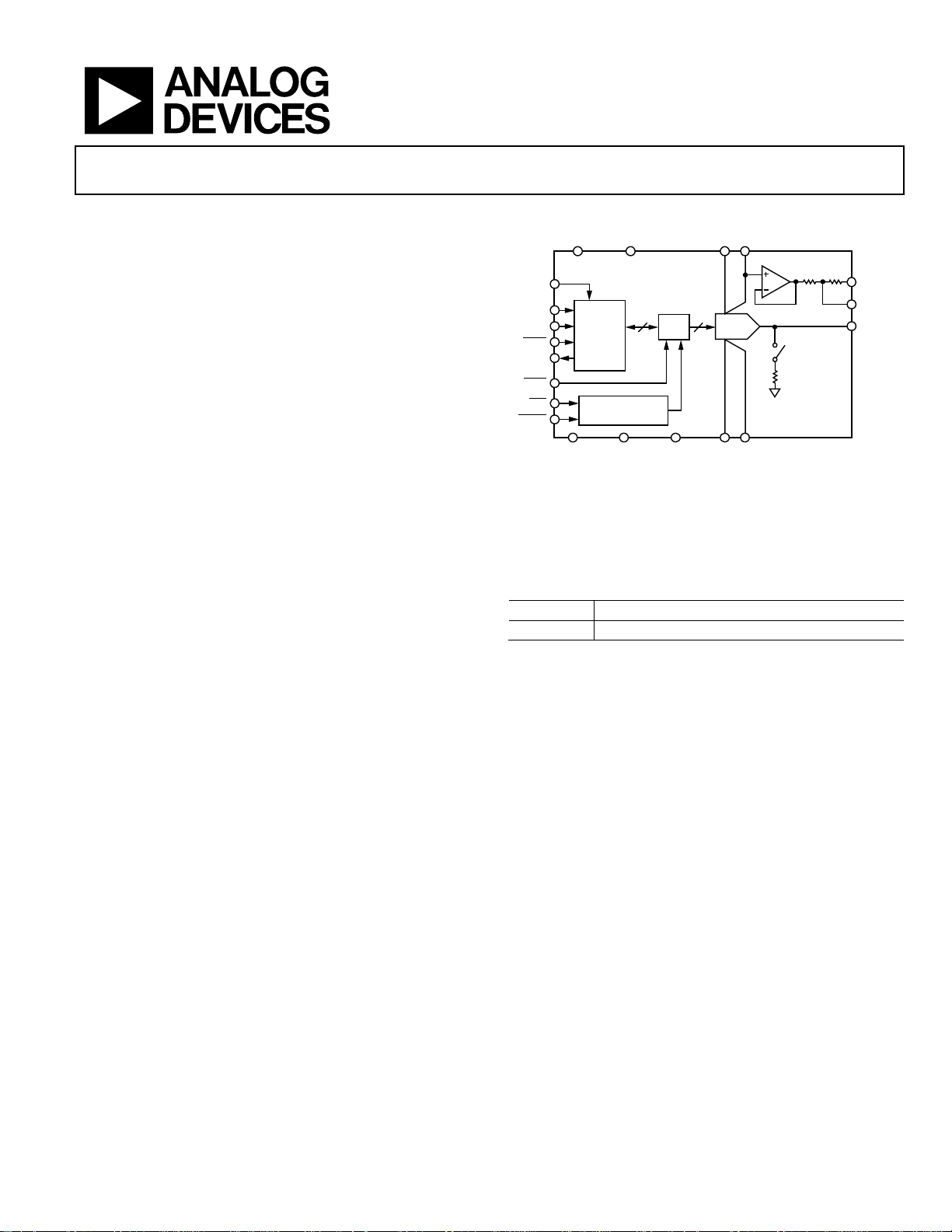
FUNCTIONAL BLOCK DIAGRAM
Figure 1.
COMPANION PRODUCTS
Ultra precision op amps: AD8675, AD8676
High voltage op amp: ADA4898-1
Additional companion products on the AD5791 product page
Table 1. Related Device
Part No. Description
AD5781 18-bit, 0.5 LSB INL, voltage output DAC
GENERAL DESCRIPTION
The AD5791-EP1 is a single 20-bit, unbuffered voltage-output
DAC that operates from a bipolar supply of up to 33 V. T he
AD5791 accepts a positive reference input in the range 5 V to
V
− 2.5 V and a negative reference input in the range VSS +
DD
2.5 V to 0 V. T h e AD5791-EP offers a relative accuracy
specification of ±1 LSB max, and operation is guaranteed
monotonic with a ±1 LSB DNL maximum specification.
The part uses a versatile 3-wire serial interface that operates at
clock rates up to 35 MHz and that is compatible with standard
SPI, QSPI™, MICROWIRE™, and DSP interface standards. The
part incorporates a power-on reset circuit that ensures the DAC
output powers up to 0 V in a known output impedance state
and remains in this state until a valid write to the device takes
1
Protected by U.S. Patents No. 7,884,747 and 8,089,380. Other patents pending.
Information furnished by Analog Devices is believed to be accurate and reliable. However, no
responsibility is assumed by Analog Devices for its use, nor for any infringements of patents or other
license is granted by implication or otherwise under any patent or patent rights of Analog Devices.
place. The part provides an output clamp feature that places the
output in a defined load state.
The AD5791-EP is available in a compact, 20-lead TSSOP
package and operates at the extended automotive temperature
range of −55°C to +125°C. Additional application and technical
information can be found in the AD5791 data sheet.
PRODUCT HIGHLIGHTS
1. 1 ppm Accuracy.
2. Wide Power Supply Range up to ±16.5 V.
3. Operating Temperature Range: −55°C to +125°C.
4. Low 7.5 nV/√Hz Noise Spectral Density.
5. Low 0.05 ppm/°C Temperature Drift.
One Technology Way, P.O. Box 9106, Norwood, MA 02062-9106, U.S.A.
Tel: 781.329.4700 www.analog.com
Page 2

AD5791-EP Enhanced Product
TABLE OF CONTENTS
Features .............................................................................................. 1
Enhanced Product Features ............................................................ 1
Applications ....................................................................................... 1
Functional Block Diagram .............................................................. 1
Companion Products ....................................................................... 1
General Description ......................................................................... 1
Product Highlights ........................................................................... 1
Revision History ............................................................................... 2
REVISION HISTORY
2/12—Revision 0: Initial Version
Specifications .....................................................................................3
Timing Characteristics .................................................................5
Absolute Maximum Ratings ............................................................8
ESD Caution...................................................................................8
Pin Configuration and Function Descriptions ..............................9
Typical Performance Characteristics ........................................... 10
Outline Dimensions ....................................................................... 18
Ordering Guide .......................................................................... 18
Rev. 0 | Page 2 of 20
Page 3

Enhanced Product AD5791-EP
Full-Scale Error
−7
±0.1
+7
LSB
±0.04
ppm FSR/°C
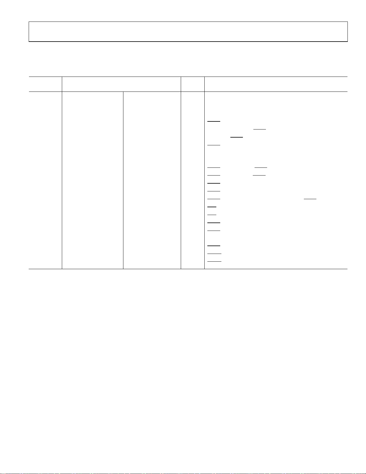
SPECIFICATIONS
VDD = 12.5 V to 16.5 V, VSS = −16.5 V to −12.5 V, V
R
= unloaded, CL = unloaded, all specifications T
L
Table 2.
Parameter1 Min Typ Max Unit Test Conditions/Comments
STATIC PERFORMANCE2
Resolution 20 Bits
Integral Nonlinearity Error (Relative Accuracy) −1 ±0.25 +1 LSB V
−1.5 ±0.25 +1.5 LSB V
−1.5 ±0.5 +1.5 LSB V
−3 ±1 +3 LSB
Differential Nonlinearity Error −1 ±0.5 +1 LSB V
−1.5 ±0.75 +1.5 LSB V
−2.5 ±1 +2.5 LSB V
Linearity Error Long-Term Stability4 0.16 LSB After 500 hours at TA = 125°C
0.19 LSB After 1000 hours at TA = 125°C
0.11 LSB After 1000 hours at TA = 100°C
−11 ±0.25 +11 LSB
−21 ±0.8 +21 LSB
−4 ±0.1 +4 LSB
−4 ±0.25 +4 LSB
−6 ±0.8 +6 LSB
Full-Scale Error Temperature Coefficient ±0.02 ppm FSR/°C
Zero-Scale Error −7 ±0.1 +7 LSB
−10 ±0.15 +10 LSB
−21 ±0.75 +21 LSB
−4 ±0.1 +4 LSB
−4 ±0.15 +4 LSB
−6 ±0.75 +6 LSB
Zero-Scale Error Temperature Coefficient3
Gain Error −6 ±0.3 +6 ppm FSR
−10 ±0.4 +10 ppm FSR
−20 ±0.4 +20 ppm FSR
−6 ±0.3 +6 ppm FSR
−6 ±0.4 +6 ppm FSR
−7 ±0.4 +7 ppm FSR
Gain Error Temperature Coefficient3
R1, RFB Matching 0.01 %
OUTPUT CHARACTERISTICS3
Output Voltage Range V
Output Slew Rate 50 V/µs
Output Voltage Settling Time 1 µs 10 V step to 0.02%, using the AD845 buffer
1 µs 500 code step to ±1 LSB5
Output Noise Spectral Density 7.5 nV/√Hz at 1 kHz, DAC code = midscale
7.5 nV/√Hz at 10 kHz, DAC code = midscale
7.5 nV/√Hz At 100 kHz, DAC code = midscale
Output Voltage Noise 1.1 µV p-p DAC code = midscale, 0.1 Hz to 10 Hz
MIN
REFP
to T
= 10 V, V
MAX
= −10 V, VCC = 2.7 V to +5.5 V, IOVCC = 1.71 V to 5.5 V,
REFN
, unless otherwise noted.
±0.04 ppm FSR/°C
V
REFN
V
REFP
= +10 V, V
REFP
= 0°C to 105°C
T
A
= +10 V, V
REFP
= 10 V, V
REFP
V
= 5 V, V
REFP
= +10 V, V
REFP
= 10 V, V
REFP
= 5 V, V
REFP
V
= +10 V, V
REFP
V
= 10 V, V
REFP
V
= 5 V, V
REFP
V
= +10 V, V
REFP
V
= 10 V, V
REFP
V
= 5 V, V
REFP
V
= +10 V, V
REFP
V
= 10 V, V
REFP
V
= 5 V, V
REFP
V
= +10 V, V
REFP
V
= 10 V, V
REFP
V
= 5 V, V
REFP
V
= +10 V, V
REFP
V
= 10 V, V
REFP
V
= 5 V, V
REFP
V
= +10 V, V
REFP
V
= 10 V, V
REFP
V
= 5 V, V
REFP
REFN
REFN
= 0 V3
REFN
= 0 V3
REFN
REFN
= 0 V
REFN
= 0 V
REFN
REFN
= 0 V3
REFN
= 0 V3
REFN
= −10 V3, TA = 0°C to 105°C
REFN
= 0 V3, TA = 0°C to 105°C
REFN
= 0 V3, TA = 0°C to 105°C
REFN
REFN
= 0 V3
REFN
= 0 V3
REFN
= −10 V3, TA = 0°C to 105°C
REFN
= 0 V3, TA = 0°C to 105°C
REFN
= 0 V3, TA = 0°C to 105°C
REFN
REFN
= 0 V3
REFN
= 0 V3
REFN
= −10 V3, TA = 0°C to 105°C
REFN
= 0 V3, TA = 0°C to 105°C
REFN
= 0 V3, TA = 0°C to 105°C
REFN
in unity-gain mode
6
bandwidth
= −10 V,
= −10 V
= −10 V
= −10 V3
= −10 V3
= −10 V3
Rev. 0 | Page 3 of 20
Page 4

AD5791-EP Enhanced Product
Spurious Free Dynamic Range
100 dB
1 kHz tone, 10 kHz sample rate
Output High Voltage, VOH
IOVCC − 0.5 V
V
IOVCC = 1.71 V to 5.5 V, sourcing 1 mA
High Impedance Leakage Current
±1
µA
95 dB
VDD ± 200 mV, 50 Hz/60 Hz, V
= −15 V
Parameter1 Min Typ Max Unit Test Conditions/Comments
Midscale Glitch Impulse7 3.1 nV-sec V
1.7 nV-sec V
1.4 nV-sec V
MSB Segment Glitch Impulse7
9.1 nV-sec V
3.6 nV-sec V
1.9 nV-sec V
Output Enabled Glitch Impulse 45 nV-sec On removal of output ground clamp
Digital Feedthrough 0.4 nV-sec
DC Output Impedance (Normal Mode) 3.4 kΩ
DC Output Impedance (Output Clamped
6 kΩ
to Ground)
Total Harmonic Distortion 97 dB 1 kHz tone, 10 kHz sample rate
REFERENCE INPUTS3
V
Input Range 5 VDD − 2.5 V V
REFP
V
Input Range VSS + 2.5 V 0
REFN
DC Input Impedance 5 6.6 kΩ V
Input Capacitance 15 pF V
LOGIC INPUTS3
Input Current8 −1 +1 µA
Input Low Voltage, VIL 0.3 × IOVCC V IOVCC = 1.71 V to 5.5 V
Input High Voltage, VIH 0.7 × IOVCC V IOVCC = 1.71 V to 5.5 V
Pin Capacitance 5 pF
LOGIC OUTPUT (SDO)3
Output Low Voltage, VOL 0.4 V IOVCC = 1.71 V to 5.5 V, sinking 1 mA
= +10 V, V
REFP
= 10 V, V
REFP
= 5 V, V
REFP
= +10 V, V
REFP
= 10 V, V
REFP
= 5 V, V
REFP
, V
REFP
REFN
= −10 V
REFN
= 0 V
REFN
= 0 V
REFN
= −10 V, see Figure 43
REFN
= 0 V, see Figure 44
REFN
= 0 V, see Figure 45
REFN
, code dependent,
typical at midscale code
, V
REFP
REFN
High Impedance Output Capacitance 3 pF
POWER REQUIREMENTS All digital inputs at DGND or IOVCC
VDD 7.5 VSS + 33 V
VSS VDD − 33 −2.5 V
VCC 2.7 5.5 V
IOVCC 1.71 5.5 V IOVCC ≤ VCC
IDD 4.2 5.2 mA
ISS 4 4.9 mA
ICC 600 900 µA
IOICC 52 140 µA SDO disabled
DC Power Supply Rejection Ratio
3, 9
±0.6 µV/V V
± 10%, V
DD
= 15 V
SS
±0.6 µV/V VSS ± 10%, VDD = 15 V
AC Power Supply Rejection Ratio3
SS
95 dB ∆VSS ± 200 mV, 50 Hz/60 Hz, VDD = 15 V
1
Temperature range: −55°C to +125°C, typical at +25°C and VDD = +15 V, VSS = −15 V, V
2
Performance characterized with AD8676BRZ voltage reference buffers and AD8675ARZ output buffer.
3
Guaranteed by design and characterization; not production tested.
4
Linearity error refers to both INL error and DNL error, either parameter can be expected to drift by the amount specified after the length of time specified.
5
AD5791-EP configured in ×2 gain mode, 25 pF compensation capacitor on AD797.
6
Includes noise contribution from AD8676BRZ voltage reference buffers.
7
The AD5791-EP is configured in bias compensation mode with a low-pass RC filter on the output. R = 300 Ω, C = 143 pF (total capacitance seen by the output buffer,
lead capacitance, and so forth).
8
Current flowing in an individual logic pin.
9
Includes PSRR of AD8676BRZ voltage reference buffers.
= +10 V, V
REFP
= −10 V.
REFN
Rev. 0 | Page 4 of 20
Page 5
Enhanced Product AD5791-EP
t3 9 5
ns min
SCLK low time
t9
12 7 ns min
Data hold time
t20 0 0
ns min
SYNC rising edge to SCLK rising edge ignore
TIMING CHARACTERISTICS
VCC = 2.7 V to 5.5 V; all specifications T
MIN
to T
, unless otherwise noted.
MAX
Table 3.
1
Limit
Parameter
2
t
40 28 ns min SCLK cycle time
1
IOVCC = 1.71 V to 3.3 V IOVCC = 3.3 V to 5.5 V
Unit Test Conditions/Comments
92 60 ns min SCLK cycle time (readback and daisy-chain modes)
t2 15 10 ns min SCLK high time
t4 5 5 ns min
t5 2 2 ns min
t6 48 40 ns min
t7 8 6 ns min
SYNC to SCLK falling edge setup time
SCLK falling edge to
Minimum
SYNC high time
SYNC rising edge hold time
SYNC rising edge to next SCLK falling edge ignore
t8 9 7 ns min Data setup time
t10 13 10 ns min
t11 20 16 ns min
t12 14 11 ns min
t13 130 130 ns typ
t14 130 130 ns typ
t15 50 50 ns min
t16 140 140 ns typ
t17 0 0 ns min
t18 65 60 ns max
LDAC falling edge to SYNC falling edge
SYNC rising edge to LDAC falling edge
LDAC pulse width low
LDAC falling edge to output response time
SYNC rising edge to output response time (LDAC tied low)
CLR pulse width low
CLR pulse activation time
SYNC falling edge to first SCLK rising edge
SYNC rising edge to SDO tristate (CL = 50 pF)
t19 62 45 ns max SCLK rising edge to SDO valid (CL = 50 pF)
t21 35 35 ns typ
t22 150 150 ns typ
1
All input signals are specified with tR = tF = 1 ns/V (10% to 90% of IOVCC) and timed from a voltage level of (VIL + VIH)/2.
2
Maximum SCLK frequency is 35 MHz for write mode and 16 MHz for readback and daisy-chain modes.
RESET pulse width low
RESET pulse activation time
Rev. 0 | Page 5 of 20
Page 6
AD5791-EP Enhanced Product
t
7
2421
DB23 DB0
t
10
t
8
t
4
t
6
t
5
t
3
t
1
t
2
t
9
t
11
t
12
t
13
t
14
t
15
t
16
t
21
t
22
V
OUT
V
OUT
V
OUT
V
OUT
RESET
CLR
LDAC
SDIN
SYNC
SCLK
10455-002
DB23 DB0
NOP CONDITION
REGISTER CONTENTS CLOCKED OUT
t
1
t
17
t
2
t
5
t
17
t
5
t
19
t
18
t
20
t
3
t
4
t
8
t
9
t
6
t
7
24221 24 1
DB23 DB0
INPUT WORD SPECIFIES
REGISTER TO BE READ
SDO
SDIN
SYNC
SCLK
10455-003
Figure 2. Write Mode Timing Diagram
Figure 3. Readback Mode Timing Diagram
Rev. 0 | Page 6 of 20
Page 7

Enhanced Product AD5791-EP
1 2 24
48
25
26
INPUT WORD FOR DAC N
INPUT WORD FOR DAC N – 1
INPUT WORD FOR DAC N
UNDEFINED
t
20
t
1
t
2
t
19
t
3
t
17
t
4
t
9
t
8
t
6
t
18
t
5
DB23
DB23
DB0 DB23 DB0
DB0 DB23 DB0
SDO
SDIN
SYNC
SCLK
10455-004
Figure 4. Daisy-Chain Mode Timing Diagram
Rev. 0 | Page 7 of 20
Page 8

AD5791-EP Enhanced Product
VDD to AGND
−0.3 V to +34 V
V
to AGND
VSS − 0.3 V to + 0.3 V
ABSOLUTE MAXIMUM RATINGS
TA = 25°C, unless otherwise noted. Transient currents of up to
100 mA do not cause SCR latch-up.
Table 4.
Parameter Rating
VSS to AGND −34 V to +0.3 V
VDD to VSS −0.3 V to +34 V
VCC to DGND −0.3 V to +7 V
IOVCC to DGND
−0.3 V to V
+ 0.3 V or +7 V
CC
(whichever is less)
Digital Inputs to DGND
−0.3 V to IOV
+ 0.3 V or
CC
+7 V (whichever is less)
V
to AGND −0.3 V to VDD + 0.3 V
OUT
V
to AGND −0.3 V to VDD + 0.3 V
REFPF
V
to AGND −0.3 V to VDD + 0.3 V
REFPS
REFNF
V
to AGND VSS − 0.3 V to + 0.3 V
REFNS
DGND to AGND −0.3 V to +0.3 V
Operating Temperature Range, TA
Industrial −55°C to + 125°C
Storage Temperature Range −65°C to +150°C
Maximum Junction Temperature,
max
T
J
150°C
Power Dissipation (TJ max − TA)/θJA
TSSOP Package
θJA Thermal Impedance 143°C/W
θJC Thermal Impedance 45°C/W
Lead Temperature JEDEC industry standard
Soldering J-STD-020
ESD (Human Body Model) 1.5 kV
Stresses above those listed under Absolute Maximum Ratings
may cause permanent damage to the device. This is a stress
rating only; functional operation of the device at these or any
other conditions above those indicated in the operational
section of this specification is not implied. Exposure to absolute
maximum rating conditions for extended periods may affect
device reliability.
This device is a high performance integrated circuit with an
ESD rating of 1.5 kV, and it is ESD sensitive. Proper precautions
should be taken for handling and assembly.
ESD CAUTION
Rev. 0 | Page 8 of 20
Page 9
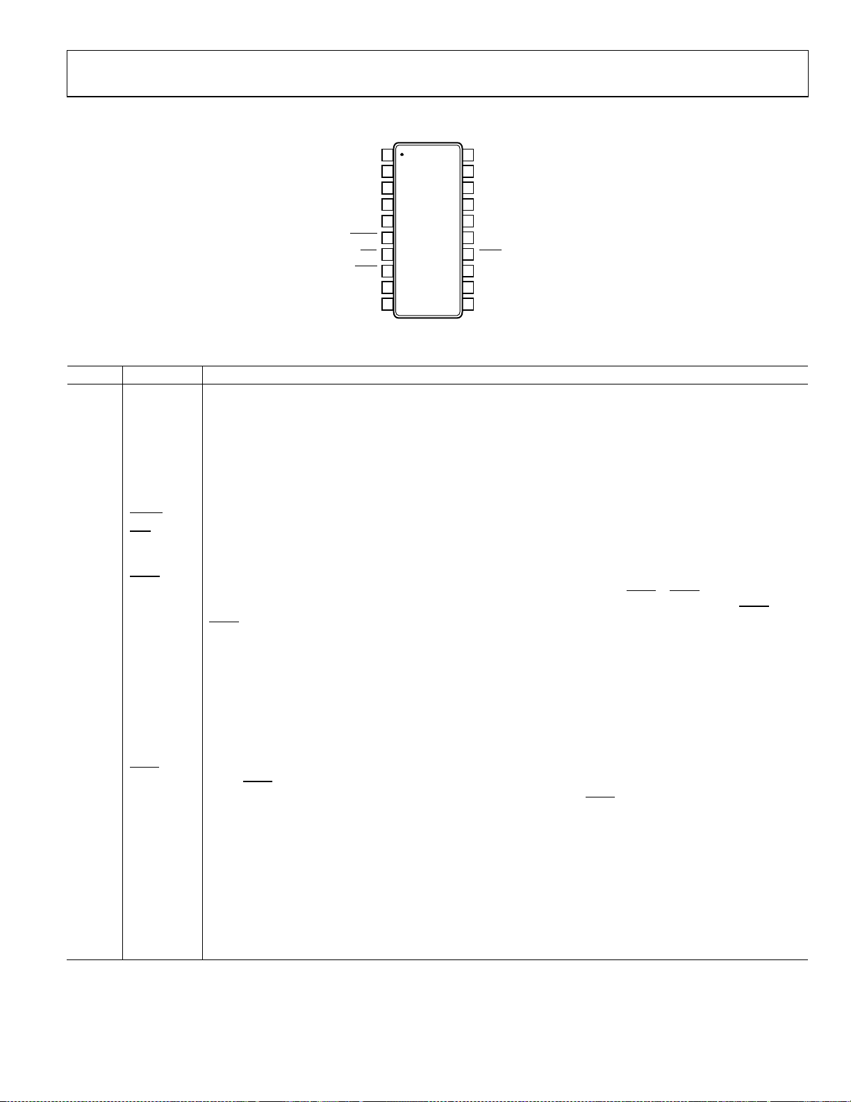
Enhanced Product AD5791-EP
1
2
3
4
5
6
7
8
9
10
V
OUT
V
REFPS
V
REFPF
CLR
RESET
V
DD
INV
IOV
CC
V
CC
LDAC
20
19
18
17
16
15
14
13
12
11
AGND
V
SS
V
REFNS
SYNC
DGND
V
REFNF
SDO
SDIN
SCLK
R
FB
AD5791-EP
TOP VIEW
(Not to S cale)
10455-005
PIN CONFIGURATION AND FUNCTION DESCRIPTIONS
Figure 5. Pin Configuration
Table 5. Pin Function Descriptions
Pin No. Mnemonic Description
1 INV Connection to Inverting Input of External Amplifier.
2 V
3 V
4 V
5 VDD
Analog Output Voltage.
OUT
REFPS
Positive Reference Sense Voltage Input. A voltage range of 5 V to V
amplifier must be connected at this pin in conjunction with the V
REFPF
Positive Reference Force Voltage Input. A voltage range of 5 V to V
amplifier must be connected at this pin in conjunction with the V
Positive Analog Supply Connection. A voltage range of 7.5 V to 16.5 V can be connected; V
− 2.5 V can be connected. A unity gain
DD
pin.
REFPF
− 2.5 V can be connected. A unity gain
DD
pin.
REFPS
should be decoupled
DD
to AGND.
6
7
RESET
CLR Active Low Clear Logic Input Pin. Asserting this pin sets the DAC register to a user defined value and updates the
Active Low Reset Logic Input Pin. Asserting this pin returns the AD5791-EP to its power-on status.
DAC output. The output value depends on the DAC register coding that is being used, either binary or twos
complement.
8
LDAC Active Low Load DAC Logic Input Pin. This is used to update the DAC register and, consequently, the analog
output. When tied permanently low, the output is updated on the rising edge of
SYNC. If LDAC is held high during
the write cycle, the input register is updated, but the output update is held off until the falling edge of
LDAC pin should not be left unconnected.
9 VCC Digital Supply Connection. A voltage range of 2.7 V to 5.5 V can be connected. VCC should be decoupled to DGND.
10 IOVCC
Digital Interface Supply Pin. Digital threshold levels are referenced to the voltage applied to this pin. A voltage in
the range of 1.71 V to 5.5 V can be connected. IOV
should not be allowed to exceed VCC.
CC
11 SDO Serial Data Output Pin. Data is clocked out on the rising edge of the serial clock input.
12 SDIN
Serial Data Input Pin. This device has a 24-bit shift register. Data is clocked into the register on the falling edge of
the serial clock input.
13 SCLK
Serial Clock Input. Data is clocked into the input shift register on the falling edge of the serial clock input. Data can
be transferred at clock rates of up to 35 MHz.
14
SYNC Active Low Digital Interface Synchronization Input Pin. This is the frame synchronization signal for the input data.
When
SYNC is low, it enables the input shift register, and data is then transferred in on the falling edges of the
following clocks. The input shift register is updated on the rising edge of SYNC.
15 DGND Ground Reference Pin for Digital Circuitry.
16 V
17 V
18 VSS
REFNF
REFNS
Negative Reference Force Voltage Input. A voltage range of V
amplifier must be connected at this pin in conjunction with the V
Negative Reference Sense Voltage Input. A voltage range of V
amplifier must be connected at this pin in conjunction with the V
Negative Analog Supply Connection. A voltage range of −16.5 V to −2.5 V can be connected. V
+ 2.5 V to 0 V can be connected. A unity gain
SS
pin.
REFNS
+ 2.5 V to 0 V can be connected. A unity gain
SS
pin.
REFNF
should be
SS
decoupled to AGND.
19 AGND Ground Reference Pin for Analog Circuitry.
20 RFB Feedback Connection for External Amplifier.
Rev. 0 | Page 9 of 20
LDAC. The
Page 10

AD5791-EP Enhanced Product
1.0
0.8
0.6
0.4
0.2
0
–0.2
–0.4
–0.6
–0.8
–1.0
0 200000 400000 600000 800000 1000000
DAC CODE
INL ERROR ( LSB)
T
A
= +125°C
T
A
= +25°C
T
A
= –40°C
AD8676 REFERENCE BUF FERS
AD8675 OUTPUT BUFFER
V
REFP
= +10V
V
REFN
= –10V
V
DD
= +15V
V
SS
= –15V
10455-006
1.5
1.0
0.5
0
–0.5
–1.0
–1.5
0 200000 400000 600000 800000 1000000
DAC CODE
INL ERROR ( LSB)
T
A
= +125°C
T
A
= +25°C
T
A
= –40°C
AD8676 REFERENCE BUF FERS
AD8675 OUTPUT BUFFER
V
REFP
= +10V
V
REFN
= 0V
V
DD
= +15V
V
SS
= –15V
10455-007
2.5
2.0
1.5
1.0
0.5
0
–0.5
–1.0
–1.5
–2.0
–2.5
0 200000 400000 600000 800000 1000000
DAC CODE
INL ERROR ( LSB)
TA = +125°C
T
A
= +25°C
T
A
= –40°C
AD8676 REFERENCE BUF FERS
AD8675 OUTPUT BUFFER
V
REFP
= +5V
V
REFN
= 0V
V
DD
= +15V
V
SS
= –15V
10455-008
0.8
0.6
0.4
0.2
0
–0.2
–0.4
–0.6
–0.8
0 200000 400000 600000 800000 1000000
DAC CODE
INL ERROR ( LSB)
AD8676 REFERENCE BUF FERS
AD8675 OUTPUT BUFFER
T
A
= –40°C
T
A
= +125°C
T
A
= +25°C
V
REFP
= +10V
V
REFN
= 0V
V
DD
= +15V
V
SS
= –15V
10455-009
1.0
0.8
0.6
0.4
0.2
0
–0.2
–0.4
–0.6
–0.8
–1.0
0 200000 400000 600000 800000 1000000
DAC CODE
DNL ERROR (L S B)
T
A
= +125°C
T
A
= +25°C
T
A
= –40°C
AD8676 REFERENCE BUF FERS
AD8675 OUTPUT BUFFER
V
REFP
= +10V
V
REFN
= –10V
V
DD
= +15V
V
SS
= –15V
10455-010
1.5
1.0
0.5
0
–0.5
–1.0
–1.5
0 200000 400000 600000 800000 1000000
DAC CODE
DNL ERROR (L S B)
TA = +125°C
T
A
= +25°C
T
A
= –40°C
V
REFP
= +10V
V
REFN
= 0V
V
DD
= +15V
VSS = –15V
AD8676 REFERENCE BUF FERS
AD8675 OUTPUT BUFFER
10455-011
TYPICAL PERFORMANCE CHARACTERISTICS
Figure 6. Integral Nonlinearity Error vs. DAC Code, ±10 V Span
Figure 7. Integral Nonlinearity Error vs. DAC Code, 10 V Span
Figure 9. Integral Nonlinearity Error vs. DAC Code, ±10 V Span, ×2 Gain Mode
Figure 10. Differential Nonlinearity Error vs. DAC Code, ±10 V Span
Figure 8. Integral Nonlinearity Error vs. DAC Code, 5 V Span
Figure 11. Differential Nonlinearity Error vs. DAC Code, 10 V Span
Rev. 0 | Page 10 of 20
Page 11

Enhanced Product AD5791-EP
2.0
1.5
1.0
0.5
0
–0.5
–1.0
–1.5
–2.0
0 200000 400000 600000 800000 1000000
DAC CODE
DNL ERROR (L S B)
V
REFP
= +5V
V
REFN
= 0V
V
DD
= +15V
V
SS
= –15V
T
A
= +125°C
T
A
= +25°C
T
A
= –40°C
AD8676 REFERENCE BUF FERS
AD8675 OUTPUT BUFFER
10455-012
1.0
0.8
0.6
0.4
0.2
0
–0.2
–0.4
–0.6
–0.8
–1.0
0 200000 400000 600000 800000 1000000
DAC CODE
DNL ERROR (L S B)
AD8676 REFERENCE BUF FERS
AD8675 OUTPUT BUFFER
V
REFP
= +10V
V
REFN
= 0V
V
DD
= +15V
V
SS
= –15V
T
A
= +25°C
T
A
= –40°C
T
A
= +125°C
10455-013
1.0
1.5
2.0
0.5
0
–0.5
–1.0
–1.5
–55 –35 –15 5 25 45 65 85 105 125
TEMPERATURE (°C)
INL ERROR ( LSB)
±10V SPAN MAX INL
+5V SPAN MAX INL
+10V SPAN MIN INL
+10V SPAN MAX INL
±10V SPAN MIN INL
+5V SPAN MIN INL
AD8676 REFERENCE BUF FERS
AD8675 OUTPUT BUFFER
V
DD
= +15V
V
SS
= –15V
10455-014
1.0
0.5
0
–0.5
–1.0
–1.5
–55 –35 –15 5 25 45 65 85 105 125
TEMPERATURE (°C)
DNL ERROR (L S B)
±10V SPAN MAX DNL
+5V SPAN MAX DNL
+10V SPAN MIN DNL
+10V SPAN MAX DNL
±10V SPAN MIN DNL
+5V SPAN MIN DNL
AD8676 REFERENCE BUF FERS
AD8675 OUTPUT BUFFER
V
DD
= +15V
V
SS
= –15V
10455-015
0.6
0.5
0.4
0.3
0.2
0.1
0
–0.2
–0.1
–0.3
12.
5 13.0 13.5 14.0 14.5 15.0 15.5 16.0 16.5
V
DD
/|VSS| (V)
INL ERROR ( LSB)
TA = 25°C
V
REFP
= +10V
V
REFN
= –10V
AD8676 REFERENCE BUF FERS
AD8675 OUTPUT BUFFER
INL MAX
INL MIN
10455-016
1.5
1.0
0.5
0
–0.5
–1.0
–1.5
7.5 8.5 9.5 10.5 11.5 12.5 13.5 14.5 15.5 16.5
V
DD
(V)
INL ERROR ( LSB)
–2.5 –3.9 –5.3 –6.7 –9.1 –10.5 –12.9 –14.2 –15.5 –16.5
V
SS
(V)
TA = 25°C
V
REFP
= +5V
V
REFN
= 0V
AD8676 REFERENCE BUF FERS
AD8675 OUTPUT BUFFER
INL MAX
INL MIN
10455-017
Figure 12. Differential Nonlinearity Error vs. DAC Code, 5 V Span
Figure 13. Differential Nonlinearity Error vs. DAC Code, ±10 V Span,
×2 Gain Mode
Figure 15. Differential Nonlinearity Error vs. Temperature
Figure 16. Integral Nonlinearity Error vs. Supply Voltage, ±10 V Span
Figure 14. Integral Nonlinearity Error vs. Temperature
Figure 17. Integral Nonlinearity Error vs. Supply Voltage, 5 V Span
Rev. 0 | Page 11 of 20
Page 12

AD5791-EP Enhanced Product
0.4
0.3
0.2
0.1
0
–0.1
–0.2
–0.3
–0.4
12.5 13.0 13.5 14.
0 14.5 15.0 15.5 16.0 16.5
V
DD
/|VSS| (V)
DNL ERROR (L S B)
T
A
= 25°C
V
REFP
= +10V
V
REFN
= –10V
AD8676 REFERENCE BUF FERS
AD8675 OUTPUT BUFFER
DNL MAX
DNL MIN
10455-018
0.4
0.2
0
–0.6
–0.4
–0.2
–0.8
–1.0
7.5 8.5 9.5 10.5 11.5 12.5 13.5
14.5 15.
5 16.5
V
DD
(V)
DNL ERROR (L S B)
–2.5 –3.9 –5.3 –6.7 –9.1 –10.5 –12.9 –14.2 –15.5 –16.5
V
SS
(V)
TA = 25°C
V
REFP
= +5V
V
REFN
= 0V
AD8676 REFERENCE BUF FERS
AD8675 OUTPUT BUFFER
DNL MAX
DNL MIN
10455-019
0.6
0.5
0.4
0.3
0.2
0.1
0
12.5 13.0 13.5 14.0 14.5 15.0 15.5 16.
0 16.5
V
DD
/|VSS| (V)
ZERO-SCALE ERROR (LS B)
TA = 25°C
V
REFP
= +10V
V
REFN
= –10V
AD8676 REFERENCE BUF FERS
AD8675 OUTPUT BUFFER
10455-020
0.6
0.5
0.4
0.1
0.2
0.3
0
7.5 8.5 9.5 10.5 11.5 12.5 13.5 14.5 15.5 16.5
V
DD
(V)
ZERO-SCALE ERROR (LS B)
–2.5 –3.9 –5.3 –6.7 –9.1 –10.5 –12.9 –14.2 –15.5 –16.5
V
SS
(V)
TA = 25°C
V
REFP
= +5V
V
REFN
= 0V
AD8676 REFERENCE BUF FERS
AD8675 OUTPUT BUFFER
10455-021
0.20
0.15
0.10
0.05
0
–0.05
–0.10
–0.15
12.5 13.0 13.5 14.0 14.5 15.0 15.5 16.0 16.5
V
DD
/|VSS| (V)
MIDSCALE E RROR (LSB)
TA = 25°C
V
REFP
= +10V
V
REFN
= –10V
AD8676 REFERENCE BUF FERS
AD8675 OUTPUT BUFFER
10455-022
0.2
0.1
0
–0.5
–0.6
–0.3
–0.4
–0.1
–0.2
–0.7
7.5 8.5 9.5 10.5 11.5 12.5 13.5 14.5 15.5 16.5
V
DD
(V)
MIDSCALE E RROR (LSB)
–2.5 –3.9 –5.3 –6.7 –9.1 –10.5 –12.9 –14.2 –15.5 –16.5
V
SS
(V)
T
A
= 25°C
V
REFP
= +5V
V
REFN
= 0V
AD8676 REFERENCE BUF FERS
AD8675 OUTPUT BUFFER
10455-023
Figure 18. Differential Nonlinearity Error vs. Supply Voltage, ±10 V Span
Figure 19. Differential Nonlinearity Error vs. Supply Voltage, 5 V Span
Figure 21. Zero-Scale Error vs. Supply Voltage, 5 V Span
Figure 22. Midscale Error vs. Supply Voltage, ±10 V Span
Figure 20. Zero-Scale Error vs. Supply Voltage, ±10 V Span
Figure 23. Midscale Error vs. Supply Voltage, 5 V Span
Rev. 0 | Page 12 of 20
Page 13

Enhanced Product AD5791-EP
–0.015
–0.035
–0.055
–0.075
–0.095
–0.115
–0.135
–0.155
–0.175
–0.195
12.5 13.0 13.5 14.0 14.5 15.0 15.5 16.0 16.5
V
DD
/|V
SS
| (V)
FULL-S CALE ERROR (LSB)
T
A
= 25°C
V
REFP
= +10V
V
REFN
= –10V
AD8676 REFERENCE BUF FERS
AD8675 OUTPUT BUFFER
10455-024
0.25
0.20
0.15
0.10
0.05
0
–0.05
7.5 8.5 9.5 10.5 11.5 12.5 13.5 14.5 15.5 16.5
V
DD
(V)
FULL-S CALE ERROR (LS B)
–2.5 –3.9 –5.3 –6.7 –9.1 –10.5 –12.9 –14.2 –15.5 –16.5
V
SS
(V)
T
A
= 25°C
V
REFP
= +5V
V
REFN
= 0V
AD8676 REFERENCE BUF FERS
AD8675 OUTPUT BUFFER
10455-025
–0.30
–0.35
–0.40
–0.45
–0.50
–0.55
–0.60
–0.65
12.5 13.0 13.5 14.0 14.5 15.0 15.5 16.0 16.5
V
DD
/|VSS| (V)
GAIN ERROR ( ppm FSR)
TA = 25°C
V
REFP
= +10V
V
REFN
= –10V
AD8676 REFERENCE BUF FERS
AD8675 OUTPUT BUFFER
10455-026
0.10
0.05
0
–0.35
–0.30
–0.25
–0.20
–0.15
–0.10
–0.05
–0.40
7.5 8.5 9.5 10.5 11.5 12.5 13.5 14.5 15.5 16.5
V
DD
(V)
GAIN ERROR ( ppm FSR)
–2.5 –3.9 –5.3 –6.7 –9.1 –10.5 –12.9 –14.2 –15.5 –16.5
V
SS
(V)
T
A
= 25°C
V
REFP
= +5V
V
REFN
= 0V
AD8676 REFERENCE BUF FERS
AD8675 OUTPUT BUFFER
10455-027
0.6
0.4
0.2
0
–0.2
–0.4
–0.6
5.0 5.5 6.0 6.5 7.0 7.5 8.0 8.5 9.0 9.5 10.0
V
REFP
/|V
REFN
| (V)
INL ERROR ( LSB)
T
A
= 25°C
V
DD
= +15V
V
SS
= –15V
AD8676 REFERENCE BUF FERS
AD8675 OUTPUT BUFFER
INL MAX
INL MIN
10455-028
0.4
0.2
0.3
0.1
0
–0.1
–0.2
–0.3
–0.5
–0.4
–0.6
5.0 5.5 6.0 6.5 7.0 7.5 8.0 8.5 9.0 9.5 10.0
V
REFP
/|V
REFN
| (V)
DNL ERROR (L S B)
DNL MAX
DNL MIN
TA = 25°C
V
DD
= +15V
V
SS
= –15V
AD8676 REFERENCE BUF FERS
AD8675 OUTPUT BUFFER
10455-029
Figure 24. Full-Scale Error vs. Supply Voltage, ±10 V Span
Figure 27. Gain Error vs. Supply Voltage, 5 V Span
Figure 25. Full-Scale Error vs. Supply Voltage, 5 V Span
Figure 26. Gain Error vs. Supply Voltage, ±10 V Span
Figure 28. Integral Nonlinearity Error vs. Reference Voltage
Figure 29. Differential Nonlinearity Error vs. Reference Voltage
Rev. 0 | Page 13 of 20
Page 14

AD5791-EP Enhanced Product
0.60
0.55
0.50
0.45
0.40
0.35
0.30
5.0 5.5 6.0 6.5 7.0 7.5 8.0 8.5 9.0 9.5 10.0
V
REFP
/|V
REFN
| (V)
ZERO-SCALE ERROR (LS B)
T
A
= 25°C
V
DD
= +15V
V
SS
= –15V
AD8676 REFERENCE BUF FERS
AD8675 OUTPUT BUFFER
10455-030
0.15
0.10
0.05
0
–0.05
–0.10
–0.15
–0.20
5.0 5.5 6.0 6.5 7.0 7.5 8.0 8.5 9.0 9.5 10.0
V
REFP
/|V
REFN
| (V)
MIDSCALE E RROR (LSB)
T
A
= 25°C
V
DD
= +15V
V
SS
= –15V
AD8676 REFERENCE BUF FERS
AD8675 OUTPUT BUFFER
10455-031
0.15
0.10
0.05
0
–0.05
–0.10
–0.15
–0.20
5.0 5.5 6.0 6.5 7.0 7.5 8.0 8.5 9.0
9.5 10.
0
V
REFP
/|V
REFN
| (V)
FULL-S CALE ERROR (LS B)
T
A
= 25°C
V
DD
= +15V
V
SS
= –15V
AD8676 REFERENCE BUF FERS
AD8675 OUTPUT BUFFER
10455-032
–0.30
–0.35
–0.40
–0.45
–0.50
–0.55
–0.60
5.0 5.5 6.0 6.5 7.0 7.5 8.0 8.5 9.0 9.5 10.0
V
REFP
/|V
REFN
| (V)
GAIN ERROR ( ppm FSR)
T
A
= 25°C
V
DD
= +15V
V
SS
= –15V
AD8676 REFERENCE BUF FERS
AD8675 OUTPUT BUFFER
10455-033
2.0
1.5
1.0
0.5
0
–0.5
–1.0
–1.5
–2.0
–2.5
–3.0
–55 –35 –15 5 25 45 65 85 105 125
TEMPERATURE (°C)
FULL-S CALE ERROR (LS Bs)
±10V SPAN
+10V SPAN
+5V SPAN
AD8676 REFERENCE BUF FERS
AD8675 OUTPUT BUFFER
V
DD
= +15V
V
SS
= –15V
10455-034
2.0
1.8
1.6
1.4
1.2
1
0.8
0.6
0.4
0.2
0
–55 –35 –15 5 25 45 65 85 105 125
TEMPERATURE (°C)
MIDSCALE E RROR (LSBs)
±10V SPAN
+10V SPAN
+5V SPAN
AD8676 REFERENCE BUF FERS
AD8675 OUTPUT BUFFER
V
DD
= +15V
V
SS
= –15V
10455-035
Figure 30. Zero-Scale Error vs. Reference Voltage
Figure 31. Midscale Error vs. Reference Voltage
Figure 33. Gain Error vs. Reference Voltage
Figure 34. Full-Scale Error vs. Temperature
Figure 32. Full-Scale Error vs. Reference Voltage
Figure 35. Midscale Error vs. Temperature
Rev. 0 | Page 14 of 20
Page 15

Enhanced Product AD5791-EP
5
4
3
2
1
0
–1
–2
–3
–4
–5
–55 –35 –15 5 25 45 65 85 105 125
TEMPERATURE (°C)
ZERO-SCALE ERROR (LS Bs)
±10V SPAN
+10V SPAN
+5V SPAN
AD8676 REFERENCE BUF FERS
AD8675 OUTPUT BUFFER
V
DD
= +15V
V
SS
= –15V
10455-036
4
3
2
1
0
–1
–2
–3
–4
–5
–55 –35 –15 5 25 45 65 85 105 125
TEMPERATURE (°C)
GAIN ERROR ( ppm FSR)
±10V SPAN
+10V SPAN
+5V SPAN
AD8676 REFERENCE BUF FERS
AD8675 OUTPUT BUFFER
V
DD
= +15V
V
SS
= –15V
10455-037
900
800
700
600
500
400
300
200
100
0
0 1
T
A
= 25°C
2 3 4 5 6
LOGIC INPUT VOLTAGE (V)
IOI
CC
(µA)
IOVCC = 5V, LOGIC VOLTAGE
INCREASING
IOV
CC
= 5V, LOGIC VOLTAGE
DECREASING
IOV
CC
= 3V, LOGIC VOLTAGE
INCREASING
IOV
CC
= 3V, LOGIC VOLTAGE
DECREASING
10455-038
5
4
3
2
1
0
–1
–2
–3
–4
–5
–20 –15 –10 –5 0 5 10 15 20
V
DD/VSS
(V)
I
DD
, I
SS
(mA)
T
A
= 25°C
I
DD
I
SS
10455-039
CH3 5V CH4 5V 200ns
3
4
VDD = +15V
V
SS
= –15V
V
REFP
= +10V
V
REFN
= –10V
AD8676 REFERENCE BUF FERS
OUTPUT UNBUFFERED
LOAD = 10MΩ||20pF
10455-040
CH3 5V CH4 5V 200ns
3
4
VDD = +15V
V
SS
= –15V
V
REFP
= +10V
V
REFN
= –10V
AD8676 REFERENCE BUF FERS
OUTPUT UNBUFFERED
L
OAD = 10MΩ|| 20pF
10455-041
Figure 36. Zero-Scale Error vs. Temperature
Figure 37. Gain Error vs. Temperature
Figure 39. Power Supply Currents vs. Power Supply Voltages
Figure 40. Rising Full-Scale Voltage Step
Figure 38. IOICC vs. Logic Input Voltage
Figure 41. Falling Full-Scale Voltage Step
Rev. 0 | Page 15 of 20
Page 16

AD5791-EP Enhanced Product
10.8
10.6
10.4
10.2
10.0
9.8
9.6
9.4
0 1 5432
V
OUT
(mV)
TIME (µs)
±10V V
REF
OUTPUT GAIN OF 1
BIAS COMPE NSATION MODE
20pF COMP E NS ATION CAPACITOR
RC LOW-PASS FILTER
10455-042
10
0
1
2
3
4
5
6
7
8
9
16384
65536
OUTPUT GLITCH (nV–sec)
CODE
114688
163840
212992
262144
311296
360448
409600
458752
507904
557056
606208
655360
704512
753664
802816
851968
901120
950272
999424
POSITIVE CODE
CHANGE
NEGATIV E CODE
CHANGE
5V V
OUTPUT GAIN OF 1
BIAS COMPE NSATION MODE
20pF COMP E NS ATION CAPACITOR
RC LOW-PASS FILTER
REF
10455-043
4.0
0
2.0
1.5
1.0
0.5
2.5
3.0
3.5
16384
65536
OUTPUT GLITCH (nV–sec)
CODE
114688
163840
212992
262144
311296
360448
409600
458752
507904
557056
606208
655360
704512
753664
802816
851968
901120
950272
999424
POSITIVE CODE
CHANGE
NEGATIV E CODE
CHANGE
10V V
REF
OUTPUT GAIN OF 1
BIAS COMPE NSATION MODE
20pF COMP E NS ATION CAPACITOR
RC LOW-PASS FILTER
10455-044
3.0
–0.2
2.2
1.0
1.4
1.8
0.6
0.2
2.6
16384
65536
OUTPUT GLITCH (nV–sec)
CODE
114688
163840
212992
262144
311296
360448
409600
458752
507904
557056
606208
655360
704512
753664
802816
851968
901120
950272
999424
NEGATIV E CODE
CHANGE
5V V
REF
OUTPUT GAIN OF 1
BIAS COMPE NSATION MODE
20pF COMP E NS ATION CAPACITOR
RC LOW-PASS FILTER
POSITIVE CODE
CHANGE
10455-045
40
–20
–10
0
10
20
30
–1.0 –0.5 2.01.51.00.50
V
OUT
(mV)
TIME (µs)
±10V V
REF
OUTPUT GAIN OF 1
BIAS COMPE NSATION MODE
20pF COMP E NS ATION CAPACITOR
RC LOW-PASS FILTER
CX = 143pF + 0p F
C
X
= 143pF + 220p F
C
X
= 143pF + 470p F
C
X
= 143pF + 1, 000pF
10455-046
800
600
400
200
0
–200
–400
–600
0 1 2 3 4 5 6 7 8 9 10
TIME (Seconds)
OUTPUT VOLTAGE (nV)
MIDSCALE CODE LOADED
OUTPUT UNBUFFERED
AD8676 REFERENCE BUF FERS
T
A
= 25°C
V
DD
= +15V
V
SS
= –15V
V
REFP
= +10V
V
REFN
= –10V
10455-047
Figure 42. 500 Code Step Settling Time
Figure 43. 6 MSB Segment Glitch Energy for ±10 V V
REF
Figure 45. 6 MSB Segment Glitch Energy for +5 V V
Figure 46. Midscale Peak-to-Peak Glitch for ±10 V
REF
Figure 44. 6 MSB Segment Glitch Energy for +10 V V
REF
Figure 47. Voltage Output Noise, 0.1 Hz to 10 Hz Bandwidth
Rev. 0 | Page 16 of 20
Page 17
Enhanced Product AD5791-EP
100
1
0.1 100k
NSD (nV/ Hz)
FREQUENCY ( Hz )
1 10 100 1k 10k
10
V
DD
= +15V
V
SS
= –15V
V
REFP
= +10V
V
REFN
= –10V
CODE = MIDSCALE
10455-048
350
300
250
200
150
100
50
0
–50
0 1–1 2 3 4 5 6
TIME (µs)
OUTPUT VOLTAGE (mV)
T
A
= 25°C
V
DD
= +15V
V
SS
= –15V
V
REFP
= +10V
V
REFN
= –10V
AD8675 OUTPUT BUFFER
10455-049
Figure 48. Noise Spectral Density vs. Frequency
Figure 49. Glitch Impulse on Removal of Output Clamp
Rev. 0 | Page 17 of 20
Page 18

AD5791-EP Enhanced Product
COMPLIANT TO JEDEC STANDARDS MO-153-AC
20
1
11
10
6.40 BSC
4.50
4.40
4.30
PIN 1
6.60
6.50
6.40
SEATING
PLANE
0.15
0.05
0.30
0.19
0.65
BSC
1.20 MAX
0.20
0.09
0.75
0.60
0.45
8°
0°
COPLANARITY
0.10
OUTLINE DIMENSIONS
Figure 50. 20-Lead Thin Shrink Small Outline Package [TSSOP]
(RU-20)
Dimensions shown in millimeters
ORDERING GUIDE
Model Temperature Range INL Package Description Package Option
AD5791SRU-EP −55°C to +125°C ±1.5 LSB 20-Lead TSSOP RU-20
Rev. 0 | Page 18 of 20
Page 19

Enhanced Product AD5791-EP
NOTES
Rev. 0 | Page 19 of 20
Page 20

AD5791-EP Enhanced Product
©2012 Analog Devices, Inc. All rights reserved. Trademarks and
NOTES
registered trademarks are the property of their respective owners.
D10455-0-2/12(0)
Rev. 0 | Page 20 of 20
 Loading...