

Ultra Stable, 16-Bit ±0.5 LSB INL,
VCCVDDV
Data Sheet
FEATURES
True 16-bit voltage output DAC, ±0.5 LSB INL
8 nV/√Hz output noise spectral density
0.00625 LSB long-term linearity error stability
±0.018 ppm/°C gain error temperature coefficient
2.5 μs output voltage settling time
3.5 nV-sec midscale glitch impulse
Integrated precision reference buffers
Operating temperature range: −40°C to +125°C
4 mm × 5 mm LFCSP package
Wide power supply range of up to ±16.5 V
35 MHz Schmitt triggered digital interface
1.8 V-compatible digital interface
APPLICATIONS
Medical instrumentation
Test and measurement
Industrial control
Scientific and aerospace instrumentation
Data acquisition systems
Digital gain and offset adjustment
Power supply control
GENERAL DESCRIPTION
The AD57601 is a true 16-bit, unbuffered voltage output DAC
that operates from a bipolar supply of up to 33 V. The AD5760
accepts a positive reference input range of 5 V to V
and a negative reference input range of V
+ 2.5 V to 0 V. The
SS
AD5760 offers a relative accuracy specification of ±0.5 LSB
maximum range, and operation is guaranteed monotonic with a
±0.5 LSB DNL maximum range specification.
The part uses a versatile 3-wire serial interface that operates at
clock rates of up to 35 MHz and is compatible with standard
SPI, QSPI™, MICROWIRE™, and DSP interface standards. The
part incorporates a power-on reset circuit that ensures that the
DAC output powers up to 0 V in a known output impedance
state and remains in this state until a valid write to the device
takes place. The part provides an output clamp feature that
places the output in a defined load state.
1
Protected by U.S. Patent No. 7,884,747. Other patents pending.
− 2.5 V
DD
Voltage Output DAC
AD5760
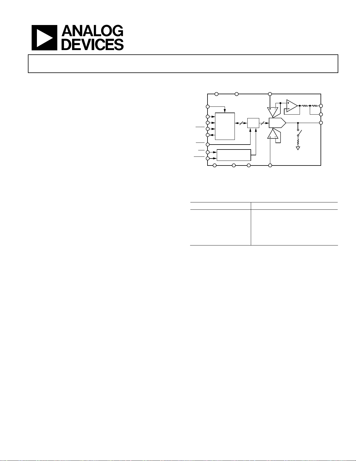
FUNCTIONAL BLOCK DIAGRAM
REFP
6.8kΩ
IOV
SDIN
SCLK
SYNC
SDO
LDAC
CLR
RESET
CC
INPUT
SHIFT
REGIST ER
AND
CONTROL
LOGIC
POWER-ON RESET
AND CLEAR LOGIC
DGND
16
SS
16
V
REFN
Figure 1.
16-BIT
DAC
REG
AGNDV
A1
DAC
Table 1. Related Devices
Part No. Description
AD5790 20-bit, 2 LSB accurate DAC
AD5791 20-bit, 1 LSB accurate DAC
AD5780 18-bit, 1 LSB accurate DAC
AD5781 18-bit, 0.5 LSB INL
AD5541A/AD5542A 16-bit, 1 LSB accurate 5 V DAC
PRODUCT HIGHLIGHTS
1. True 16-bit accuracy.
2. Wide power supply range of up to ±16.5 V.
3. −40°C to +125°C operating temperature range.
4. Low 8 nV/√Hz noise.
5. Low ±0.018 ppm/°C gain error temperature coefficient.
COMPANION PRODUCTS
Output Amplifier Buffer: AD8675, ADA4898-1, ADA4004-1
External Reference: ADR445
DC-to-DC Design Tool: ADIsimPower™
Additional companion products on the AD5780 product page
6.8kΩ
R1 R
6kΩ
AD5760
FB
R
INV
V
FB
OUT
09650-001
Rev. B
Information furnished by Analog Devices is believed to be accurate and reliable. However, no
responsibility is assumed by Analog Devices for its use, nor for any infringements of patents or other
rights of third parties that may result from its use. Specifications subject to change without notice. No
license is granted by implication or otherwise under any patent or patent rights of Analog Devices.
Trademarks and registered trademarks are the property of their respective owners.
One Technology Way, P.O. Box 9106, Norwood, MA 02062-9106, U.S.A.
Tel: 781.329.4700 www.analog.com
Fax: 781.461.3113 ©2011-2012 Analog Devices, Inc. All rights reserved.

AD5760 Data Sheet
TABLE OF CONTENTS
Features.............................................................................................. 1
Applications....................................................................................... 1
Functional Block Diagram ..............................................................1
General Description......................................................................... 1
Product Highlights........................................................................... 1
Companion Products....................................................................... 1
Revision History ...............................................................................2
Specifications..................................................................................... 3
Timing Characteristics ................................................................ 5
Absolute Maximum Ratings............................................................ 8
ESD Caution.................................................................................. 8
Pin Configuration and Function Descriptions............................. 9
Typical Performance Characteristics........................................... 11
Terminology .................................................................................... 19
Theory of Operation ......................................................................20
DAC Architecture....................................................................... 20
Serial Interface............................................................................ 20
Hardware Control Pins.............................................................. 21
On-Chip Registers...................................................................... 22
AD5760 Features............................................................................ 25
Power-On to 0 V......................................................................... 25
Configuring the AD5760 .......................................................... 25
DAC Output State ...................................................................... 25
Output Amplifier Configuration.............................................. 25
Applications Information.............................................................. 27
Typical Operating Circuit ......................................................... 27
Evaluation Board........................................................................ 28
Outline Dimensions....................................................................... 29
Ordering Guide .......................................................................... 29
REVISION HISTORY
2/12—Rev. A to Rev. B
Deleted Linearity Compensation Section ..................................... 3
12/11—Rev. 0 to Rev. A
Changes to Table 2............................................................................ 3
Changes to Figure 48...................................................................... 18
Changes to DAC Register Section................................................ 22
Changes to Table 10 and Table 11 ................................................ 23
11/11—Revision 0: Initial Version
Rev. B | Page 2 of 32

Data Sheet AD5760
SPECIFICATIONS
VDD = +12.5 V to +16.5 V, VSS = −16.5 V to −12.5 V, V
R
= unloaded, CL = unloaded, T
L
MIN
to T
, unless otherwise noted.
MAX
= +10 V, V
REFP
= −10 V, VCC = 2.7 V to 5.5 V, IOVCC = 1.71 V to 5.5 V,
REFN
Table 2.
A, B Versions
1
Parameter Min Typ Max Unit Test Conditions/Comments
STATIC PERFORMANCE2
Resolution 16 Bits
Integral Nonlinearity Error (Relative
−0.5 +0.5 LSB B grade, V
= ±10 V, +10 V and +5 V
REFx
Accuracy)
−2 +2 LSB A grade, V
Differential Nonlinearity Error −0.5 +0.5 LSB B grade, V
−1 +1 LSB A grade, V
= ±10 V, +10 V and +5 V
REFx
= ±10 V, +10 V and +5 V
REFx
= ±10 V, +10 V and +5 V
REFx
Long-Term Linearity Error Stability3 0.00625 LSB After 750 hours at TA = 135°C
Full-Scale Error −0.75 ±0.2 +0.75 LSB V
−1.4 ±0.17 +1.4 LSB V
−2.5 ±0.1 +2.5 LSB V
Full-Scale Error Temperature
±0.026 ppm/°C V
= +10 V, V
REFP
= 10 V, V
REFP
= 5 V, V
REFP
= +10 V, V
REFP
REFN
REFN
= −10 V
REFN
= 0 V
= 0 V
REFN
= −10 V
Coefficient
Zero-Scale Error −1.2 ±0.0812 +1.2 LSB V
−2.5 ±0.044 +2.5 LSB V
−5.2 ±0.056 +5.2 LSB V
Zero-Scale Error Temperature
±0.025 ppm/°C V
= +10 V, V
REFP
= 10 V, V
REFP
= 5 V, V
REFP
= +10 V, V
REFP
REFN
REFN
REFN
REFN
= −10 V
= 0 V
= 0 V
= −10 V
Coefficient
Gain Error −19 ±2.3 +19 ppm FSR V
−35 ±1.9 +35 ppm FSR V
−68 ±0.9 +68 ppm FSR V
Gain Error Temperature Coefficient ±0.018 ppm/°C V
= +10 V, V
REFP
= 10 V, V
REFP
= 5 V, V
REFP
= +10 V, V
REFP
REFN
REFN
REFN
REFN
= −10 V
= 0 V
= 0 V
= −10 V
R1, RFB Matching 0.015 %
OUTPUT CHARACTERISTICS
Output Voltage Range V
Output Voltage Settling Time 2.5 μs
V
REFN
REFP
V
10 V step to 0.02%, using the ADA4898-1
buffer in unity-gain mode
3.5 μs 125 code step to ±1 LSB4
Output Noise Spectral Density 8 nV/√Hz At 1 kHz, DAC code = midscale
8 nV/√Hz At 10 kHz, DAC code = midscale
Output Voltage Noise 1.1 μV p-p
DAC code = midscale, 0.1 Hz to 10 Hz
bandwidth
Midscale Glitch Impulse4 14 nV-sec V
3.5 nV-sec V
4 nV-sec V
MSB Segment Glitch Impulse4 14 nV-sec V
3.5 nV-sec V
4 nV-sec V
= +10 V, V
REFP
= 10 V, V
REFP
= 5 V, V
REFP
= +10 V, V
REFP
= 10 V, V
REFP
= 5 V, V
REFP
= −10 V
REFN
= 0 V
REFN
= 0 V
REFN
= −10 V, see Figure 43
REFN
= 0 V, see Figure 44
REFN
= 0 V, see Figure 45
REFN
Output Enabled Glitch Impulse 57 nV-sec On removal of output ground clamp
Digital Feedthrough 0.27 nV-sec
DC Output Impedance (Normal
3.4 kΩ
Mode)
DC Output Impedance (Output
6 kΩ
Clamped to Ground)
Rev. B | Page 3 of 32

AD5760 Data Sheet
A, B Versions
1
Parameter Min Typ Max Unit Test Conditions/Comments
REFERENCE INPUTS
V
Input Range 5 VDD − 2.5 V
REFP
V
Input Range VSS + 2.5 0 V
REFN
Input Bias Current −20 −0.63 +20 nA
−4 −0.63 +4 TA = 0°C to 105°C
Input Capacitance 1 pF V
REFP
, V
REFN
LOGIC INPUTS
Input Current5 −1 +1 μA
Input Low Voltage, VIL 0.3 × IOVCC V IOVCC = 1.71 V to 5.5 V
Input High Voltage, VIH 0.7 × IOVCC V IOVCC = 1.71 V to 5.5 V
Pin Capacitance 5 pF
LOGIC OUTPUT (SDO)
Output Low Voltage, VOL 0.4 V IOVCC = 1.71 V to 5.5 V, sinking 1 mA
Output High Voltage, VOH IOVCC − 0.5 V IOVCC = 1.71 V to 5.5 V, sourcing 1 mA
High Impedance Leakage Current ±1 μA
High Impedance Output
3 pF
Capacitance
POWER REQUIREMENTS All digital inputs at DGND or IOVCC
VDD 7.5 VSS + 33 V
VSS V
− 33 −2.5 V
DD
VCC 2.7 5.5 V
IOVCC 1.71 5.5 V IOVCC ≤ VCC
IDD 10.3 14 mA
ISS −10 −14 mA
ICC 600 900 μA
IOICC 52 140 μA SDO disabled
DC Power Supply Rejection Ratio ±7.5 μV/V ∆VDD ± 10%, VSS = −15 V
±1.5 μV/V ∆VSS ± 10%, VDD = 15 V
AC Power Supply Rejection Ratio 90 dB ∆VDD ± 200 mV, 50 Hz/60 Hz, VSS = −15 V
90 dB ∆VSS ± 200 mV, 50 Hz/60 Hz, VDD = 15 V
1
Temperature range: −40°C to +125°C, typical conditions: TA = 25°C, VDD = +15 V, VSS = −15 V, V
2
Performance characterized with the AD8675ARZ output buffer.
3
Linearity error refers to both INL error and DNL error; either parameter can be expected to drift by the amount specified after the length of time specified.
4
The AD5760 is configured in unity-gain mode with a low-pass RC filter on the output. R = 300 Ω, C = 143 pF (total capacitance seen by the output buffer, lead
capacitance, and so forth).
5
Current flowing in an individual logic pin.
= +10 V, V
REFP
= −10 V.
REFN
Rev. B | Page 4 of 32
Data Sheet AD5760
TIMING CHARACTERISTICS
VCC = 2.7 V to 5.5 V; all specifications T
Table 3.
Parameter
2
t
40 28 ns min SCLK cycle time
1
IOVCC = 1.71 V to 3.3 V IOVCC = 3.3 V to 5.5 V
92 60 ns min SCLK cycle time (readback and daisy-chain modes)
t2 15 10 ns min SCLK high time
t3 9 5 ns min SCLK low time
t4 5 5 ns min
t5 2 2 ns min
t6 48 40 ns min
t7 8 6 ns min
t8 9 7 ns min Data setup time
t9 12 7 ns min Data hold time
t10 13 10 ns min
t11 20 16 ns min
t12 14 11 ns min
t13 130 130 ns typ
t14 130 130 ns typ
t15 50 50 ns min
t16 140 140 ns typ
t17 0 0 ns min
t18 65 60 ns max
t19 62 45 ns max SCLK rising edge to SDO valid (CL = 50 pF)
t20 0 0 ns min
t21 35 35 ns typ
t22 150 150 ns typ
1
All input signals are specified with tR = tF = 1 ns/V (10% to 90% of IOVCC) and timed from a voltage level of (VIL + VIH)/2.
2
Maximum SCLK frequency is 35 MHz for write mode and 16 MHz for readback and daisy-chain modes.
MIN
Limit1
to T
, unless otherwise noted.
MAX
Unit Test Conditions/Comments
to SCLK falling edge setup time
SYNC
SCLK falling edge to SYNC
Minimum SYNC
rising edge to next SCLK falling edge ignore
SYNC
falling edge to SYNC falling edge
LDAC
rising edge to LDAC falling edge
SYNC
pulse width low
LDAC
falling edge to output response time
LDAC
rising edge to output response time (LDAC tied low)
SYNC
pulse width low
CLR
pulse activation time
CLR
falling edge to first SCLK rising edge
SYNC
rising edge to SDO tristate (CL = 50 pF)
SYNC
rising edge to SCLK rising edge ignore
SYNC
pulse width low
RESET
pulse activation time
RESET
high time
rising edge hold time
Rev. B | Page 5 of 32
AD5760 Data Sheet
SCLK
t
t
9
t
15
16
SYNC
SDIN
LDAC
V
OUT
V
OUT
CLR
t
6
t
4
t
8
DB23 DB0
t
10
t
t
1
3
t
2
t
7
2421
t
5
t
t
11
t
14
12
t
13
SCLK
SYNC
SDIN
SDO
V
OUT
RESET
V
OUT
t
21
t
22
09650-002
Figure 2. Write Mode Timing Diagram
t
t
17
t
6
t
4
t
t
8
DB23 DB0
9
INPUT WORD SPECIFIES
REGISTE R TO BE READ
t
1
t
3
t
2
t
7
24221241
t
t
5
17
NOP CONDI TION
DB23 DB0
REGISTER CONTENTS CLOCKED OUT
t
19
20
t
5
t
18
09650-003
Figure 3. Readback Mode Timing Diagram
Rev. B | Page 6 of 32
Data Sheet AD5760
t
20
t
5
t
18
09650-004
SCLK
SYNC
SDIN
SDO
t
t
17
12 24 4825
t
6
t
4
t
8
DB23
INPUT WORD FOR DAC N
DB23
t
3
t
9
UNDEFINED
1
26
t
2
DB0 DB23 DB0
INPUT WORD FOR DAC N – 1
t
19
DB0 DB23 DB0
INPUT WORD FOR DAC N
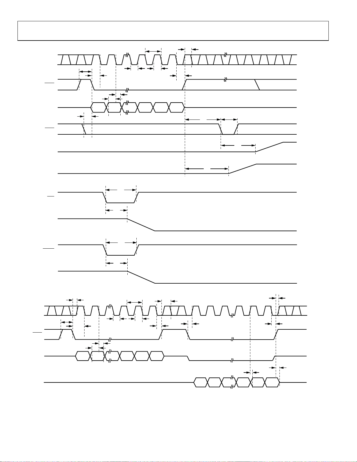
Figure 4. Daisy-Chain Mode Timing Diagram
Rev. B | Page 7 of 32
AD5760 Data Sheet
ABSOLUTE MAXIMUM RATINGS
TA = 25°C, unless otherwise noted. Transient currents of up to
100 mA do not cause SCR latch-up.
Table 4.
Parameter Rating
VDD to AGND −0.3 V to +34 V
VSS to AGND −34 V to +0.3 V
VDD to VSS −0.3 V to +34 V
VCC to DGND −0.3 V to +7 V
IOVCC to DGND
Digital Inputs to DGND
V
to AGND −0.3 V to VDD + 0.3 V
OUT
V
to AGND −0.3 V to VDD + 0.3 V
REFP
V
to AGND VSS − 0.3 V to +0.3 V
REFN
DGND to AGND −0.3 V to +0.3 V
Operating Temperature Range, TA
Industrial −40°C to +125°C
Storage Temperature Range −65°C to +150°C
Maximum Junction Temperature,
max
T
J
Power Dissipation (TJ max − TA)/θJA
LFCSP Package
θJA Thermal Impedance 31.0°C/W
Lead Temperature JEDEC industry standard
Soldering J-STD-020
ESD (Human Body Model) 1.6 kV
−0.3 V to V
(whichever is less)
−0.3 V to IOV
+7 V (whichever is less)
150°C
+ 3 V or +7 V
CC
+ 0.3 V or
CC
Stresses above those listed under Absolute Maximum Ratings
may cause permanent damage to the device. This is a stress
rating only; functional operation of the device at these or any
other conditions above those indicated in the operational
section of this specification is not implied. Exposure to absolute
maximum rating conditions for extended periods may affect
device reliability.
This device is a high performance integrated circuit with an
ESD rating of 1.6 kV, and it is ESD sensitive. Proper precautions
must be taken for handling and assembly.
ESD CAUTION
Rev. B | Page 8 of 32
Data Sheet AD5760
2
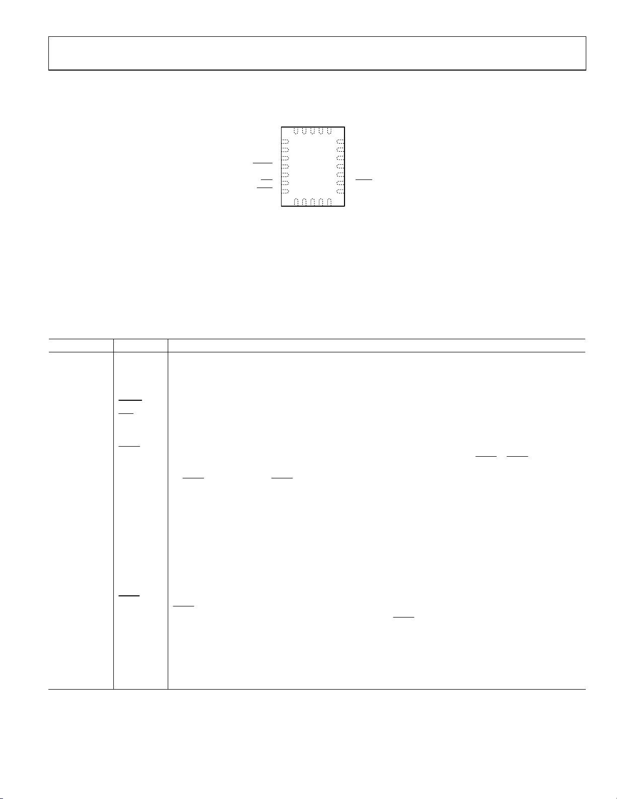
PIN CONFIGURATION AND FUNCTION DESCRIPTIONS
DNC
23
DNC
22
DNC
21
FB
R
20
INV
24
V
1
OUT
V
2
REFP
V
3
DD
RESET
V
DD
CLR
LDAC
NOTES
1. DNC = DO NOT CONNECT
. NEGATIVE ANALOG SUPPLY CONN
A VOLTAGE IN THE RANGE OF –
AN BE CONNECTED. V
C
TO AGND. THE PADDLE CAN BE LEFT E
UNCONNE
CONNECTION IS MA
RECOMMENDED THAT THE
CONNECTED TO A COPPER PLANE FO
CTED PROVIDED THAT A SUP
AL PERFORMANCE.
THERM
AD5760
4
TOP VIEW
5
(Not to Scale)
6
7
8
9
11
10
CCVCC
SDO
DNC
IOV
. DO NOT CONNECT TO THIS PIN.
SHOULD BE DEC
SS
DE AT THE V
PADDLE BE THERMALLY
AGND
19
V
18
SS
V
17
SS
V
16
REFN
15
DGND
14
SYNC
13
SCLK
12
SDIN
ECTION (V
16.5 V TO –2.5 V
PINS. IT IS
SS
SS
OUPLED
LECTRICALLY
PLY
R ENHANCED
).
09650-005
Figure 5. Pin Configuration
Table 5. Pin Function Descriptions
Pin No. Mnemonic Description
1 V
2 V
3, 5 VDD
Analog Output Voltage.
OUT
Positive Reference Voltage Input. A voltage in the range of 5 V to VDD − 2.5 V can be connected to this pin.
REFP
Positive Analog Supply Connection. A voltage in the range of 7.5 V to 16.5 V can be connected to this pin.
VDD must be decoupled to AGND.
4
6
RESET
Active Low Input. Asserting this pin sets the DAC register to a user defined value (see Table 12) and updates
CLR
Active Low Reset. Asserting this pin returns the AD5760 to its power-on status.
the DAC output. The output value depends on the DAC register coding that is being used, either binary or
twos complement.
7
Active Low Load DAC Logic Input. This pin is used to update the DAC register and, consequently, the analog
LDAC
output. When tied permanently low, the output is updated on the rising edge of SYNC
during the write cycle, the input register is updated, but the output update is held off until the falling edge
of LDAC
. Do not leave the LDAC pin unconnected.
8 VCC Digital Supply. Voltage range is from 2.7 V to 5.5 V. VCC should be decoupled to DGND.
9 IOVCC
Digital Interface Supply. Digital threshold levels are referenced to the voltage applied to this pin. Voltage
range is from 1.71 V to 5.5 V.
10, 21, 22, 23 DNC Do Not Connect. Do not connect to these pins.
11 SDO Serial Data Output.
12 SDIN
Serial Data Input. This device has a 24-bit input shift register. Data is clocked into the register on the falling
edge of the serial clock input.
13 SCLK
Serial Clock Input. Data is clocked into the input shift register on the falling edge of the serial clock input.
Data can be transferred at rates of up to 35 MHz.
14
Level Triggered Control Input (Active Low). This is the frame synchronization signal for the input data. When
SYNC
SYNC
goes low, it enables the input shift register, and data is then transferred in on the falling edges of the
following clocks. The DAC is updated on the rising edge of SYNC
.
15 DGND Ground Reference Pin for Digital Circuitry.
16 V
17, 18 VSS
Negative Reference Voltage Input.
REFN
Negative Analog Supply Connection. A voltage in the range of −16.5 V to −2.5 V can be connected to this
must be decoupled to AGND.
pin. V
SS
19 AGND Ground Reference Pin for Analog Circuitry.
. If LDAC is held high
Rev. B | Page 9 of 32

AD5760 Data Sheet
Pin No. Mnemonic Description
20 RFB Feedback Connection for External Amplifier. See the AD5760 Features section for further details.
24 INV Inverting Input Connection for External Amplifier. See the AD5760 Features section for further details.
EPAD VSS
Negative Analog Supply Connection (V
this pin. V
must be decoupled to AGND. The paddle can be left electrically unconnected provided that a
SS
supply connection is made at the V
copper plane for enhanced thermal performance.
). A voltage in the range of −16.5 V to −2.5 V can be connected to
SS
pins. It is recommended that the paddle be thermally connected to a
SS
Rev. B | Page 10 of 32

Data Sheet AD5760
TYPICAL PERFORMANCE CHARACTERISTICS
0.10
V
= +10V
REFP
V
= –10V
REFN
0.08
V
= +15V
DD
V
= –15V
SS
0.06
0.04
0.02
0
INL (LSB)
–0.02
–0.04
–0.06
–0.08
–0.10
0 10000 20000 30000 40000 50000 60000 70000
AD8675 OUTPUT BUFF ER
T
= 25°C
A
DAC CODE
Figure 6. Integral Nonlinearity Error vs. DAC Code, ±10 V Span
0.15
V
= +10V
REFP
= 0V
V
REFN
= +15V
V
DD
= –15V
V
SS
0.10
0.05
INL (LSB)
0
–0.05
AD8675 OUTPUT BUFFER
= 25°C
T
–0.10
0 10000 20000 30000 40000 50000 60000 70000
DAC CODE
A
Figure 7. Integral Nonlinearity Error vs. DAC Code, 10 V Span
0.10
V
= +5V
REFP
= 0V
V
REFN
= +15V
V
DD
= –15V
V
0.05
SS
09650-006
09650-007
0.10
V
= +5V
REFP
= 0V
V
REFN
= +15V
V
DD
= –15V
V
0.05
SS
0
–0.05
INL (LSB)
–0.10
–0.15
AD8675 OUTPUT BUF FER
= 25°C
T
–0.20
0 10000 20000 30000 40000 50000 60000 70000
DAC CODE
A
Figure 9. Integral Nonlinearity Error vs. DAC Code, 5 V Span, ×2 Gain Mode
0.10
0.08
0.06
0.04
0.02
0
DNL (LSB)
–0.02
–0.04
–0.06
–0.08
–0.10
0 10000 20000 30000 40000 50000 60000 70000
AD8675 OUTPUT BUFFER
T
A
DAC CODE
= 25°C
V
V
V
V
REFP
REFN
DD
SS
= +10V
= –10V
= +15V
= –15V
09650-010
Figure 10. Differential Nonlinearity Error vs. DAC Code, ±10 V Span
0.20
V
= +10V
REFP
= 0V
V
REFN
= +15V
V
DD
0.15
= –15V
V
SS
09650-009
0
–0.05
INL (LSB)
–0.10
–0.15
AD8675 OUTPUT BUFFER
= 25°C
T
–0.20
0 10000 20000 30000 40000 50000 60000 70000
DAC CODE
A
Figure 8. Integral Nonlinearity Error vs. DAC Code, 5 V Span
09650-008
Rev. B | Page 11 of 32
0.10
0.05
DNL (LSB)
0
–0.05
AD8675 OUTPUT BUFFE R
T
= 25°C
–0.10
0 10000 20000 30000 40000 50000 60000 70000
DAC CODE
A
Figure 11. Differential Nonlinearity Error vs. DAC Code, 10 V Span
09650-011

AD5760 Data Sheet
0.10
0.08
0.06
0.04
0.02
0
DNL (LSB)
–0.02
–0.04
–0.06
–0.08
AD8675 OUTPUT BUFFER
= 25°C
T
A
–0.10
0 10000 20000 30000 40000 50000 60000 70000
DAC CODE
V
V
V
V
REFP
REFN
DD
SS
= +5V
= 0V
= +15V
= –15V
Figure 12. Differential Nonlinearity Error vs. DAC Code, 5 V Span
09650-012
0.09
VDD = +15V
V
= –15V
SS
AD8675 OUTPUT BUFFER
0.07
0.05
DNL ERROR (LSB)
0.03
0.01
–0.01
–40
±10V SPAN MAX INL
+10V SPAN MAX INL
+5V SPAN MAX INL
–200 20406080100
±10V SPAN MIN INL
+10V SPAN MIN I NL
+5V SPAN MIN INL
TEMPERATURE (°C)
Figure 15. Differential Nonlinearity Error vs. Temperature
09650-014
AD8675 OUTPUT BUF FER
0.09
T
= 25°C
A
0.07
0.05
0.03
DNL (LSB)
0.01
–0.01
V
= +5V
REFP
V
–0.03
–0.05
0 10000 20000 30000 40000 50000 60000 70000
DAC CODE
V
V
REFN
DD
SS
= 0V
= +15V
= –15V
Figure 13. Differential Nonlinearity Error vs. DAC Code, 5 V Span,
×2 Gain Mode
0.20
VDD = +15V
V
= –15V
SS
AD8675 OUTPUT BUFFER
0.15
0.10
0.05
INL ERROR (LSB)
0
–0.05
–0.10
±10V SPAN MAX INL
+10V SPAN MAX INL
+5V SPAN MAX INL
±10V SPAN MIN INL
+10V SPAN MIN I NL
+5V SPAN MIN I NL
0.08
0.06
0.04
0.02
TA = 25°C
0
V
= +10V
REFP
V
= –10V
REFN
–0.02
AD8675 OUTPUT BUF FER
INL ERROR (LSB)
–0.04
–0.06
–0.08
–0.1.0
09650-013
12.5 13.0 13.5 14.0 14. 5 15.0 15.5 16.0 16.5
INL MAX
INL MIN
VDD/|VSS| (V)
09650-016
Figure 16. Integral Nonlinearity Error vs. Supply Voltage, ±10 V Span
0.15
0.10
0.05
TA = 25°C
V
0
REFP
V
REFN
AD8675 OUTPUT BUFFER
INL ERROR (LSB)
–0.05
–0.10
= 5V
= 0V
INL MAX
INL MIN
–0.15
–40 –20 0 20 40 60 80 100
TEMPERATURE (°C)
Figure 14. Integral Nonlinearity Error vs. Temperature
09650-015
Rev. B | Page 12 of 32
–0.15
7.5 8.5 9. 5 10.5 11.5 12.5 13.5 14.5 15.5 16.5
VDD/|VSS| (V)
Figure 17. Integral Nonlinearity Error vs. Supply Voltage, 5 V Span
09650-017

Data Sheet AD5760
–
0.09
0.08
0.07
0.06
TA = 25°C
DNL ERROR (LSB)
0.05
0.04
0.03
0.02
0.01
–0.01
= +10V
V
REFP
= –10V
V
REFN
AD8675 OUTPUT BUF FER
0
12.5 13.0 13.5 14. 0 14.5 15.0 15.5 16.0 16.5
DNL MAX
DNL MIN
VDD/|VSS| (V)
Figure 18. Differential Nonlinearity Error vs. Supply Voltage, ±10 V Span
0.09
0.08
0.07
0.06
0.05
TA = 25°C
= 5V
V
REFP
0.04
0.03
DNL ERROR (LSB)
0.02
0.01
–0.01
= 0V
V
REFN
AD8675 OUTPUT BUFFER
0
7.5 8. 5 9.5 10.5 11.5 12. 5 13.5 14.5 15.5 16.5
DNL MAX
DNL MIN
VDD/|VSS| (V)
Figure 19. Differential Nonlinearity Error vs. Supply Voltage, 5 V Span
0.8
TA = 25°C
= 5V
V
REFP
= 0V
V
REFN
0.6
AD8675 OUTPUT BUFF ER
0.4
0.2
0
ZERO-SCALE ERROR (LSB)
–0.2
–0.4
7.5 8.5 9.5 10.5 11.5 12.5 13.5 14. 5 15.5 16. 5
09650-018
VDD/|VSS| (V)
09650-021
Figure 21. Zero-Scale Error vs. Supply Voltage, 5 V Span
0.02
–0.03
–0.04
–0.05
–0.06
–0.07
–0.08
–0.09
MIDSCALE ERROR (LSB)
–0.10
TA = 25°C
V
= +10V
REFP
–0.11
V
= –10V
REFN
AD8675 OUTPUT BUFFE R
–0.12
12.5 13.0 13.5 14.0 14. 5 15.0 15. 5 16.0 16. 5
09650-019
VDD/|VSS| (V)
09650-022
Figure 22. Midscale Error vs. Supply Voltage, ±10 V Span
0.15
TA = 25°C
V
= +10V
REFP
V
= –10V
REFN
AD8675 OUTPUT BUF FER
0.10
0.05
0
ZERO-SCAL E ERROR (LS B)
–0.05
–0.10
12.5 13.0 13.5 14. 0 14.5 15.0 15.5 16.0 16.5
VDD/|VSS| (V)
Figure 20. Zero-Scale Error vs. Supply Voltage, ±10 V Span
09650-020
Rev. B | Page 13 of 32
0.5
0.4
0.3
0.2
0.1
0
–0.1
–0.2
MIDSCALE ERRO R (LSB)
–0.3
TA = 25°C
= 5V
V
REFP
–0.4
–0.5
= 0V
V
REFN
AD8675 OUTPUT BUF FER
7.5 8.5 9.5 10.5 11.5 12.5 13. 5 14.5 15. 5 16.5
VDD/|VSS| (V)
Figure 23. Midscale Error vs. Supply Voltage, 5 V Span
09650-023

AD5760 Data Sheet
0.14
TA = 25°C
V
REFP
V
0.12
REFN
AD8675 OUTPUT BUFF ER
0.10
0.08
0.06
0.04
FULL-SCALE ERROR (LSB)
0.02
= +10V
= –10V
0.38
TA = 25°C
V
= 5V
REFP
= 0V
V
REFN
0.36
AD8675 OUTPUT BUFFER
0.34
0.32
0.30
GAIN ERRO R (LSB)
0.28
0
12.5 13.
0 13.5 14.0 1 4.5 15.0 15. 5 16.0 16.5
VDD/|VSS| (V)
Figure 24. Full-Scale Error vs. Supply Voltage, ±10 V Span
0.5
TA = 25°C
= 5V
V
REFP
V
0.3
0.1
–0.1
–0.3
–0.5
FULL-SCALE ERROR (LSB)
–0.7
–0.9
= 0V
REFN
AD8675 OUTPUT BUFF ER
7.5 8.5 9.5 10.5 11.5 12.5 13.5 14.5 15.5 16.5
VDD/|VSS| (V)
Figure 25. Full-Scale Error vs. Supply Voltage, 5 V Span
0.10
TA = 25°C
= +10V
V
REFP
= –10V
V
0.08
REFN
AD8675 OUTPUT BUF FER
0.06
0.04
0.02
0
GAIN ERROR ( LSB)
–0.02
–0.04
0.26
09650-024
7.5 8.5 9.5 10.5 11.5 12.5 13.5 14.5 15.5 16.5
VDD/|VSS| (V)
09650-027
Figure 27. Gain Error vs. Supply Voltage, 5 V Span
0.08
0.06
0.04
0.02
TA = 25°C
V
= +15V
DD
0
V
= –15V
SS
AD8675 OUTPUT BUFFER
–0.02
INL ERROR (LSB)
–0.04
–0.06
–0.08
–0.10
5.0 5.5 6.0 6. 5 7. 0 7. 5 8. 0 8. 5 9. 0 9. 5 10.0
09650-025
INL MAX
INL MIN
V
REFP
/|V
| (V)
REFN
09650-028
Figure 28. Integral Nonlinearity Error vs. Reference Voltage
0.08
0.06
TA = 25°C
V
= +15V
0.04
DD
V
= –15V
SS
AD8675 OUTPUT BUFFER
0.02
DNL ERROR (LSB)
0
INL MAX
INL MIN
–0.06
12.5 13.0 13.5 14.0 14.5 15. 0 15.5 16.0 16. 5
VDD/|VSS| (V)
Figure 26. Gain Error vs. Supply Voltage, ±10 V Span
09650-026
Rev. B | Page 14 of 32
–0.02
5.0 5.5 6.0 6.5 7.0 7.5 8.0 8.5 9.0 9. 5 10.0
V
/|V
REFN
| (V)
REFP
Figure 29. Differential Nonlinearity Error vs. Reference Voltage
09650-029

Data Sheet AD5760
–
–
–
0.02
–0.03
–0.04
TA = 25°C
V
= +15V
DD
V
= –15V
SS
AD8675 OUTPUT BUFFER
0.25
–0.30
–0.05
–0.06
–0.07
–0.08
ZERO-SCALE ERRO R (LSB)
–0.09
–0.10
5.05.56.06.57.07.58.08.59.09.510.0
V
/|V
REFN
| (V)
REFP
Figure 30. Zero-Scale Error vs. Reference Voltage
0.05
TA = 25°C
= +15V
V
DD
–0.07
V
= –15V
SS
AD8675 OUTPUT BUFFER
–0.09
–0.11
–0.13
–0.15
–0.17
–0.19
MIDSCALE ERROR (L SB)
–0.21
–0.23
–0.25
5.05.56.06.57.07.58.08.59.09.510.0
V
/|V
REFN
| (V)
REFP
Figure 31. Midscale Error vs. Reference Voltage
–0.35
–0.40
GAIN ERROR (LSB)
–0.45
–0.50
5.05.56.06.57.07.58.08.59.09.510.0
09650-030
V
REFP
TA = 25°C
V
= +15V
DD
V
= –15V
SS
AD8675 OUTPUT BUFFER
/|V
| (V)
REFN
09650-033
Figure 33. Gain Error vs. Reference Voltage
0.50
±10V SPAN
+10V SPAN
+5V SPAN
0.45
0.40
0.35
0.30
0.25
FULL-SCALE ERROR (LSB)
0.20
0.15
–40 –20 0 20 40 60 80 100
09650-031
TEMPERAT URE (°C)
VDD = +15V
= –15V
V
SS
AD8675 OUTPUT BUFFER
09650-034
Figure 34. Full-Scale Error vs. Temperature
0.40
0.38
0.36
0.34
0.32
0.3
0.28
0.26
FULL-SCAL E ERROR (LSB)
0.24
0.22
0.20
5.0 5.5 6.0 6.5 7.0 7.5 8.0 8.5 9.0 9.5 10.0
V
REFP
TA = 25°C
= +15V
V
DD
= –15V
V
SS
AD8675 OUTPUT BUFF ER
/|V
| (V)
REFN
Figure 32. Full-Scale Error vs. Reference Voltage
09650-032
Rev. B | Page 15 of 32
0.15
0.10
0.05
0
–0.05
–0.10
–0.15
MIDSCAL E ERRO R (LSB)
–0.20
VDD = +15V
–0.25
V
= –15V
SS
AD8675 OUTPUT BUFFER
–0.30
–40 –20 0 20 40 60 80 100
TEMPERATURE (°C)
±10V SPAN
+10V SPAN
+5V SPAN
Figure 35. Midscale Error vs. Temperature
09650-035

AD5760 Data Sheet
0.4
±10V SPAN
+10V SPAN
+5V SPAN
0.2
0
–0.2
–0.4
ZERO-SCALE ERROR (LSB)
–0.6
–0.8
–40 –20 0 20 40 60 80 100
TEMPERATURE (°C)
VDD = +15V
= –15V
V
SS
AD8675 OUTPUT BUFFE R
Figure 36. Zero-Scale Error vs. Temperature
09650-036
0.010
0.008
0.006
0.004
0.002
(mA)
0
SS
/I
DD
–0.002
I
–0.004
–0.006
–0.008
–0.010
–20 –15 –10 –5 0 5 10 15 20
I
SS
V
(V)
DD/VSS
Figure 39. Power Supply Currents vs. Power Supply Voltages
I
DD
09650-039
0
±10V SPAN
+10V SPAN
–0.1
+5V SPAN
–0.2
–0.3
–0.4
–0.5
–0.6
GAIN ERROR (LSB)
–0.7
–0.8
–0.9
–1.0
–40 –20 0 20 40 60 80 100
TEMPERATURE (°C)
VDD = +15V
= –15V
V
SS
AD8675 OUTPUT BUFF ER
Figure 37. Gain Error vs. Temperature
900
= 25°C
T
A
800
700
600
500
(µA)
CC
400
IOI
300
200
100
0
01
23456
LOGIC INPUT VOLTAGE (V)
Figure 38. IOI
IOVCC = 5V, LOGIC VOLTAGE
INCREASI NG
= 5V, LOGIC VOLTAGE
IOV
CC
DECREASING
= 3V, LOGIC VOLTAGE
IOV
CC
INCREASI NG
= 3V, LOGIC VOLTAGE
IOV
CC
DECREASING
vs. Logic Input Voltage
CC
6
4
2
0
(V)
–2
OUT
V
–4
–6
–8
–10
–1012345
09650-037
TIME (µs)
VDD = +15V
= –15V
V
SS
= +10V
V
REFP
= –10V
V
REFN
ADA4808-1 BUFFERED
LOAD = 10MΩ || 20pF
09650-040
Figure 40. Rising Full-Scale Voltage Step
6
4
2
0
(V)
–2
OUT
V
–4
–6
–8
–10
–1012345
09650-038
TIME (µs)
VDD = +15V
= –15V
V
SS
= +10V
V
REFP
= –10V
V
REFN
ADA4808-1 BUFFERED
LOAD = 10MΩ || 20pF
09650-041
Figure 41. Falling Full-Scale Voltage Step
Rev. B | Page 16 of 32

Data Sheet AD5760
10
9
8
7
6
(mV)
5
OUT
V
4
3
V
2
1
0
–1012345
TIME (µs)
= +10V
REFP
= –10V
V
REFN
RC LOW-PASS FILTER
UNITY-GAIN MODE
ADA4898-1
Figure 42. 500 Code Step Settling Time
09650-042
6
V
= 5V
REFP
= 0V
V
REFN
UNITY-GAIN MODE
ADA4898-1
5
RC LOW -PASS FIL TER
4
3
2
OUTPUT GLITCH (nV-s)
1
0
16384
65536
114688
163840
212992
262144
311296
360448
409600
458752
507904
557056
CODE
Figure 45. 6 MSB Segment Glitch Energy for 5 V V
606208
655360
704512
753664
802816
NEGATIVE
POSITIVE
851968
901120
950272
REF
999424
09650-046
25
V
= +10V
REFP
= –10V
V
REFN
UNITY-GAIN MODE
ADA4898-1
20
RC LOW PASS FILTER
15
10
OUTPUT G LITCH (nV-s)
5
0
16384
49152
81920
114688
147456
180224
212992
245760
278528
311296
344064
376832
409600
442368
NEGATIVE
CODE CHANGE
475136
507904
540672
573440
606208
638976
CODE
Figure 43. 6 MSB Segment Glitch Energy for ±10 V V
4.0
V
= 10V
REFP
V
= 0V
REFN
3.5
UNITY-GAIN MODE
ADA4898-1
RC LOW-PASS FILTER
3.0
2.5
2.0
1.5
OUTPUT G LIT CH (nV-s)
1.0
0.5
CODE CHANGE
671744
704512
737280
770048
NEGATIVE
POSITIVE
POSITIVE
802816
835584
868352
901120
NEGATIV E
POSITIVE
933888
REF
55
45
35
25
15
5
OUTPUT GLIT CH (V)
–5
–15
–25
–10123
966656
999424
1032192
09650-044
TIME (µs)
±10V REF
10V REF
5V REF
09650-047
Figure 46. Midscale Peak-to-Peak Glitch for ±10 V
800
OUTPUT VOLTAGE (nV)
600
400
200
–200
–400
TA = 25°C
V
V
V
V
0
DD
SS
REFP
REFN
= +15V
= –15V
= +10V
= –10V
MIDSCALE CODE L OADED
OUTPUT UNBUFF ERED
AD8676 REFERENCE BUFF ERS
0
16384
65536
114688
163840
212992
262144
311296
360448
409600
458752
507904
557056
606208
655360
704512
CODE
753664
Figure 44. 6 MSB Segment Glitch Energy for 10 V V
–600
012345678 910
802816
851968
901120
950272
999424
09650-045
REF
Figure 47. Voltage Output Noise, 0.1 Hz to 10 Hz Bandwidth
TIME (Seconds)
09650-048
Rev. B | Page 17 of 32

AD5760 Data Sheet
√
100
Hz)
10
NSD (nV/
1
0.1 1 10 100 1k 10k
FREQUENC Y (Hz)
Figure 48. Noise Spectral Density vs. Frequency
VDD = +15V
= –15V
V
SS
V
= +10V
REFP
V
= –10V
REFN
09650-056
0.20
0.18
0.16
0.14
0.12
0.10
0.08
0.06
OUTPUT VOLTAGE (V)
0.04
0.02
0
–0.02
0123
TIME (µs)
456
Figure 49. Glitch Impulse on Removal of Output Clamp
VDD = +15V
V
= –15V
SS
V
= +10V
REFP
V
= –10V
REFN
UNITY GAIN
ADA4898-1
09650-049
Rev. B | Page 18 of 32

Data Sheet AD5760
TERMINOLOGY
Relative Accuracy
Relative accuracy, or integral nonlinearity (INL), is a measure of
the maximum deviation, in LSB, from a straight line passing
through the endpoints of the DAC transfer function. A typical
INL error vs. code plot is shown in Figure 6.
Differential Nonlinearity (DNL)
Differential nonlinearity is the difference between the measured
change and the ideal 1 LSB change between any two adjacent
codes. A specified differential nonlinearity of ±1 LSB maximum
ensures monotonicity. This DAC is guaranteed monotonic. A
typical DNL error vs. code plot is shown in Figure 10.
Linearity Error Long-Term Stability
Linearity error long-term stability is a measure of the stability of
the linearity of the DAC over a long period of time. It is specified
in LSB for a time period of 500 hours and 1000 hours at an
elevated ambient temperature.
Zero-Scale Error
Zero-scale error is a measure of the output error when zero-scale
code (0x00000) is loaded to the DAC register. Ideally, the output
voltage should be V
. Zero-scale error is expressed in LSBs.
REFN
Zero-Scale Error Temperature Coefficient
Zero-scale error temperature coefficient is a measure of the
change in zero-scale error with a change in temperature. It is
expressed in ppm FSR/°C.
Full-Scale Error
Full-scale error is a measure of the output error when full-scale
code (0x3FFFF) is loaded to the DAC register. Ideally, the
output voltage should be V
− 1 LSB. Full-scale error is
REFP
expressed in LSBs.
Full-Scale Error Temperature Coefficient
Full-scale error temperature coefficient is a measure of the
change in full-scale error with a change in temperature. It is
expressed in ppm FSR/°C.
Gain Error
Gain error is a measure of the span error of the DAC. It is the
deviation in slope of the DAC transfer characteristic from the
ideal, expressed in ppm of the full-scale range.
Gain Error Temperature Coefficient
Gain error temperature coefficient is a measure of the change in
gain error with a change in temperature. It is expressed in ppm
FSR/°C.
Midscale Error
Midscale error is a measure of the output error when midscale
code (0x20000) is loaded to the DAC register. Ideally, the output
voltage should be (V
REFP
– V
REFN
)/2 +V
. Midscale error is
REFN
expressed in LSBs.
Output Voltage Settling Time
Output voltage settling time is the amount of time it takes for
the output voltage to settle to a specified level for a specified
change in voltage. For fast settling applications, a high speed
buffer amplifier is required to buffer the load from the 3.4 kΩ
output impedance of the AD5760, in which case, it is the
amplifier that determines the settling time.
Digital-to-Analog Glitch Impulse
Digital-to-analog glitch impulse is the impulse injected into the
analog output when the input code in the DAC register changes
state. It is specified as the area of the glitch in nV-sec and is
measured when the digital input code is changed by 1 LSB at
the major carry transition (see Figure 49).
Output Enabled Glitch Impulse
Output enabled glitch impulse is the impulse injected into the
analog output when the clamp to ground on the DAC output is
removed. It is specified as the area of the glitch in nV-sec (see
Figure 49).
Digital Feedthrough
Digital feedthrough is a measure of the impulse injected into
the analog output of the DAC from the digital inputs of the
DAC but is measured when the DAC output is not updated. It is
specified in nV-sec and measured with a full-scale code change
on the data bus, that is, from all 0s to all 1s, and vice versa.
Total Harmonic Distortion (THD)
Total harmonic distortion is the ratio of the rms sum of the
harmonics of the DAC output to the fundamental value. Only
the second to fifth harmonics are included.
DC Power Supply Rejection Ratio.
DC power supply rejection ratio is a measure of the rejection of
the output voltage to dc changes in the power supplies applied
to the DAC. It is measured for a given dc change in power
supply voltage and is expressed in μV/V.
AC Power Supply Rejection Ratio (AC PSRR)
AC power supply rejection ratio is a measure of the rejection of
the output voltage to ac changes in the power supplies applied
to the DAC. It is measured for a given amplitude and frequency
change in power supply voltage and is expressed in decibels.
Rev. B | Page 19 of 32

AD5760 Data Sheet
THEORY OF OPERATION
The AD5760 is a high accuracy, fast settling, single, 16-bit,
serial input, voltage output DAC. It operates from a V
voltage of 7.5 V to 16.5 V and a V
supply of −16.5 V to −2.5 V.
SS
Data is written to the AD5760 in a 24-bit word format via a 3-wire
serial interface. The AD5760 incorporates a power-on reset
circuit that ensures the DAC output powers up to 0 V with the
V
pin clamped to AGND through a ~6 kΩ internal resistor.
OUT
DAC ARCHITECTURE
The architecture of the AD5760 consists of two matched DAC
sections. A simplified circuit diagram is shown in Figure 50.
The six MSBs of the 16-bit data-word are decoded to drive
63 switches, E0 to E62. Each of these switches connects one of
63 matched resistors to either the buffered V
voltage. The remaining 10 bits of the data-word drive the
V
REFN
S0 to S9 switches of a 10-bit voltage mode R-2R ladder network.
REFP
supply
DD
or buffered
R
V
V
REFP
REFN
RR
...
2R
2R
2R
...
S12RS9
S0
10-BIT R-2 R LADDER
Figure 50. DAC Ladder Structure Serial Interface
2R
E61
E62
SIX MSBs DECODED INTO
63 EQUAL S EGMENTS
V
OUT
...
2R
2R
...
E0
SERIAL INTERFACE
The AD5760 has a 3-wire serial interface (
SDIN) that is compatible with SPI, QSPI, and MICROWIRE
interface standards, as well as most DSPs (see for a
timing diagram).
Input Shift Register
The input shift register is 24 bits wide. Data is loaded into the
device MSB first as a 24-bit word under the control of a serial
clock input, SCLK, which can operate at up to 35 MHz. The
Table 6
Figure 2
W
bit, three address bits, and
input register consists of a R/
20 data bits as shown in . The timing diagram for this
operation is shown in .
SYNC
Figure 2
, SCLK, and
09650-050
Table 6. Input Shift Register Format
MSB LSB
DB23 DB22 DB21 DB20 DB19 to DB0
R/W
Register address Register data
Table 7. Decoding the Input Shift Register
R/W
Register Address Description
X1 0 0 0 No operation (NOP). Used in readback operations.
0 0 0 1 Write to the DAC register.
0 0 1 0
0 0 1 1
0 1 0 0
1 0 0 1
1 0 1 0
Write to the control register.
Write to the clearcode register.
Write to the software control register.
Read from the DAC register.
Read from the control register.
1 0 1 1 Read from the clearcode register.
1
X is don’t care.
Rev. B | Page 20 of 32

Data Sheet AD5760
Standalone Operation
The serial interface works with both a continuous and noncontinuous serial clock. A continuous SCLK source can be used
SYNC
only if
is held low for the correct number of clock cycles.
In gated clock mode, a burst clock containing the exact number
of clock cycles must be used, and
the final clock to latch the data. The first falling edge of
SYNC
must be taken high after
SYNC
starts the write cycle. Exactly 24 falling clock edges must be applied
to SCLK before
high before the 24
SYNC
is brought high again. If
th
falling SCLK edge, the data written is invalid.
If more than 24 falling SCLK edges are applied before
SYNC
is brought
SYNC
is
brought high, the input data is also invalid.
SYNC
The input shift register is updated on the rising edge of
For another serial transfer to take place,
SYNC
must be brought
.
low again. After the end of the serial data transfer, data is
automatically transferred from the input shift register to the
addressed register. When the write cycle is complete, the output
can be updated by taking
LDAC
low while
SYNC
is high.
Daisy-Chain Operation
For systems that contain several devices, the SDO pin can be
used to daisy chain several devices together. Daisy-chain mode
can be useful in system diagnostics and in reducing the number
of serial interface lines. The first falling edge of
SYNC
starts
the write cycle. SCLK is continuously applied to the input shift
register when
SYNC
is low. If more than 24 clock pulses are
applied, the data ripples out of the shift register and appears on
the SDO line. This data is clocked out on the rising edge of
SCLK and is valid on the falling edge. By connecting the SDO
of the first device to the SDIN input of the next device in the
chain, a multidevice interface is constructed. Each device in the
system requires 24 clock pulses. Therefore, the total number of
clock cycles must equal 24 × N, where N is the total number of
AD5760
devices is complete,
devices in the chain. When the serial transfer to all
SYNC
is taken high. This latches the input
data in each device in the daisy chain and prevents any further
data from being clocked into the input shift register. The serial
clock can be a continuous or a gated clock.
A continuous SCLK source can be used only if
SYNC
is held
low for the correct number of clock cycles. In gated clock mode,
a burst clock containing the exact number of clock cycles must
be used, and
SYNC
must be taken high after the final clock to
latch the data.
In any one daisy-chain sequence, do not mix writes to the DAC
register with writes to any of the other registers. All writes to the
daisy-chained parts must be either writes to the DAC registers
or writes to the control, clearcode, or software control register.
Rev. B | Page 21 of 32
CONTROLL ER
DATA OUT
SERIAL CLOCK
CONTROL O UT
DATA IN
*ADDITIONAL PINS OMITTED F OR CLARIT Y.
Figure 51. Daisy-Chain Block Diagram
Readback
The contents of all the on-chip registers can be read back via
the SDO pin. Tabl e 7 outlines how the registers are decoded.
After a register has been addressed for a read, the next 24 clock
cycles clock the data out on the SDO pin. The clocks must be
applied while
SYNC
is low. When
SDO pin is placed in tristate. For a read of a single register, the
NOP function can be used to clock out the data. Alternatively,
if more than one register is to be read, the data of the first
register to be addressed can be clocked out at the same time
that the second register to be read is being addressed. The SDO
pin must be enabled to complete a readback operation. The
SDO pin is enabled by default.
HARDWARE CONTROL PINS
Load DAC Function (
After data has been transferred into the input register of the
DAC, there are two ways to update the DAC register and DAC
output. Depending on the status of both
of two update modes is selected: synchronous DAC update or
asynchronous DAC update.
Synchronous DAC Update
In this mode,
LDAC
the input shift register. The DAC output is updated on the rising
SYNC
edge of
.
LDAC
)
is held low while data is being clocked into
AD5760*
SDIN
SCLK
SYNC
SDO
SDIN
AD5760*
SCLK
SYNC
SDO
SDIN
AD5760*
SCLK
SYNC
SDO
SYNC
is returned high, the
SYNC
and
LDAC
09650-051
, one

AD5760 Data Sheet
(
−
Asynchronous DAC Update
In this mode,
LDAC
is held high while data is being clocked
into the input shift register. The DAC output is asynchronously
updated by taking
LDAC
low after
The update now occurs on the falling edge of
Reset Function (
RESET
)
SYNC
has been taken high.
LDAC
.
The AD5760 can be reset to its power-on state by two means:
RESET
either by asserting the
in the software control register (see ). If the Table 13
is not used, hardwire it to IOV
Asynchronous Clear Function (
CLR
The
pin is an active low clear that allows the output to be
pin or by using the reset function
RESET
pin
.
CC
)
CLR
cleared to a user defined value. The 16-bit clearcode value is
programmed to the clearcode register (see ). It is
necessary to maintain
CLR
low for a minimum amount of time
to complete the operation (see ). When the Figure 2
is returned high, the output remains at the clear value (if
Table 1 2
CLR
signal
LDAC
Table 8. Hardware Control Pins Truth Table
LDAC CLR
X1 XX1 0 The AD5760 is in reset mode. The device cannot be programmed.
X1 XX1
0 0 1
0 1 1
1 0 1
1
0
1
0
1
X is don’t care.
1 1
0 1
1 1
0 1
RESET
Functio n
1 The DAC register is loaded with the clearcode register value and the output is set accordingly.
1
1 The output remains at the clearcode register value.
1 The output is set according to the DAC register value.
The AD5760 is returned to its power-on state. All registers are set to their default values.
The DAC register is loaded with the clearcode register value, and the output is set accordingly.
The output is set according to the DAC register value.
The DAC register is loaded with the clearcode register value, and the output is set accordingly.
The output is set according to the DAC register value.
The output remains at the clearcode register value.
The output remains set according to the DAC register value.
The output remains at the clearcode register value.
The DAC register is loaded with the clearcode register value and the output is set accordingly.
is high) until a new value is loaded to the DAC register. The
output cannot be updated with a new value while the
CLR
pin is
low. A clear operation can also be performed by setting the CLR
bit in the software control register (see ). Tab le 13
ON-CHIP REGISTERS
DAC Register
Table 9 outlines how data is written to and read from the DAC
register.
The following equation describes the ideal transfer function of
the DAC:
)
DVV
×
V +
=
OUT
REFNREFP
16
2
where:
V
is the negative voltage applied at the V
REFN
is the positive voltage applied at the V
V
REFP
D is the 16-bit code programmed to the DAC.
V
REFN
input pin.
REFN
input pin.
REFP
Table 9. DAC Register
MSB LSB
DB23 DB22 DB21 DB20 DB19 to DB4 DB3 DB2 DB1 DB0
R/W
R/W
1
X is don’t care.
0 0 1 16 bits of data X
Register address DAC register data
1
X1 X1 X1
Rev. B | Page 22 of 32

Data Sheet AD5760
Control Register
The control register controls the mode of operation of the
AD5760.
Clearcode Register
The clearcode register sets the value to which the DAC output is
set when the
pin or CLR bit in the software control register
CLR
Table 10. Control Register
MSB LSB
DB23 DB22 DB21 DB20 DB19 to DB11 DB10 DB9 DB8 DB7 DB6 DB5 DB4 DB3 DB2 DB1 DB0
R/W
R/W
Register address Control register data
0 1 0 Reserved Reserved 0000 SDODIS BIN/2sC DACTRI OPGND RBUF Reserved
Table 11. Control Register Functions
Bit Name Description
Reserved These bits are reserved and should be programmed to zero.
RBUF Output amplifier configuration control.
OPGND Output ground clamp control.
DACTRI DAC tristate control.
BIN/2sC DAC register coding selection.
SDODIS SDO pin enable/disable control.
R/W
0: AD5760 is addressed for a write operation.
1: AD5760 is addressed for a read operation.
0: the internal amplifier, A1, is powered up and Resistors RFB and R1 are connected in series, as shown in Figure 54. This allows
an external amplifier to be connected in a gain of two configuration. See the AD5760 Features section for further details.
1: (default) the internal amplifier, A1, is powered down and Resistors RFB and R1 are connected in parallel, as shown in
Figure 53, so that the resistance between the RFB and INV pins is 3.4 kΩ, equal to the resistance of the DAC. This allows the R
and INV pins to be used for input bias current compensation for an external unity-gain amplifier. See the AD5760 Features
section for further details.
0: the DAC output clamp to ground is removed, and the DAC is placed in normal mode.
1: (default) the DAC output is clamped to ground through a ~6 kΩ resistance, and the DAC is placed in tristate mode.
Resetting the part puts the DAC in OPGND mode, where the output ground clamp is enabled and the DAC is tristated.
Setting the OPGND bit to 1 in the control register overrules any write to the DACTRI bit.
0: the DAC is in normal operating mode.
1: (default) the DAC is in tristate mode.
0: (default) the DAC register uses twos complement coding.
1: the DAC register uses offset binary coding.
0: (default) the SDO pin is enabled.
1: the SDO pin is disabled (tristate).
Read/write select bit.
is asserted. The output value depends on the DAC coding that is
being used, either binary or twos complement. The default
register value is 0.
FB
Table 12. Clearcode Register
MSB LSB
DB23 DB22 DB21 DB20 DB19 to DB4 DB3 DB2 DB1 DB0
R/W
R/W
1
X is don’t care.
0 1 1 16 bits of data X
Register address Clearcode register data
1
XX1 XX1 XX1
Rev. B | Page 23 of 32

AD5760 Data Sheet
Software Control Register
This is a write only register in which writing a 1 to a particular bit has the same effect as pulsing the corresponding pin low.
Table 13. Software Control Register
MSB LSB
DB23 DB22 DB21 DB20 DB19 to DB3 DB2 DB1 DB0
R/W
0 1 0 0 Reserved Reset CLR1 LDAC2
1
The CLR function has no effect when the
2
The LDAC function has no effect when the
Table 14. Software Control Register Functions
Bit Name Description
LDAC Setting this bit to 1 updates the DAC register and, consequently, the DAC output.
CLR
Setting this bit to 1 sets the DAC register to a user defined value (see Table 12) and updates the DAC output. The output
value depends on the DAC register coding that is being used, either binary or twos complement.
Reset Setting this bit to 1 returns the AD5760 to its power-on state.
Register address Software control register data
LDAC
pin is low.
CLR
pin is low.
Rev. B | Page 24 of 32

Data Sheet AD5760
V
V
AD5760 FEATURES
POWER-ON TO 0 V
The AD5760 contains a power-on reset circuit that, as well as
resetting all registers to their default values, controls the output
voltage during power-up. Upon power-on, the DAC is placed in
tristate (its reference inputs are disconnected), and its output is
clamped to AGND through a ~6 kΩ resistor. The DAC remains
in this state until programmed otherwise via the control register.
This is a useful feature in applications where it is important to
know the state of the DAC output while it is in the process of
powering up.
CONFIGURING THE AD5760
After power-on, the AD5760 must be configured to put it into
normal operating mode before programming the output. To
do this, the control register must be programmed. The DAC
is removed from tristate by clearing the DACTRI bit, and the
output clamp is removed by clearing the OPGND bit. At this
point, the output goes to V
unless an alternative value is
REFN
first programmed to the DAC register.
DAC OUTPUT STATE
The DAC output can be placed in one of three states, controlled
by the DACTRI and OPGND bits of the control register, as
shown in Tabl e 15 .
Table 15. Output State Truth Table
DACTRI OPGND Output State
0 0 Normal operating mode.
0 1 Output is clamped via ~6 kΩ to AGND.
1 0 Output is in tristate.
1 1 Output is clamped via ~6 kΩ to AGND.
OUTPUT AMPLIFIER CONFIGURATION
There are a number of different ways that an output amplifier
can be connected to the AD5760, depending on the voltage
references applied and the desired output voltage span.
Unity-Gain Configuration
Figure 52 shows an output amplifier configured for unity gain.
In this configuration, the output spans from V
REFP
REFN
to V
REFP
.
A second unity-gain configuration for the output amplifier is
one that removes an offset from the input bias currents of the
amplifier. It does this by inserting a resistance in the feedback
path of the amplifier that is equal to the output resistance of the
DAC. The DAC output resistance is 3.4 kΩ. By connecting R1
and R
in parallel, a resistance equal to the DAC resistance is
FB
available on chip. Because the resistors are all on one piece of
silicon, they are temperature coefficient matched. To enable this
mode of operation, the RBUF bit of the control register must be
set to Logic 1. Figure 53 shows how the output amplifier is
connected to the AD5760. In this configuration, the output
amplifier is in unity gain, and the output spans from V
V
. This unity-gain configuration allows a capacitor to be
REFP
REFN
to
placed in the amplifier feedback path to improve dynamic
performance.
REFP
R
FB
R
R1
6.8kΩ
16-BIT
DAC
V
= 0V
REFN
Figure 53. Output Amplifier in Unity-Gain with Amplifier Input Bias Current
FB
6.8kΩ
V
AD5760
Compensation
OUT
INV
10pF
AD8675
ADA4898-1
ADA4004-1
V
OUT
09650-053
6.8kΩ 6.8kΩ
A1
R1 R
16-BIT
DAC
V
REFN
Figure 52. Output Amplifier in Unity-Gain Configuration
R
FB
INV
V
OUT
AD5760
FB
AD8675
ADA4898-1
ADA4004-1
V
OUT
09650-052
Rev. B | Page 25 of 32

AD5760 Data Sheet
V
Gain of Two Configuration (×2 Gain Mode)
Figure 54 shows an output amplifier configured for a gain of
two. The gain is set by the internal matched 6.8 kΩ resistors,
which are exactly twice the DAC resistance, having the effect
of removing an offset from the input bias current of the external
amplifier. In this configuration, the output spans from 2 × V
V
REFP
to V
. This configuration is used to generate a bipolar
REFP
output span from a single-ended reference input, with V
REFN
REFN
=
−
0 V. For this mode of operation, the RBUF bit of the control
register must be cleared to Logic 0.
REFP
16-BIT
DAC
A1
6.8kΩ 6.8kΩ
R1 R
R
FB
FB
INV
V
OUT
10pF
AD8675
ADA4898-1
ADA4004-1
V
OUT
AD5760
V
REFN
09650-054
Figure 54. Output Amplifier in Gain of Two Configuration
Rev. B | Page 26 of 32

Data Sheet AD5760
APPLICATIONS INFORMATION
TYPICAL OPERATING CIRCUIT
09650-055
Figure 55. Typical Operating Circuit
Rev. B | Page 27 of 32

AD5760 Data Sheet
Figure 55 shows a typical operating circuit for the AD5760
using an AD8675 as an output buffer. Because the output
impedance of the AD5760 is 3.4 kΩ, an output buffer is
required for driving low resistive, high capacitive loads.
EVALUATION BOARD
Refer to the evaluation board available for the AD5780 or
AD5790 to evaluate a 18-bit version or 20-bit version of the
AD5760. An evaluation board is available for the AD5780
to aid designers in evaluating the high performance of the part
with minimum effort. The evaluation kit includes a populated
and tested AD5780 printed circuit board (PCB). The evaluation
board interfaces to the USB port of a PC. Software is available
with the evaluation board to allow the user to easily program
the AD5780. The software runs on any PC that has Microsoft®
Windows® XP (SP2), Vista (32-bit or 64-bit), or Windows 7
installed. The UG-256 is available, which gives full details on
the operation of the evaluation board
Rev. B | Page 28 of 32

Data Sheet AD5760
OUTLINE DIMENSIONS
2.75
PIN 1
INDICATOR
4.00 BSC
5.00 BSC
0.50
BSC
2.65
2.50
20
19
EXPOSED
PAD
24
1
PIN 1
INDICATOR
(Chamfer 0.225)
3.75
3.65
3.50
SEATING
PLANE
1.00
0.90
0.80
0.30
0.25
0.20
0.05 MAX
0.02 NOM
0.20 REF
0.50
0.40
0.30
COPLANARITY
0.08
13
12
BOTTOM VIEWTOP VIEW
FOR PROPER CONNECTION OF
THE EXPOSED PAD, REFER TO
THE PIN CONFIGURATION AND
FUNCTION DESCRIPTIONS
SECTION OF THIS DATA SHEET.
7
8
122409-B
Figure 56. 24-Lead Lead Frame Chip Scale Package [LFCSP_VQ]
4 mm × 5 mm, Very Thin Quad
(CP-24-5)
Dimensions shown in millimeters
ORDERING GUIDE
Model1 Temperature Range INL Package Description Package Option
AD5760BCPZ −40°C to +125°C ±0.5 LSB 24-Lead LFCSP_VQ CP-24-5
AD5760BCPZ-REEL7 −40°C to +125°C ±0.5 LSB 24-Lead LFCSP_VQ CP-24-5
AD5760ACPZ
AD5760ACPZ-REEL7
1
Z = RoHS Compliant Part.
−40°C to +125°C ±2 LSB 24-Lead LFCSP_VQ CP-24-5
−40°C to +125°C ±2 LSB 24-Lead LFCSP_VQ CP-24-5
Rev. B | Page 29 of 32

AD5760 Data Sheet
NOTES
Rev. B | Page 30 of 32

Data Sheet AD5760
NOTES
Rev. B | Page 31 of 32

AD5760 Data Sheet
NOTES
©2011-2012 Analog Devices, Inc. All rights reserved. Trademarks and
registered trademarks are the property of their respective owners.
D09650-0-2/12(B)
Rev. B | Page 32 of 32
 Loading...