

Quad Channel, 16-Bit, Serial Input,
A
4 mA to 20 mA and Voltage Output DAC,
Dynamic Power Control
Data Sheet
FEATURES
16-bit resolution and monotonicity
Dynamic power control for thermal management
Current and voltage output pins connectable to a single
terminal
Current output ranges: 0 mA to 20 mA, 4 mA to 20 mA,
or 0 mA to 24 mA
±0.05% total unadjusted error (TUE) maximum
Voltage output ranges (with 20% overrange): 0 V to 5 V, 0 V
to 10 V, ±5 V, and ±10 V
±0.04% total unadjusted error (TUE) maximum
User programmable offset and gain
On-chip diagnostics
On-chip reference (±10 ppm/°C maximum)
−40°C to +105°C temperature range
APPLICATIONS
Process control
Actuator control
PLCs
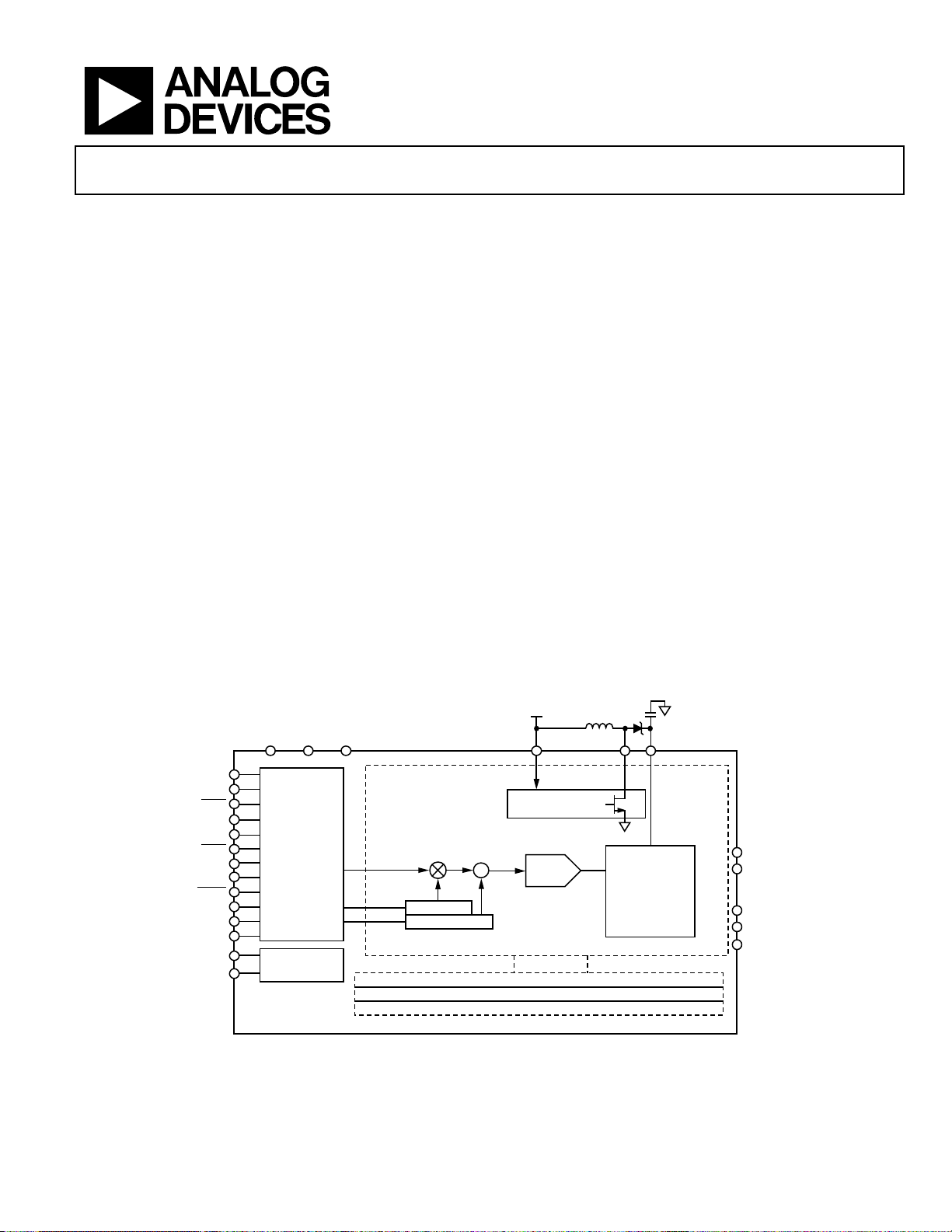
GENERAL DESCRIPTION
The AD5755 is a quad, voltage and current output DAC that
operates with a power supply range from −26.4 V to +33 V.
AD5755
On-chip dynamic power control minimizes package power
dissipation in current mode. This is achieved by regulating the
voltage on the output driver from 7.4 V to 29.5 V using a dc-todc boost converter optimized for minimum on chip power
dissipation.
The part uses a versatile 3-wire serial interface that operates at
clock rates of up to 30 MHz and is compatible with standard
SPI, QSPI™, MICROWIRE™, DSP, and microcontroller interface standards. The interface also features optional CRC-8
packet error checking, as well as a watchdog timer that
monitors activity on the interface.
PRODUCT HIGHLIGHTS
1. Dynamic power control for thermal management.
2. 16-bit performance.
3. Multichannel.
COMPANION PRODUCTS
Product Family: AD5755-1, AD5757
External References: ADR445, ADR02
Digital Isolators: ADuM1410, ADuM1411
Power: ADP2302, ADP2303
Additional companion products on the AD5755 product page
FUNCTIONAL BLOCK DIAGRAM
AV
SS
–15V AG ND
DV
DD
DGND
LDAC
SCLK
SDIN
SYNC
SDO
CLEAR
FAU LT
ALERT
AD1
AD0
REFOUT
REFIN
DIGITAL
INTERFACE
REFERENCE
AD5755
NOTES
1. x = A, B, C, AND D.
Rev. A
Information furnished by Analog Devices is believed to be accurate and reliable. However, no
responsibility is assumed by Anal og Devices for its use, nor for any infringements of patents or ot her
rights of third parties that may result from its use. Specifications subject to change without notice. No
license is granted by implication or otherwise under any patent or patent rights of Analog Devices.
Trademarks and registered trademarks are the property of their respective owners.
AV
+15V
DD
GAIN REG A
OFFSET REG A
DAC CHANNEL A
DAC CHANNEL B
DAC CHANNEL C
DAC CHANNEL D
V
CC
5.0V
SW
DC-TO-DC
CONVERTER
+
DAC A
V
x
CURRENT AND
OUTPUT RANGE
BOOST_x
7.4V TO 29.5V
VOLTAGE
SCALING
I
OUT_x
R
SET_x
+V
V
OUT_x
–V
SENSE_x
SENSE_x
07304-100
Figure 1.
One Technology Way, P.O. Box 9106, Norwood, MA 02062-9106, U.S.A.
Tel: 781.329.4700 www.analog.com
Fax: 781.461.3113 ©2011 Analog Devices, Inc. All rights reserved.

AD5755 Data Sheet
TABLE OF CONTENTS
Features.............................................................................................. 1
Applications....................................................................................... 1
General Description ......................................................................... 1
Product Highlights ........................................................................... 1
Companion Products....................................................................... 1
Functional Block Diagram .............................................................. 1
Revision History ............................................................................... 3
Detailed Functional Block Diagram .............................................. 4
Specifications..................................................................................... 5
AC Performance Characteristics ................................................ 8
Timing Characteristics ................................................................ 9
Absolute Maximum Ratings.......................................................... 12
ESD Caution................................................................................ 12
Pin Configuration and Function Descriptions........................... 13
Typical Performance Characteristics ........................................... 16
Voltage Outputs .......................................................................... 16
Current Outputs ......................................................................... 20
DC-to-DC Block......................................................................... 24
Reference ..................................................................................... 25
General......................................................................................... 26
Terminology .................................................................................... 27
Theory of Operation ...................................................................... 29
DAC Architecture....................................................................... 29
Power-On State of AD5755....................................................... 29
Serial Interface ............................................................................ 30
Transfer Function....................................................................... 30
Registers........................................................................................... 31
Programming Sequence to Write/Enable the Output
Correctly ...................................................................................... 32
Changing and Reprogramming the Range ............................. 32
Data Registers ............................................................................. 33
Control Registers........................................................................ 35
Readback Operation .................................................................. 38
Device Features............................................................................... 40
Output Fault................................................................................ 40
Voltage Output Short-Circuit Protection................................ 40
Digital Offset and Gain Control............................................... 40
Status Readback During a Write .............................................. 40
Asynchronous Clear................................................................... 41
Packet Error Checking............................................................... 41
Watchdog Timer......................................................................... 41
Output Alert................................................................................ 41
Internal Reference...................................................................... 41
External Current Setting Resistor ............................................ 41
Digital Slew Rate Control.......................................................... 42
Power Dissipation control......................................................... 42
DC-to-DC Converters............................................................... 42
AIcc Supply Requirements—Static............................................ 44
AICC Supply Requirements—Slewing ...................................... 44
Applications Information.............................................................. 46
Voltage and Current Output Ranges on the Same Terminal 46
Current Output Mode with Internal R
Precision Voltage Reference Selection..................................... 46
Driving Inductive Loads............................................................ 47
Transient Voltage Protection .................................................... 47
Microprocessor Interfacing....................................................... 47
Layout Guidelines....................................................................... 47
Galvanically Isolated Interface ................................................. 48
Outline Dimensions....................................................................... 49
Ordering Guide .......................................................................... 49
................................ 46
SET
Rev. A | Page 2 of 52

Data Sheet AD5755
REVISION HISTORY
11/11—Rev. 0 to Rev. A
Changes to Figure 2...........................................................................4
Changes to Table 1 ............................................................................5
Added Timing Diagram heading and changes to Figure 5........10
Changes to Figure 6.........................................................................11
Changes to Table 5 ..........................................................................13
Changes to Figure 13 ......................................................................16
Changes to Figure 21 ......................................................................18
Changes to Figure 37 ......................................................................20
Changes to Figure 44 ......................................................................22
Changes to Figure 56 and Figure 58 .............................................24
Changes to Figure 71 ......................................................................29
Changes to Power-On State of AD5575 Section.........................29
Changes to Table 17........................................................................35
Changes to Readback Operation Section and changes to
Table 26.............................................................................................38
Changes to Voltage Output Short-Circuit Protection Section..40
Changes to Figure 78 ......................................................................41
Changes to Figure 81 through Figure 84 Captions.....................44
Changes to Transient Voltage Protection Section and changes to
Figure 85...........................................................................................47
Changes to Galvanically Isolated Interface Section....................48
5/11—Revision 0: Initial Version
Rev. A | Page 3 of 52
AD5755 Data Sheet
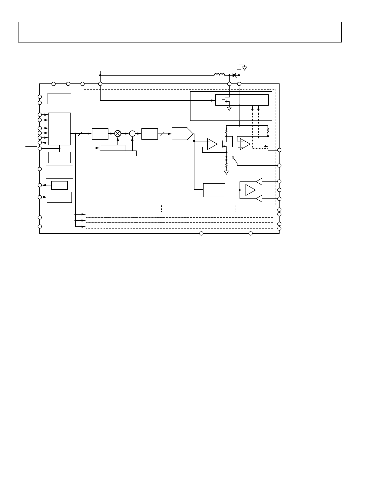
DETAILED FUNCTIONAL BLOCK DIAGRAM
AV
CC
5.0V
AV
SS
–15V AGND
AV
+15V
DD
SW
V
A
BOOST_A
DV
DGND
LDAC
CLEAR
SCLK
SDIN
SYNC
SDO
FAULT
ALERT
REFOUT
REFIN
AD1
AD0
DD
POWER-ON
RESET
INPUT
SHIFT
REGISTER
AND
CONTROL
STATUS
REGISTER
WATCHDOG
TIMER
(SPI ACTIVITY)
VREF
REFERENCE
BUFFERS
AD5755
16
INPUT
REG A
GAIN REG A
OFFSET REG A
DAC CHANNEL A
DAC CHANNEL B
DAC CHANNEL C
DAC CHANNEL D
DC-TO-DC
CONVERTER
V
POWER
CONTROL
16
DAC
+
REG A
DAC A
7.4V TO 29.5V
R2 R3
R1
VOUT
RANGE
SCALING
SWB, SWC, SW
V
D
SEN1VSEN2
REG
BOOST_B,VBOOST_C,VBOOST_D
I
OUT_A
R
SET_A
+V
V
OUT_A
–V
I
OUT_B
R
SET_B
+V
SENSE_B
V
OUT_B
SENSE_A
SENSE_A
, I
OUT_C
, R
,
V
SET_C
, +V
OUT_C
, I
OUT_D
, R
SENSE_
,
SET_D
V
OUT_D
, +V
C
SENSE_
D
07304-001
Figure 2.
Rev. A | Page 4 of 52

Data Sheet AD5755
SPECIFICATIONS
AVDD = V
GNDSW
otherwise noted.
Table 1.
Parameter1 Min Typ Max Unit Test Conditions/Comments
VOLTAGE OUTPUT
Output Voltage Ranges 0 5 V
0 10 V
−5 +5 V
−10 +10 V
0 6 V
0 12 V
−6 +6 V
−12 +12 V
Resolution 16 Bits
ACCURACY AVSS = −15 V, loaded and unloaded
Total Unadjusted Error (TUE)
B Version −0.04 +0.04 % FSR
−0.03 ±0.0032 +0.03 % FSR TA = 25°C
A Version −0.25 +0.25 % FSR
−0.075 ±0.02 +0.075 % FSR TA = 25°C
TUE Long-Term Stability 35 ppm FSR Drift after 1000 hours, TJ = 150°C
Relative Accuracy (INL) −0.006 ±0.0012 +0.006 % FSR 0 V to 5 V, 0 V to 10 V, ±5 V, ±10 V ranges
−0.008 ±0.0012 +0.008 % FSR On overranges
Differential Nonlinearity (DNL) −1 +1 LSB Guaranteed monotonic
Zero-Scale Error −0.03 ±0.002 +0.03 % FSR
Zero-Scale TC2 ±2
Bipolar Zero Error −0.03 ±0.002 +0.03 % FSR
Bipolar Zero TC
Offset Error −0.03 ±0.002 +0.03 % FSR
Offset TC2 ±2
Gain Error −0.03 ±0.004 +0.03 % FSR
Gain TC2 ±3
Full-Scale Error −0.03 ±0.002 +0.03 % FSR
Full-Scale TC2 ±2
OUTPUT CHARACTERISTICS2
Headroom 1 2.2 V With respect to V
Footroom 1 1.4 V With respect to the AVSS supply
Output Voltage Drift vs. Time 20 ppm FSR
Short-Circuit Current 12/6 16/8 mA
Load 1 kΩ For specified performance
Capacitive Load Stability 10 nF
2 μF
DC Output Impedance 0.06 Ω
DC PSRR 50 μV/V
= 15 V; AVSS = −15 V; DVDD = 2.7 V to 5.5 V; AVCC = 4.5 V to 5.5 V; dc-to-dc converter disabled; AGND = DGND =
BOOST_x
= 0 V; REFIN = 5 V; voltage outputs: RL = 1 kΩ, CL = 220 pF; current outputs: RL = 300 Ω; all specifications T
x
ppm
FSR/°C
2
±1
ppm
FSR/°C
ppm
FSR/°C
ppm
FSR/°C
ppm
FSR/°C
supply
BOOST
Drift after 1000 hours, ¾ scale output, T
= −15 V
AV
SS
Programmable by user, defaults to 16 mA typical
level
External compensation capacitor of 220 pF
connected
Rev. A | Page 5 of 52
MIN
to T
, unless
MAX
= 150°C,
J

AD5755 Data Sheet
Parameter1 Min Typ Max Unit Test Conditions/Comments
DC Crosstalk 24 μV
CURRENT OUTPUT
Output Current Ranges 0 24 mA
0 20 mA
4 20 mA
Resolution 16 Bits
ACCURACY (EXTERNAL R
Total Unadjusted Error (TUE)
B Version −0.05 ±0.009 +0.05 % FSR
A Version −0.2 ±0.04 +0.2 % FSR
TUE Long-Term Stability 100 ppm FSR Drift after 1000 hours, TJ = 150°C
Relative Accuracy (INL) −0.006 +0.006 % FSR
Differential Nonlinearity (DNL) −1 +1 LSB Guaranteed monotonic
Offset Error −0.05 ±0.005 +0.05 % FSR
Offset Error Drift2 ±4
Gain Error −0.05 ±0.004 +0.05 % FSR
Gain TC2 ±3
Full-Scale Error −0.05 ±0.008 +0.05 % FSR
Full-Scale TC2 ±5
DC Crosstalk 0.0005 % FSR External R
ACCURACY (INTERNAL R
Total Unadjusted Error (TUE)
B Version −0.14 +0.14 % FSR
−0.11 ±0.009 +0.11 % FSR TA = 25°C
A Version −0.35 +0.35 % FSR
−0.2 +0.04 +0.2 % FSR TA = 25°C
TUE Long-Term Stability 180 ppm FSR Drift after 1000 hours, TJ = 150°C
Relative Accuracy (INL) −0.006 +0.006 % FSR
Relative Accuracy (INL) −0.004 +0.004 % FSR TA = 25°C
Differential Nonlinearity (DNL) −1 +1 LSB Guaranteed monotonic
Offset Error
3, 4
−0.05 +0.05 % FSR
−0.04 ±0.007 +0.04 % FSR TA = 25°C
Offset Error Drift2 ±6
Gain Error −0.12 +0.12 % FSR
−0.06 ±0.002 +0.06 % FSR TA = 25°C
Gain TC2 ±9
Full-Scale Error
3, 4
−0.1 ±0.007 +0.1 % FSR TA = 25°C
Full-Scale TC2 ±14
DC Crosstalk4 −0.011 % FSR Internal R
OUTPUT CHARACTERISTICS2
Current Loop Compliance Voltage
Output Current Drift vs. Time Drift after 1000 hours, ¾ scale output, TJ = 150°C
90 ppm FSR External R
140 ppm FSR Internal R
)
SET
Assumes ideal resistor; see the External Current
Setting Resistor section for more information.
ppm
FSR/°C
ppm
FSR/°C
ppm
FSR/°C
SET
)
SET
3, 4
ppm
FSR/°C
ppm
FSR/°C
−0.14 +0.14 % FSR
ppm
FSR/°C
SET
V
BOOST_x
− 2.4
V
BOOST_x
2.7
V
−
SET
SET
Rev. A | Page 6 of 52

Data Sheet AD5755
Parameter1 Min Typ Max Unit Test Conditions/Comments
Resistive Load 1000 Ω
Output Impedance 100 MΩ
DC PSRR 0.02 1 μA/V
REFERENCE INPUT/OUTPUT
Reference Input2
Reference Input Voltage 4.95 5 5.05 V For specified performance
DC Input Impedance 45 150 MΩ
Reference Output
Output Voltage 4.995 5 5.005 V TA = 25°C
Reference TC2 −10 ±5 +10 ppm/°C
Output Noise (0.1 Hz to 10 Hz)2 7 μV p-p
Noise Spectral Density2 100 nV/√Hz At 10 kHz
Output Voltage Drift vs. Time2 180 ppm Drift after 1000 hours, TJ = 150°C
Capacitive Load2 1000 nF
Load Current 9 mA See Figure 63
Short-Circuit Current 10 mA
Line Regulation2 3 ppm/V See Figure 64
Load Regulation2 95 ppm/mA See Figure 63
Thermal Hysteresis2 160 ppm First temperature cycle
5 ppm Second temperature cycle
DC-TO-DC
Switch
Switch On Resistance 0.425 Ω
Switch Leakage Current 10 nA
Peak Current Limit 0.8 A
Oscillator
Oscillator Frequency 11.5 13 14.5 MHz
Maximum Duty Cycle 89.6 % At 410 kHz dc-to-dc switching frequency
DIGITAL INPUTS2 JEDEC compliant
VIH, Input High Voltage 2 V
VIL, Input Low Voltage 0.8 V
Input Current −1 +1 μA Per pin
Pin Capacitance 2.6 pF Per pin
DIGITAL OUTPUTS2
SDO, ALERT
VOL, Output Low Voltage 0.4 V Sinking 200 μA
VOH, Output High Voltage
High Impedance Leakage
Current
High Impedance Output
Capacitance
FAU LT
VOL, Output Low Voltage 0.4 V 10 kΩ pull-up resistor to DVDD
VOL, Output Low Voltage 0.6 V At 2.5 mA
VOH, Output High Voltage 3.6 V 10 kΩ pull-up resistor to DVDD
POWER REQUIREMENTS
AVDD 9 33 V
AVSS −26.4 −10.8 V
DVDD 2.7 5.5 V
DVDD −
0.5
−1 +1 μA
2.5 pF
V Sourcing 200 μA
The dc-to-dc converter has been characterized
with a maximum load of 1 kΩ, chosen such that
compliance is not exceeded; see Figure 52 and
DC-DC MaxV bits in Table 25
This oscillator is divided down to give the dc-to-dc
converter switching frequency
Rev. A | Page 7 of 52

AD5755 Data Sheet
Parameter1 Min Typ Max Unit Test Conditions/Comments
AVCC 4.5 5.5 V
AIDD 8.6 10.5 mA
7 7.5 mA Current output mode on all channels,
AISS −11 −8.8 mA
−1.7 mA Current output mode on all channels
DICC 9.2 11 mA
AICC 1 mA Output unloaded, over supplies
5
I
2.7 mA
BOOST
1 mA Per channel, current output mode
Power Dissipation 173 mW
1
Temperature range: −40°C to +105°C; typical at +25°C.
2
Guaranteed by design and characterization; not production tested.
3
For current outputs with internal R
loaded with the same code.
4
See the Current Output Mode with Internal R
5
Efficiency plots in Figure 54, Figure 55, Figure 56, and Figure 57 include the I
, the offset, full-scale, and TUE measurements exclude dc crosstalk. The measurements are made with all four channels enabled
SET
section for more explanation of the dc crosstalk.
SET
quiescent current.
BOOST
AC PERFORMANCE CHARACTERISTICS
AVDD = V
GNDSW
otherwise noted.
= 15 V; AVSS = −15 V; DVDD = 2.7 V to 5.5 V; AVCC = 4.5 V to 5.5 V; dc-to-dc converter disabled; AGND = DGND =
BOOST_x
= 0 V; REFIN = 5 V; voltage outputs: RL = 2 kΩ, CL = 220 pF; current outputs: RL = 300 Ω; all specifications T
x
Voltage output mode on all channels, output
unloaded, over supplies
Voltage output mode on all channels, output
unloaded, over supplies
= DVDD, VIL = DGND, internal oscillator running,
V
IH
over supplies
Per channel, voltage output mode, output
unloaded, over supplies
= 15 V, AVSS = −15 V, dc-to-dc converter
AV
DD
enable, current output mode, outputs disabled
MIN
to T
MAX
, unless
Table 2.
Parameter1 Min Typ Max Unit Test Conditions/Comments
DYNAMIC PERFORMANCE
Voltage Output
Output Voltage Settling Time 11 μs 5 V step to ±0.03% FSR, 0 V to 5 V range
18 μs 10 V step to ±0.03% FSR, 0 V to 10 V range
13 μs
100 mV step to 1 LSB (16-bit LSB), 0 V to 10 V
range
Slew Rate 1.9 V/μs 0 V to 10 V range
Power-On Glitch Energy 150 nV-sec
Digital-to-Analog Glitch Energy 6 nV-sec
Glitch Impulse Peak Amplitude 25 mV
Digital Feedthrough 1 nV-sec
DAC to DAC Crosstalk 2 nV-sec 0 V to 10 V range
Output Noise (0.1 Hz to 10 Hz
0.15 LSB p-p 16-bit LSB, 0 V to 10 V range
Bandwidth)
Output Noise Spectral Density 150 nV/√Hz
Measured at 10 kHz, midscale output, 0 V to 10 V
range
AC PSRR 83 dB
200 mV 50 Hz/60 Hz sine wave superimposed on
power supply voltage
Current Output
Output Current Settling Time 15 μs To 0.1% FSR (0 mA to 24 mA)
See test conditions/
ms See Figure 48, Figure 49, and Figure 50
comments
Output Noise (0.1 Hz to 10 Hz
0.15 LSB p-p 16-bit LSB, 0 mA to 24 mA range
Bandwidth)
Output Noise Spectral Density 0.5 nA/√Hz
Measured at 10 kHz, midscale output, 0 mA to
24 mA range
1
Guaranteed by design and characterization; not production tested.
Rev. A | Page 8 of 52
Data Sheet AD5755
TIMING CHARACTERISTICS
AVDD = V
GNDSW
otherwise noted.
= 15 V; AVSS = −15 V; DVDD = 2.7 V to 5.5 V; AVCC = 4.5 V to 5.5 V; dc-to-dc converter disabled; AGND = DGND =
BOOST_x
= 0 V; REFIN = 5 V; voltage outputs: RL = 1 kΩ, CL = 220 pF; current outputs: RL = 300 Ω; all specifications T
x
MIN
to T
MAX
, unless
Table 3.
Parameter
1, 2, 3
Limit at T
MIN
, T
Unit Description
MAX
t1 33 ns min SCLK cycle time
t2 13 ns min SCLK high time
t3 13 ns min SCLK low time
t4 13 ns min
t5 13 ns min
t6 198 ns min
falling edge to SCLK falling edge setup time
SYNC
th
/32nd SCLK falling edge to SYNC rising edge (see ) Figure 77
24
high time
SYNC
t7 5 ns min Data setup time
t8 5 ns min Data hold time
t9 20 μs min
rising edge to LDAC falling edge (all DACs updated or any channel has
SYNC
digital slew rate control enabled)
5 μs min
t10 10 ns min
t11 500 ns max
t12
See the AC Performance
μs max DAC output settling time
rising edge to LDAC falling edge (single DAC updated)
SYNC
pulse width low
LDAC
falling edge to DAC output response time
LDAC
Characteristics section
t13 10 ns min CLEAR high time
t14 5 μs max CLEAR activation time
t15 40 ns max SCLK rising edge to SDO valid
t16 21 μs min
5 μs min
t17 500 ns min
t18 800 ns min
4
t
20 μs min
19
5 μs min
rising edge to DAC output response time (LDAC = 0) (all DACs updated)
SYNC
rising edge to DAC output response time (LDAC = 0) (single DAC updated)
SYNC
falling edge to SYNC rising edge
LDAC
pulse width
RESET
high to next SYNC low (digital slew rate control enabled) (all DACs updated)
SYNC
high to next SYNC low (digital slew rate control disabled) (single DAC
SYNC
updated)
1
Guaranteed by design and characterization; not production tested.
2
All input signals are specified with t
3
See Figure 3, Figure 4, Figure 5, and Figure 6.
4
This specification applies if
LDAC
= t
= 5 ns (10% to 90% of DVDD) and timed from a voltage level of 1.2 V.
RISE
FALL
is held low during the write cycle; otherwise, see t9.
Rev. A | Page 9 of 52
AD5755 Data Sheet
Timing Diagrams
t
1
SCLK
SYNC
SDIN
LDAC
V
OUT_x
LDAC = 0
V
OUT_x
CLEAR
V
OUT_x
12 24
t
6
t
4
t
7
MSB
t
13
t
t
3
t
8
14
t
2
t
10
t
5
t
19
LSB
t
t
9
t
17
t
16
10
t
t
11
t
12
12
t
RESET
18
07304-002
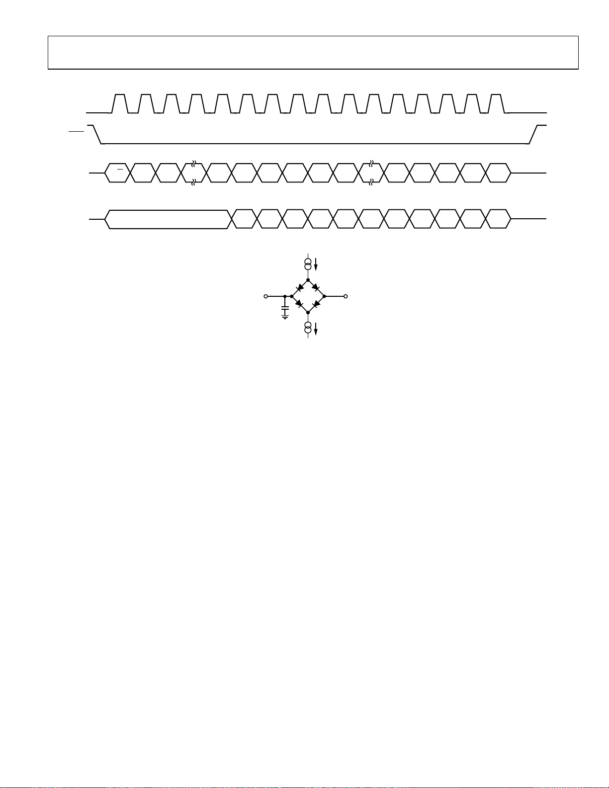
Figure 3. Serial Interface Timing Diagram
SCLK
SYNC
SDIN
SDO
1 1
MSB MSBLSB LSB
INPUT WORD SPECIFIES
REGISTER TO BE READ
UNDEFINED SELECTED REGISTER DATA
24 24
t
6
NOP CONDIT ION
MSB LSB
t
15
CLOCKED OUT
Figure 4. Readback Timing Diagram
07304-203
Rev. A | Page 10 of 52
Data Sheet AD5755
SCLK
SYNC
SDIN
SDO
LSB MSB
12 16
DUT_
R/W
DUT_
AD1
SDO DISABLED
XXXD15D14 D1D0
AD0
SDO_
ENAB
STATUSSTATUSSTATUSSTATUS
07304-204
Figure 5. Status Readback During Write
TO OUTPUT
PIN
50pF
C
200µA I
L
200µA I
OL
OH
VOH (MIN) OR
(MAX)
V
OL
07304-005
Figure 6. Load Circuit for SDO Timing Diagram
Rev. A | Page 11 of 52
AD5755 Data Sheet
ABSOLUTE MAXIMUM RATINGS
TA = 25°C, unless otherwise noted. Transient currents of up to
100 mA do not cause SCR latch-up.
Table 4.
Parameter Rating
AVDD, V
to AGND, DGND −0.3 V to +33 V
BOOST_x
AVSS to AGND, DGND +0.3 V to −28 V
AVDD to AVSS −0.3 V to +60 V
AVCC to AGND −0.3 V to +7 V
DVDD to DGND −0.3 V to +7 V
Digital Inputs to DGND
−0.3 V to DV
+ 0.3 V or +7 V
DD
(whichever is less)
Digital Outputs to DGND
−0.3 V to DV
+ 0.3 V or +7 V
DD
(whichever is less)
REFIN, REFOUT to AGND
−0.3 V to AV
+ 0.3 V or +7 V
DD
(whichever is less)
V
OUT_x
to AGND
AV
SS
to V
or 33 V if using
BOOST_x
the dc-to-dc circuitry
+V
SENSE_x
, −V
SENSE_x
to AGND
AV
SS
to V
or 33 V if using
BOOST_x
the dc-to-dc circuitry
I
OUT_x
to AGND
AV
SS
to V
or 33 V if using
BOOST_x
the dc-to-dc circuitry
SWx to AGND −0.3 to +33 V
AGND, GNDSWx to DGND −0.3 V to +0.3 V
Operating Temperature Range ( TA)
Industrial1 −40°C to +105°C
Storage Temperature Range −65°C to +150°C
Junction Temperature (TJ max) 125°C
64-Lead LFCSP
θJA Thermal Impedance2 20°C/W
Power Dissipation (TJ max − TA)/θJA
Lead Temperature JEDEC industry standard
Soldering J-STD-020
1
Power dissipated on chip must be derated to keep the junction temperature
below 125°C.
2
Based on a JEDEC 4-layer test board.
Stresses above those listed under Absolute Maximum Ratings
may cause permanent damage to the device. This is a stress
rating only; functional operation of the device at these or any
other conditions above those indicated in the operational
section of this specification is not implied. Exposure to absolute
maximum rating conditions for extended periods may affect
device reliability.
ESD CAUTION
Rev. A | Page 12 of 52
Data Sheet AD5755
PIN CONFIGURATION AND FUNCTION DESCRIPTIONS
LV_D
PIN 1
INDICATO R
DCDC_D
SENSE_D
SET_CRSET_D
R
646362616059585756555453525150
SENSE_D
REFOUT
REFIN
COMP
–V
+V
COMP
V
BOOST_DVOUT_D
LV_C
SENSE_C
SENSE_C
AVSSCOMP
OUT_C
–V
+V
V
49
OUT_D
I
R
1
SET_B
2
R
SET_A
REFGND
REFGND
NOTES
1. THIS EXPOSED PADDLE SHOULD BE CO NNECTED TO THE PO TENTIALOF T HE
AV
IT IS RE COMMENDED T HAT THE P ADDLE BE THERMALLY CO NNECTED TO A
COPPER PLANE FOR ENHANCED THERMAL PE RFORMANCE.
3
4
5
AD0
6
AD1
7
SYNC
8
SCLK
9
SDIN
10
SDO
DV
11
DD
12
DGND
13
LDAC
14
CLEAR
15
ALERT
16
FAULT
171819202122232425262728293031
POC
PIN, OR, ALTERNAT IVELY, IT CAN BE LEFT ELECTRI CALLY UNCO NNECTED.
SS
AV
RESET
DD
LV_A
–V
COMP
AD5755
TOP VIEW
(Not to Scale)
OUT_AIOUT_A
DCDC_A
V
SENSE_A+VSENSE_A
BOOST_A
V
COMP
AV
SS
32
LV_B
OUT_B
DCDC_B
V
SENSE_B+VSENSE_B
–V
COMP
COMP
48
47
46
45
44
43
42
41
40
39
38
37
36
35
34
33
COMP
I
OUT_C
V
BOOST_C
AV
CC
SW
C
GNDSW
GNDSW
SW
D
AV
SS
SW
A
GNDSW
GNDSW
SW
B
AGND
V
BOOST_B
I
OUT_B
DCDC_C
C
D
A
B
07304-006
Figure 7. Pin Configuration
Table 5. Pin Function Descriptions
Pin No. Mnemonic Description
1 R
SET_B
An external, precision, low drift 15 kΩ current setting resistor can be connected to this pin to improve the I
temperature drift performance. See the Device Features section.
2 R
SET_A
An external, precision, low drift 15 kΩ current setting resistor can be connected to this pin to improve the I
temperature drift performance. See the Device Features section.
3 REFGND Ground Reference Point for Internal Reference.
4 REFGND Ground Reference Point for Internal Reference.
5 AD0 Address Decode for the Device Under Test (DUT) on the Board.
6 AD1 Address Decode for the DUT on the Board.
7
Active Low Input. This is the frame synchronization signal for the serial interface. While SYNC is low, data is
SYNC
transferred in on the falling edge of SCLK.
8 SCLK
Serial Clock Input. Data is clocked into the input shift register on the falling edge of SCLK. This operates at clock
speeds of up to 30 MHz.
9 SDIN Serial Data Input. Data must be valid on the falling edge of SCLK.
10 SDO Serial Data Output. Used to clock data from the serial register in readback mode. See Figure 4 and Figure 5.
11 DVDD Digital Supply. The voltage range is from 2.7 V to 5.5 V.
12 DGND Digital Ground.
13
Load DAC, Active Low Input. This is used to update the DAC register and consequently the DAC outputs. When
LDAC
tied permanently low, the addressed DAC data register is updated on the rising edge of SYNC. If LDAC is held
high during the write cycle, the DAC input register is updated, but the DAC output update only takes place at
14 CLEAR
the falling edge of LDAC
LDAC
pin must not be left unconnected.
Active High, Edge Sensitive Input. Asserting this pin sets the output current and voltage to the preprogrammed
(see ). Using this mode, all analog outputs can be updated simultaneously. The Figure 3
clear code bit setting. Only channels enabled to be cleared are cleared. See the Device Features section for more
information. When CLEAR is active, the DAC output register cannot be written to.
OUT_B
OUT_A
Rev. A | Page 13 of 52

AD5755 Data Sheet
Pin No. Mnemonic Description
15 ALERT
16
FAU LT
17 POC
18
RESET
19 AVDD Positive Analog Supply. The voltage range is from 9 V to 33 V.
20 COMP
21 −V
22 +V
23 COMP
24 V
25 V
26 I
LV_A
SENSE_A
SENSE_A
DCDC_A
BOOST_A
Buffered Analog Output Voltage for DAC Channel A.
OUT_A
Current Output Pin for DAC Channel A.
OUT_A
27 AVSS Negative Analog Supply Pin. Voltage range is from −10.8 V to −26.4 V.
28 COMP
29 −V
30 +V
31 V
32 COMP
33 I
34 V
LV_B
SENSE_B
SENSE_B
Buffered Analog Output Voltage for DAC Channel B.
OUT_B
DCDC_B
Current Output Pin for DAC Channel B.
OUT_B
BOOST_B
35 AGND Ground Reference Point for Analog Circuitry. This must be connected to 0 V.
36 SWB
37 GNDSWB Ground Connection for DC-to-DC Switching Circuit. This pin should always be connected to ground.
38 GNDSWA Ground Connection for DC-to-DC Switching Circuit. This pin should always be connected to ground.
39 SWA
40 AVSS Negative Analog Supply Pin. The voltage range is from −10.8 V to −26.4 V.
41 SWD
42 GNDSWD Ground Connections for DC-to-DC Switching Circuit. This pin should always be connected to ground.
43 GNDSWC Ground Connections for DC-to-DC Switching Circuit. This pin should always be connected to ground.
Active High Output. This pin is asserted when there has been no SPI activity on the interface pins for a
predetermined time. See the Device Features section for more information.
Active Low Output. This pin is asserted low when an open circuit in current mode is detected, a short circuit in
voltage mode is detected, a PEC error is detected, or an overtemperature is detected (see the Device Features
section). Open-drain output.
Power-On Condition. This pin determines the power-on condition and is read during power-on or, alternatively,
after a device reset. If POC = 0, the device is powered up with the voltage and current channels in tristate mode.
If POC = 1, the device is powered up with a 30 kΩ pull-down resistor to ground on the voltage output channel,
and the current channel is in tristate mode.
Hardware Reset, Active Low Input.
Optional Compensation Capacitor Connection for V
this pin and the V
pin allows the voltage output to drive up to 2 μF. Note that the addition of this capacitor
OUT_A
Output Buffer. Connecting a 220 pF capacitor between
OUT_A
reduces the bandwidth of the output amplifier, increasing the settling time.
Sense Connection for the Negative Voltage Output Load Connection for V
. This pin must stay within ±3.0 V
OUT_A
of AGND for specified operation.
Sense Connection for the Positive Voltage Output Load Connection for V
DC-to-DC Compensation Capacitor. Connect a 10 nF capacitor from this pin to ground. Used to regulate the
OUT_A
.
feedback loop of the Channel A dc-to-dc converter. Alternatively, if using an external compensation resistor,
place a resistor in series with a capacitor to ground from this pin (see the DC-to-DC Converter Compensation
Capacitors and the AICC Supply Requirements—Slewing sections in the Device Features section for more
information).
Supply for Channel A Current Output Stage (see Figure 72). This is also the supply for the V
stage, which is
OUT_x
regulated to 15 V by the dc-to-dc converter. To use the dc-to-dc feature of the device, connect as shown in
Figure 78.
Optional Compensation Capacitor Connection for V
this pin and the V
pin allows the voltage output to drive up to 2 μF. Note that the addition of this capacitor
OUT_B
Output Buffer. Connecting a 220 pF capacitor between
OUT_B
reduces the bandwidth of the output amplifier, increasing the settling time.
Sense Connection for the Negative Voltage Output Load Connection for V
. This pin must stay within ±3.0 V
OUT_B
of AGND for specified operation.
Sense Connection for the Positive Voltage Output Load Connection for V
DC-to-DC Compensation Capacitor. Connect a 10 nF capacitor from this pin to ground. Used to regulate the
OUT_B
.
feedback loop of the Channel B dc-to-dc converter. Alternatively, if using an external compensation resistor,
place a resistor in series with a capacitor to ground from this pin (see the DC-to-DC Converter Compensation
Capacitors and the AICC Supply Requirements—Slewing sections in the Device Features section for more
information).
Supply for Channel B Current Output Stage (see Figure 72). This is also the supply for the V
stage, which is
OUT_x
regulated to 15 V by the dc-to-dc converter. To use the dc-to-dc feature of the device, connect as shown in
Figure 78.
Switching Output for Channel B DC-to-DC Circuitry. To use the dc-to-dc feature of the device, connect as shown
in Figure 78.
Switching Output for Channel A DC-to-DC Circuitry. To use the dc-to-dc feature of the device, connect as shown
in Figure 78.
Switching Output for Channel D DC-to-DC Circuitry. To use the dc-to-dc feature of the device, connect as shown
in Figure 78.
Rev. A | Page 14 of 52

Data Sheet AD5755
Pin No. Mnemonic Description
44 SWC
45 AVCC Supply for DC-to-DC Circuitry.
46 V
47 I
48 COMP
49 V
50 +V
51 −V
52 COMP
BOOST_C
Current Output Pin for DAC Channel C.
OUT_C
DCDC_C
Buffered Analog Output Voltage for DAC Channel C.
OUT_C
SENSE_C
SENSE_C
LV_C
53 AVSS Negative Analog Supply Pin.
54 I
55 V
56 V
57 COMP
58 +V
59 −V
60 COMP
Current Output Pin for DAC Channel D.
OUT_D
Buffered Analog Output Voltage for DAC Channel D.
OUT_D
BOOST_D
DCDC_D
SENSE_D
SENSE_D
LV_D
61 REFIN External Reference Voltage Input.
62 REFOUT
63 R
64 R
SET_D
SET_C
EPAD
Switching Output for Channel C DC-to-DC Circuitry. To use the dc-to-dc feature of the device, connect as shown
in Figure 78.
Supply for Channel C Current Output Stage (see Figure 72). This is also the supply for the V
stage, which is
OUT_x
regulated to 15 V by the dc-to-dc converter. To use the dc-to-dc feature of the device, connect as shown in
Figure 78.
DC-to-DC Compensation Capacitor. Connect a 10 nF capacitor from this pin to ground. Used to regulate the
feedback loop of the Channel C dc-to-dc converter. Alternatively, if using an external compensation resistor,
place a resistor in series with a capacitor to ground from this pin (see the DC-to-DC Converter Compensation
Capacitors and AICC Supply Requirements—Slewing sections in the Device Features section for more
information).
Sense Connection for the Positive Voltage Output Load Connection for V
Sense Connection for the Negative Voltage Output Load Connection for V
.
OUT_C
. This pin must stay within ±3.0 V
OUT_C
of AGND for specified operation.
Optional Compensation Capacitor Connection for V
this pin and the V
pin allows the voltage output to drive up to 2 μF. Note that the addition of this capacitor
OUT_C
Output Buffer. Connecting a 220 pF capacitor between
OUT_C
reduces the bandwidth of the output amplifier, increasing the settling time.
Supply for Channel D Current Output Stage (see Figure 72). This is also the supply for the V
OUT_x
regulated to 15 V by the dc-to-dc converter. To use the dc-to-dc feature of the device, connect as shown in
Figure 78.
DC-to-DC Compensation Capacitor. Connect a 10 nF capacitor from this pin to ground. Used to regulate the
feedback loop of Channel D dc-to-dc converter. Alternatively, if using an external compensation resistor, place a
resistor in series with a capacitor to ground from this pin (see the DC-to-DC Converter Compensation Capacitors
and AICC Supply Requirements—Slewing sections in the Device Features section for more information).
Sense Connection for the Positive Voltage Output Load Connection for V
Sense Connection for the Negative Voltage Output Load Connection for V
.
OUT_D
. This pin must stay within ±3.0 V
OUT_D
of AGND for specified operation.
Optional Compensation Capacitor Connection for V
this pin and the V
pin allows the voltage output to drive up to 2 μF. Note that the addition of this capacitor
OUT_D
Output Buffer. Connecting a 220 pF capacitor between
OUT_D
reduces the bandwidth of the output amplifier, increasing the settling time.
Internal Reference Voltage Output. It is recommended to place a 0.1 μF capacitor between REFOUT and
REFGND.
An external, precision, low drift 15 kΩ current setting resistor can be connected to this pin to improve the I
temperature drift performance. See the Device Features section.
An external, precision, low drift 15 kΩ current setting resistor can be connected to this pin to improve the I
temperature drift performance. See the Device Features section.
Exposed Pad. This exposed pad should be connected to the potential of the AV
pin, or, alternatively, it can be
SS
left electrically unconnected. It is recommended that the pad be thermally connected to a copper plane for
enhanced thermal performance.
stage, which is
OUT_D
OUT_C
Rev. A | Page 15 of 52
AD5755 Data Sheet
TYPICAL PERFORMANCE CHARACTERISTICS
VOLTAGE OUTPUTS
0.0015
0.0010
0.0005
INL ERRO R (%FSR)
–0.0005
±10V RANGE
±5V RANGE
+10V RANGE
+5V RANGE
+10V RANGE W ITH DCDC
0
AVDD = +15V
AVSS = –15V
= 25°C
T
A
0.0015
0.0010
0.0005
INL (%FSR)
–0.0005
–0.0010
+5V RANGE MAX INL +10V RANG E MAX INL
±5V RANGE MAX INL ±10V RANGE MAX IN L
+5V RANGE MIN INL + 10V RANGE MIN INL
±5V RANGE MIN INL ±10V RANGE M IN INL
0
AV
= +15V
DD
AV
= –15V
SS
OUTPUT UNLOADED
–0.0010
0 10k 20k 30k 40k 50k 60k
CODE
Figure 8. Integral Nonlinearity Error vs. DAC Code
1.0
0.8
0.6
0.4
0.2
–0.2
DNL ERROR (LSB)
–0.4
–0.6
–0.8
–1.0
±10V RANGE
±5V RANGE
+10V RANGE
+5V RANGE
+10V RANGE W ITH DCDC
0
0 10k 20k 30k 40k 50k 60k
CODE
AVDD = +15V
= –15V
AV
SS
= 25°C
T
A
Figure 9. Differential Nonlinearity Error vs. DAC Code
–0.002
–0.004
–0.006
TOTAL UNADJUSTED ERROR (%F SR)
–0.008
–0.010
0.006
0.004
0.002
0
0
10k 20k 30k 40k 50k 60k
±10V RANGE
±5V RANGE
+10V RANGE
+5V RANGE
+10V RANGE WITH DCDC
CODE
Figure 10. Total Unadjusted Error vs. DAC Code
AVDD = +15V
= –15V
AV
SS
= 25°C
T
A
–0.0015
–40 –20 0 20 40 60 80 100
07304-023
TEMPERATURE (°C)
07304-127
Figure 11. Integral Nonlinearity Error vs. Temperature
1.0
0.8
0.6
0.4
0.2
–0.2
DNL ERROR (LSB)
–0.4
–0.6
–0.8
–1.0
07304-024
AVDD = +15V
= –15V
AV
SS
ALL RANGES
0
–40 –20 0 20 40 60 80 100
DNL ERROR MAX
DNL ERROR MIN
TEMPERATURE (°C)
07304-128
Figure 12. Differential Nonlinearity Error vs. Temperature
0.012
0.010
0.008
0.006
0.004
0.002
0
–0.002
TOTAL UNADJUSTED ERROR (%F SR)
–0.004
–0.006
–40 –20 0 20 40 60 80 100
07304-025
+5V RANGE
+10V RANGE
±5V RANGE
±10V RANGE
AVDD = +15V
AV
= –15V
SS
OUTPUT UNLOADED
TEMPERATURE (°C)
07304-129
Figure 13. Total Unadjusted Error vs. Temperature
Rev. A | Page 16 of 52

Data Sheet AD5755
0.012
0.010
0.008
0.006
0.004
0.002
0
–0.002
FULL-S CALE ERROR (%FSR)
–0.004
–0.006
–40 –20 0 20 40 60 80 100
+5V RANGE
+10V RANGE
±5V RANGE
±10V RANGE
AVDD = +15V
AV
= –15V
SS
OUTPUT UNLOADED
TEMPERATURE (° C)
Figure 14. Full-Scale Error vs. Temperature
0.0015
0.0010
0.0005
0
–0.0005
–0.0010
OFFSET (%FSR)
–0.0015
–0.0020
–0.0025
–40 –20 0 20 40 60 80 100
+5V RANGE
+10V RANGE
AVDD = +15V
AV
= –15V
SS
OUTPUT UNLOADED
TEMPERATURE (°C)
Figure 15. Offset Error vs. Temperature
07304-132
07304-133
0.010
0.008
0.006
0.004
0.002
0
GAIN ERROR (%FSR)
–0.002
–0.004
–0.006
–40 –20 0 20 40 60 80 100
+5V RANGE
+10V RANGE
±5V RANGE
±10V RANGE
AVDD = +15V
AV
= –15V
SS
OUTPUT UNLOADED
TEMPERATURE (°C)
Figure 17. Gain Error vs. Temperature
0.0015
0.0010
0.0005
0
–0.0005
+5V RANGE
–0.0010
ZERO-SCALE ERROR (%FSR)
–0.0015
–0.0020
+10V RANGE
±5V RANGE
±10V RANGE
AVDD = +15V
AV
= –15V
SS
OUTPUT UNL OADED
–40 –20 0 20 40 60 80 100
TEMPERATURE (°C)
Figure 18. Zero-Scale Error vs. Temperature
07304-135
07304-136
0.0025
0.0020
0.0015
0.0010
0.0005
0
–0.0005
–0.0010
BIPOLAR ZERO ERROR (%FSR)
–0.0015
–0.0020
–40 –20 0 20 40 60 80 100
±5V RANGE
±10V RANGE
AVDD = +15V
AV
= –15V
SS
OUTPUT UNLOADE D
TEMPERATURE (°C)
Figure 16. Bipolar Zero Error vs. Temperature
07304-134
Rev. A | Page 17 of 52
0.0020
0.0015
0.0010
0.0005
–0.0005
INL EROR (%FSR)
–0.0010
–0.0015
–0.0020
0V TO 10V RANG E MAX INL
0V TO 10V RANG E MIN INL
0
T
= 25°C
A
AV
= –26.4V FO R AVDD > +26.4V
SS
10 15 20 25 30
SUPPLY (V)
Figure 19. Integral Nonlinearity Error vs. AV
/|AVSS|
DD
07304-034

AD5755 Data Sheet
1.0
AV
= +15V
DD
= –15V
AV
0.8
SS
ALL RANGES
0.6
T
= 25°C
A
AVSS = –26.4V FOR AVDD > +26.4V
0.4
0.2
DNL ERROR MAX
0
DNL ERROR MI N
–0.2
DNL ERROR (LSB)
–0.4
–0.6
–0.8
–1.0
10 15 20 25 30
SUPPLY (V)
Figure 20. Differential Nonlinearity Error vs. AV
DD
/|AVSS|
07304-138
12
AVDD = +15V
AV
±10V RANGE
8
= 25°C
T
A
OUTPUT UNL OADED
4
0
–4
OUTPUT VOLTAGE (V)
–8
–12
–5 151050
= –15V
SS
TIME (µs)
Figure 23. Full-Scale Positive Step
07304-037
TOTAL UNADJUSTED ERROR (%FSR)
0.008
0.006
0.004
0.002
–0.008
–0.004
0V TO 10V RANG E MAX IN L
0V TO 10V RANGE MI N INL
= 25°C
T
A
AV
= –26.4V F OR AVDD > +26.4V
SS
0
10 15 20 25 30
SUPPLY (V)
Figure 21. Total Unadjusted Error vs. AV
0.0020
0.0015
0.0010
0.0005
–0.0005
–0.0010
OUTPUT V OLTAG E DELTA ( V)
–0.0015
–0.0020
8mA LIMIT, CODE = 0xFFFF
16mA LIMIT, CODE = 0xFFFF
0
–20 201612840–4–8–12–16
OUTPUT CURRENT (mA)
Figure 22. Source and Sink Capability of Output Amplifier
/|AVSS|
DD
AVDD = +15V
= –15V
AV
SS
±10V RANGE
= 25°C
T
A
12
8
4
0
–4
OUTPUT VOLTAGE (V)
–8
–12
–5 151050
07304-035
TIME (µs)
AVDD = +15V
= –15V
AV
SS
±10V RANGE
= 25°C
T
A
OUTPUT UNL OADED
07304-038
Figure 24. Full-Scale Negative Step
15
10
5
0
–5
OUTPUT VOLTAGE (V)
–10
–15
–20
054321
07304-036
TIME (µs)
0x7FFF TO 0x8000
0x8000 TO 0x7FFF
= +15V
AV
DD
= –15V
AV
SS
+10V RANGE
= 25ºC
T
A
07304-039
Figure 25. Digital-to-Analog Glitch
Rev. A | Page 18 of 52

Data Sheet AD5755
V
15
10
5
0
–5
OUTPUT VOLTAGE (µV)
–10
–15
AVDD = +15V
AV
= –15V
SS
±10V RANGE
T
= 25°C
A
OUTPUT UNL OADED
07561234
TIME (s)
8910
Figure 26. Peak-to-Peak Noise (0.1 Hz to 10 Hz Bandwidth)
07304-040
60
40
20
0
–20
–40
–60
–80
OUTPUT VOLTAGE (mV)
–100
–120
–140
024681
Figure 29. V
TIME (µs)
vs. Time on Output Enable
OUT_x
POC = 1
POC = 0
AVDD = +15V
= –15V
AV
SS
±10V RANGE
= 25°C
T
A
INT_ENABLE = 1
0
07304-044
300
AVDD = +15V
AV
200
100
–100
OUTPUT VOLTAGE (µV)
–200
–300
SS
0
0 78910561234
= –15V
±10V RANGE
= 25°C
T
A
TIME (µs)
OUTPUT UNLOADED
Figure 27. Peak-to-Peak Noise (100 kHz Bandwidth)
25
20
15
10
5
0
–5
–10
OUTPUT VOLTAGE (mV)
–15
AVDD = +15V
AV
= –15V
SS
–20
T
= 25°C
A
–25
0 255075100125
Figure 28. V
TIME (µs)
vs. Time on Power-Up
OUT_x
0
AVDD = +15V
V
= +15V
–20
–40
–60
PSRR (dB)
OUT_X
–80
–100
–120
07304-041
BOOST
AV
= –15V
SS
T
= 25°C
A
10 100 1k 10k 100k 1M 10M
Figure 30. V
FREQUENCY (Hz )
PSRR vs. Frequency
OUT_x
07304-045
07304-043
Rev. A | Page 19 of 52

AD5755 Data Sheet
A
T
A
T
CURRENT OUTPUTS
0.0025
0.0015
AVDD = +15V
= –15V
AV
SS
T
= 25°C
A
0.0005
–0.0005
INL ERROR (%FSR)
–0.0015
–0.0025
4mA TO 20mA, EXTERNAL R
4mA TO 20mA, EXTERNAL R
4mA TO 20mA, INTERNAL R
4mA TO 20mA, INTERNAL R
SET
, WITH DC-TO -DC CONVERTER
SET
SET
, WITH DC-TO -DC CONVERTER
SET
0 100 00 20000 30000 40000 50000 60000
CODE
Figure 31. Integral Nonlinearity vs. Code
07304-149
0.0010
0.0008
0.0006
0.0004
Y ERROR (%FSR)
–0.0002
–0.0004
L NONLINEARI
0.0002
4mA TO 20m A RANGE MAX INL
0mA TO 24m A RANGE MAX INL
0mA TO 20m A RANGE MIN INL
0
0mA TO 20m A RANGE MAX INL
4mA TO 20m A RANGE MAX INL
0mA TO 24m A RANGE MIN INL
AVDD = +15V
= –15V
AV
SS
–0.0006
–0.0008
INTEGR
–0.0010
–40 –20 0 20 40 60 80 100
TEMPERATURE (°C)
Figure 34. Integral Nonlinearity vs. Temperature, Internal R
07304-152
SET
1.0
0.8
0.6
AVDD = +15V
= –15V
AV
SS
= 25°C
T
A
0.4
0.2
0
–0.2
DNL ERROR (LSB)
–0.4
–0.6
–0.8
–1.0
4mA TO 20mA, EXTERNAL R
4mA TO 20mA, EXTERNAL R
4mA TO 2 0mA, I NTERNAL R
4mA TO 2 0mA, I NTERNAL R
SET
, WIT H DC-TO- DC CONVERTE R
SET
SET
, WIT H DC-TO- DC CONVERTER
SET
0 10000 20000 30000 40000 50000 60000
CODE
Figure 32. Differential Nonlinearity vs. Code
0.035
0.030
0.025
AVDD = +15V
0.020
AV
= –15V
SS
T
= 25°C
A
0.015
ALL CHANNELS E NABLED
0.010
0.005
4mA TO 20mA, EXTERNAL R
4mA TO 20mA, EXTERNAL R
4mA TO 20mA, INTERNAL R
0
4mA TO 20mA, INTERNAL R
SET
, WI TH DC-TO- DC CONVERTER
SET
SET
, WIT H DC-TO- DC CONVERTER
SET
–0.005
TOTAL UNADJUS TED ERROR (%F SR)
–0.010
–0.015
0 10000 20000 30000 40000 50000 60000
CODE
Figure 33. Total Unadjusted Error vs. Code
0.0020
4mA TO 20mA RANGE MAX INL
0.0015
0mA TO 24mA RANGE MAX INL
0mA TO 20mA RANGE MI N INL
0.0010
0.0005
0mA TO 20mA RANGE MAX INL
0
4mA TO 20mA RANGE MI N INL
0mA TO 24mA RANGE MI N INL
–0.0005
–0.0010
–0.0015
INTEGRAL NONLINEARI TY ERROR (%F SR)
–0.0020
–40 –20 0 20 40 60 80 100
07304-150
Figure 35. Integral Nonlinearity vs. Temperature, External R
AVDD = +15V
AV
= –15V
SS
TEMPERATURE (°C)
07304-153
SET
1.0
AVDD = +15V
0.8
AV
= –15V
SS
ALL RANG ES
0.6
INTERNAL AND EXT ERNAL R
0.4
Y ERROR (LSB)
SET
0.2
0
DNL ERROR MAX
DNL ERROR MIN
–0.2
L NONLINEARI
–0.4
–0.6
–0.8
DIFFERENTI
–1.0
–40 –20 0 20 40 60 80 100
07304-151
TEMPERATURE (°C)
07304-154
Figure 36. Differential Nonlinearity vs. Temperature
Rev. A | Page 20 of 52

Data Sheet AD5755
0.03
0.02
0.01
0
–0.01
–0.02
–0.03
–0.04
–0.05
–0.06
TOTAL UNADJSUTED ERROR (%FSR)
–0.07
–0.08
–40 –20 0 20 40 60 80 100
AVDD = +15V
AV
= –15V
SS
4mA TO 20mA INTERNAL R
0mA TO 20mA INTERNAL R
0mA TO 24mA INTERNAL R
4mA TO 20mA EXTE RNAL R
0mA TO 20mA EXTE RNAL R
0mA TO 24mA EXTE RNAL R
TEMPERATURE (°C)
SET
SET
SET
SET
SET
SET
Figure 37. Total Unadjusted Error vs. Temperature
07304-155
0.02
0.01
0
–0.01
–0.02
–0.03
GAIN ERRO R (%FSR)
–0.04
–0.05
–0.06
–40 –20 0 20 40 60 80 100
AVDD = +15V
AV
= –15V
SS
4mA TO 20mA INT ERNAL R
0mA TO 20mA INT ERNAL R
0mA TO 24mA INT ERNAL R
4mA TO 20mA EXTERNAL R
0mA TO 20mA EXTERNAL R
0mA TO 24mA EXTERNAL R
TEMPERAT URE (°C)
Figure 40. Gain Error vs. Temperature
SET
SET
SET
SET
SET
SET
07304-159
0.03
0.02
0.01
0
–0.01
–0.02
–0.03
–0.04
–0.05
FULL-SCAL E ERROR (%FSR)
–0.06
–0.07
–0.08
–40 –20 0 20 40 60 80 100
AVDD = +15V
= –15V
AV
SS
4mA TO 20mA INTERNAL R
0mA TO 20mA INTERNAL R
0mA TO 24mA INTERNAL R
4mA TO 20mA EXTE RNAL R
0mA TO 20mA EXTE RNAL R
0mA TO 24mA EXTE RNAL R
TEMPERATURE (°C)
SET
SET
SET
SET
SET
SET
Figure 38. Full-Scale Error vs. Temperature
0.020
0.015
0.010
0.005
0
–0.005
OFFSE T ERROR (%F SR)
–0.010
–0.015
–0.020
–40 –20 0 20 4 0 60 80 100
AVDD = +15V
AV
= –15V
SS
4mA TO 20mA INTE RNAL R
0mA TO 20mA INTE RNAL R
0mA TO 24mA INTE RNAL R
4mA TO 20mA EXTERNAL R
0mA TO 20mA EXTERNAL R
0mA TO 24mA EXTERNAL R
TEMPERATURE (°C)
Figure 39. Offset Error vs. Temperature
SET
SET
SET
SET
SET
SET
0.0025
0.0020
0.0015
0.0010
0.0005
–0.0005
INL ERROR (%F SR)
–0.0010
–0.0015
–0.0020
07304-157
0.0015
0.0010
0.0005
–0.0005
–0.0010
INL ERROR (%F SR)
–0.0015
–0.0020
–0.0025
07304-158
4mA TO 20mA RANGE MAX INL
4mA TO 20mA RANGE MI N INL
T
= 25°C
A
AV
= –26.4V FO R AVDD > +26.4V
SS
0
10 15 20 25 30
Figure 41. Integral Nonlinearity Error vs. AV
Over Supply, External R
0
4mA TO 20mA RANGE MAX INL
4mA TO 20mA RANGE MI N INL
T
= 25°C
A
AV
= –26.4V FO R AVDD > +26.4V
SS
10 15 20 25 30
Figure 42. Integral Nonlinearity Error vs. AV
Over Supply, Internal R
SUPPLY (V)
SUPPLY (V)
/|AVSS|,
DD
SET
/|AVSS|,
DD
SET
07304-056
07304-057
Rev. A | Page 21 of 52

AD5755 Data Sheet
1.0
ALL RANGES
0.8
INTERNAL AND EXTERNAL R
TA = 25°C
0.6
AV
= –15V FOR AVDD > +26.4V
SS
0.4
0.2
DNL ERROR MAX
0
DNL ERROR MI N
–0.2
–0.4
–0.6
–0.8
DIFFERENTIAL NONLINEA RITY ERRO R (LSB)
–1.0
10 15 20 25 30
SET
SUPPLY (V)
Figure 43. Differential Nonlinearity Error vs. AV
07304-162
DD
6
5
4
3
CURRENT (µA)
2
1
0
0215105
AVDD = +15V
AV
= –15V
SS
T
= 25°C
A
R
= 300Ω
LOAD
TIme (µs)
Figure 46. Output Current vs. Time on Power-Up
0
07304-062
0.012
0.010
0.008
0.006
0.004
4mA TO 20mA RANG E MAX TUE
TOTAL UNADJUSTED ERRO R (%FSR)
0.002
4mA TO 20mA RANG E MIN TUE
T
= 25°C
A
AV
= –26.4V FOR AVDD > +26.4V
SS
0
10 15 20 25 30
SUPPLY (V)
Figure 44. Total Unadjusted Error vs. AV
0
–0.002
–0.004
TOTAL UNADJUSTED E RROR (%F SR)
–0.006
–0.008
–0.010
–0.012
–0.014
–0.016
–0.018
–0.020
4mA TO 20mA RANG E MAX TUE
4mA TO 20mA RANG E MIN TUE
= 25°C
T
A
AV
= –26.4V FOR AVDD > +26.4V
SS
10 15 20 25 30
SUPPLY (V)
Figure 45. Total Unadjusted Error vs. AV
, External R
DD
, Internal R
DD
4
2
0
–2
–4
CURRENT (µA)
–6
–8
–10
0123456
07304-060
SET
07304-061
SET
Figure 48. Output Current and V
Figure 47. Output Current vs. Time on Output Enable
30
25
20
15
10
OUTPUT CURRENT (mA)
5
0
–0.50 –0.25 0 0.25 0.50 0.75 1.00 1.25 1.50 1.75 2.00
TIME (µs)
0mA TO 24mA RANGE
1kΩ LOAD
f
= 410kHz
SW
INDUCTOR = 10µ H (XAL4040-103)
AV
= 5V
CC
T
= 25°C
A
TIME (ms)
Settling with DC-to-DC Converter
BOOST_x
AVDD = +15V
AV
SS
T
= 25°C
A
R
LOAD
INT_EN = 1
I
OUT
V
BOOST
= –15V
= 300Ω
07304-063
07304-167
(See Figure 78)
Rev. A | Page 22 of 52

Data Sheet AD5755
30
25
20
I
15
10
OUTPUT CURRE NT (mA)
5
0
–0.25 0 0.25 0. 50 0.75 1.00 1.25 1.50 1.75
, TA = –40°C
OUT
, TA = +25°C
I
OUT
I
, TA = +105°C
OUT
0mA TO 24mA RANGE
1kΩ LOAD
f
= 410kHz
SW
INDUCTOR = 10µH (XAL 4040-103)
= 5V
AV
CC
TIME (ms)
07304-168
Figure 49. Output Current Settling with DC-to-DC Converter vs. Time and
Temperature (See Figure 78)
30
25
20
8
7
6
5
4
3
2
HEADROOM VOLTAGE (V)
1
0
0 5 10 15 20
0mA TO 24mA RANGE
1kΩ LOAD
f
= 410kHz
SW
INDUCTOR = 10µH ( XAL4040-103)
= 25°C
T
A
CURRENT (mA)
07304-067
Figure 52. DC-to-DC Converter Headroom vs. Output Current (See Figure 78)
0
AVDD = +15V
= +15V
V
–20
–40
BOOST
AV
T
A
= –15V
SS
= 25°C
I
15
10
OUTPUT CURRE NT (mA)
5
0
–0.25 0 0.25 0. 50 0.75 1.00 1.25 1.50 1.75
, AVCC = 4.5V
OUT
, AVCC = 5.0V
I
OUT
I
, AVCC = 5.5V
OUT
0mA TO 24mA RANGE
1kΩ LOAD
f
= 410kHz
SW
INDUCTOR = 10µH (XAL 4040-103)
= 25°C
T
A
TIME (ms)
07304-169
Figure 50. Output Current Settling with DC-to-DC Converter vs. Time and
(See Figure 78)
AV
CC
10
8
6
4
2
0
–2
–4
CURRENT (AC-COUPLED) (µA)
–6
–8
–10
02468101214
20mA OUTPUT
10mA OUTPUT
AVCC = 5V
f
= 410kHz
SW
INDUCTOR = 10µH (XAL4040-103)
TIME (µs)
0mA TO 24mA RANGE
1kΩ LOAD
EXTERNAL R
TA = 25°C
SET
07304-170
Figure 51. Output Current vs. Time with DC-to-DC Converter (See Figure 78)
–60
PSRR (dB)
OUT_x
I
–80
–100
–120
10 100 1k 10k 100k 1M 10M
Figure 53. I
FREQUENCY (Hz)
PSRR vs. Frequency
OUT_x
07304-068
Rev. A | Page 23 of 52

AD5755 Data Sheet
DC-TO-DC BLOCK
90
85
80
75
AVCC = 4.5V
= 5V
AV
CC
= 5.5V
AV
CC
80
20mA
70
60
70
EFFICI ENCY (%)
65
BOOST_x
V
60
55
50
0220161284
Figure 54. Efficiency at V
EFFICIENCY (%)
BOOST
V
90
85
80
75
70
65
60
55
50
–40 10040 60 80200–20
20mA
0mA TO 24mA RANG E
1kΩ LOAD
EXTERNAL R
AVCC = 5V
f
= 410kHz
SW
INDUCTOR = 10µH (XAL4040-103)
T
= 25°C
A
Figure 55. Efficiency at V
0mA TO 24mA RANG E
1kΩ LOAD
EXTERNAL R
f
SW
INDUCTOR = 10µH (XAL4040-103)
T
A
CURRENT (mA)
vs. Output Current (See Figure 78)
BOOST_x
SET
TEMPERATURE (°C)
vs. Temperature (See Figure 78)
BOOST_x
= 410kHz
= 25°C
SET
50
EFFICIENCY (%)
40
OUT_x
I
4
07304-016
0mA TO 24mA RANG E
1kΩ LOAD
EXTERNAL R
AVCC = 5V
30
f
SW
INDUCTOR = 10µH (XAL 4040-103)
20
–40 10040 60 80200–20
SET
= 410 kHz
TEMPERATURE (°C)
Figure 57. Output Efficiency vs. Temperature (See Figure 78)
0.6
0.5
0.4
0.3
0.2
SWITCH RESI STANCE (Ω)
0.1
0
–40 –20 0 20 40 60 80 100
07304-017
TEMPERATURE (°C)
Figure 58. Switch Resistance vs. Temperature
07304-019
07304-123
80
70
60
50
EFFICI ENCY (%)
40
OUT_x
I
30
20
0220161284
AVCC = 4.5V
AV
= 5V
CC
AV
= 5.5V
CC
0mA TO 24mA RANGE
1kΩ LOAD
EXTERNAL R
f
SW
INDUCTOR = 10µ H (XAL4040-103)
T
A
CURRENT (mA)
= 410kHz
= 25°C
SET
Figure 56. Output Efficiency vs. Output Current (See Figure 78)
4
07304-018
Rev. A | Page 24 of 52

Data Sheet AD5755
REFERENCE
16
14
12
10
VOLTAGE (V)
–2
AV
DD
REF
OUT
TA = 25°C
8
6
4
2
0
0 0.2 0.4 0.6 0.8 1.0 1.2
TIME (ms)
Figure 59. REFOUT Turn-On Transient
4
AVDD = 15V
= 25°C
T
A
3
07304-010
5.0050
5.0045
5.0040
5.0035
5.0030
5.0025
5.0020
5.0015
5.0010
REFERENCE OUTPUT VOLTAGE (V)
5.0005
5.0000
–40 –20 0 20 40 60 80 10 0
30 DEVICES SHOWN
= 15V
AV
DD
TEMPERATURE (°C)
07304-163
Figure 62. REFOUT vs. Temperature (When the AD5755 is soldered onto a
PCB, the reference shifts due to thermal shock on the package. The average
output voltage shift is −4 mV. Measurement of these parts after seven days
shows that the outputs typically shift back 2 mV toward their initial values.
This second shift is due to the relaxation of stress incurred during soldering.)
5.002
AVDD = 15V
T
5.001
= 25°C
A
2
1
0
–1
–2
REFERENCE OUTPUT VOLTAGE (µV)
–3
0246 81
TIME (s)
Figure 60. REFOUT Output Noise (0.1 Hz to 10 Hz Bandwidth)
150
100
–50
–100
REFERENCE OUTPUT VOLTAG E (µV)
AVDD = 15V
= 25°C
T
A
50
0
0
07304-011
5.000
4.999
4.998
4.997
REFERENCE OUTPUT VOLTAGE (V)
4.996
4.995
0246810
LOAD CURRENT (mA)
Figure 63. REFOUT vs. Load Current
5.00000
4.99995
4.99990
4.99985
4.99980
4.99975
4.99970
REFERENCE OUTPUT VOLTAGE (V)
4.99965
TA = 25°C
07304-014
–150
0 5 10 15 20
TIME (ms)
Figure 61. REFOUT Output Noise (100 kHz Bandwidth)
07304-012
4.99960
10 15 20 25 30
AVDD (V)
Figure 64. REFOUT vs. Supply
07304-015
Rev. A | Page 25 of 52

AD5755 Data Sheet
GENERAL
450
400
350
300
250
(µA)
CC
200
DI
150
100
50
0
01234
Figure 65. DI
SDIN VOLTAGE (V)
vs. Logic Input Voltage
CC
DVCC = 5V
= 25°C
T
A
5
07304-007
13.4
13.3
13.2
13.1
13.0
12.9
FREQUENCY (MHz)
12.8
12.7
DVCC = 5.5V
12.6
–40–200 20406080100
TEMPERAT URE (°C)
Figure 68. Internal Oscillator Frequency vs. Temperature
07304-020
10
8
6
4
2
0
–2
–4
CURRENT (mA)
–6
–8
–10
–12
10 15 20 25 30
8
7
6
5
4
3
CURRENT (mA)
2
1
0
10 15 20 25 30
AI
AI
TA = 25°C
V
OUTPUT UNLOADED
Figure 66. AI
Figure 67. AI
DD
SS
= 0V
OUT
VOLTAGE (V)
/AISS vs. AVDD/|AVSS|
DD
VOLTAGE (V)
vs. AVDD
DD
AI
DD
TA = 25°C
= 0mA
I
OUT
14.4
14.2
14.0
13.8
13.6
FREQUENCY (M Hz)
13.4
13.2
DVCC = 5.5V
T
= 25°C
A
13.0
2.5 3. 0 3.5 4.0 4.5 5.0 5.5
07304-008
Figure 69. Internal Oscillator Frequency vs. DV
07304-009
VOLTAGE (V)
Supply Voltage
CC
07304-021
Rev. A | Page 26 of 52

Data Sheet AD5755
TERMINOLOGY
Relative Accuracy or Integral Nonlinearity (INL)
For the DAC, relative accuracy, or integral nonlinearity, is a
measure of the maximum deviation, in LSBs, from the best fit
line through the DAC transfer function. A typical INL vs. code
plot is shown in Figure 8.
Differential Nonlinearity (DNL)
Differential nonlinearity (DNL) is the difference between the
measured change and the ideal 1 LSB change between any two
adjacent codes. A specified differential nonlinearity of ±1 LSB
maximum ensures monotonicity. This DAC is guaranteed
monotonic by design. A typical DNL vs. code plot is shown in
Figure 9.
Monotonicity
A DAC is monotonic if the output either increases or remains
constant for increasing digital input code. The AD5755 is
monotonic over its full operating temperature range.
Negative Full-Scale Error/Zero-Scale Error
Negative full-scale error is the error in the DAC output voltage
when 0x0000 (straight binary coding) is loaded to the DAC
register.
Zero-Scale TC
This is a measure of the change in zero-scale error with a change in
temperature. Zero-scale error TC is expressed in ppm FSR/°C.
Bipolar Zero Error
Bipolar zero error is the deviation of the analog output from the
ideal half-scale output of 0 V when the DAC register is loaded
with 0x8000 (straight binary coding).
Bipolar Zero TC
Bipolar zero TC is a measure of the change in the bipolar zero
error with a change in temperature. It is expressed in ppm
FSR/°C.
Offset Error
In voltage output mode, offset error is the deviation of the
analog output from the ideal quarter-scale output when in
bipolar output ranges and the DAC register is loaded with
0x4000 (straight binary coding).
In current output mode, offset error is the deviation of the
analog output from the ideal zero-scale output when all DAC
registers are loaded with 0x0000.
Gain Error
This is a measure of the span error of the DAC. It is the deviation in slope of the DAC transfer characteristic from the ideal,
expressed in % FSR.
Gain TC
This is a measure of the change in gain error with changes in
temperature. Gain TC is expressed in ppm FSR/°C.
Rev. A | Page 27 of 52
Full-Scale Error
Full-scale error is a measure of the output error when full-scale
code is loaded to the DAC register. Ideally, the output should be
full-scale − 1 LSB. Full-scale error is expressed in percent of
full-scale range (% FSR).
Full-Scale TC
Full-scale TC is a measure of the change in full-scale error with
changes in temperature and is expressed in ppm FSR/°C.
Tot a l U n ad ju s te d E rr o r
Total unadjusted error (TUE) is a measure of the output error
taking all the various errors into account, including INL error,
offset error, gain error, temperature, and time. TUE is expressed
in % FSR.
DC Crosstalk
This is the dc change in the output level of one DAC in response
to a change in the output of another DAC. It is measured with a
full-scale output change on one DAC while monitoring another
DAC, which is at midscale.
Current Loop Compliance Voltage
The maximum voltage at the I
current is equal to the programmed value.
Voltage Reference Thermal Hysteresis
Voltage reference thermal hysteresis is the difference in output
voltage measured at +25°C compared to the output voltage
measured at +25°C after cycling the temperature from +25°C to
−40°C to +105°C and back to +25°C. The hysteresis is specified
for the first and second temperature cycles and is expressed in ppm.
Output Voltage Settling Time
Output voltage settling time is the amount of time it takes for
the output to settle to a specified level for a full-scale input
change. Plots of settling time are shown in Figure 23, Figure 49,
and Figure 50.
Slew Rate
The slew rate of a device is a limitation in the rate of change of
the output voltage. The output slewing speed of a voltageoutput digital-to-analog converter is usually limited by the slew
rate of the amplifier used at its output. Slew rate is measured
from 10% to 90% of the output signal and is given in V/µs.
Power-On Glitch Energy
Power-on glitch energy is the impulse injected into the analog
output when the AD5755 is powered on. It is specified as the area
of the glitch in nV-sec. See Figure 28 and Figure 46.
Digital-to-Analog Glitch Impulse
Digital-to-analog glitch impulse is the impulse injected into the
analog output when the input code in the DAC register changes
state, but the output voltage remains constant. It is normally
specified as the area of the glitch in nV-sec and is measured
when the digital input code is changed by 1 LSB at the major
carry transition (~0x7FFF to 0x8000). See Figure 25.
pin for which the output
OUT_x

AD5755 Data Sheet
V
×
Glitch Impulse Peak Amplitude
Glitch impulse peak amplitude is the peak amplitude of the
impulse injected into the analog output when the input code in
the DAC register changes state. It is specified as the amplitude
of the glitch in mV and is measured when the digital input code
is changed by 1 LSB at the major carry transition (~0x7FFF to
0x8000). See Figure 25.
Digital Feedthrough
Digital feedthrough is a measure of the impulse injected into
the analog output of the DAC from the digital inputs of the
DAC but is measured when the DAC output is not updated. It is
specified in nV-sec and measured with a full-scale code change
on the data bus.
DAC-to-DAC C rosst a l k
DAC-to-DAC crosstalk is the glitch impulse transferred to the
output of one DAC due to a digital code change and a subsequent
output change of another DAC. This includes both digital and
analog crosstalk. It is measured by loading one of the DACs
with a full-scale code change (all 0s to all 1s and vice versa) with
LDAC
low and monitoring the output of another DAC. The
energy of the glitch is expressed in nV-sec.
Power Supply Rejection Ratio (PSRR)
PSRR indicates how the output of the DAC is affected by
changes in the power supply voltage.
Reference TC
Reference TC is a measure of the change in the reference output
voltage with a change in temperature. It is expressed in ppm/°C.
Line Regulation
Line regulation is the change in reference output voltage due to
a specified change in supply voltage. It is expressed in ppm/V.
Load Regulation
Load regulation is the change in reference output voltage due to
a specified change in load current. It is expressed in ppm/mA.
DC-to-DC Converter Headroom
This is the difference between the voltage required at the
current output and the voltage supplied by the dc-to-dc
converter. See Figure 52.
Output Efficiency
2
RI
×
LOAD
OUT
×
AIAV
CCCC
This is defined as the power delivered to a channel’s load vs. the
power delivered to the channel’s dc-to-dc input.
Efficiency at V
I
×
This is defined as the power delivered to a channel’s V
BOOST_x
AIAV
CCCC
_
xBOOSTOUT
BOOST_x
supply vs. the power delivered to the channel’s dc-to-dc input.
The V
quiescent current is considered part of the dc-to-
BOOST_x
dc converter’s losses.
Rev. A | Page 28 of 52

Data Sheet AD5755
V
V
THEORY OF OPERATION
The AD5755 is a quad, precision digital-to-current loop and
voltage output converter designed to meet the requirements of
industrial process control applications. It provides a high
precision, fully integrated, low cost, single-chip solution for
generating current loop and unipolar/bipolar voltage outputs.
The current ranges available are 0 mA to 20 mA, 0 mA to
24 mA, and 4 mA to 20 mA. The voltage ranges available are
0 V to 5 V, ±5 V, 0 V to 10 V, and ±10 V. The current and
voltage outputs are available on separate pins, and only one is
active at any one time. The desired output configuration is user
selectable via the DAC control register.
On-chip dynamic power control minimizes package power
dissipation in current mode.
DAC ARCHITECTURE
The DAC core architecture of the AD5755 consists of two
matched DAC sections. A simplified circuit diagram is shown
in Figure 70. The four MSBs of the 16-bit data-word are
decoded to drive 15 switches, E1 to E15. Each of these switches
connects one of 15 matched resistors to either ground or the
reference buffer output. The remaining 12 bits of the data-word
drive Switch S0 to Switch S11 of a 12-bit voltage mode R-2R
ladder network.
OUT
2R 2R
12-BIT R-2R LADDER FOUR MSBs DECODED IN TO
The voltage output from the DAC core is either converted to a
current (see Figure 72), which is then mirrored to the supply rail so
that the application simply sees a current source output, or it is
buffered and scaled to output a software selectable unipolar or
bipolar voltage range (see Figure 71). Both the voltage and
current outputs are supplied by V
voltage are output on separate pins and cannot be output
simultaneously. A channel’s current and voltage output pins can
be tied together.
DAC
2R 2R 2R 2R 2R
S0 S1 S11 E1 E2 E15
15 EQUAL S EGMENT S
Figure 70. DAC Ladder Structure
. The current and
BOOST_x
+V
SENSE_X
RANGE
SCALING
Figure 71. Voltage Output
V
OUT_X
SHORT FAULT
V
OUT_X
–V
SENSE_X
07304-069
07304-070
R2
16-BIT
DAC
Figure 72. Voltage-to-Current Conversion Circuitry
T1
A1
R
SET
Voltage Output Amplifier
The voltage output amplifier is capable of generating both
unipolar and bipolar output voltages. It is capable of driving a
load of 1 kΩ in parallel with 1 µF (with an external compensation capacitor) to AGND. The source and sink capabilities of
the output amplifier are shown in Figure 22. The slew rate is
1.9 V/µs with a full-scale settling time of 16 µs (10 V step). If
remote sensing of the load is not required, connect +V
directly to V
+V
must stay within ±3.0 V of V
SENSE_x
and connect −V
OUT_x
SENSE
stay within ±3.0 V of AGND for correct operation.
Driving Large Capacitive Loads
The voltage output amplifier is capable of driving capacitive
loads of up to 2 µF with the addition of a 220 pF nonpolarized
compensation capacitor on each channel. Care should be taken
to choose an appropriate value of compensation capacitor. This
capacitor, while allowing the AD5755 to drive higher capacitive
loads and reduce overshoot, increases the settling time of the
part and, therefore, affects the bandwidth of the system. Without the compensation capacitor, up to 10 nF capacitive loads
can be driven. See Tabl e 5 for information on connecting
compensation capacitors.
Reference Buffers
The AD5755 can operate with either an external or internal
reference. The reference input requires a 5 V reference for
specified performance. This input voltage is then buffered
before it is applied to the DAC.
POWER-ON STATE OF AD5755
On initial power-up of the AD5755, the power-on reset circuit
powers up in a state that is dependent on the power-on
condition (POC) pin.
If POC = 0, the voltage output and current output channels
power up in tristate mode.
If POC = 1, the voltage output channel powers up with a 30 kΩ
pull-down resistor to ground, and the current output channel
powers up to tristate.
BOOST_x
R3
T2
A2
I
OUT_x
directly to AGND.
, and −V
OUT_x
SENSE_x
07304-071
SENSE_x
must
Rev. A | Page 29 of 52

AD5755 Data Sheet
Even though the output ranges are not enabled, the default
output range is 0 V to 5 V, and the clear code register is loaded
with all zeros. This means that if the user clears the part after
power-up, the output is actively driven to 0 V (if the channel
has been enabled for clear).
After device power on, or a device reset, it is recommended to
wait 100 s or more before writing to the device to allow time
for internal calibrations to take place.
SERIAL INTERFACE
The AD5755 is controlled over a versatile 3-wire serial interface
that operates at clock rates of up to 30 MHz and is compatible
with SPI, QSPI, MICROWIRE, and DSP standards. Data coding
is always straight binary.
Input Shift Register
The input shift register is 24 bits wide. Data is loaded into the
device MSB first as a 24-bit word under the control of a serial
clock input, SCLK. Data is clocked in on the falling edge of SCLK.
If packet error checking, or PEC (see the Device Features
section), is enabled, an additional eight bits must be written to
the AD5755, creating a 32-bit serial interface.
There are two ways in which the DAC outputs can be updated:
individual updating or simultaneous updating of all DACs.
Individual DAC Updating
In this mode,
the DAC data register. The addressed DAC output is updated on
the rising edge of
information.
Simultaneous Updating of All DACs
In this mode,
into the DAC data register. Only the first write to each channel’s
DAC data register is valid after
quent writes while
LDAC
is held low while data is being clocked into
SYNC
. See and for timing
Table 3 Figure 3
LDAC
is held high while data is being clocked
LDAC
is brought high. Any subse-
LDAC
is still held high are ignored, though
they are loaded into the DAC data register. All the DAC outputs
are updated by taking
LDAC
low after
SYNC
is taken high.
OUTPUT
I/V AMPLIFIER
V
REFIN
LDAC
SCLK
SYNC
SDIN
Figure 73. Simplified Serial Interface of Input Loading Circuitry
16-BIT
DAC
DAC
REGISTER
DAC INPUT
REGISTER
AND GAIN
DAC DATA
REGISTER
INTERFACE
LOGIC
for One DAC Channel
CALIBRATION
OFFSET
SDO
V
OUT_x
07304-072
TRANSFER FUNCTION
Tabl e 6 shows the input code to ideal output voltage relationship
for the AD5755 for straight binary data coding of the ±10 V
output range.
Table 6. Ideal Output Voltage to Input Code Relationship
Digital Input
Straight Binary Data Coding Analog Output
MSB LSB V
1111 1111 1111 1111 +2 V
1111 1111 1111 1110 +2 V
1000 0000 0000 0000 0 V
0000 0000 0000 0001 −2 V
0000 0000 0000 0000 −2 V
OUT
× (32,767/32,768)
REF
× (32,766/32,768)
REF
× (32,767/32,768)
REF
REF
Rev. A | Page 30 of 52

Data Sheet AD5755
REGISTERS
Tabl e 7 shows an overview of the registers for the AD5755.
Table 7. Data, Control, and Readback Registers for the AD5755
Register Description
Data
DAC Data Register (×4)
Gain Register (×4)
Offset Register (×4)
Clear Code Register (×4)
Control
Main Control Register
Software Register
Slew Rate Control Register (×4) Use to program the slew rate of the output. There are four slew rate control registers, one per channel.
DAC Control Register (×4) These registers are used to control the following:
DC-to-DC Control Register
Readback
Status Register This contains any fault information, as well as a user toggle bit.
Used to write a DAC code to each DAC channel. AD5755 data bits = D15 to D0. There are four DAC
data registers, one per DAC Channel.
Used to program gain trim, on a per channel basis. AD5755 data bits = D15 to D0. There are four gain
registers, one per DAC channel.
Used to program offset trim, on a per channel basis. AD5755 data bits = D15 to D0. There are four
offset registers, one per DAC channel.
Used to program clear code on a per channel basis. AD5755 data bits = D15 to D0. There are four clear
code registers, one per DAC channel.
Used to configure the part for main operation. Sets functions such as status readback during write,
enables output on all channels simultaneously, powers on all dc-to-dc converter blocks
simultaneously, and enables and sets conditions of the watchdog timer. See the Device Features
section for more details.
Has three functions. Used to perform a reset, to toggle the user bit, and, as part of the watchdog timer
feature, to verify correct data communication operation.
Set the output range, for example, 4 mA to 20 mA, 0 V to 10 V.
Set whether an internal/external sense resistor is used.
Enable/disable a channel for CLEAR.
Enable/disable overrange.
Enable/disable internal circuitry on a per channel basis.
Enable/disable output on a per channel basis.
Power on dc-to-dc converters on a per channel basis.
There are four DAC control registers, one per DAC channel.
Use to set the dc-to-dc control parameters. Can control dc-to-dc maximum voltage, phase, and
frequency.
Rev. A | Page 31 of 52

AD5755 Data Sheet
PROGRAMMING SEQUENCE TO WRITE/ENABLE THE OUTPUT CORRECTLY
To correctly write to and set up the part from a power-on
condition, use the following sequence:
1. Perform a hardware or software reset after initial power-on.
2. The dc-to-dc converter supply block must be configured.
Set the dc-to-dc switching frequency, maximum output
voltage allowed, and the phase that the four dc-to-dc
channels clock at.
3. Configure the DAC control register on a per channel basis.
The output range is selected, and the dc-to-dc converter
block is enabled (DC_DC bit). Other control bits can be
configured at this point. Set the INT_ENABLE bit; however,
the output enable bit (OUTEN) should not be set.
4. Write the required code to the DAC data register. This
implements a full DAC calibration internally. Allow at least
200 µs before Step 5 for reduced output glitch.
5. Write to the DAC control register again to enable the
output (set the OUTEN bit).
A flowchart of this sequence is shown in Figure 74.
CHANGING AND REPROGRAMMING THE RANGE
When changing between ranges, the same sequence as
described in the Programming Sequence to Write/Enable the
Output Correctly section should be used. It is recommended to
set the range to its zero point (can be midscale or zero scale)
prior to disabling the output. Because the dc-to-dc switching
frequency, maximum voltage, and phase have already been
selected, there is no need to reprogram these. A flowchart of
this sequence is shown in Figure 75.
CHANNEL’S OUT PUT IS ENABL ED.
STEP 1: WRI TE TO CHANNEL’S DAC DAT A
REGISTER. SET THE OUTPUT
TO 0V (ZERO OR MI DSCALE).
STEP 2: WRI TE TO DAC CONTROL REGISTER.
DISABLE THE OUTPUT (O UTEN = 0), AND
SET THE NEW OUTPUT RANG E. KEEP T HE
DC_DC BIT AND THE I NT_ENABLE BIT SET.
STEP 3: WRITE VAL UE TO T HE DAC DATA REGISTER.
POWER ON.
STEP 1: PERFORM A SOFTWARE/HARDWARE RESET.
STEP 2: WRITE TO DC-TO-DC CONTROL REGISTER TO
SET DC-TO -DC CLOCK F REQUENCY, PHASE,
AND MAXIMUM VOLTAGE.
STEP 3: WRITE TO DAC CONTROL REGISTER. SELECT
THE DAC CHANNEL AND OUTPUT RANGE.
SET T HE DC_DC BIT AND O THER CONT ROL
BITS AS REQUIRED. SET THE INT_ENABL E BIT
BUT DO NOT SELECT THE OUTEN BIT.
STEP 4: WRITE TO EACH/ALL DAC DATA REGISTERS.
ALLOW AT LEAST 200µs BETWEEN STEP 3
AND STEP 5 FOR REDUCED OUTPUT GLITCH.
STEP 5: W RITE T O DAC CONTRO L REGI STER. RELOAD
SEQUENCE AS I N STEP 3 ABO VE. T HIS TIME
SELECT T HE OUTEN BIT TO ENABLE
THE OUTPUT.
07304-073
Figure 74. Programming Sequence for Enabling the Output Correctly
STEP 4: WRI TE TO DAC CONTROL REGISTER.
RELOAD SEQ UENCE AS IN STE P 2 ABOVE.
THIS TIME SELECT THE OUTEN BIT TO
ENABLE THE OUT PUT.
07304-074
Figure 75. Steps for Changing the Output Range
Rev. A | Page 32 of 52

Data Sheet AD5755
DATA REGISTERS
The input register is 24 bits wide. When PEC is enabled, the
input register is 32 bits wide, with the last eight bits corresponding to the PEC code (see the Packet Error Checking section for
more information on PEC). When writing to a data register, the
format in Tabl e 8 must be used.
Table 8. Writing to a Data Register
MSB LSB
D23 D22 D21 D20 D19 D18 D17 D16 D15 to D0
R/W
DUT_AD1 DUT_AD0 DREG2 DREG1 DREG0 DAC_AD1 DAC_AD0 Data
Table 9. Input Register Decode
Bit Description
R/W
DUT_AD1, DUT_AD0
0 0 Addresses part with Pin AD1 = 0, Pin AD0 = 0
0 1 Addresses part with Pin AD1 = 0, Pin AD0 = 1
1 0 Addresses part with Pin AD1 = 1, Pin AD0 = 0
1 1 Addresses part with Pin AD1 = 1, Pin AD0 = 1
DREG2, DREG1, DREG0
DAC_AD1, DAC_AD0 These bits are used to decode the DAC channel.
0 0 DAC A
0 1 DAC B
1 0 DAC C
1 1 DAC D
X X These are don’t cares if they are not relevant to the operation being performed.
Indicates a read from or a write to the addressed register.
Used in association with the external pins, AD1 and AD0, to determine which AD5755 device is being addressed
by the system controller.
DUT_AD1 DUT_AD0 Function
Selects whether a data register or a control register is written to. If a control register is selected, a further decode
of CREG bits (see Table 17) is required to select the particular control register, as follows.
DREG2 DREG1 DREG0 Function
0 0 0 Write to DAC data register (individual channel write)
0 1 0 Write to gain register
0 1 1 Write to gain register (all DACs)
1 0 0 Write to offset register
1 0 1 Write to offset register (all DACs)
1 1 0 Write to clear code register
1 1 1 Write to a control register
DAC_AD1 DAC_AD0 DAC Channel/Register Address
DAC Data Register
When writing to the AD5755 DAC data registers, D15 to D0 are
used for DAC data bits. Tab l e 1 0 shows the register format and
Tabl e 9 describes the function of Bit D23 to Bit D16.
Table 10. Programming the DAC Data Registers
MSB LSB
D23 D22 D21 D20 D19 D18 D17 D16 D15 to D0
R/W
DUT_AD1 DUT_AD0 DREG2 DREG1 DREG0 DAC_AD1 DAC_AD0 DAC data
Rev. A | Page 33 of 52

AD5755 Data Sheet
Gain Register
The 16-bit gain register, as shown in Tab le 1 1, allows the user to
adjust the gain of each channel in steps of 1 LSB. This is done by
setting the DREG[2:0] bits to 010. It is possible to write the
same gain code to all four DAC channels at the same time by
setting the DREG[2:0] bits to 011. The gain register coding is
straight binary as shown in Tab l e 1 2 . The default code in the
gain register is 0xFFFF. In theory, the gain can be tuned across
the full range of the output. In practice, the maximum
recommended gain trim is about 50% of programmed range to
maintain accuracy. See the Digital Offset and Gain Control
section in the Device Features section for more information.
Offset Register
The 16-bit offset register, as shown in Ta b le 13 , allows the user to
adjust the offset of each channel by −32,768 LSBs to +32,767 LSBs
Table 11. Programming the Gain Register
R/W
0 Device address 0 1 0 DAC channel address Gain adjustment
DUT_AD1 DUT_AD0 DREG2 DREG1 DREG0 DAC_AD1 DAC_AD0 D15 to D0
in steps of 1 LSB. This is done by setting the DREG[2:0] bits to
100. It is possible to write the same offset code to all four DAC
channels at the same time by setting the DREG[2:0] bits to 101.
The offset register coding is straight binary as shown in Ta b le 1 4.
The default code in the offset register is 0x8000, which results in
zero offset programmed to the output. See the Digital Offset
and Gain Control section in the Device Features section for
more information.
Clear Code Register
The 16-bit clear code register allows the user to set the clear
value of each channel as shown in Tab l e 1 5 . It is possible, via
software, to enable or disable on a per channel basis which
channels are cleared when the CLEAR pin is activated. The
default clear code is 0x0000. See the Asynchronous Clear
section in the Device Features section for more information.
Table 12. Gain Register
Gain Adjustment G15 G14 G13 G12 to G4 G3 G2 G1 G0
+65,535 LSBs 1 1 1 1 1 1 1 1
+65,534 LSBs 1 1 1 1 1 1 0 0
… … … … … … … … …
1 LSB 0 0 0 0 0 0 0 1
0 LSBs 0 0 0 0 0 0 0 0
Table 13. Programming the Offset Register
R/W
0 Device address 1 0 0 DAC channel address Offset adjustment
DUT_AD1 DUT_AD0 DREG2 DREG1 DREG0 DAC_AD1 DAC_AD0 D15 to D0
Table 14. Offset Register Options
Offset Adjustment OF15 OF14 OF13 OF12 to OF4 OF3 OF2 OF1 OF0
+32,767 LSBs 1 1 1 1 1 1 1 1
+32,766 LSBs 1 1 1 1 1 1 0 0
… … … … … … … … …
No Adjustment (Default) 1 0 0 0 0 0 0 0
… … … … … … … … …
−32,767 LSBs 0 0 0 0 0 0 0 0
−32,768 LSBs 0 0 0 0 0 0 0 0
Table 15. Programming the Clear Code Register
R/W
0 Device address 1 1 0 DAC channel address Clear code
DUT_AD1 DUT_AD0 DREG2 DREG1 DREG0 DAC_AD1 DAC_AD0 D15 to D0
Rev. A | Page 34 of 52

Data Sheet AD5755
CONTROL REGISTERS
When writing to a control register, the format shown in Tab l e 1 6
must be used. See Tab l e 9 for information on the configuration
of Bit D23 to Bit D16. The control registers are addressed by
setting the DREG[2:0] bits to 111 and then setting the
CREG[2:0] bits to the appropriate decode address for that
register, according to Tabl e 17 . These CREG bits select among
the various control registers.
Table 16. Writing to a Control Register
MSB LSB
D23 D22 D21 D20 D19 D18 D17 D16 D15 D14 D13 D12 to D0
R/W
DUT_AD1 DUT_AD0 1 1 1 DAC_AD1 DAC_AD0 CREG2 CREG1 CREG0 Data
Table 17. Register Access Decode
CREG2 (D15) CREG1 (D14) CREG0 (D13) Function
0 0 0 Slew rate control register (one per channel)
0 0 1 Main control register
0 1 0 DAC control register (one per channel)
0 1 1 DC-to-dc control register
1 0 0 Software register
Main Control Register
The main control register options are shown in Tab le 1 8 and
Tabl e 1 9 . See the Device Features section for more information
on the features controlled by the main control register.
Table 18. Programming the Main Control Register
MSB LSB
D15 D14 D13 D12 D11 D10 D9 D8 D7 D6 D5 D4 D3 to D0
0 0 1 POC STATREAD EWD WD1 WD0 X1 ShtCctLim OUTEN_ALL DCDC_All X1
1
X = don’t care.
Table 19. Main Control Register Functions
Bit Description
POC The POC bit determines the state of the voltage output channels during normal operation. Its default value is 0.
POC = 0. The output goes to the value set by the POC hardware pin when the voltage output is not enabled (default).
POC = 1. The output goes to the opposite value of the POC hardware pin if the voltage output is not enabled.
STATREAD Enable status readback during a write. See the Device Features section.
STATREAD = 1, enable.
STATREAD = 0, disable (default).
EWD Enable watchdog timer. See the Device Features section for more information.
EWD = 1, enable watchdog.
EWD = 0, disable watchdog (default).
WD1, WD0 Timeout select bits. Used to select the timeout period for the watchdog timer.
0 0 5
0 1 10
1 0 100
1 1 200
ShtCctLim Programmable short-circuit limit on the V
OUTEN_ALL Enables the output on all four DACs simultaneously.
DCDC_All When set, powers up the dc-to-dc converter on all four channels simultaneously.
WD1 WD0 Timeout Period (ms)
pin in the event of a short-circuit condition.
OUT_x
0 = 16 mA (default).
1 = 8 mA.
Do not use the OUTEN_ALL bit when using the OUTEN bit in the DAC control register.
To power down the dc-to-dc converters, all channel outputs must first be disabled.
Do not use the DCDC_All bit when using the DC_DC bit in the DAC control register.
Rev. A | Page 35 of 52

AD5755 Data Sheet
DAC Control Register
The DAC control register is used to configure each DAC channel. The DAC control register options are shown in Tab l e 2 0 and Tabl e 2 1 .
Table 20. Programming DAC Control Register
D15 D14 D13 D12 D11 D10 D9 D8 D7 D6 D5 D4 D3 D2 D1 D0
0 1 0 X1 X1 X1 X1 INT_ENABLE CLR_EN OUTEN RSET DC_DC OVRNG R2 R1 R0
1
X = don’t care.
Table 21. DAC Control Register Functions
Bit Description
INT_ENABLE
CLR_EN Per channel clear enable bit. Selects if this channel clears when the CLEAR pin is activated.
OUTEN Enables/disables the selected output channel.
RSET Selects an internal or external current sense resistor for the selected DAC channel.
DC_DC Powers the dc-to-dc converter on the selected channel.
OVRNG Enables 20% overrange on voltage output channel only. No current output overrange available.
R2, R1, R0 Selects the output range to be enabled.
0 0 0 0 V to 5 V voltage range (default).
0 0 1 0 V to 10 V voltage range.
0 1 0 ±5 V voltage range.
0 1 1 ±10 V voltage range.
1 0 0 4 mA to 20 mA current range.
1 0 1 0 mA to 20 mA current range.
1 1 0 0 mA to 24 mA current range.
Powers up the dc-to-dc converter, DAC, and internal amplifiers for the selected channel. Does not enable the output. Can
only be done on a per channel basis. It is recommended to set this bit and allow a >200 μs delay before enabling the
output because this results in a reduced output enable glitch. See Figure 29 and Figure 47 for plots of this glitch.
CLR_EN = 1, channel clears when the part is cleared.
CLR_EN = 0, channel does not clear when the part is cleared (default).
OUTEN = 1, enables channel.
OUTEN = 0, disables channel (default).
RSET = 0, selects the external resistor (default).
RSET = 1, selects the internal resistor.
DC_DC = 1, powers up the dc-to-dc converter.
DC_DC = 0, powers down the dc-to-dc converter (default).
This allows per channel dc-to-dc converter power-up/down. To power down the dc-to-dc converter, the OUTEN and
INT_ENABLE bits must also be set to 0.
All dc-to-dc converters can also be powered up simultaneously using the DCDC_All bit in the main control register.
OVRNG = 1, enabled.
OVRNG = 0, disabled (default).
R2 R1 R0 Output Range Selected
Rev. A | Page 36 of 52

Data Sheet AD5755
Software Register
The software register has three functions. It allows the user to
perform a software reset to the part. It can be used to set the
user toggle bit, D11, in the status register. It is also used as part
of the watchdog feature when it is enabled. This feature is useful
to ensure that communication has not been lost between the
MCU and the AD5755 and that the datapath lines are working
properly (that is, SDI, SCLK, and
SYNC
).
Table 22. Programming the Software Register
MSB LSB
D15 D14 D13 D12 D11 to D0
1 0 0 User program Reset code/SPI code
Table 23. Software Register Functions
Bit Description
User Program
Reset Code/SPI Code
Reset code Writing 0x555 to D[11:0] performs a reset of the AD5755.
SPI code
This bit is mapped to Bit D11 of the status register. When this bit is set to 1, Bit D11 of the status register is
set to 1. Likewise, when D12 is set to 0, Bit D11 of the status register is also set to zero. This feature can be
used to ensure that the SPI pins are working correctly by writing a known bit value to this register and
reading back the corresponding bit from the status register.
Option Description
If the watchdog timer feature is enabled, 0x195 must be written to the software register
(D11 to D0) within the programmed timeout period.
When the watchdog feature is enabled, the user must write
0x195 to the software register within the timeout period. If this
command is not received within the timeout period, the ALERT
pin signals a fault condition. This is only required when the
watchdog timer function is enabled.
DC-to-DC Control Register
The dc-to-dc control register allows the user control over
the dc-to-dc switching frequency and phase, as well as the
maximum allowable dc-to-dc output voltage. The dc-to-dc
control register options are shown in Ta b le 2 4 and Tab l e 2 5 .
Table 24. Programming the DC-to-DC Control Register
MSB LSB
D15 D14 D13 D12 to D7 D6 D5 to D4 D3 to D2 D1 to D0
0 1 1 X1 DC-DC Comp DC-DC phase DC-DC Freq DC-DC MaxV
1
X = don’t care.
Table 25. DC-to-DC Control Register Options
Bit Description
DC-DC Comp
DC-DC Phase User programmable dc-to-dc converter phase (between channels).
DC-DC Freq
DC-DC MaxV Maximum allowed V
Selects between an internal and external compensation resistor for the dc-to-dc converter. See the DC-to-DC
Converter Compensation Capacitors and AICC Supply Requirements—Slewing sections in the Device Features
section for more information.
0 = selects the internal 150 kΩ compensation resistor (default).
1 = bypasses the internal compensation resistor for the dc-to-dc converter. In this mode, an external dc-to-dc
compensation resistor must be used; this is placed at the COMP
compensation capacitor to ground. Typically, a ~50 kΩ resistor is recommended.
00 = all dc-to-dc converters clock on same edge (default).
01 = Channel A and Channel B clock on same edge, Channel C and Channel D clock on opposite edge.
10 = Channel A and Channel C clock on same edge, Channel B and Channel D clock on opposite edge.
11 = Channel A, Channel B, Channel C, and Channel D clock 90° out of phase from each other.
DC-to-dc switching frequency; these are divided down from the internal 13 MHz oscillator (see Figure 68 and
Figure 69).
00 = 250 ± 10% kHz.
01 = 410 ± 10% kHz (default).
10 = 650 ± 10% kHz.
voltage supplied by the dc-to-dc converter.
BOOST_x
00 = 23 V + 1 V/−1.5 V (default).
01 = 24.5 V ± 1 V.
10 = 27 V ± 1 V.
11 = 29.5 V ± 1V.
Rev. A | Page 37 of 52
pin in series with the 10 nF dc-to-dc
DCDC_x

AD5755 Data Sheet
Slew Rate Control Register
This register is used to program the slew rate control for the
selected DAC channel. This feature is available on both the
current and voltage outputs. The slew rate control is enabled/
disabled and programmed on a per channel basis. See Ta b l e 2 6
and the Device Features section for more information.
READBACK OPERATION
Readback mode is invoked by setting the R/W bit = 1 in the
serial input register write. See for the bits associated
with a readback operation. The DUT_AD1 and DUT_AD0 bits,
in association with Bits RD[4:0], select the register to be read.
The remaining data bits in the write sequence are don’t cares.
During the next SPI transfer (see ), the data appearing
on the SDO output contains the data from the previously
addressed register. This second SPI transfer should either be a
Table 26. Programming the Slew Rate Control Register
D15 D14 D13 D12 D11 to D7 D6 to D3 D2 to D0
0 0 0 SREN X1 SR_CLOCK SR_STEP
1
X = don’t care.
Table 27. Input Shift Register Contents for a Read Operation
D23 D22 D21 D20 D19 D18 D17 D16 D15 to D0
R/W
1
X = don’t care.
DUT_AD1 DUT_AD0 RD4 RD3 RD2 RD1 RD0 X
Table 28. Read Address Decoding
RD4 RD3 RD2 RD1 RD0 Function
0 0 0 0 0 Read DAC A data register
0 0 0 0 1 Read DAC B data register
0 0 0 1 0 Read DAC C data register
0 0 0 1 1 Read DAC D data register
0 0 1 0 0 Read DAC A control register
0 0 1 0 1 Read DAC B control register
0 0 1 1 0 Read DAC C control register
0 0 1 1 1 Read DAC D control register
0 1 0 0 0 Read DAC A gain register
0 1 0 0 1 Read DAC B gain register
0 1 0 1 0 Read DAC C gain register
0 1 0 1 1 Read DAC D gain register
0 1 1 0 0 Read DAC A offset register
0 1 1 0 1 Read DAC B offset register
0 1 1 1 0 Read DAC C offset register
0 1 1 1 1 Read DAC D offset register
1 0 0 0 0 Clear DAC A code register
1 0 0 0 1 Clear DAC B code register
1 0 0 1 0 Clear DAC C code register
1 0 0 1 1 Clear DAC D code register
1 0 1 0 0 DAC A slew rate control register
1 0 1 0 1 DAC B slew rate control register
1 0 1 1 0 DAC C slew rate control register
1 0 1 1 1 DAC D slew rate control register
1 1 0 0 0 Read status register
1 1 0 0 1 Read main control register
1 1 0 1 0 Read dc-to-dc control register
Table 2 7
Figure 4
Rev. A | Page 38 of 52
request to read yet another register on a third data transfer or a
no operation command. The no operation command for DUT
Address 00 is 0x1CE000; for other DUT addresses bits, D22 and
D21 are set accordingly.
Readback Example
To read back the gain register of Device 1, Channel A on the
AD5755, implement the following sequence:
1. Write 0xA80000 to the AD5755 input register. This
configures the AD5755 Device Address 1 for read mode
with the gain register of Channel A selected. All the data
bits, D15 to D0, are don’t cares.
2. Follow with another read command or a no operation
command (0x3CE000). During this command, the data from
the Channel A gain register is clocked out on the SDO line.
1

Data Sheet AD5755
Status Register
The status register is a read only register. This register contains
any fault information as a well as a ramp active bit and a user
toggle bit. When the STATREAD bit in the main control
register is set, the status register contents can be read back on
Table 29. Decoding the Status Register
MSB LSB
D15 D14 D13 D12 D11 D10 D9 D8 D7 D6 D5 D4 D3 D2 D1 D0
DC-
DC-
DC-
DC-
DCD
DCC
DCB
DCA
User
toggle
PEC
error
Ramp
active
Over
TEMP
Table 30. Status Register Options
Bit Description
DC-DCD
In current output mode, this bit is set on Channel D if the dc-to-dc converter cannot maintain compliance (it may be
reaching its V
voltage). In this case, the I
MAX
fault bit is also set. See the DC-to-DC Converter VMAX Functionality section
OUT_D
for more information on this bit’s operation under this condition.
In voltage output mode, this bit is set if, on Channel D, the dc-to-dc converter is unable to regulate to 15 V as expected.
FAU LT
pin going high.
fault bit is also set. See the DC-to-DC Converter VMAX Functionality section
OUT_C
DC-DCC
When this bit is set, it does not result in the
In current output mode, this bit is set on Channel C if the dc-to-dc converter cannot maintain compliance (it may be
reaching its V
voltage). In this case, the I
MAX
for more information on this bit’s operation under this condition.
In voltage output mode, this bit is set if, on Channel C, the dc-to-dc converter is unable to regulate to 15 V as expected.
FAU LT
pin going high.
fault bit is also set. See the DC-to-DC Converter VMAX Functionality for more
OUT_B
DC-DCB
When this bit is set, it does not result in the
In current output mode, this bit is set on Channel B if the dc-to-dc converter cannot maintain compliance (it may be
reaching its V
voltage). In this case, the I
MAX
information on this bit’s operation under this condition.
In voltage output mode, this bit is set if, on Channel B, the dc-to-dc converter is unable to regulate to 15 V as expected.
FAU LT
pin going high.
fault bit is also set. See the DC-to-DC Converter VMAX Functionality for more
OUT_A
DC-DCA
When this bit is set, it does not result in the
In current output mode, this bit is set on Channel A if the dc-to-dc converter cannot maintain compliance (it may be
reaching its V
voltage). In this case, the I
MAX
information on this bit’s operation under this condition.
In voltage output mode, this bit is set if, on Channel A, the dc-to-dc converter is unable to regulate to 15 V as expected.
When this bit is set, it does not result in the
FAU LT
pin going high.
User Toggle User toggle bit. This bit is set or cleared via the software register. This can be used to verify data communications if needed.
PEC Error Denotes a PEC error on the last data-word received over the SPI interface.
Ramp Active This bit is set while any one of the output channels is slewing (slew rate control is enabled on at least one channel).
Over TEMP This bit is set if the AD5755 core temperature exceeds approximately 150°C.
V
Fault This bit is set if a fault is detected on the V
OUT_D
V
Fault This bit is set if a fault is detected on the V
OUT_C
V
Fault This bit is set if a fault is detected on the V
OUT_B
V
Fault This bit is set if a fault is detected on the V
OUT_A
I
Fault This bit is set if a fault is detected on the I
OUT_D
I
Fault This bit is set if a fault is detected on the I
OUT_C
I
Fault This bit is set if a fault is detected on the I
OUT_B
I
Fault This bit is set if a fault is detected on the I
OUT_A
OUT_D
OUT_C
OUT_B
OUT_A
OUT_D
OUT_C
OUT_B
OUT_A
pin.
pin.
pin.
pin.
pin.
pin.
pin.
pin.
the SDO pin during every write sequence. Alternatively, if the
STATREAD bit is not set, the status register can be read using
the normal readback operation.
V
OUT_D
fault
V
OUT_C
fault
V
OUT_B
fault
V
OUT_A
fault
I
OUT_D
fault
I
OUT_C
fault
I
OUT_B
fault
I
OUT_A
fault
Rev. A | Page 39 of 52

AD5755 Data Sheet
+
DEVICE FEATURES
)1(
DAC
REGISTER
15
2
−+
(1)
DAC
16
– 1).
15
).
07304-075
OUTPUT FAULT
The AD5755 is equipped with a
drain output allowing several AD5755 devices to be connected
together to one pull-up resistor for global fault detection. The
FAU LT
pin is forced active by any one of the following fault
scenarios:
• The voltage at I
OUT_x
range due to an open-loop circuit or insufficient power
supply voltage. The internal circuitry that develops the
fault output avoids using a comparator with windowed
limits because this requires an actual output error before
FAU LT
the
output becomes active. Instead, the signal is
generated when the internal amplifier in the output stage
has less than approximately 1 V of remaining drive
capability. Thus, the
the compliance limit is reached.
• A short is detected on a voltage output pin. The short-
circuit current is limited to 16 mA or 8 mA, which is
programmable by the user. If using the AD5755 in unipolar
supply mode, a short-circuit fault may be generated if the
output voltage is below 50 mV.
• An interface error is detected due to a PEC failure. See the
Packet Error Checking section.
• If the core temperature of the AD5755 exceeds
approximately 150°C.
The V
OUT_x
fault, I
fault, PEC error, and over TEMP bits
OUT_x
of the status register (see Tab l e 3 0 ) are used in conjunction with
FAU LT
the
conditions caused the
output to inform the user which one of the fault
FAU LT
FAU LT
pin, an active low open-
attempts to rise above the compliance
FAU LT
output activates slightly before
output to be activated.
VOLTAGE OUTPUT SHORT-CIRCUIT PROTECTION
Under normal operation, the voltage output sinks/sources up
to 12 mA and maintains specified operation. The maximum
output current or short-circuit current is programmable by
the user and can be set to 16 mA or 8 mA. If a short circuit is
detected, the
FAU LT
goes low, and the relevant V
OUT_x
fault bit
in the status register is set.
DIGITAL OFFSET AND GAIN CONTROL
Each DAC channel has a gain (M) and offset (C) register, which
allow trimming out of the gain and offset errors of the entire
signal chain. Data from the DAC data register is operated on by
a digital multiplier and adder controlled by the contents of the
M and C registers. The calibrated DAC data is then stored in the
DAC input register.
INPUT
REGISTER
M
REGISTER
C
REGISTER
Figure 76. Digital Offset and Gain control
Although Figure 76 indicates a multiplier and adder for each
channel, there is only one multiplier and one adder in the device,
and they are shared among all four channels. This has
implications for the update speed when several channels are
updated at once (see Tabl e 3).
Each time data is written to the M or C register, the output is
not automatically updated. Instead, the next write to the DAC
channel uses these M and C values to perform a new calibration
and automatically updates the channel.
The output data from the calibration is routed to the DAC input
register. This is then loaded to the DAC as described in the
Theory of Operation section. Both the gain register and the
offset register have 16 bits of resolution. The correct method to
calibrate the gain/offset is to first calibrate out the gain and then
calibrate the offset.
The value (in decimal) that is written to the DAC input register
can be calculated by
M
×= C
DCode
rDACRegiste
16
2
where:
D is the code loaded to the input register of the DAC channel.
M is the code in the gain register (default code = 2
C is the code in the offset register (default code = 2
STATUS READBACK DURING A WRITE
The AD5755 has the ability to read back the status register
contents during every write sequence. This feature is enabled
via the STATREAD bit in the main control register. This allows
the user to continuously monitor the status register and act
quickly in the case of a fault.
When status readback during a write is enabled, the contents of
the 16-bit status register (see Tab l e 3 0 ) are output on the SDO
pin, as shown in Figure 5.
The AD5755 powers up with this feature disabled. When this is
enabled, the normal readback feature is not available, except for
the status register. To read back any other register, clear the
STATREAD bit first before following the readback sequence.
STATREAD can be set high again after the register read.
Rev. A | Page 40 of 52

Data Sheet AD5755
ASYNCHRONOUS CLEAR
CLEAR is an active high, edge-sensitive input that allows the
output to be cleared to a preprogrammed 16-bit code. This code
is user programmable via a per channel 16-bit clear code register.
For a channel to clear, that channel must be enabled to be
cleared via the CLR_EN bit (see Tabl e 21) in the channel’s DAC
control register. If the channel is not enabled to be cleared, then
the output remains in its current state independent of the
CLEAR pin level.
When the CLEAR signal is returned low, the relevant outputs
remain cleared until a new value is programmed.
PACKET ERROR CHECKING
To verify that data has been received correctly in noisy environments, the AD5755 offers the option of packet error checking
based on an 8-bit (CRC-8) cyclic redundancy check. The device
controlling the AD5755 should generate an 8-bit frame check
sequence using the polynomial
C(x) = x
This is added to the end of the data-word, and 32 bits are sent
to the AD5755 before taking
32-bit frame, it performs the error check when
If the check is valid, the data is written to the selected register.
If the error check fails, the
error bit in the status register is set. After reading the status
register,
faults), and the PEC error bit is cleared automatically.
SYNC
+ x2 + x1 + 1
8
SYNC
high. If the AD5755 sees a
FAU LT
pin goes low and the PEC
FAU LT
returns high (assuming there are no other
UPDATE ON SYNC HIGH
SYNC
goes high.
disabled, the user can still use the normal readback operation to
monitor status register activity with PEC.
WATCHDOG TIMER
When enabled, an on-chip watchdog timer generates an alert
signal if 0x195 has not been written to the software register
within the programmed timeout period. This feature is useful to
ensure that communication has not been lost between the MCU
and the AD5755 and that these datapath lines are working
properly (that is, SDI, SCLK, and
SYNC
). If 0x195 is not
received by the software register within the timeout period, the
ALERT pin signals a fault condition. The ALERT signal is active
high and can be connected directly to the CLEAR pin to enable
a clear in the event that communication from the MCU is lost.
The watchdog timer is enabled, and the timeout period (5 ms,
10 ms, 100 ms, or 200 ms) is set in the main control register (see
Tabl e 1 8 and Tabl e 19).
OUTPUT ALERT
The AD5755 is equipped with an ALERT pin. This is an active
high CMOS output. The AD5755 also has an internal watchdog
timer. When enabled, it monitors SPI communications. If 0x195
is not received by the software register within the timeout period,
the ALERT pin goes active.
INTERNAL REFERENCE
The AD5755 contains an integrated 5 V voltage reference with
initial accuracy of ±5 mV maximum and a temperature drift
coefficient of ±10 ppm maximum. The reference voltage
is buffered and externally available for use elsewhere within
the system.
SCLK
SDIN
SYNC
SCLK
SDIN
FAULT
MSB
D23
24-BIT DATA
24-BIT DATA TRANSFER—NO ERROR CHECKING
MSB
D31
24-BIT DATA 8-BIT CRC
32-BIT DATA TRANSFER WI TH ERROR CHE CKING
Figure 77. PEC Timing
LSB
D0
UPDATE ON SYNC HI GH
ONLY IF ERROR CHECK PASSED
LSB
D8
D7 D0
FAULT PIN GOES LOW
IF ERROR CHE CK FAILS
The PEC can be used for both transmit and receive of data
packets. If status readback during a write is enabled, the PEC
values returned during the status readback during a write
operation should be ignored. If status readback during a write is
EXTERNAL CURRENT SETTING RESISTOR
Referring to Figure 72, R
of the voltage-to-current conversion circuitry. The stability of
the output current value over temperature is dependent on the
stability of the value of R
stability of the output current over temperature, an external
15 kΩ low drift resistor can be connected to the R
AD5755 to be used instead of the internal resistor, R1. The
external resistor is selected via the DAC control register (see
Tabl e 2 0 ).
Tabl e 1 outlines the performance specifications of the AD5755
with both the internal R
resistor. Using an external R
performance over the internal R
R
resistor specification assumes an ideal resistor; the actual
SET
performance depends on the absolute value and temperature
07304-280
coefficient of the resistor used. This directly affects the gain error
of the output, and thus the total unadjusted error. To arrive at
the gain/TUE error of the output with a particular external R
resistor, add the percentage absolute error of the R
directly to the gain/TUE error of the AD5755 with the external
resistor, shown in Tabl e 1 (expressed in % FSR).
R
SET
is an internal sense resistor as part
SET
. As a method of improving the
SET
pin of the
SET_x
resistor and an external, 15 kΩ R
SET
resistor allows for improved
SET
resistor option. The external
SET
resistor
SET
SET
SET
Rev. A | Page 41 of 52

AD5755 Data Sheet
=
DIGITAL SLEW RATE CONTROL
The slew rate control feature of the AD5755 allows the user to
control the rate at which the output value changes. This feature
is available on both the current and voltage outputs. With the
slew rate control feature disabled, the output value changes at a
rate limited by the output drive circuitry and the attached load.
To reduce the slew rate, this can be achieved by enabling the
slew rate control feature. With the feature enabled via the SREN
bit of the slew rate control register (see Tab l e 2 6 ), the output,
instead of slewing directly between two values, steps digitally
at a rate defined by two parameters accessible via the slew rate
control register, as shown in Tab l e 2 6 . The parameters are
SR_CLOCK and SR_STEP. SR_CLOCK defines the rate at
which the digital slew is updated, for example, if the selected
update rate is 8 kHz, the output updates every 125 µs. In conjunction with this, SR_STEP defines by how much the output value
changes at each update. Together, both parameters define the
rate of change of the output value. Ta bl e 31 and Tabl e 32 outline
the range of values for both the SR_CLOCK and SR_STEP
parameters.
Table 31. Slew Rate Update Clock Options
SR_CLOCK Update Clock Frequency (Hz)1
0000 64 k
0001 32 k
0010 16 k
0011 8 k
0100 4 k
0101 2 k
0110 1 k
0111 500
1000 250
1001 125
1010 64
1011 32
1100 16
1101 8
1110 4
1111 0.5
1
These clock frequencies are divided down from the 13 MHz internal
oscillator. See Table 1, Figure 68, and Figure 69.
Table 32. Slew Rate Step Size Options
SR_STEP Step Size (LSBs)
000 1
001 2
010 4
011 16
100 32
101 64
110 128
111 256
The following equation describes the slew rate as a function of
the step size, the update clock frequency, and the LSB size:
TimeSlew
ChangeOutput
××
SizeLSBFrequencyClockUpdateSizeStep
where:
Slew Time is expressed in seconds.
Output Change is expressed in amps for I
or volts for V
OUT_x
OUT_x
.
When the slew rate control feature is enabled, all output
changes occur at the programmed slew rate (see the DC-to-DC
Converter Settling Time section for additional information).
For example, if the CLEAR pin is asserted, the output slews to
the clear value at the programmed slew rate (assuming that the
clear channel is enabled to be cleared). If a number of channels
are enabled for slew, care must be taken when asserting the clear
pin. If one of the channels is slewing when clear is asserted,
other channels may change directly to their clear values not
under slew rate control. The update clock frequency for any
given value is the same for all output ranges. The step size,
however, varies across output ranges for a given value of step
size because the LSB size is different for each output range.
POWER DISSIPATION CONTROL
The AD5755 contains integrated dynamic power control using
a dc-to-dc boost converter circuit, allowing reductions in power
consumption from standard designs when using the part in
current output mode.
In standard current input module designs, the load resistor
values can range from typically 50 Ω to 750 Ω. Output module
systems must source enough voltage to meet the compliance
voltage requirement across the full range of load resistor values.
For example, in a 4 mA to 20 mA loop when driving 20 mA, a
compliance voltage of >15 V is required. When driving 20 mA
into a 50 Ω load, only 1 V compliance is required.
The AD5755 circuitry senses the output voltage and regulates
this voltage to meet compliance requirements plus a small
headroom voltage. The AD5755 is capable of driving up to
24 mA through a 1 kΩ load.
DC-TO-DC CONVERTERS
The AD5755 contains four independent dc-to-dc converters.
These are used to provide dynamic control of the V
voltage for each channel (see Figure 72). Figure 78 shows the
discreet components needed for the dc-to-dc circuitry, and the
following sections describe component selection and operation
of this circuitry.
AV
CC
≥10µF
L
DCDC
10µH
C
IN
D
SW
x
Figure 78. DC-to-DC Circuit
DCDC
C
DCDC
4.7µF
R
FILTER
10Ω
C
FILTER
0.1µF
V
BOOST
BOOST_ x
supply
07304-077
Rev. A | Page 42 of 52

Data Sheet AD5755
Table 33. Recommended DC-to-DC Components
Symbol Component Value Manufacturer
L
XAL4040-103 10 μH Coilcraft®
DCDC
C
GRM32ER71H475KA88L 4.7 μF Murata
DCDC
D
PMEG3010BEA 0.38 VF NXP
DCDC
It is recommended to place a 10 Ω, 100 nF low-pass RC filter
after C
reduces the amount of ripple on the V
. This consumes a small amount of power but
DCDC
supply.
BOOST_x
DC-to-DC Converter Operation
The on-board dc-to-dc converters use a constant frequency,
peak current mode control scheme to step up an AV
input of
CC
4.5 V to 5.5 V to drive the AD5755 output channel. These are
designed to operate in discontinuous conduction mode (DCM)
with a duty cycle of <90% typical. Discontinuous conduction
mode refers to a mode of operation where the inductor current
goes to zero for an appreciable percentage of the switching
cycle. The dc-to-dc converters are nonsynchronous; that is, they
require an external Schottky diode.
DC-to-DC Converter Output Voltage
When a channel current output is enabled, the converter regulates
the V
supply to 7.4 V (±5%) or (I
BOOST_x
OUT
× R
LOAD
+ Headroom),
whichever is greater (see Figure 52 for a plot of headroom
supplied vs. output current). In voltage output mode with the
output disabled, the converter regulates the V
BOOST_x
supply to
+15 V (±5%). In current output mode with the output disabled,
the converter regulates the V
Within a channel, the V
V
supply so that the outputs of the I
BOOST_x
OUT_x
supply to 7.4 V (±5%).
BOOST_x
and I
stages share a common
OUT_x
OUT_x
and V
OUT_x
stages
can be tied together.
DC-to-DC Converter Settling Time
When in current output mode, the settling time for a step greater
than ~1V (I
OUT
× R
) is dominated by the settling time of the
LOAD
dc-to-dc converter. The exception to this is when the required
voltage at the I
pin plus the compliance voltage is below
OUT_x
7.4 V (±5%). A typical plot of the output settling time can be
found in Figure 48. This plot is for a 1 kΩ load. The settling time
for smaller loads is faster. The settling time for current steps less
than 24 mA is also faster.
DC-to-DC Converter V
The maximum V
BOOST_x
Functionality
MAX
voltage is set in the dc-to-dc control
register (23 V, 24.5 V, 27 V, or 29.5 V; see Tab le 2 5). On reaching
this maximum voltage, the dc-to-dc converter is disabled, and
the V
V
BOOST_x
is reenabled, and the voltage ramps up again to V
voltage is allowed to decay by ~0.4 V. After the
BOOST_x
voltage has decayed by ~0.4 V, the dc-to-dc converter
, if still
MAX
required. This operation is shown in Figure 79.
29.6
V
MAX
DC_DC BIT
29.5
29.4
29.3
29.2
29.1
VOLTAGE (mV)
DC-DCx BIT = 1
29.0
28.9
BOOST_ x
V
28.8
28.7
DC-DCx BIT = 0
28.6
0 0.5 1.0 1.5 2.0 2.5 3.0 3.5 4.0
Figure 79. Operation on Reaching V
0mA TO 2 4mA RANGE, 24mA O UTPUT
OUTPUT UNLO ADED
DC-DC MaxV = 29.5V
f
= 410kHz
SW
= 25°C
T
A
TIME (ms)
MAX
07304-183
As can be seen in Figure 79, the DC-DCx bit in the status register
asserts when the AD5755 is ramping to the V
deasserts when the voltage is decaying to V
MAX
− ~0.4 V.
MAX
value, but
DC-to-DC Converter On-Board Switch
The AD5755 contains a 0.425 Ω internal switch. The switch
current is monitored on a pulse by pulse basis and is limited to
0.8 A peak current.
DC-to-DC Converter Switching Frequency and Phase
The AD5755 dc-to-dc converter switching frequency can be
selected from the dc-to-dc control register. The phasing of the
channels can also be adjusted so that the dc-to-dc converter can
clock on different edges (see Tabl e 2 5 ). For typical applications,
a 410 kHz frequency is recommended. At light loads (low output
current and small load resistor), the dc-to-dc converter enters a
pulse-skipping mode to minimize switching power dissipation.
DC-to-DC Converter Inductor Selection
For typical 4 mA to 20 mA applications, a 10 µH inductor (such
as the XAL4040-103 from Coilcraft), combined with a switching frequency of 410 kHz, allows up to 24 mA to be driven into
a load resistance of up to 1 kΩ with an AV
supply of 4.5 V to
CC
5.5 V. It is important to ensure that the inductor is able to handle
the peak current without saturating, especially at the maximum
ambient temperature. If the inductor enters into saturation mode,
it results in a decrease in efficiency. The inductance value also
drops during saturation and may result in the dc-to-dc converter
circuit not being able to supply the required output power.
DC-to-DC Converter External Schottky Selection
The AD5755 requires an external Schottky for correct operation. Ensure that the Schottky is rated to handle the maximum
reverse breakdown expected in operation and that the rectifier
maximum junction temperature is not exceeded. The diode
average current is approximately equal to the I
LOAD
current.
Diodes with larger forward voltage drops result in a decrease in
efficiency.
Rev. A | Page 43 of 52

AD5755 Data Sheet
DC-to-DC Converter Compensation Capacitors
As the dc-to-dc converter operates in DCM, the uncompensated
transfer function is essentially a single-pole transfer function.
The pole frequency of the transfer function is determined by
the dc-to-dc converter’s output capacitance, input and output
voltage, and output load. The AD5755 uses an external capacitor
in conjunction with an internal 150 kΩ resistor to compensate
the regulator loop. Alternatively, an external compensation
resistor can be used in series with the compensation capacitor,
by setting the DC-DC Comp bit in the dc-to-dc control register.
In this case, a ~50 kΩ resistor is recommended. A description
of the advantages of this can be found in the AICC Supply
Requirements—Slewing section in the Device Features section.
For typical applications, a 10 nF dc-to-dc compensation
capacitor is recommended.
DC-to-DC Converter Input and Output Capacitor Selection
The output capacitor affects ripple voltage of the dc-to-dc
converter and indirectly limits the maximum slew rate at which
the channel output current can rise. The ripple voltage is caused
by a combination of the capacitance and equivalent series
resistance (ESR) of the capacitor. For the AD5755, a ceramic
capacitor of 4.7 µF is recommended for typical applications.
Larger capacitors or paralleled capacitors improve the ripple at
the expense of reduced slew rate. Larger capacitors also impact
the AV
supplies current requirements while slewing (see the
CC
AICC Supply Requirements—Slewing section). This capacitance at the output of the dc-to-dc converter should be >3 µF
under all operating conditions.
The input capacitor provides much of the dynamic current
required for the dc-to-dc converter and should be a low ESR
component. For the AD5755, a low ESR tantalum or ceramic
capacitor of 10 µF is recommended for typical applications.
Ceramic capacitors must be chosen carefully because they can
exhibit a large sensitivity to dc bias voltages and temperature.
X5R or X7R dielectrics are preferred because these capacitors
remain stable over wider operating voltage and temperature
ranges. Care must be taken if selecting a tantalum capacitor to
ensure a low ESR value.
AICC SUPPLY REQUIREMENTS—STATIC
The dc-to-dc converter is designed to supply a V
V
= I
BOOST
OUT
× R
+ Headroom (2)
LOAD
See Figure 52 for a plot of headroom supplied vs. output
voltage. This means that, for a fixed load and output voltage,
the output current of the dc-to-dc converter can be calculated
by the following formula:
AI
=
CC
OutPower
×
=
AVEfficiency
CC
VI
×
BOOSTOUT
AV
×
η
V
BOOST
where:
I
is the output current from I
OUT
OUT_x
in amps.
voltage of
BOOST
(3)
CC
is the efficiency at V
η
V
BOOST
and Figure 55).
AICC SUPPLY REQUIREMENTS—SLEWING
The AICC current requirement while slewing is greater than in
static operation because the output power increases to charge
the output capacitance of the dc-to-dc converter. This transient
current can be quite large (see Figure 80), although the methods
outlined in the Reducing AICC Current Requirements section
can reduce the requirements on the AV
AI
current can be provided, the AVCC voltage drops. Due to
CC
this AV
further. This means that the voltage at AV
Equation 3) and the V
may never reach its intended value. Because this AV
common to all channels, this may also affect other channels.
CURRENT (A)
AI
Reducing AICC Current Requirements
There are two main methods that can be used to reduce the
AI
compensation resistor, and the other is to use slew rate control.
Both of these methods can be used in conjunction.
A compensation resistor can be placed at the COMP
in series with the 10 nF compensation capacitor. A 51 kΩ external compensation resistor is recommended. This compensation
increases the slew time of the current output but eases the AI
transient current requirements. Figure 81 shows a plot of AI
current for a 24 mA step through a 1 kΩ load when using a
51 kΩ compensation resistor. This method eases the current
requirements through smaller loads even further, as shown in
Figure 82.
drop, the AICC current required to slew increases
CC
BOOST
0.8
0.7
0.6
0.5
0.4
0.3
CC
0.2
AI
CC
0.1
0
0 0.5 1.0 1.5 2.0 2.5
Figure 80. AI
current requirements. One method is to add an external
CC
I
OUT
V
BOOST
Current vs. Time for 24 mA Step Through 1 kΩ Load
CC
with Internal Compensation Resistor
as a fraction (see Figure 54
BOOST_x
supply. If not enough
CC
drops further (see
CC
voltage, and thus the output voltage,
voltage is
CC
30
25
0mA TO 24mA RANGE
INDUCTOR = 10µ H (XAL4040-103)
TIME (ms)
1kΩ LOAD
f
= 410kHz
SW
T
= 25°C
A
20
15
10
5
0
DCDC_x
VOLTAGE (V)
BOOST_x
CURRENT (mA) / V
OUT_x
I
pin
CC
CC
07304-184
Rev. A | Page 44 of 52

Data Sheet AD5755
0.8
0mA TO 24mA RANGE
1kΩ LOAD
f
= 410kHz
0.7
SW
INDUCTOR = 10µH (XAL 4040-103)
= 25°C
T
A
0.6
0.5
0.4
CURRENT (A)
0.3
CC
AI
0.2
AI
CC
0.1
0
0 0.5 1.0 1. 5 2. 0 2.5
Figure 81. AI
Current vs. Time for 24 mA Step Through 1 kΩ Load
CC
I
OUT
V
BOOST
TIME (ms)
with External 51 kΩ Compensation Resistor
0.8
AI
CC
0.7
0.6
0.5
0.4
CURRENT (A)
0.3
CC
AI
0.2
0.1
0
Figure 82. AI
I
OUT
V
BOOST
0 0.5 1.0 1. 5 2. 0 2.5
Current vs. Time for 24 mA Step Through 500 Ω Load
CC
INDUCTOR = 10µH (XAL4040-103)
TIME (ms)
0mA TO 24mA RANGE
f
SW
with External 51 kΩ Compensation Resistor
500Ω LOAD
= 410kHz
= 25°C
T
A
32
28
Using slew rate control can greatly reduce the AVCC supplies
current requirements, as shown in Figure 83. When using slew
rate control, attention should be paid to the fact that the output
24
VOLTAGE (V)
20
BOOST_x
16
12
8
CURRENT (mA )/ V
4
OUT_x
I
0
07304-185
32
28
24
VOLTAGE (V)
20
BOOST_x
16
12
8
CURRENT (mA)/V
4
OUT_x
I
0
07304-186
cannot slew faster than the dc-to-dc converter. The dc-to-dc
converter slews slowest at higher currents through large (for
example, 1 kΩ) loads. This slew rate is also dependent on the
dc-to-dc converter configuration. Two examples of the dc-to-dc
converter output slew are shown in Figure 81 and Figure 82
(V
corresponds to the dc-to-dc converter’s output voltage).
BOOST
0.8
0mA TO 24mA RANGE
1kΩ LOAD
0.7
f
= 410kHz
SW
INDUCTOR = 10µH (XAL4040-103)
T
= 25°C
0.6
0.5
0.4
CURRENT (A)
0.3
CC
AI
0.2
0.1
A
AI
CC
I
OUT
V
BOOST
0
01 2345 6
Figure 83. AI
Current vs. Time for 24 mA Step Through 1 kΩ Load
CC
TIME (ms)
with Slew Rate Control
32
28
24
VOLTAGE (V)
20
BOOST_x
16
12
8
CURRENT (mA )/ V
4
OUT_x
I
0
07304-187
Rev. A | Page 45 of 52

AD5755 Data Sheet
APPLICATIONS INFORMATION
VOLTAGE AND CURRENT OUTPUT RANGES ON THE SAME TERMINAL
When using a channel of the AD5755, the current and voltage
output pins can be connected to two separate terminals or tied
together and connected to a single terminal. There is no conflict
with tying the two output pins together because only the voltage
output or the current output can be enabled at any one time.
When the current output is enabled, the voltage output is in
tristate mode, and when the voltage output is enabled, the
current output is in tristate mode. For this operation, the POC
pin must be tied low and the POC bit in the main control
register set to 0, or, if the POC pin is tied high, the POC bit in
the main control register must be set to 1 before the current
output is enabled.
As shown in the Absolute Maximum Ratings section, the output
tolerances are the same for both the voltage and current output
pins. The +V
that current leakage into these pins is negligible when in current
output mode.
CURRENT OUTPUT MODE WITH INTERNAL R
When using the internal R
the output is significantly affected by how many other channels
using the internal R
these channels. The internal R
for all channels enabled with the internal R
outputting the same code.
For every channel enabled with the internal R
decreases. For example, with one current output enabled using
the internal R
decreases proportionally as more current channels are enabled;
the offset error is 0.056% FSR on each of two channels, 0.029%
on each of three channels, and 0.01% on each of four channels.
Similarly, the dc crosstalk when using the internal R
tional to the number of current output channels enabled with
the internal R
0x8000 and one channel going from zero to full scale, the dc
crosstalk is −0.011% FSR. With two channels going from zero to
full scale, it is −0.019% FSR, and with all three other channels
going from zero to full scale, it is −0.025% FSR.
For the full-scale error measurement in Tab l e 1 , all channels are
at 0xFFFF. This means that, as any channel goes to zero scale,
the full-scale error increases due to the dc crosstalk. For
and −V
SENSE_x
are enabled and by the dc crosstalk from
SET
, the offset error is 0.075% FSR. This value
SET
. For example, with the measured channel at
SET
connections are buffered so
SENSE_x
resistor in current output mode,
SET
specifications in Ta b le 1 are
SET
selected and
SET
, the offset error
SET
is propor-
SET
SET
example, with the measured channel at 0xFFFF and three
channels at zero scale, the full-scale error is 0.025%. Similarly,
if only one channel is enabled in current output mode with the
internal R
, the full-scale error is 0.025% FSR + 0.075% FSR =
SET
0.1% FSR.
PRECISION VOLTAGE REFERENCE SELECTION
To achieve the optimum performance from the AD5755 over its
full operating temperature range, a precision voltage reference
must be used. Thought should be given to the selection of a
precision voltage reference. The voltage applied to the reference
inputs is used to provide a buffered reference for the DAC cores.
Therefore, any error in the voltage reference is reflected in the
outputs of the device.
There are four possible sources of error to consider when
choosing a voltage reference for high accuracy applications:
initial accuracy, temperature coefficient of the output voltage,
long term drift, and output voltage noise.
Initial accuracy error on the output voltage of an external reference can lead to a full-scale error in the DAC. Therefore, to
minimize these errors, a reference with low initial accuracy
error specification is preferred. Choosing a reference with an
output trim adjustment, such as the ADR425, allows a system
designer to trim system errors out by setting the reference
voltage to a voltage other than the nominal. The trim adjustment can be used at any temperature to trim out any error.
Long-term drift is a measure of how much the reference output
voltage drifts over time. A reference with a tight long-term drift
specification ensures that the overall solution remains relatively
stable over its entire lifetime.
The temperature coefficient of a reference’s output voltage affects
INL, DNL, and TUE. A reference with a tight temperature
coefficient specification should be chosen to reduce the dependence of the DAC output voltage to ambient temperature.
In high accuracy applications, which have a relatively low noise
budget, reference output voltage noise must be considered.
Choosing a reference with as low an output noise voltage as
practical for the system resolution required is important. Precision
voltage references such as the
low output noise in the 0.1 Hz to 10 Hz region. However, as the
circuit bandwidth increases, filtering the output of the reference
may be required to minimize the output noise.
ADR435 (XFET design) produce
Table 34. Recommended Precision References
Initial Accuracy
Part No.
ADR445 ±2 50 3 2.25
ADR02 ±3 50 3 10
ADR435 ±2 40 3 8
ADR395 ±5 50 9 8
AD586 ±2.5 15 10 4
(mV Maximum)
Long-Term Drift
(ppm Typical) Temperature Drift (ppm/°C Maximum)
Rev. A | Page 46 of 52
0.1 Hz to 10 Hz Noise
(μV p-p Typical)

Data Sheet AD5755
DRIVING INDUCTIVE LOADS
When driving inductive or poorly defined loads, a capacitor
may be required between I
A 0.01 µF capacitor between I
and AGND to ensure stability.
OUT_x
and AGND ensures stability
OUT_x
of a load of 50 mH. The capacitive component of the load may
cause slower settling, although this may be masked by the settling time of the AD5755. There is no maximum capacitance
limit for the current output of the AD5755.
TRANSIENT VOLTAGE PROTECTION
The AD5755 contains ESD protection diodes that prevent damage from normal handling. The industrial control environment
can, however, subject I/O circuits to much higher transients. To
protect the AD5755 from excessively high voltage transients,
external power diodes and a surge current limiting resistor (R
are required, as shown in Figure 84. A typical value for R
The two protection diodes and the resistor (R
) must have appro-
P
is 10 Ω.
P
P
priate power ratings.
(FROM
DC-TO-DC
CONVERTER)
R
FILTER
C
DCDC
4.7µF
10Ω
Figure 84. Output Transient Voltage Protection
C
FILTER
0.1µF
V
AD5755
BOOST_x
I
OUT_x
AGND
D1
D2
R
P
R
LOAD
Further protection can be provided using transient voltage
suppressors (TVSs), also referred to as transorbs. These components are available as unidirectional suppressors, which protect
against positive high voltage transients, and as bidirectional
suppressors, which protect against both positive and negative
high voltage transients. Transient voltage suppressors are available in a wide range of standoff and breakdown voltage ratings.
The TVS should be sized with the lowest breakdown voltage
possible while not conducting in the functional range of the
current output.
It is recommended that all field connected nodes be protected.
The voltage output node can be protected with a similar circuit,
where D2 and the transorb are connected to AV
age output node, the +V
pin should also be protected with
SENSE_x
. For the volt-
SS
a large value series resistance to the transorb, such as 5 kΩ. In
this way, the I
OUT_x
and V
pins can also be tied together and
OUT_x
share the same protection circuitry.
MICROPROCESSOR INTERFACING
Microprocessor interfacing to the AD5755 is via a serial bus that
uses a protocol compatible with microcontrollers and DSP
processors. The communications channel is a 3-wire minimum
interface consisting of a clock signal, a data signal, and a latch
signal. The AD5755 requires a 24-bit data-word with data valid
on the falling edge of SCLK.
)
07304-279
The DAC output update is initiated on either the rising edge of
LDAC
or, if
LDAC
is held low, on the rising edge of
SYNC
. The
contents of the registers can be read using the readback function.
AD5755-TO-ADSP-BF527 INTERFACE
The AD5755 can be connected directly to the SPORT interface
of the ADSP-BF527, an Analog Devices, Inc., Blackfin® DSP.
Figure 85 shows how the SPORT interface can be connected to
control the AD5755.
AD5755
SPORT_TFS
SPORT_TSCK
SPORT_DTO
ADSP-BF527
Figure 85. AD5755-to-ADSP-BF527 SPORT Interface
GPIO0
SYNC
SCLK
SDIN
LDAC
07304-080
LAYOUT GUIDELINES
Layout—Grounding
In any circuit where accuracy is important, careful consideration
of the power supply and ground return layout helps to ensure
the rated performance. The printed circuit board on which the
AD5755 is mounted should be designed so that the analog and
digital sections are separated and confined to certain areas of the
board. If the AD5755 is in a system where multiple devices
require an AGND-to-DGND connection, the connection should
be made at one point only. The star ground point should be
established as close as possible to the device.
The GNDSW
referred to as PGND. PGND should be confined to certain areas
of the board, and the PGND-to-AGND connection should be
made at one point only.
Layout—Supply Decoupling
The AD5755 should have ample supply bypassing of 10 µF
in parallel with 0.1 µF on each supply located as close to the
package as possible, ideally right up against the device. The
10 µF capacitors are the tantalum bead type. The 0.1 µF
capacitor should have low effective series resistance (ESR) and
low effective series inductance (ESL), such as the common
ceramic types, which provide a low impedance path to ground
at high frequencies to handle transient currents due to internal
logic switching.
Layout—Traces
The power supply lines of the AD5755 should use as large a
trace as possible to provide low impedance paths and reduce the
effects of glitches on the power supply line. Fast switching
signals such as clocks should be shielded with digital ground to
prevent radiating noise to other parts of the board and should
never be run near the reference inputs. A ground line routed
between the SDIN and SCLK lines helps reduce crosstalk
between them (not required on a multilayer board that has a
and ground connection for the AVCC supply are
x
Rev. A | Page 47 of 52

AD5755 Data Sheet
separate ground plane, but separating the lines helps). It is
essential to minimize noise on the REFIN line because it
couples through to the DAC output.
Avoid crossover of digital and analog signals. Traces on
opposite sides of the board should run at right angles to each
other. This reduces the effects of feedthrough on the board. A
microstrip technique is by far the best but not always possible
with a double-sided board. In this technique, the component
side of the board is dedicated to ground plane, whereas signal
traces are placed on the solder side.
Layout—DC-to-DC Converters
To achieve high efficiency, good regulation, and stability, a welldesigned printed circuit board layout is required.
Follow these guidelines when designing printed circuit boards
(see Figure 78):
• Keep the low ESR input capacitor, C
, close to AVCC and
IN
PGND.
• Keep the high current path from C
L
, to SWX and PGND as short as possible.
DCDC
• Keep the high current path from C
rectifier, D
, and the output capacitor, C
DCDC
through the inductor,
IN
through L
IN
DCDC
, the
DCDC
, as short as
possible.
• Keep high current traces as short and as wide as possible.
The path from C
through the inductor, L
IN
, to SWX and
DCDC
PGND should be able to handle a minimum of 1 A.
• Place the compensation components as close as possible to
COMP
DCDC_x
.
• Avoid routing high impedance traces near any node
connected to SW
or near the inductor to prevent radiated
x
noise injection.
GALVANICALLY ISOLATED INTERFACE
In many process control applications, it is necessary to provide
an isolation barrier between the controller and the unit being
controlled to protect and isolate the controlling circuitry from
any hazardous common-mode voltages that may occur. The
Analog Devices iCoupler® products can provide voltage isolation
in excess of 2.5 kV. The serial loading structure of the AD5755
makes it ideal for isolated interfaces because the number of
interface lines is kept to a minimum. Figure 86 shows a 4channel isolated interface to the AD5755 using an ADuM1400.
For more information, visit www.analog.com.
MICROCONTRO LLER
SERIAL CLOCK
SERIAL DATA
SYNC OUT
CONTROL OUT
*ADDITI ONAL PINS OM ITTED F OR CLARI TY.
ADuM1400*
V
IA
OUT
OUT
ENCODE DECODE
V
IB
ENCODE DECODE
V
IC
ENCODE DECODE
V
ID
ENCODE DECODE
Figure 86. Isolated Interface
V
OA
TO SCLK
V
OB
TO SDIN
V
OC
TO SYNC
V
OD
TO LDAC
07304-081
Rev. A | Page 48 of 52

Data Sheet AD5755
OUTLINE DIMENSIONS
49
48
0.60 MAX
EXPOSED PAD
(BOTTOM VIEW)
PIN 1
64
INDICATOR
1
7.25
7.10 SQ
6.95
PIN 1
INDICATOR
9.00
BSC SQ
TOP VI E W
8.75
BSC SQ
0.60
MAX
0.50
BSC
1.00
0.85
0.80
SEATING
PLANE
12° MAX
0.50
0.40
0.30
0.80 MAX
0.65 TYP
0.30
0.23
0.18
COMPLI ANT TO JE DEC STANDARDS M O-220-VMM D-4
0.05 MAX
0.02 NOM
0.20 REF
33
32
7.50
REF
16
17
FOR PROPER CONNECT ION OF
THE EXPOSED PAD, REFER TO
THE PIN CO NFIGURATION AND
FUNCTIO N DESCRIPT IONS
SECTION OF THIS DATA SHEET.
0.25 MIN
080108-C
Figure 87. 64-Lead Lead Frame Chip Scale Package [LFCSP_VQ]
9 mm × 9 mm Body, Very Thin Quad
(CP-64-3)
Dimensions shown in millimeters
ORDERING GUIDE
Model1 Resolution (Bits) Temperature Range Package Description Package Option
AD5755ACPZ-REEL7 16 −40°C to +105°C 64-lead LFCSP_VQ CP-64-3
AD5755BCPZ-REEL7 16 −40°C to +105°C 64-lead LFCSP_VQ CP-64-3
EVAL-AD5755SDZ Evaluation Board
1
Z = RoHS Compliant Part.
Rev. A | Page 49 of 52

AD5755 Data Sheet
NOTES
Rev. A | Page 50 of 52

Data Sheet AD5755
NOTES
Rev. A | Page 51 of 52

AD5755 Data Sheet
NOTES
©2011 Analog Devices, Inc. All rights reserved. Trademarks and
registered trademarks are the property of their respective owners.
D07304-0-11/11(A)
Rev. A | Page 52 of 52
 Loading...