

Quad, 16-/14-/12-Bit nanoDAC+
V
V
with 2 ppm/°C Reference, SPI Interface
Data Sheet
FEATURES
High relative accuracy (INL): ±2 LSB maximum @ 16 bits
Low drift 2.5 V reference: 2 ppm/°C typical
Tiny package: 3 mm × 3 mm, 16-lead LFCSP
Total unadjusted error (TUE): ±0.1% of FSR maximum
Offset error: ±1.5 mV maximum
Gain error: ±0.1% of FSR maximum
High drive capability: 20 mA, 0.5 V from supply rails
User selectable gain of 1 or 2 (GAIN pin)
Reset to zero scale or midscale (RSTSEL pin)
1.8 V logic compatibility
50 MHz SPI with readback or daisy chain
Low glitch: 0.5 nV-sec
Robust 4 kV HBM and 1.5 kV FICDM ESD rating
Low power: 3.3 mW at 3 V
2.7 V to 5.5 V power supply
−40°C to +105°C temperature range
APPLICATIONS
Optical transceivers
Base-station power amplifiers
Process control (PLC I/O cards)
Industrial automation
Data acquisition systems
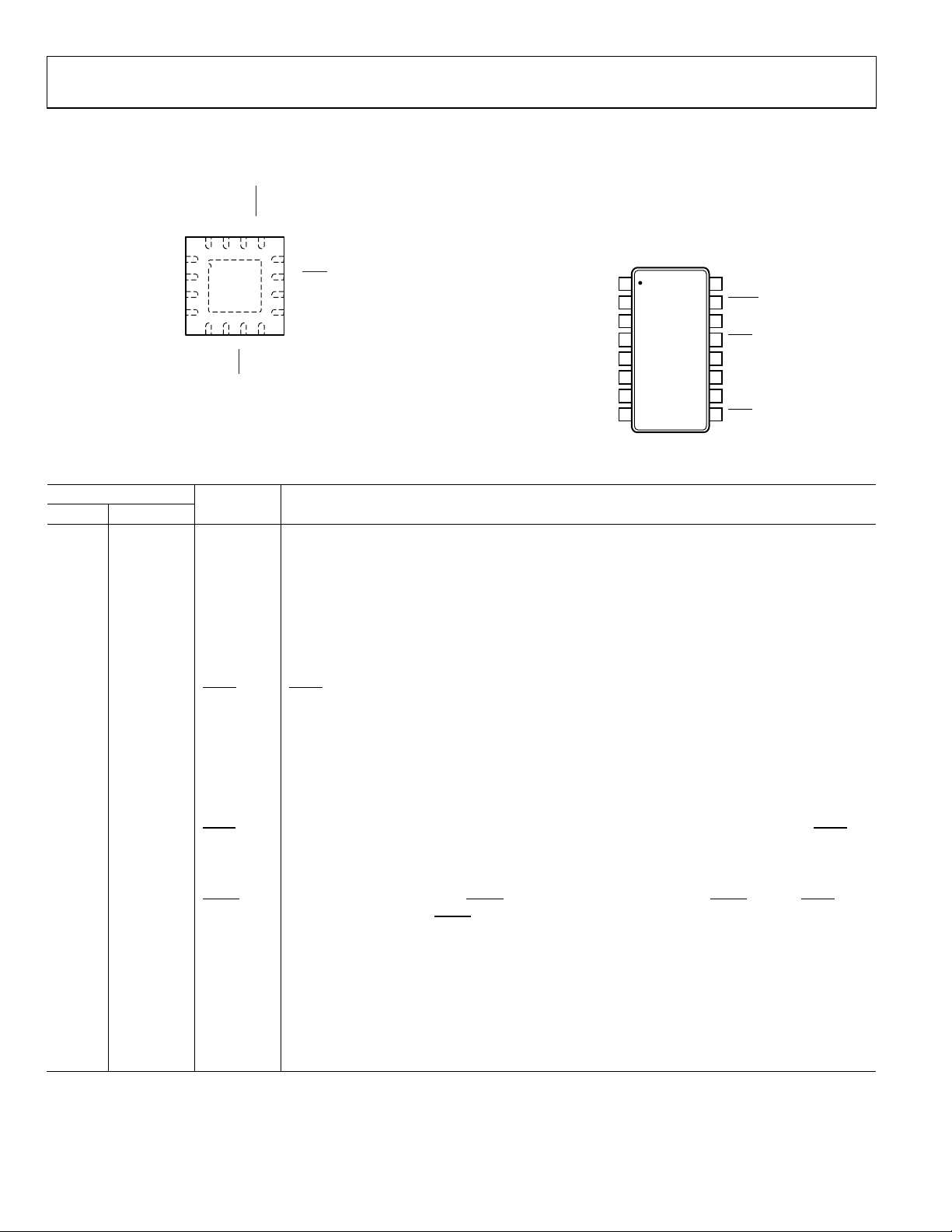
AD5686R/AD5685R/AD5684R
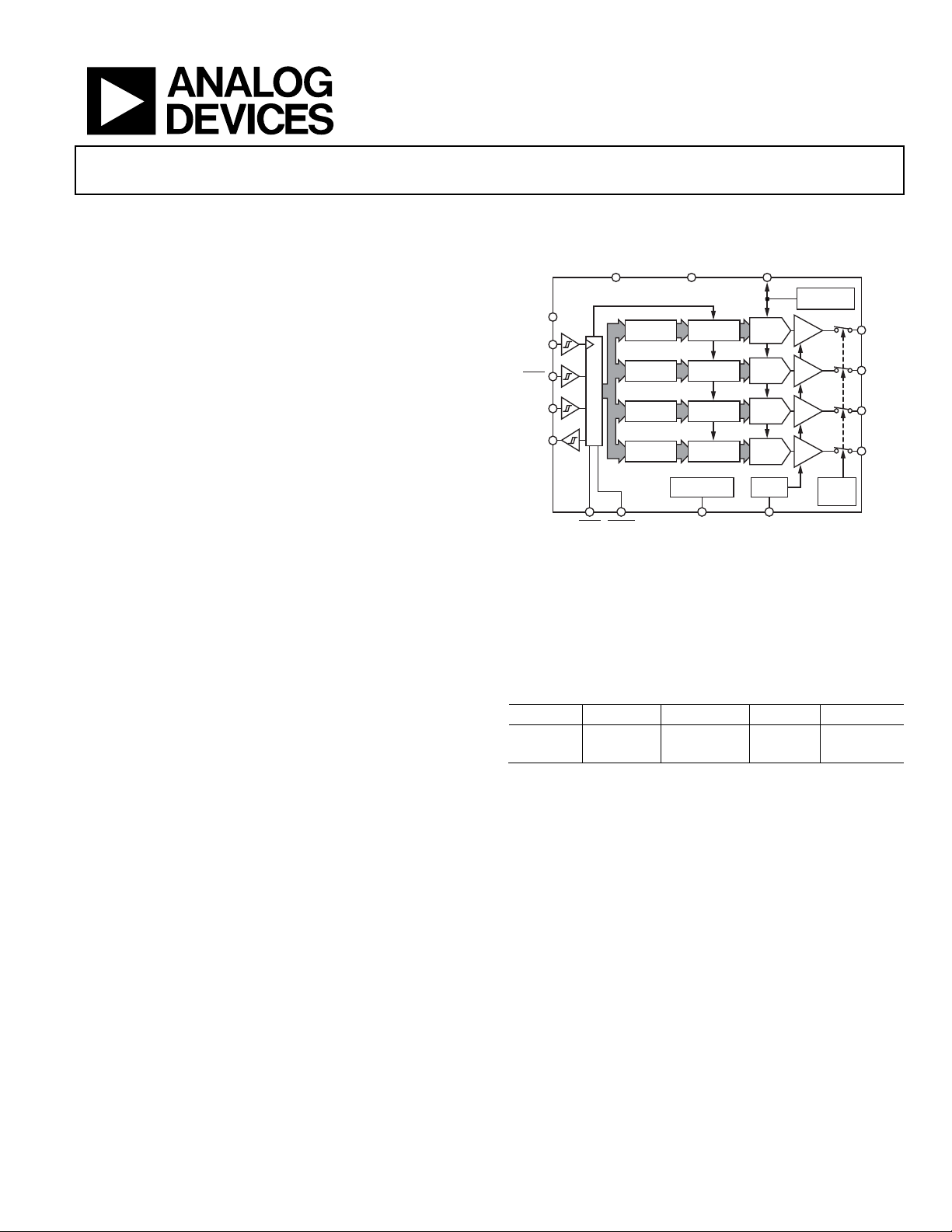
FUNCTIONAL BLOCK DIAGRAM
V
LOGIC
SCLK
SYNC
DD
AD5686R/AD5685R/AD5684R
SDIN
INTERFACE LOGIC
SDO
INPUT
REGISTER
INPUT
REGISTER
INPUT
REGISTER
INPUT
REGISTER
GND
DAC
REGISTER
DAC
REGISTER
DAC
REGISTER
DAC
REGISTER
POWER-ON
RESET
RSTSEL GAINLDAC RESET
Figure 1.
REF
STRING
DAC A
STRING
DAC B
STRING
DAC C
STRING
DAC D
GAIN
×1/×2
2.5V
REFERENCE
BUFFER
BUFFER
BUFFER
BUFFER
POWER-
DOWN
LOGIC
V
A
OUT
V
B
OUT
V
C
OUT
V
D
OUT
10485-001
GENERAL DESCRIPTION
The AD5686R/AD5685R/AD5684R, members of the
nanoDAC+® family, are low power, quad, 16-/14-/12-bit
buffered voltage output DACs. The devices include a 2.5 V,
2 ppm/°C internal reference (enabled by default) and a gain
select pin giving a full-scale output of 2.5 V (gain = 1) or 5 V
(gain = 2). All devices operate from a single 2.7 V to 5.5 V
supply, are guaranteed monotonic by design, and exhibit less
than 0.1% FSR gain error and 1.5 mV offset error performance.
The devices are available in a 3 mm × 3 mm LFCSP and a
TSSOP package.
The AD5686R/AD5685R/AD5684R also incorporate a poweron reset circuit and a RSTSEL pin that ensures that the DAC
outputs power up to zero scale or midscale and remains there
until a valid write takes place. Each part contains a per-channel
power-down feature that reduces the current consumption of
the device to 4 μA at 3 V while in power-down mode.
The AD5686R/AD5685R/AD5684R employ a versatile SPI
interface that operates at clock rates up to 50 MHz, and all
devices contain a V
Rev. 0
Information furnished by Analog Devices is believed to be accurate and reliable. However, no
responsibility is assumed by Analog Devices for its use, nor for any infringements of patents or other
rights of third parties that may result from its use. Specifications subject to change without notice. No
license is granted by implication or otherwise under any patent or patent rights of Analog Devices.
Trademarks and registered trademarks are the property of their respective owners.
pin intended for 1.8 V/3 V/5 V logic.
LOGIC
Table 1. Quad nanoDAC+ Devices
Interface Reference 16-Bit 14-Bit 12-Bit
SPI Internal AD5686R AD5685R AD5684R
I2C Internal AD5696R AD5695R AD5694R
PRODUCT HIGHLIGHTS
1. High Relative Accuracy (INL).
AD5686R (16-bit): ±2 LSB maximum
AD5685R (14-bit): ±1 LSB maximum
AD5684R (12-bit): ±1 LSB maximum
2. Low Drift 2.5 V On-Chip Reference.
2 ppm/°C typical temperature coefficient
5 ppm/°C maximum temperature coefficient
3. Two Pa ckage Opti ons .
3 mm × 3 mm, 16-lead LFCSP
16-lead TSSOP
One Technology Way, P.O. Box 9106, Norwood, MA 02062-9106, U.S.A.
Tel: 781.329.4700 www.analog.com
Fax: 781.461.3113 ©2012 Analog Devices, Inc. All rights reserved.

AD5686R/AD5685R/AD5684R Data Sheet
TABLE OF CONTENTS
Features .............................................................................................. 1
Applications ....................................................................................... 1
Functional Block Diagram .............................................................. 1
General Description ......................................................................... 1
Product Highlights ........................................................................... 1
Revision History ............................................................................... 2
Specifications ..................................................................................... 3
AC Characteristics ........................................................................ 5
Timing Characteristics ................................................................ 6
Daisy-Chain and Readback Timing Characteristics ............... 7
Absolute Maximum Ratings ............................................................ 9
ESD Caution .................................................................................. 9
Pin Configuration and Function Descriptions ........................... 10
Typical Performance Characteristics ........................................... 11
Terminology .................................................................................... 18
Theory of Operation ...................................................................... 20
Digital-to-Analog Converter .................................................... 20
Transfer Function ....................................................................... 20
DAC Architecture ....................................................................... 20
Serial Interface ............................................................................ 21
Standalone Operation ................................................................ 22
Write and Update Commands .................................................. 22
Daisy-Chain Operation ............................................................. 23
Readback Operation .................................................................. 23
Power-Down Operation ............................................................ 24
Load DAC (Hardware
LDAC
Mask Register ................................................................. 25
Hardware Reset (
Reset Select Pin (RSTSEL) ........................................................ 26
Internal Reference Setup ........................................................... 26
Solder Heat Reflow ..................................................................... 26
Long-Term Temperature Drift ................................................. 26
Thermal Hysteresis .................................................................... 27
Applications Information .............................................................. 28
Microprocessor Interfacing ....................................................... 28
AD5686R/AD5685R/AD5684R to ADSP-BF531 Interface .. 28
AD5686R/AD5685R/AD5684R to SPORT Interface ............ 28
Layout Guidelines....................................................................... 28
Galvanically Isolated Interface ................................................. 29
Outline Dimensions ....................................................................... 30
Ordering Guide .......................................................................... 31
LDAC
Pin) ........................................... 25
) .......................................................... 26
RESET
REVISION HISTORY
4/12—Revision 0: Initial Version
Rev. 0 | Page 2 of 32

Data Sheet AD5686R/AD5685R/AD5684R
STATIC PERFORMANCE2
AD5686R
Resolution
16
16
Bits
% of
±3
±3 µV/mA
Due to load current change
Load Impedance at Rails6
25
25 Ω
See Figure 34
Power-Up Time
2.5
2.5 µs
Coming out of power-down mode;
SPECIFICATIONS
VDD = 2.7 V to 5.5 V; 1.8 V ≤ V
≤ 5.5 V; all specifications T
LOGIC
MIN
to T
, unless otherwise noted. RL = 2 kΩ; CL = 200 pF.
MAX
Table 2.
1
A Grade1
Parameter Min Typ Max Min Typ Max Unit Test Conditions/Comments
Relative Accuracy ±2 ±8 ±1 ±2 LSB Gain = 2
±2 ±8 ±1 ±3 Gain = 1
Differential Nonlinearity ±1 ±1 LSB Guaranteed monotonic by design
AD5685R
Resolution 14 14 Bits
Relative Accuracy ±0.5 ±4 ±0.5 ±1 LSB
Differential Nonlinearity ±1 ±1 LSB Guaranteed monotonic by design
AD5684R
Resolution 12 12 Bits
Relative Accuracy ±0.12 ±2 ±0.12 ±1 LSB
Differential Nonlinearity ±1 ±1 LSB Guaranteed monotonic by design
Zero-Code Error 0.4 4 0.4 1.5 mV All zeros loaded to DAC register
Offset Error +0.1 ±4 +0.1 ±1.5 mV
Full-Scale Error +0.01 ±0.2 +0.01 ±0.1
Gain Error ±0.02 ±0.2 ±0.02 ±0.1
Total Unadjusted Error ±0.01 ±0.25 ±0.01 ±0.1
±0.25 ±0.2
Offset Error Drift
Gain Temperature
Coefficient
DC Power Supply Rejection
Ratio
3
3
3
DC Crosstalk3
±1 ±1 µV/°C
±1 ±1 ppm Of FSR/°C
0.15 0.15 mV/V DAC code = midscale; V
±2 ±2 µV
B Grade
% of
FSR
% of
FSR
% of
FSR
FSR
All ones loaded to DAC register
External reference; gain = 2; TSSOP
Internal reference; gain = 1; TSSOP
= 5 V ± 10%
DD
Due to single channel, full-scale
output change
±2 ±2 µV Due to powering do wn (per channel)
OUTPUT CHARACTERISTICS3
Output Voltage Range 0 V
0 2 × V
Capacitive Load Stability 2 2 nF RL = ∞
10 10 nF RL = 1 kΩ
Resistive Load4 1 1 kΩ
Load Regulation 80 80 µV/mA
80 80 µV/mA
Short-Circuit Current5 40 40 mA
0 V
REF
0 2 × V
REF
Rev. 0 | Page 3 of 32
V Gain = 1
REF
V Gain = 2, see Figure 34
REF
5 V ± 10%, DAC code = midscale;
−30 mA ≤ I
3 V ± 10%, DAC code = midscale;
−20 mA ≤ I
VDD = 5 V
≤ 30 mA
OUT
≤ 20 mA
OUT

AD5686R/AD5685R/AD5684R Data Sheet
8, 9
20
20
µ
At ambient
125
125 ppm
First cycle
Pin Capacitance
2 2 pF
I
3
3
µ
1
A Grade1
B Grade
Parameter Min Typ Max Min Typ Max Unit Test Conditions/Comments
REFERENCE OUTPUT
Output Voltage7 2.4975 2.5025 2.4975 2.5025 V At ambient
Reference TC
Output Impedance3
Output Voltage Noise3
Output Voltage Noise
Density
Load Regulation Sourcing3
Load Regulation Sinking3
Output Current Load
Capability
Line Regulation3
Long-Term Stability/Drift3
5 20 2 5 ppm/°C See the Terminology section
0.04 0.04 Ω
12 12
3
3
240 240 nV/√Hz
40
±5
40
mA VDD ≥ 3 V
±5
µV p-p
V/mA
µV/mA
0.1 Hz to 10 Hz
At ambient; f = 10 kHz, C
At ambient
100 100 µV/V At ambient
12 12 ppm After 1000 hours at 125°C
= 10 nF
L
Thermal Hysteresis3
25 25 ppm Additional cycles
LOGIC INPUTS3
Input Current ±2 ±2 µA Per pin
V
, Input Low Voltage 0.3 × V
INL
V
, Input High Voltage 0.7 × V
INH
LOGIC OUTPUTS (SDO)3
0.7 × V
LOGIC
Output Low Voltage, VOL 0.4 0.4 V
Output High Voltage, VOH V
Floating State Output
− 0.4 V
LOGIC
4 4 pF
0.3 × V
LOGIC
V
LOGIC
− 0.4 V
LOGIC
V
LOGIC
= 200 μA
I
SINK
I
SOUR CE
= 200 μA
Capacitance
POWER REQUIREMENTS
V
LOGIC
LOGIC
1.8 5.5 1.8 5.5 V
A
VDD 2.7 5.5 2.7 5.5 V Gain = 1
VDD V
+ 1.5 5.5 V
REF
+ 1.5 5.5 V Gain = 2
REF
IDD VIH = VDD, VIL = GND, VDD = 2.7 V to 5.5 V
Normal Mode10 0.59 0.7 0.59 0.7 mA Internal reference off
1.1 1.3 1.1 1.3 mA Internal reference on, at full scale
All Power-Down
11
Modes
1 4 1 4 µA −40°C to +85°C
6 6 µA −40°C to +105°C
1
Temperature range: A and B grade: −40°C to +105°C.
2
DC specifications tested with the outputs unloaded, unless otherwise noted. Upper dead band = 10 mV and exists only when V
with gain = 2. Linearity calculated using a reduced code range of 256 to 65,280 (AD5686R), 64 to 16,320 (AD5685R), and 12 to 4080 (AD5684R).
V
DD
3
Guaranteed by design and characterization; not production tested.
4
Channel A and Channel B can have a combined output current of up to 30 mA. Similarly, Channel C and Channel D can have a combined output current of up to
30 mA up to a junction temperature of 110°C.
5
VDD = 5 V. The device includes current limiting that is intended to protect the device during temporary overload conditions. Junction temperature can be exceeded
during current limit. Operation above the specified maximum operation junction temperature may impair device reliability.
6
When drawing a load current at either rail, the output voltage headroom with respect to that rail is limited by the 25 Ω typical channel resistance of the output
devices. For example, when sinking 1 mA, the minimum output voltage = 25 Ω × 1 mA = 25 mV (see
7
Initial accuracy presolder reflow is ±750 µV; output voltage includes the effects of preconditioning drift. See the Internal Reference Setup section.
8
Reference is trimmed and tested at two temperatures and is characterized from −40°C to +105°C.
9
Reference temperature coefficient calculated as per the box method. See the Terminology section for further information.
10
Interface inactive. All DACs active. DAC outputs unloaded.
11
All DACs powered down.
Figure 34).
= VDD with gain = 1 or when V
REF
REF
/2 =
Rev. 0 | Page 4 of 32

Data Sheet AD5686R/AD5685R/AD5684R
Total Harmonic Distortion4
−80 dB
At ambient, BW = 20 kHz, VDD = 5 V, f
= 1 kHz
AC CHARACTERISTICS
VDD = 2.7 V to 5.5 V; RL = 2 kΩ to GND; CL = 200 pF to GND; 1.8 V ≤ V
1
noted.
Table 3.
Parameter2 Min Typ Max Unit Test Conditions/Comments3
Output Voltage Settling Time
AD5686R 5 8 µs ¼ to ¾ scale settling to ±2 LSB
AD5685R 5 8 µs ¼ to ¾ scale settling to ±2 LSB
AD5684R 5 7 µs ¼ to ¾ scale settling to ±2 LSB
Slew Rate 0.8 V/µs
Digital-to-Analog Glitch Impulse 0.5 nV-sec 1 LSB change around major carry
Digital Feedthrough 0.13 nV-sec
Digital Crosstalk 0.1 nV-sec
Analog Crosstalk 0.2 nV-sec
DAC-to-DAC Crosstalk 0.3 nV-sec
Output Noise Spectral Density 300 nV/√Hz DAC code = midscale, 10 kHz; gain = 2
Output Noise 6 µV p-p 0.1 Hz to 10 Hz
SNR 90 dB At ambient, BW = 20 kHz, VDD = 5 V, f
SFDR 83 dB At ambient, BW = 20 kHz, VDD = 5 V, f
SINAD 80 dB At ambient, BW = 20 kHz, VDD = 5 V, f
1
Guaranteed by design and characterization, not production tested.
2
See the Terminology section.
3
Temperature range is −40°C to +105°C, typical @ 25°C.
4
Digitally generated sine wave @ 1 kHz.
≤ 5.5 V; all specifications T
LOGIC
MIN
to T
, unless otherwise
MAX
OUT
= 1 kHz
OUT
= 1 kHz
OUT
= 1 kHz
OUT
Rev. 0 | Page 5 of 32
AD5686R/AD5685R/AD5684R Data Sheet
Minimum
High Time (Single, Combined or All Channel Update)
t8
20 20 ns
t
4
t
3
SCLK
SYNC
SDIN
t
1
t
2
t
5
t
6
t
7
t
8
DB23
t
9
t
10
t
11
LDAC
1
LDAC
2
t
12
1
ASYNCHRONOUS LDAC UPDATE MODE .
2
SYNCHRONOUS LDAC UPDATE MODE .
RESET
t
13
t
14
V
OUT
DB0
10485-002
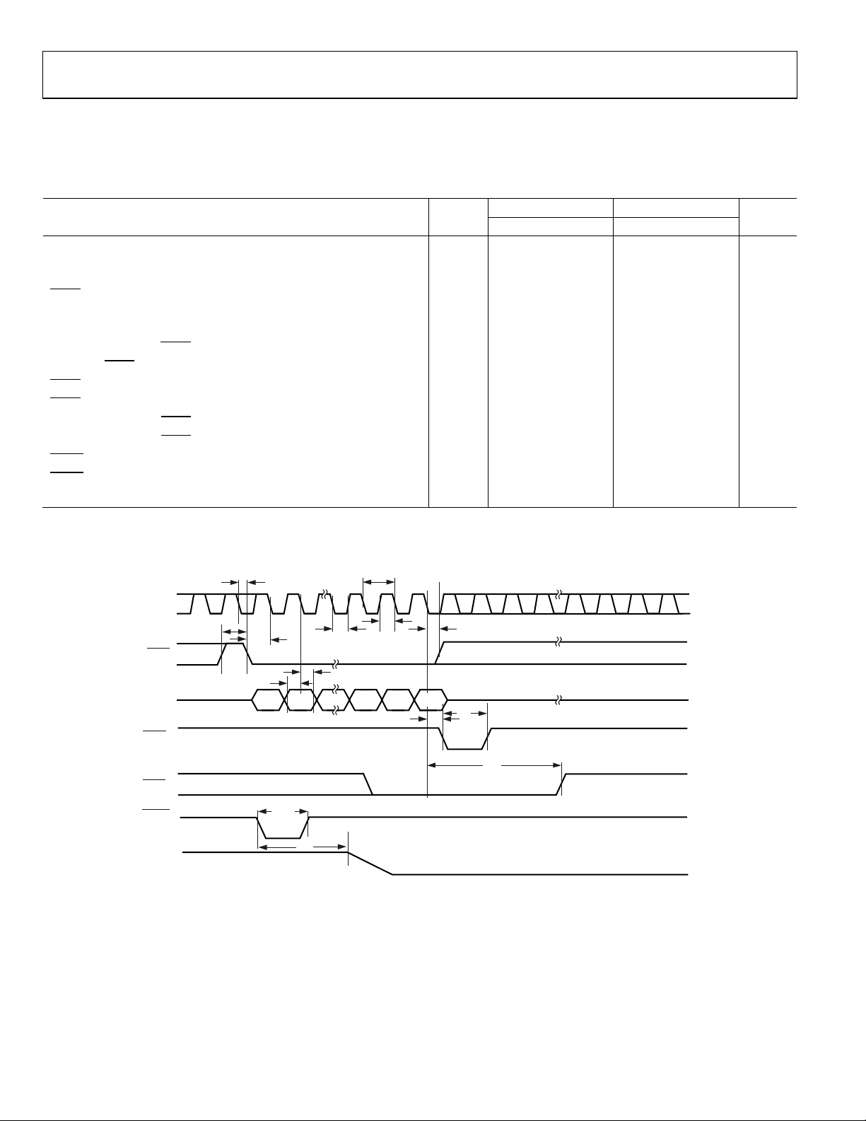
TIMING CHARACTERISTICS
All input signals are specified with tR = tF = 1 ns/V (10% to 90% of VDD) and timed from a voltage level of (VIL + VIH)/2. See Figure 2.
V
= 2.7 V to 5.5 V, 1.8 V ≤ V
DD
Table 4.
Parameter1 Symbol Min Max Min Max Unit
SCLK Cycle Time t1 33 20 ns
SCLK High Time t2 16 10 ns
SCLK Low Time t3 16 10 ns
to SCLK Falling Edge Setup Time t4 15 10 ns
SYNC
Data Setup Time t5 5 5 ns
Data Hold Time t6 5 5 ns
SCLK Falling Edge to
Rising Edge t7 15 10 ns
SYNC
SYNC
Falling Edge to SCLK Fall Ignore t9 16 10 ns
SYNC
Pulse Width Low t10 25 15 ns
LDAC
SCLK Falling Edge to
SCLK Falling Edge to
Minimum Pulse Width Low t13 30 30 ns
RESET
Pulse Activation Time t14 30 30 ns
RESET
Rising Edge t11 30 20 ns
LDAC
Falling Edge t12 20 20 ns
LDAC
Power-Up Time2 4.5 4.5 µs
1
Maximum SCLK frequency is 50 MHz at VDD = 2.7 V to 5.5 V, 1.8 V ≤ V
2
Time to exit power-down to normal mode of AD5686R/AD5685R/AD5684R operation, 32nd clock edge to 90% of DAC midscale value, with output unloaded.
LOGIC
≤ 5.5 V; V
= 2.5 V. All specifications T
REFIN
≤ VDD. Guaranteed by design and characterization; not production tested.
LOGIC
MIN
to T
1.8 V ≤ V
, unless otherwise noted.
MAX
< 2.7 V 2.7 V ≤ V
LOGIC
LOGIC
≤ 5.5 V
Figure 2. Serial Write Operation
Rev. 0 | Page 6 of 32
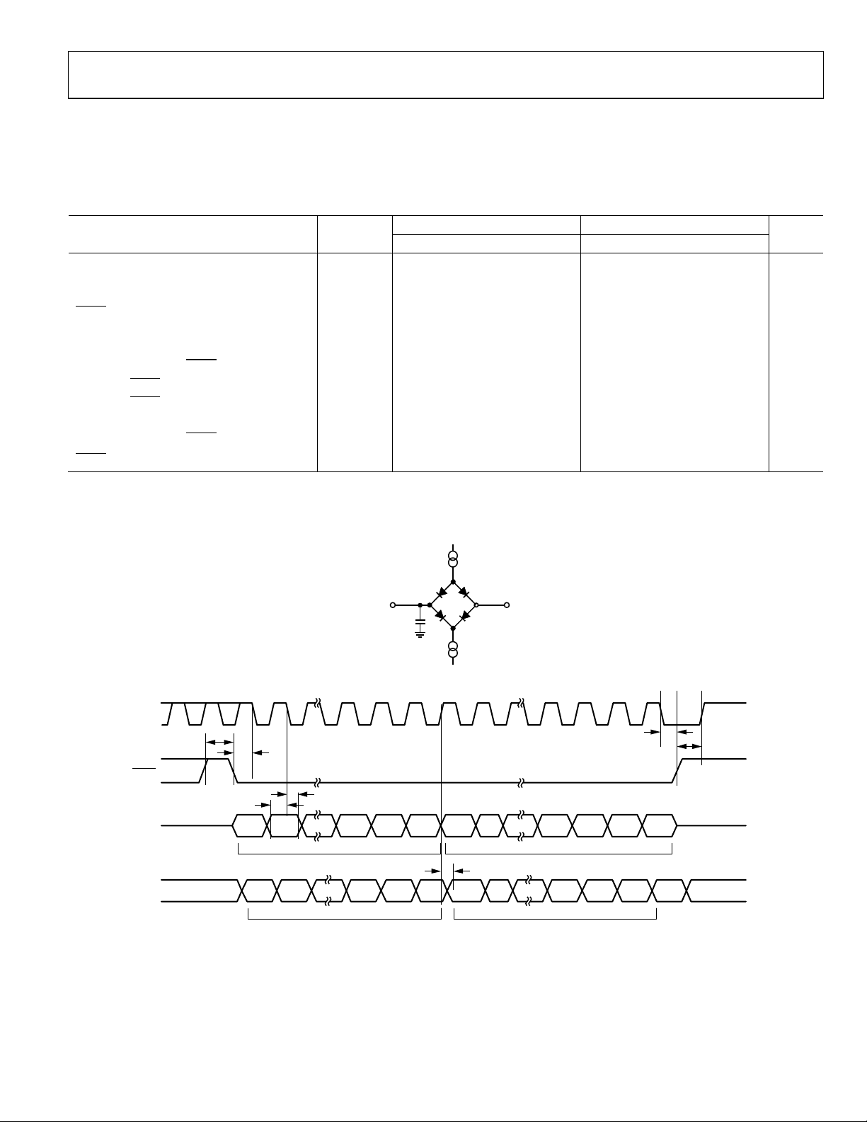
Data Sheet AD5686R/AD5685R/AD5684R
SCLK High Time
t2
33 20 ns
10485-003
200µA I
OL
200µA I
OH
V
OH
(MIN)
TO OUTPUT
PIN
C
L
20pF
t
4
t
5
t
6
t
8
SDO
SDIN
SYNC
SCLK
4824
DB23 DB0 DB23 DB0
DB23
INPUT WORD FOR DAC NUNDEFINED
INPUT WORD FOR DAC N + 1INPUT WORD FOR DAC N
DB0
t
11
t
12
t
10
10485-004
DAISY-CHAIN AND READBACK TIMING CHARACTERISTICS
All input signals are specified with tR = tF = 1 ns/V (10% to 90% of VDD) and timed from a voltage level of (VIL + VIH)/2. See Figure 4
and Figure 5. V
2.7 V to 5.5 V.
Table 5.
1.8 V ≤ V
Parameter1 Symbol Min Max Min Max Unit
SCLK Cycle Time t1 66 40 ns
SCLK Low Time t3 33 20 ns
to SCLK Falling Edge t4 33 20 ns
SYNC
Data Setup Time t5 5 5 ns
Data Hold Time t6 5 5 ns
SCLK Falling Edge to
Minimum
Minimum
SDO Data Valid from SCLK Rising Edge t10 36 25 ns
SCLK Falling Edge to
Rising Edge to SCLK Rising Edge t
SYNC
1
Maximum SCLK frequency is 25 MHz or 15 MHz at VDD = 2.7 V to 5.5 V, 1.8 V ≤ V
Circuit and Timing Diagrams
= 2.7 V to 5.5 V, 1.8 V ≤ V
DD
Rising Edge t7 15 10 ns
SYNC
High Time t8 60 30 ns
SYNC
High Time t9 60 30 ns
SYNC
Rising Edge t
SYNC
≤ 5.5 V; V
LOG IC
5
15 10 ns
11
5
15 10 ns
12
= 2.5 V. All specifications T
REF
< 2.7 V 2.7 V ≤ V
LOGIC
≤ VDD. Guaranteed by design and characterization; not production tested.
LOGIC
MIN
to T
, unless otherwise noted. VDD =
MAX
≤ 5.5 V
LOGIC
Figure 3. Load Circuit for Digital Output (SDO) Timing Specifications
Figure 4. Daisy-Chain Timing Diagram
Rev. 0 | Page 7 of 32
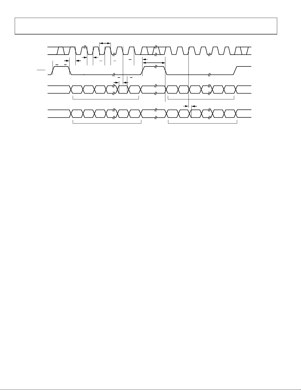
AD5686R/AD5685R/AD5684R Data Sheet
10485-005
SYNC
t
8
t
6
SCLK
24
1
24
1
t
9
t
4
t
2
t
7
t
3
t
1
DB23 DB0 DB23 DB0
SDIN
NOP CONDITIONINPUT WORD SPECIFIES
REGIST E R TO BE READ
t
5
DB23 DB0 DB23 DB0
SDO
SELECTED REGISTER DATA
CLOCKED OUT
UNDEFINED
t
10
Figure 5. Readback Timing Diagram
Rev. 0 | Page 8 of 32
Data Sheet AD5686R/AD5685R/AD5684R
Storage Temperature Range
−65°C to +150°C
Reflow Soldering Peak
260°C
ABSOLUTE MAXIMUM RATINGS
TA = 25°C, unless otherwise noted.
Table 5.
Parameter Rating
VDD to GND −0.3 V to +7 V
V
to GND −0.3 V to +7 V
LOGIC
V
to GND −0.3 V to VDD + 0.3 V
OUT
V
to GND −0.3 V to VDD + 0.3 V
REF
Digital Input Voltage to GND −0.3 V to V
Operating Temperature Range −40°C to +105°C
Junction Temperature 125°C
16-Lead TSSOP, θJA Thermal
Impedance, 0 Airflow (4-Layer Board)
16-Lead LFCSP, θJA Thermal
Impedance, 0 Airflow (4-Layer Board)
112.6°C/W
70°C/W
LOGIC
+ 0.3 V
Stresses above those listed under Absolute Maximum Ratings
may cause permanent damage to the device. This is a stress
rating only; functional operation of the device at these or any
other conditions above those indicated in the operational
section of this specification is not implied. Exposure to absolute
maximum rating conditions for extended periods may affect
device reliability.
ESD CAUTION
Temperature, Pb Free (J-STD-020)
ESD1 4 kV
FICDM 1.5 kV
1
Human body model (HBM) classification.
Rev. 0 | Page 9 of 32
AD5686R/AD5685R/AD5684R Data Sheet
Pin No.
12
14
SDIN
Serial Data Input. This device has a 24-bit input shift register. Data is clocked into the register on the
Power-On Reset Pin. Tying this pin to GND powers up all four DACs to zero scale. Tying this pin to
VDD powers up all four DACs to midscale.
12
11
10
1
3
4
SDIN
SYNC
SCLK
9
V
LOGIC
V
OUT
A
V
DD
2
GND
V
OUT
C
6
SDO
5
V
OUT
D
7
LDAC
8
GAIN
16
V
OUT
B
15
V
REF
14
RSTSEL
13
RESET
AD5686R/AD5685R/AD5684R
NOTES
1. THE EXPOSED PAD MUST BE TIED TO GND.
TOP VIEW
(Not to S cale)
10485-006
1
2
3
4
5
6
7
8
V
OUT
B
V
OUT
A
GND
V
OUT
D
V
OUT
C
V
DD
V
REF
SDO
16
15
14
13
12
11
10
9
RESET
SDIN
SYNC
GAIN
LDAC
V
LOGIC
SCLK
RSTSEL
TOP VIEW
(Not to S cale)
AD5686R/
AD5685R/
AD5684R
10485-007
PIN CONFIGURATION AND FUNCTION DESCRIPTIONS
Figure 6. 16-Lead LFCSP Pin Configuration
Table 6. Pin Function Descriptions
Mnemonic Description LFCSP TSSOP
1 3 V
A Analog Output Voltage from DAC A. The output amplifier has rail-to-rail operation.
OUT
2 4 GND Ground Reference Point for All Circuitry on the Part.
3 5 VDD Power Supply Input. These parts can be operated from 2.7 V to 5.5 V, and the supply should be
decoupled with a 10 µF capacitor in parallel with a 0.1 µF capacitor to GND.
4 6 V
5 7 V
C Analog Output Voltage from DAC C. The output amplifier has rail-to-rail operation.
OUT
D Analog Output Voltage from DAC D. The output amplifier has rail-to-rail operation.
OUT
6 8 SDO Serial Data Output. Can be used to daisy-chain a number of AD5686R/AD5685R/AD5684R devices
together or can be used for readback. The serial data is transferred on the rising edge of SCLK and is
valid on the falling edge of the clock.
7 9
LDAC
can be operated in two modes, asynchronously and synchronously. Pulsing this pin low allows
LDAC
any or all DAC registers to be updated if the input registers have new data. This allows all DAC outputs
to simultaneously update. This pin can also be tied permanently low.
8 10 GAIN Span Set Pin. When this pin is tied to GND, all four DAC outputs have a span from 0 V to V
9 11 V
pin is tied to V
Digital Power Supply. Voltage ranges from 1.8 V to 5.5 V.
LOGIC
, all four DACs output a span of 0 V to 2 × V
DD
10 12 SCLK Serial Clock Input. Data is clocked into the input shift register on the falling edge of the serial clock
input. Data can be transferred at rates of up to 50 MHz.
11 13
Active Low Control Input. This is the frame synchronization signal for the input data. When
SYNC
goes low, data is transferred in on the falling edges of the next 24 clocks.
falling edge of the serial clock input.
13 15
Asynchronous Reset Input. The
RESET
pulses are ignored. When
input is falling edge sensitive. When
RESET
is activated, the input register and the DAC register are updated with
RESET
zero scale or midscale, depending on the state of the RSTSEL pin.
14 16 RSTSEL
15 1 V
16 2 V
17 N/A EPAD Exposed Pad. The exposed pad must be tied to GND.
Reference Voltage. The AD5686R/AD5685R/AD5684R have a common reference pin. When using
REF
the internal reference, this is the reference output pin. When using an external reference, this is the
reference input pin. The default for this pin is as a reference output.
B Analog Output Voltage from DAC B. The output amplifier has rail-to-rail operation.
OUT
Rev. 0 | Page 10 of 32
Figure 7. 16-Lead TSSOP Pin Configuration
.
REF
is low, all
RESET
. If this
REF
SYNC
LDAC

Data Sheet AD5686R/AD5685R/AD5684R
–40 –20 0 20 40 60 80 100 120
V
REF
(V)
TEMPERATURE (°C)
DEVICE 1
DEVICE 2
DEVICE 3
DEVICE 4
DEVICE 5
10485-212
2.4980
2.4985
2.4990
2.4995
2.5000
2.5005
2.5010
2.5015
2.5020
V
DD
= 5V
–40 –20 0 20 40 60 80 120100
V
REF
(V)
TEMPERATURE (°C)
DEVICE 1
DEVICE 2
DEVICE 3
DEVICE 4
DEVICE 5
10485-109
2.4980
2.4985
2.4990
2.4995
2.5000
2.5005
2.5010
2.5015
2.5020
VDD = 5V
90
0
10
20
30
40
50
60
70
80
0 0.5 1.0 1.5 2.0 2.5 3.0 3.5 4.0 4.5 5.0
NUMBER OF UNI TS
TEMPERAT URE DRIFT (p pm/°C)
10485-250
V
DD
= 5V
60
0
10
20
30
40
50
2.498 2.499 2.500 2.501 2.502
HITS
V
REF
(V)
0 HOUR
168 HOURS
500 HOURS
1000 HOURS
10485-251
V
DD
= 5.5V
1600
0
200
400
600
800
1000
1200
1400
10 100 1k 10k 100k 1M
NSD (nV/ Hz)
FREQUENCY (MHz)
10485-111
V
DD
= 5V
T
A
= 25°C
CH1 10µV M1.0s A CH1 160mV
1
T
10485-112
VDD = 5V
T
A
= 25°C
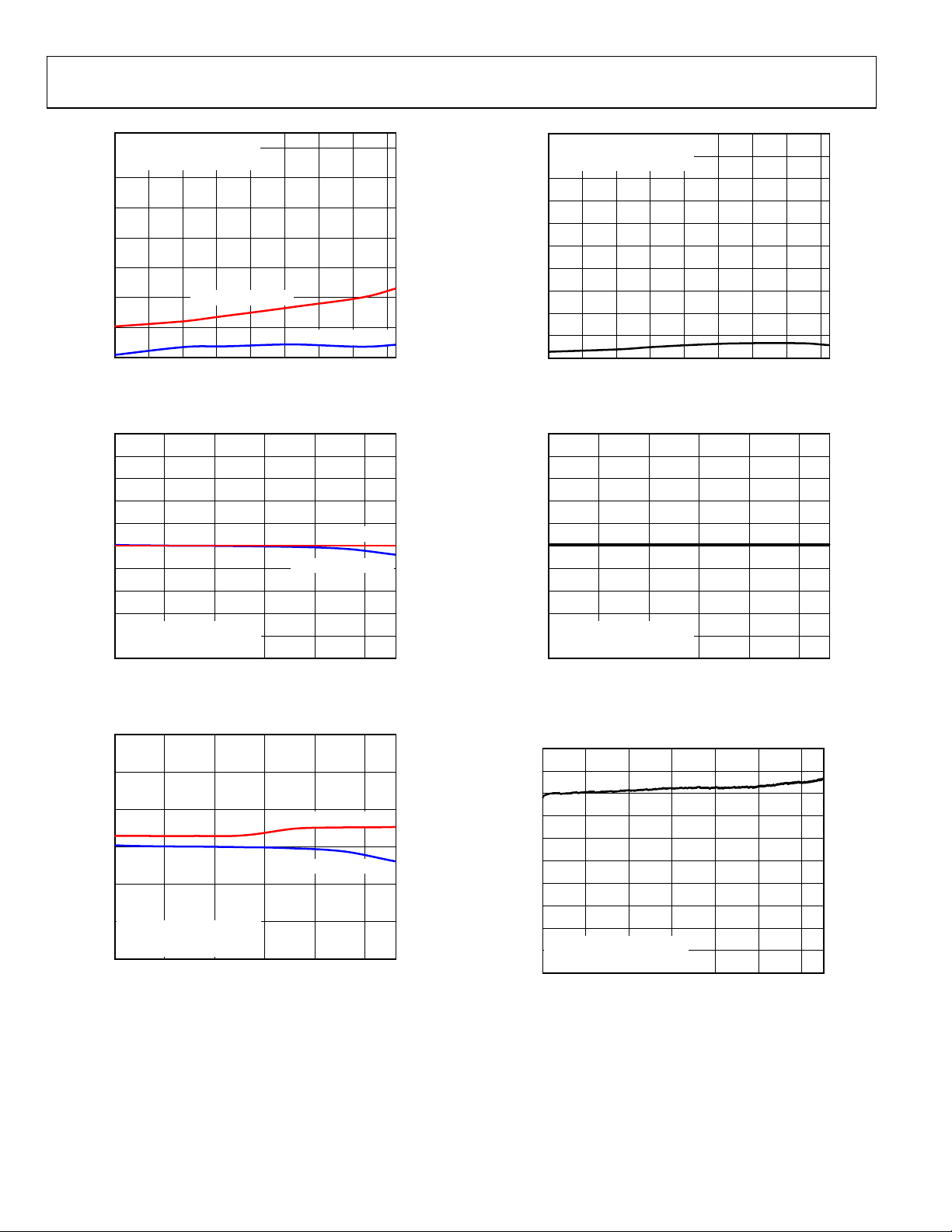
TYPICAL PERFORMANCE CHARACTERISTICS
Figure 8. Internal Reference Voltage vs. Temperature (Grade B)
Figure 9. Internal Reference Voltage vs. Temperature (Grade A)
Figure 11. Reference Long-Term Stability/Drift
Figure 12. Internal Reference Noise Spectral Density vs. Frequency
Figure 10. Reference Output Temperature Drift Histogram
Figure 13. Internal Reference Noise, 0.1 Hz to 10 Hz
Rev. 0 | Page 11 of 32

AD5686R/AD5685R/AD5684R Data Sheet
2.5000
2.4999
2.4998
2.4997
2.4996
2.4995
2.4994
2.4993
–0.005 –0.003 –0.001 0.001 0.003 0.005
V
REF
(V)
I
LOAD
(A)
10485-113
VDD = 5V
T
A
= 25°C
2.5002
2.5000
2.4998
2.4996
2.4994
2.4992
2.4990
2.5 3.0 3.5 4.0 4.5 5.0 5.5
V
REF
(V)
VDD (V)
D1
D3
D2
10485-117
TA = 25°C
10
–10
–8
–6
–4
–2
0
2
4
8
6
0 10000 20000 30000 40000 50000 60000
INL (LSB)
CODE
10485-118
VDD = 5V
T
A
= 25°C
INTERNAL RE FERENCE = 2.5V
10
–10
–8
–6
–4
–2
0
2
4
8
6
0 2500 5000 7500 10000 12500 1500016348
INL (LSB)
CODE
10485-119
V
DD
= 5V
T
A
= 25°C
INTERNAL RE FERENCE = 2.5V
10
–10
–8
–6
–4
–2
0
2
4
8
6
0 625 1250 1875 2500 3125 3750 4096
INL (LSB)
CODE
10485-120
VDD = 5V
T
A
= 25°C
INTERNAL RE FERENCE = 2.5V
1.0
–1.0
–0.8
–0.6
–0.4
–0.2
0
0.2
0.4
0.8
0.6
0 10000 20000 30000 40000 50000 60000
DNL (LSB)
CODE
10485-121
VDD = 5V
T
A
= 25°C
INTERNAL RE FERENCE = 2.5V
Figure 14. Internal Reference Voltage vs. Load Current
Figure 15. Internal Reference Voltage vs. Supply Voltage
Figure 17. AD5685R INL
Figure 18. AD5684R INL
Figure 16. AD5686R INL
Figure 19. AD5686R DNL
Rev. 0 | Page 12 of 32

Data Sheet AD5686R/AD5685R/AD5684R
1.0
0.8
0.6
0.4
0.2
0
DNL (LSB)
–0.2
–0.4
–0.6
VDD = 5V
–0.8
= 25°C
T
A
INTERNAL REFERENCE = 2.5V
–1.0
0 2500 5000 7500 10000 12500 15000 16383
CODE
Figure 20. AD5685R DNL
10485-122
10
8
6
4
2
0
–2
ERROR (LSB)
–4
–6
VDD = 5V
–8
= 25°C
T
A
INTERNAL REFERENCE = 2.5V
–10
05.04.54.03.53.02.52.01.51.00.5
Figure 23. INL Error and DNL Error vs. V
INL
DNL
V
(V)
REF
REF
10485-125
1.0
0.8
0.6
0.4
0.2
0
DNL (LS B)
–0.2
–0.4
–0.6
VDD = 5V
–0.8
T
= 25°C
A
INTERNAL REFERENCE = 2.5V
–1.0
0 625 1250 1875 2500 3125 3750 4096
CODE
Figure 21. AD5684R DNL
10
8
6
4
2
0
–2
ERROR (LSB)
–4
–6
VDD = 5V
–8
= 25°C
T
A
INTERNAL REFERENCE = 2.5V
–10
–40 1106010
INL
DNL
TEMPERATURE (°C)
Figure 22. INL Error and DNL Error vs. Temperature
10
8
6
4
2
0
–2
ERROR (LSB)
–4
–6
VDD = 5V
–8
= 25°C
T
A
INTERNAL REFERENCE = 2.5V
–10
2.7 5.24.74.23.73.2
10485-123
SUPPLY VOLTAGE (V)
INL
DNL
10485-126
Figure 24. INL Error and DNL Error vs. Supply Voltage
0.10
0.08
0.06
0.04
0.02
0
–0.02
ERROR (% of F S R )
–0.04
–0.06
VDD = 5V
–0.08
= 25°C
T
A
INTERNAL REFERENCE = 2.5V
–0.10
–40–200 20406080100120
10485-124
FULL-SCALE ERROR
GAIN ERROR
TEMPERATURE (°C)
10485-127
Figure 25. Gain Error and Full-Scale Error vs. Temperature
Rev. 0 | Page 13 of 32
AD5686R/AD5685R/AD5684R Data Sheet
1.4
1.2
1.0
0.8
0.6
0.4
0.2
0
–40 –20 0 20 40 60 80 100 120
ERROR (mV)
TEMPERATURE (°C)
OFFSET ERROR
ZERO-CO DE E RROR
10485-128
VDD = 5V
T
A
= 25°C
INTERNAL RE FERENCE = 2.5V
0.10
–0.10
–0.08
–0.06
–0.04
–0.02
0
0.02
0.04
0.06
0.08
2.7 5.24.74.23.73.2
ERROR (% of FSR)
SUPPLY VOLTAGE (V)
GAIN ERROR
FULL-S CALE ERROR
10485-129
V
DD
= 5V
T
A
= 25°C
INTERNAL RE FERENCE = 2.5V
1.5
–1.5
–1.0
–0.5
0
0.5
1.0
2.7 5.24.74.23.73.2
ERROR (mV)
SUPPLY VOLTAGE (V)
ZERO-CO DE E RROR
OFFSET ERROR
10485-130
V
DD
= 5V
T
A
= 25°C
INTERNAL RE FERENCE = 2.5V
0.10
0.09
0.08
0.07
0.06
0.05
0.04
0.03
0.02
0.01
0
–40 –20 0 20 40 60 80 100 120
TOTAL UNADJUS TED ERROR (% of FSR)
TEMPERATURE (°C)
10485-131
VDD = 5V
T
A
= 25°C
INTERNAL RE FERENCE = 2.5V
0.10
0.08
0.06
0.04
0.02
0
–0.02
–0.04
–0.06
–0.08
–0.10
2.7 5.24.74.23.73.2
TOTAL UNADJUS TED ERROR (% of FSR)
SUPPLY VOLTAGE (V)
10485-132
VDD = 5V
T
A
= 25°C
INTERNAL RE FERENCE = 2.5V
0
TOTAL UNADJUS TED ERROR (% of FSR)
10485-133
Figure 26. Zero-Code Error and Offset Error vs. Temperature
Figure 27. Gain Error and Full-Scale Error vs. Supply
Figure 28. Zero-Code Error and Offset Error vs. Supply
Figure 29. TUE vs. Temperature
Figure 30. TUE vs. Supply, Gain = 1
–0.01
–0.02
–0.03
–0.04
–0.05
–0.06
–0.07
–0.08
VDD = 5V
–0.09
= 25°C
T
A
INTERNAL RE FERENCE = 2.5V
–0.10
0 10000 20000 30000 40000 50000 60000 65535
CODE
Figure 31. TUE vs. Code
Rev. 0 | Page 14 of 32

Data Sheet AD5686R/AD5685R/AD5684R
25
20
15
10
5
0
540 560 580 600 620 640
HITS
I
DD
(V)
10485-135
V
DD
= 5V
T
A
= 25°C
EXTERNAL
REFERENCE = 2. 5V
30
25
20
15
10
5
0
1000 1020 1040 1060 1080 1100 1120 1140
HITS
IDD FULLSCALE (V)
10485-136
V
DD
= 5V
T
A
= 25°C
INTERNAL
REFERENCE = 2.5V
1.0
–1.0
–0.8
–0.6
–0.4
–0.2
0
0.2
0.4
0.6
0.8
0 5 10 15 20 25 30
ΔV
OUT
(V)
LOAD CURRENT ( mA)
10485-200
SOURCING 2.7V
SOURCING 5V
SINKING 2.7V
SINKING 5V
7
–2
–1
0
1
2
3
4
5
6
–0.06 –0.04 –0.02 0 0.02 0.04 0.06
V
OUT
(V)
LOAD CURRENT ( A)
0xFFFF
0x4000
0x8000
0xC000
0x0000
10485-138
V
DD
= 5V
T
A
= 25°C
GAIN = 2
INTERNAL
REFERENCE = 2.5V
5
–2
–1
0
1
2
3
4
–0.06 –0.04 –0.02 0 0.02 0.04 0.06
V
OUT
(V)
LOAD CURRENT ( A)
0xFFFF
0x4000
0x8000
0xC000
0x0000
10485-139
V
DD
= 5V
T
A
= 25°C
EXTERNAL RE FERENCE = 2.5V
GAIN = 1
0
0.2
0.4
0.6
0.8
1.0
1.2
1.4
–40 1106010
CURRENT (mA)
TEMPERATURE (°C)
FULL-SCALE
ZERO CODE
EXTERNAL RE FERENCE, F ULL-SCALE
10485-140
Figure 32. IDD Histogram with External Reference, 5 V
Figure 33. IDD Histogram with Internal Reference, V
= 2.5 V, Gain = 2
REFOUT
Figure 35. Source and Sink Capability at 5 V
Figure 36. Source and Sink Capability at 3 V
Figure 34. Headroom/Footroom vs. Load Current
Figure 37. Supply Current vs. Temperature
Rev. 0 | Page 15 of 32

AD5686R/AD5685R/AD5684R Data Sheet
4.0
V
(V)
–0.01
0
0.06
0.01
0.02
0.03
0.04
0.05
–1
0
6
1
2
3
4
5
–10 15100 5–5
V
OUT
(V)
V
DD
(V)
TIME (µs)
CH D
V
DD
CH A
CH B
CH C
10485-142
TA = 25°C
INTERNAL RE FERENCE = 2.5V
0
1
3
2
–5 100 5
V
OUT
(V)
TIME (µs)
CH D
SYNC
CH A
CH B
CH C
10485-143
VDD = 5V
T
A
= 25°C
INTERNAL RE FERENCE = 2.5V
GAIN = 1
GAIN = 2
2.4988
2.5008
2.5003
2.4998
2.4993
0 128 104 62
V
OUT
(V)
TIME (µs)
10485-144
CHANNEL B
T
A
= 25°C
V
DD
= 5.25V
INTERNAL RE FERENCE
CODE = 7FF F TO 8000
ENERGY = 0. 227206nV-sec
–0.002
–0.001
0
0.001
0.002
0.003
0 252010 155
V
OUT
AC-COUPLED ( V )
TIME (µs)
CH B
CH C
CH D
10485-145
CH1 10µV M1.0s A CH1 802mV
1
T
10485-146
V
DD
= 5V
T
A
= 25°C
EXTERNAL RE FERENCE = 2.5V
DAC A
3.5
3.0
2.5
2.0
OUT
1.5
1.0
0.5
DAC B
DAC C
DAC D
VDD = 5V
= 25°C
T
A
INTERNAL RE FERENCE = 2.5V
¼ TO ¾ SCALE
0
10 32016040 8020
Figure 38. Settling Time, 5.25 V
TIME (µs)
10485-141
Figure 41. Digital-to-Analog Glitch Impulse
Figure 39. Power-On Reset to 0 V
Figure 40. Exiting Power-Down to Midscale
Figure 42. Analog Crosstalk, Channel A
Figure 43. 0.1 Hz to 10 Hz Output Noise Plot, External Reference
Rev. 0 | Page 16 of 32

Data Sheet AD5686R/AD5685R/AD5684R
CH1 10µV M1.0s A CH1 802mV
1
T
10485-147
VDD = 5V
T
A
= 25°C
INTERNAL RE FERENCE = 2.5V
0
200
400
600
800
1000
1200
1400
1600
10 1M100k1k 10k100
NSD (nV/ Hz)
FREQUENCY ( Hz )
FULL-SCALE
MIDSCALE
ZERO-SCALE
10485-148
VDD = 5V
T
A
= 25°C
INTERNAL RE FERENCE = 2.5V
–180
–160
–140
–120
–100
–80
–60
–40
–20
0
20
0 20000160008000 1200040002000 1800010000 140006000
THD (dBV)
FREQUENCY ( Hz )
10485-149
VDD = 5V
T
A
= 25°C
INTERNAL RE FERENCE = 2.5V
4.0
V
(V)
–60
–50
–40
–30
–20
–10
0
10k 10M1M100k
BANDWIDTH (dB)
FREQUENCY ( Hz )
10485-151
V
DD
= 5V
T
A
= 25°C
EXTERNAL RE FERENCE = 2.5V, ±0.1V p- p
Figure 44. 0.1 Hz to 10 Hz Output Noise Plot, 2.5 V Internal Reference
OUT
0nF
3.9
3.8
3.7
3.6
3.5
3.4
3.3
3.2
3.1
3.0
0.1nF
10nF
0.22nF
4.7nF
1.590 1.6301.6201.600 1.610 1.6251.605 1.6151.595
Figure 47. Settling Time vs. Capacitive Load
VDD = 5V
= 25°C
T
A
INTERNAL RE FERENCE = 2.5V
TIME (ms)
10485-150
Figure 45. Noise Spectral Density
Figure 46. Total Harmonic Distortion @ 1 kHz
Figure 48. Multiplying Bandwidth, External Reference = 2.5 V, ±0.1 V p-p,
10 kHz to 10 MHz
Rev. 0 | Page 17 of 32

AD5686R/AD5685R/AD5684R Data Sheet
TERMINOLOGY
Relative Accuracy or Integral Nonlinearity (INL)
For the DAC, relative accuracy or integral nonlinearity is a
measurement of the maximum deviation, in LSBs, from a
straight line passing through the endpoints of the DAC transfer
function. A typical INL vs. code plot is shown in Figure 16.
Differential Nonlinearity (DNL)
Differential nonlinearity is the difference between the measured
change and the ideal 1 LSB change between any two adjacent
codes. A specified differential nonlinearity of ±1 LSB maximum
ensures monotonicity. This DAC is guaranteed monotonic by
design. A typical DNL vs. code plot can be seen in Figure 19.
Zero-Code Error
Zero-code error is a measurement of the output error when
zero code (0x0000) is loaded to the DAC register. Ideally, the
output should be 0 V. The zero-code error is always positive in
the AD5686R because the output of the DAC cannot go below
0 V due to a combination of the offset errors in the DAC and
the output amplifier. Zero-code error is expressed in mV. A plot
of zero-code error vs. temperature can be seen in Figure 26.
Full-Scale Error
Full-scale error is a measurement of the output error when fullscale code (0xFFFF) is loaded to the DAC register. Ideally, the
output should be V
− 1 LSB. Full-scale error is expressed in
DD
percent of full-scale range (% of FSR). A plot of full-scale error
vs. temperature can be seen in Figure 25.
Gain Error
This is a measure of the span error of the DAC. It is the deviation
in slope of the DAC transfer characteristic from the ideal
expressed as % of FSR.
Offset Error Drift
This is a measurement of the change in offset error with a
change in temperature. It is expressed in µV/°C.
Gain Temperature Coefficient
This is a measurement of the change in gain error with changes
in temperature. It is expressed in ppm of FSR/°C.
Offset Error
Offset error is a measure of the difference between V
and V
(ideal) expressed in mV in the linear region of the
OUT
(actual)
OUT
transfer function. Offset error is measured on the AD5686R
with Code 512 loaded in the DAC register. It can be negative
or positive.
DC Power Supply Rejection Ratio (PSRR)
This indicates how the output of the DAC is affected by changes
in the supply voltage. PSRR is the ratio of the change in V
a change in V
in mV/V. V
for full-scale output of the DAC. It is measured
DD
is held at 2 V, and VDD is varied by ±10%.
REF
OUT
to
Output Voltage Settling Time
This is the amount of time it takes for the output of a DAC to
settle to a specified level for a ¼ to ¾ full-scale input change
and is measured from the rising edge of SYNC.
Digital-to-Analog Glitch Impulse
Digital-to-analog glitch impulse is the impulse injected into the
analog output when the input code in the DAC register changes
state. It is normally specified as the area of the glitch in nV-sec,
and is measured when the digital input code is changed by
1 LSB at the major carry transition (0x7FFF to 0x8000) (see
Figure 41).
Digital Feedthrough
Digital feedthrough is a measure of the impulse injected into the
analog output of the DAC from the digital inputs of the DAC,
but is measured when the DAC output is not updated. It is
specified in nV-sec, and measured with a full-scale code change
on the data bus, that is, from all 0s to all 1s and vice versa.
Reference Feedthrough
Reference feedthrough is the ratio of the amplitude of the signal
at the DAC output to the reference input when the DAC output
is not being updated. It is expressed in dB.
Noise Spectral Density
This is a measurement of the internally generated random
noise. Random noise is characterized as a spectral density
(nV/√Hz). It is measured by loading the DAC to midscale and
measuring noise at the output. It is measured in nV/√Hz. A plot
of noise spectral density is shown in Figure 45.
DC Crosstalk
DC crosstalk is the dc change in the output level of one DAC in
response to a change in the output of another DAC. It is
measured with a full-scale output change on one DAC (or soft
power-down and power-up) while monitoring another DAC kept
at midscale. It is expressed in μV.
DC crosstalk due to load current change is a measure of the
impact that a change in load current on one DAC has to
another DAC kept at midscale. It is expressed in μV/mA.
Digital Crosstalk
This is the glitch impulse transferred to the output of one DAC
at midscale in response to a full-scale code change (all 0s to all
1s and vice versa) in the input register of another DAC. It is
measured in standalone mode and is expressed in nV-sec.
Rev. 0 | Page 18 of 32

Data Sheet AD5686R/AD5685R/AD5684R
6
10×
×
−
=
TempRangeV
VV
TC
REFnom
REFminREFmax
Analog Crosstalk
This is the glitch impulse transferred to the output of one DAC
due to a change in the output of another DAC. It is measured by
loading one of the input registers with a full-scale code change
(all 0s to all 1s and vice versa). Then execute a software LDAC
and monitor the output of the DAC whose digital code was not
changed. The area of the glitch is expressed in nV-sec.
DAC-to-DAC Crosstalk
This is the glitch impulse transferred to the output of one DAC
due to a digital code change and subsequent analog output
change of another DAC. It is measured by loading the attack
channel with a full-scale code change (all 0s to all 1s and vice
versa), using the write to and update commands while monitoring the output of the victim channel that is at midscale. The
energy of the glitch is expressed in nV-sec.
Multiplying Bandwidth
The amplifiers within the DAC have a finite bandwidth. The
multiplying bandwidth is a measure of this. A sine wave on the
reference (with full-scale code loaded to the DAC) appears on
the output. The multiplying bandwidth is the frequency at
which the output amplitude falls to 3 dB below the input.
Total Harmonic Distortion (THD)
This is the difference between an ideal sine wave and its
attenuated version using the DAC. The sine wave is used as the
reference for the DAC, and the THD is a measurement of the
harmonics present on the DAC output. It is measured in dB.
Voltage Reference TC
Volta ge reference TC is a measure of the change in the reference
output voltage with a change in temperature. The reference TC
is calculated using the box method, which defines the TC as the
maximum change in the reference output over a given temperature range expressed in ppm/°C, as follows;
where:
V
is the maximum reference output measured over the
REFmax
total temperature range.
V
is the minimum reference output measured over the total
REFmin
temperature range.
V
is the nominal reference output voltage, 2.5 V.
REFno m
TempRange is the specified temperature range of −40°C to
+105°C.
Rev. 0 | Page 19 of 32

AD5686R/AD5685R/AD5684R Data Sheet
×=
N
REF
OUT
D
GainVV
2
10485-052
INPUT
REGISTER
2.5V
REF
DAC
REGISTER
RESISTOR
STRING
REF (+)
V
REF
GND
REF (–)
V
OUT
X
GAIN
(GAIN = 1 O R 2)
10485-053
R
R
R
R
R
TO OUTPUT
AMPLIFIER
V
REF
THEORY OF OPERATION
DIGITAL-TO-ANALOG CONVERTER
The AD5686R/AD5685R/AD5684R are quad 16-/14-/12-bit,
serial input, voltage output DACs with an internal reference.
The parts operate from supply voltages of 2.7 V to 5.5 V. Data is
written to the AD5686R/AD5685R/AD5684R in a 24-bit word
format via a 3-wire serial interface. The AD5686R/AD5685R/
AD5684R incorporate a power-on reset circuit to ensure that the
DAC output powers up to a known output state. The devices also
have a software power-down mode that reduces the typical
current consumption to typically 4 µA.
TRANSFER FUNCTION
The internal reference is on by default. To use an external
reference, only a nonreference option is available. Because the
input coding to the DAC is straight binary, the ideal output
voltage when using an external reference is given by
where:
D is the decimal equivalent of the binary code that is loaded to
the DAC register as follows:
0 to 4,095 for the 12-bit device.
0 to 16,383 for the 14-bit device.
0 to 65,535 for the 16-bit device.
N is the DAC resolution.
Gain is the gain of the output amplifier and is set to 1 by default.
This can be set to ×1 or ×2 using the gain select pin. When this
pin is tied to GND, all four DAC outputs have a span from 0 V
to V
. If this pin is tied to VDD, all four DACs output a span of
REF
0 V to 2 × V
REF
.
DAC ARCHITECTURE
The DAC architecture consists of a string DAC followed by an
output amplifier. Figure 49 shows a block diagram of the DAC
architecture.
Figure 50. Resistor String Structure
Internal Reference
The AD5686R/AD5685R/AD5684R on-chip reference is on at
power-up but can be disabled via a write to a control register.
See the Internal Reference Setup section for details.
The AD5686R/AD5685R/AD5684R have a 2.5 V, 2 ppm/°C
reference, giving a full-scale output of 2.5 V or 5 V, depending
on the state of the GAIN pin. The internal reference associated
with the device is available at the V
pin. This buffered
REF
reference is capable of driving external loads of up to 10 mA.
Output Amplifiers
The output buffer amplifier can generate rail-to-rail voltages on
its output, which gives an output range of 0 V to V
range depends on the value of V
, the GAIN pin, offset error,
REF
and gain error. The GAIN pin selects the gain of the output.
• If this pin is tied to GND, all four outputs have a gain of 1
and the output range is 0 V to V
• If this pin is tied to V
LOGIC
REF
, all four outputs have a gain of 2
and the output range is 0 V to 2 × V
. The actual
DD
.
.
REF
Figure 49. Single DAC Channel Architecture Block Diagram
The resistor string structure is shown in Figure 50. It is a string
of resistors, each of Value R. The code loaded to the DAC register
determines the node on the string where the voltage is to be
tapped off and fed into the output amplifier. The voltage is
tapped off by closing one of the switches connecting the
string to the amplifier. Because it is a string of resistors, it is
guaranteed monotonic.
Rev. 0 | Page 20 of 32
These amplifiers are capable of driving a load of 1 kΩ in parallel
with 2 nF to GND. The slew rate is 0.8 V/µs with a ¼ to ¾ scale
settling time of 5 µs.

Data Sheet AD5686R/AD5685R/AD5684R
0 0 0 0 No operation
0 0 0
1
DAC D
DAC C
DAC B
DAC A
1 0 0 0 DAC D
ADDRESS BITSCOMMAND BIT S
DB23 (MSB) DB0 (LSB)
10485-054
ADDRESS BITSCOMMAND BITS
DACDDACCDACBDAC
A
D13 D12 D11 D10 D9 D8 D7 D6 D5 D4 D3 D2 D1 D0 X X
C3 C2 C1 C0
DB23 (MSB) DB0 (LSB)
DATA BITS
10485-055
ADDRESS BITSCOMMAND BITS
DACDDACCDACBDAC
A
D11 D10 D9 D8 D7 D6 D5 D4 D3 D2 D1 D0 X X X X
C3 C2 C1 C0
DB23 (MSB) DB0 (LSB)
DATA BITS
10485-056
SERIAL INTERFACE
The AD5686R/AD5685R/AD5684R have a 3-wire serial
SYNC
interface (
SPI, QSPI, and MICROWIRE interface standards as well as
most DSPs. See Figure 2 for a timing diagram of a typical
write sequence. The AD5686R/AD5685R/AD5684R contain
an SDO pin to allow the user to daisy-chain multiple devices
together (see the Daisy-Chain Operation section) or for
readback.
Input Shift Register
The input shift register of the AD5686R/AD5685R/AD5684R is
24 bits wide. Data is loaded MSB first (DB23) and the first four
bits are the command bits, C3 to C0 (see Table 7), followed by
the 4-bit DAC address bits, DAC A, DAC B, DAC C, DAC D
(see Table 8), and finally the bit data-word.
The data-word comprises 16-bit, 14-bit, or 12-bit input code,
followed by zero, two or four don’t care bits for the AD5686R,
AD5685R, and AD5684R, respectively (see Figure 51, Figure 52,
and Figure 53). These data bits are transferred to the input
register on the 24 falling edges of SCLK and are updated on the
rising edge of
Commands can be executed on individual DAC channels,
combined DAC channels, or on all DACs, depending on the
address bits selected.
, SCLK, and SDIN) that is compatible with
SYNC
.
Table 7. Command Definitions
Command
C3 C2 C1 C0 Description
LDAC
0 0 1 0
Write to Input Register n (dependent on
Update DAC Register n with contents of Input
Register n
0 0 1 1 Write to and update DAC Channel n
0 1 0 0 Power down/power up DAC
0 1 0 1
Hardware
LDAC
mask register
0 1 1 0 Software reset (power-on reset)
0 1 1 1 Internal reference setup register
1 0 0 0 Set up DCEN register (daisy-chain enable)
1 0 0 1 Set up readback register (readback enable)
1 0 1 0 Reserved
… … … … Reserved
1 1 1 1 Reserved
Table 8. Address Commands
Address (n)
Selected DAC Channel
0 0 0 1 DAC A
0 0 1 0 DAC B
0 1 0 0 DAC C
0 0 1 1 DAC A and DAC B
1 1 1 1 All DACs
1
Any combination of DAC channels can be selected using the address bits.
)
1
C3 C2 C1 C0
DACDDACCDACBDAC
D15 D14 D13 D12 D11 D10 D9 D8 D7 D6 D5 D4 D3 D2 D1 D0
A
DATA BITS
Figure 51. AD5686R Input Shift Register Content
Figure 52. AD5685R Input Shift Register Content
Figure 53. AD5684R Input Shift Register Content
Rev. 0 | Page 21 of 32

AD5686R/AD5685R/AD5684R Data Sheet
STANDALONE OPERATION
The write sequence begins by bringing the
from the SDIN line is clocked into the 24-bit input shift register
on the falling edge of SCLK. After the last of 24 data bits is
clocked in,
function is then executed, that is, an
in DAC register contents and/or a change in the mode of
operation. If
it is considered a valid frame and invalid data may be loaded to
the DAC.
20 ns (single channel, see t
sequence so that a falling edge of
write sequence.
sequences for even lower power operation of the part.
The
DAC is updated on the rising edge of
When the data has been transferred into the input register of
the addressed DAC, all DAC registers and outputs can be
updated by taking
SYNC
should be brought high. The programmed
SYNC
is taken high at a clock before the 24th clock,
SYNC
must be brought high for a minimum of
in Figure 2) before the next write
8
SYNC
SYNC
should be idled at rails between write
SYNC
line is kept low for 24 falling edges of SCLK, and the
LDAC
low while the
SYNC
line low. Data
LDAC
-dependent change
can initiate the next
SYNC
.
SYNC
line is high.
WRITE AND UPDATE COMMANDS
Write to Input Register n (Dependent on
Command 0001 allows the user to write to each DAC’s
dedicated input register individually. When
the input register is transparent (if not controlled by the
LDAC
mask register).
Update DAC Register n with Contents of Input Register n
Command 0010 loads the DAC registers/outputs with the
contents of the input registers selected and updates the DAC
outputs directly.
Write to and Update DAC Channel n (Independent of
)
LDAC
Command 0011 allows the user to write to the DAC registers
and update the DAC outputs directly.
LDAC
LDAC
)
is low,
Rev. 0 | Page 22 of 32

68HC11*
MISO
SDIN
SCLK
MOSI
SCK
PC7
PC6
SDO
SCLK
SDO
SCLK
SDO
SDIN
SDIN
SYNC
SYNC
SYNC
LDAC
LDAC
LDAC
AD5686R/
AD5685R/
AD5684R
AD5686R/
AD5685R/
AD5684R
AD5686R/
AD5685R/
AD5684R
*ADDITIONAL PINS OMITTED FOR CLARITY.
10485-057
Data Sheet AD5686R/AD5685R/AD5684R
DAISY-CHAIN OPERATION
For systems that contain several DACs, the SDO pin can be
used to daisy-chain several devices together and is enabled
through a software executable daisy-chain enable (DCEN)
command. Command 1000 is reserved for this DCEN function
(see Table 7). The daisy-chain mode is enabled by setting
Bit DB0 in the DCEN register. The default setting is standalone
mode, where DB0 = 0. Table 9 shows how the state of the bit
corresponds to the mode of operation of the device.
Table 9. Daisy-Chain Enable (DCEN) Register
DB0 Description
0 Standalone mode (default)
1 DCEN mode
DAC. When the serial transfer to all devices is complete,
is taken high. This latches the input data in each device in the
daisy chain and prevents any further data from being clocked
into the input shift register. The serial clock can be continuous or
a gated clock. A continuous SCLK source can be used only
SYNC
if
can be held low for the correct number of clock cycles.
In gated clock mode, a burst clock containing the exact number
of clock cycles must be used, and
SYNC
must be taken high after
the final clock to latch the data.
READBACK OPERATION
Readback mode is invoked through a software executable
readback command. If the SDO output is disabled via the daisychain mode disable bit in the control register, it is automatically
enabled for the duration of the read operation, after which it is
disabled again. Command 1001 is reserved for the readback
function. This command, in association with selecting one of
address bits, DAC A to DAC D, selects the register to read. Note
that only one DAC register can be selected during readback.
The remaining three address bits must be set to Logic 0. The
remaining data bits in the write sequence are don’t care bits. If
more than one or no bits are selected, DAC Channel A is read
back by default. During the next SPI write, the data appearing
on the SDO output contains the data from the previously
addressed register.
For example, to read back the DAC register for Channel A, the
following sequence should be implemented:
1. Write 0x900000 to the AD5686R/AD5685R/AD5684R
input register. This configures the part for read mode with
the DAC register of Channel A selected. Note that all data
bits, DB15 to DB0, are don’t care bits.
2. Follow this with a second write, a NOP condition,
0x000000. During this write, the data from the register is
clocked out on the SDO line. DB23 to DB20 contain
undefined data, and the last 16 bits contain the DB19 to
DB4 DAC register contents.
SYNC
Figure 54. Daisy-Chaining the AD5686R/AD5685R/AD5684R
The SCLK pin is continuously applied to the input shift register
SYNC
when
is low. If more than 24 clock pulses are applied, the
data ripples out of the input shift register and appears on the
SDO line. This data is clocked out on the rising edge of SCLK
and is valid on the falling edge. By connecting this line to the
SDIN input on the next DAC in the chain, a daisy-chain interface
is constructed. Each DAC in the system requires 24 clock pulses.
Therefore, the total number of clock cycles must equal 24 × N,
where N is the total number of devices that are updated.
SYNC
If
is taken high at a clock that is not a multiple of 24, it is
considered a valid frame and invalid data may be loaded to the
Rev. 0 | Page 23 of 32

AD5686R/AD5685R/AD5684R Data Sheet
RESISTOR
NETWORK
V
OUT
X
DAC
POWER-DOWN
CIRCUITRY
AMPLIFIER
10485-058
POWER-DOWN OPERATION
The AD5686R/AD5685R/AD5684R contain three separate
power-down modes. Command 0100 is designated for the powerdown function (see Table 7). These power-down modes are
software-programmable by setting eight bits, Bit DB7 to Bit DB0,
in the input shift register. There are two bits associated with each
DAC channel. Table 10 shows how the state of the two bits
corresponds to the mode of operation of the device.
Table 10. Modes of Operation
Operating Mode PDx1 PDx0
Normal Operation 0 0
Power-Down Modes
1 kΩ to GND 0 1
100 kΩ to GND 1 0
Three-State 1 1
Any or all DACs (DAC A to DAC D) can be powered down to
the selected mode by setting the corresponding bits. See
Table 11 for the contents of the input shift register during the
power-down/power-up operation.
When both Bit PDx1 and Bit PDx0 (where x is the channel
selected) in the input shift register are set to 0, the parts work
normally with its normal power consumption of 4 mA at 5 V.
However, for the three power-down modes, the supply current
falls to 4 μA at 5 V. Not only does the supply current fall, but the
output stage is also internally switched from the output of the
amplifier to a resistor network of known values. This has the
advantage that the output impedance of the part is known while
the part is in power-down mode. There are three different
power-down options. The output is connected internally to
GND through either a 1 kΩ or a 100 kΩ resistor, or it is left
open-circuited (three-state). The output stage is illustrated in
Figure 55.
Figure 55. Output Stage During Power-Down
The bias generator, output amplifier, resistor string, and other
associated linear circuitry are shut down when the power-down
mode is activated. However, the contents of the DAC register
are unaffected when in power-down. The DAC register can be
updated while the device is in power-down mode. The time
required to exit power-down is typically 4.5 µs for V
= 5 V.
DD
To reduce the current consumption further, the on-chip reference
can be powered off. See the Internal Reference Setup section.
1
Table 11. 24-Bit Input Shift Register Contents of Power-Down/Power-Up Operation
DB15
DB23 DB22 DB21 DB20 DB19 to DB16
to
DB8 DB7 DB6 DB5 DB4 DB3 DB2 DB1
DB0
(LSB)
0 1 0 0 X X PDD1 PDD0 PDC1 PDC0 PDB1 PDB0 PDA1 PDA0
Command bits (C3 to C0) Address bits
Don’t care
1
X = don’t care.
Power-Down
Select DAC D
Power-Down
Select DAC C
Power-Down
Select DAC B
Power-Down
Select DAC A
Rev. 0 | Page 24 of 32

Data Sheet AD5686R/AD5685R/AD5684R
X
LOAD DAC (HARDWARE LDAC PIN)
The AD5686R/AD5685R/AD5684R DACs have double
buffered interfaces consisting of two banks of registers:
input registers and DAC registers. The user can write to
any combination of the input registers. Updates to the DAC
register are controlled by the
V
REF
LDAC
16-/14-/12-BIT
DAC
pin.
OUTPUT
AMPLIFIER
V
OUT
LDAC MASK REGISTER
Command 0101 is reserved for this software
Address bits are ignored. Writing to the DAC, using Command
0101, loads the 4-bit
for each channel is 0; that is, the
LDAC
register (DB3 to DB0). The default
LDAC
Setting the bits to 1 forces this DAC channel to ignore transitions
LDAC
on the
pin, regardless of the state of the hardware
pin. This flexibility is useful in applications where the user
wishes to select which channels respond to the
LDAC
function.
pin works normally.
LDAC
LDAC
pin.
LDAC
SCLK
SYNC
SDIN
Figure 56. Simplified Diagram of Input Loading Circuitry for a Single DAC
Instantaneous DAC Updating (
LDAC
is held low while data is clocked into the input register
DAC
REGISTER
INPUT
REGISTER
INTERFACE
LOGIC
LDAC
SDO
Held Low)
10485-059
using Command 0001. Both the addressed input register and
SYNC
the DAC register are updated on the rising edge of
and
the output begins to change (see Table 13).
Deferred DAC Updating (
LDAC
is held high while data is clocked into the input register
LDAC
is Pulsed Low)
using Command 0001. All DAC outputs are asynchronously
LDAC
updated by taking
low after
The update now occurs on the falling edge of
Table 13. Write Commands and
SYNC
has been taken high.
LDAC
LDAC
Pin Truth Table1
.
Commands Description
0001
0010
Write to Input Register n (dependent on LDAC
Update DAC Register n with contents of Input
)
Register n
0011 Write to and update DAC Channel n V
1
A high to low hardware
are not masked (blocked) by the
2
When LDAC is permanently tied low, the LDAC mask bits are ignored.
LDAC
pin transition always updates the contents of the contents of the DAC register with the contents of the input register on channels that
LDAC
mask register.
Load
Bits
LDAC
LDAC
Overwrite Definition
Register
LDAC
Pin
LDAC
Determined by the LDAC
DAC channels update and
Operation
pin.
Table 12.
LDAC
(DB3 to DB0)
0 1 or 0
1 X1
override the LDAC pin. DAC
1
X = don’t care.
LDAC
The
register gives the user extra flexibility and control
over the hardware
channels see LDAC
LDAC
pin (see Table 12). Setting the
as 1.
LDAC
bits (DB0 to DB3) to 0 for a DAC channel means that this
channel’s update is controlled by the hardware
Hardware
Pin State
V
LOGI C
LDAC
Input Register
Contents
DAC Register Contents
Data update No change (no update)
LDAC
pin.
GND2 Data update Data update
V
LOGI C
No change
Updated with input register
contents
GND No change
Updated with input register
contents
LOGI C
Data update Data update
GND Data update Data update
Rev. 0 | Page 25 of 32

AD5686R/AD5685R/AD5684R Data Sheet
HARDWARE RESET (
RESET
is an active low reset that allows the outputs to be
RESET
cleared to either zero scale or midscale. The clear code value is
user selectable via the
RESET
low for a minimum amount of time to complete the
RESET
operation (see Figure 2). When the
high, the output remains at the cleared value until a new value is
programmed. The outputs cannot be updated with a new value
while the
RESET
pin is low. There is also a software executable
reset function that resets the DAC to the power-on reset code.
Command 0110 is designated for this software reset function
(see Table 7). Any events on
reset are ignored.
)
select pin. It is necessary to keep
RESET
signal is returned
LDAC
or
RESET
during power-on
SOLDER HEAT REFLOW
As with all IC reference voltage circuits, the reference value
experiences a shift induced by the soldering process. Analog
Devices, Inc., performs a reliability test called precondition to
mimic the effect of soldering a device to a board. The output
voltage specification quoted previously includes the effect of
this reliability test.
Figure 57 shows the effect of solder heat reflow (SHR) as
measured through the reliability test (precondition).
60
50
POSTSOLDER
HEAT REFLOW
PRESOLDER
HEAT REFLOW
RESET SELECT PIN (RSTSEL)
The AD5686R/AD5685R/AD5684R contain a power-on reset
circuit that controls the output voltage during power-up. By
connecting the RSTSEL pin low, the output powers up to zero
scale. Note that this is outside the linear region of the DAC; by
connecting the RSTSEL pin high, V
powers up to midscale.
OUT
The output remains powered up at this level until a valid write
sequence is made to the DAC.
INTERNAL REFERENCE SETUP
The on-chip reference is on at power-up by default. To reduce the
supply current, this reference can be turned off by setting
software programmable bit, DB0, in the control register.
Table 14 shows how the state of the bit corresponds to the mode
of operation. Command 0111 is reserved for setting up the
internal reference (see Figure 9). Table 14 shows how the state
of the bits in the input shift register corresponds to the mode of
operation of the device during internal reference setup.
Table 14. Reference Setup Register
Internal Reference
Setup Register (DB0)
0 Reference on (default)
1 Reference off
Action
40
HITS
30
20
10
0
2.498 2.499 2.500 2.501 2.502
Figure 57. SHR Reference Voltage Shift
V
(V)
REF
LONG-TERM TEMPERATURE DRIFT
Figure 58 shows the change in V
test at 150°C.
0 HOUR
60
50
40
HITS
30
20
168 HOURS
500 HOURS
1000 HOURS
value after 1000 hours in life
REF
10485-060
Rev. 0 | Page 26 of 32
10
0
2.498 2.499 2.500 2.501 2.502
Figure 58. Reference Drift Through to 1000 Hours
V
(V)
REF
10485-061

Data Sheet AD5686R/AD5685R/AD5684R
THERMAL HYSTERESIS
Thermal hysteresis is the voltage difference induced on the
reference voltage by sweeping the temperature from ambient
to cold, to hot, and then back to ambient.
Thermal hysteresis data is shown in Figure 59. It is measured
by sweeping the temperature from ambient to −40°C, then
to +105°C, and returning to ambient. The V
measured between the two ambient measurements and
shown in blue in Figure 59. The same temperature sweep
and measurements were immediately repeated and the
results are shown in red in Figure 59.
delta is then
REF
9
FIRST TEMPERATURE SWEEP
8
SUBSEQUENT TEMPERATURE SWEEPS
7
6
5
HITS
4
3
2
1
0
DISTORTION ( ppm)
Figure 59. Thermal Hysteresis
Table 15. 24-Bit Input Shift Register Contents for Internal Reference Setup Command1
DB23
(MSB) DB22 DB21 DB20 DB19 DB18 DB17 DB16 DB15 to DB1 DB0 (LSB)
0 1 1 1 X X X X X 1/0
Command bits (C3 to C0) Address bits (A2 to A0) Don’t care Reference setup register
1
X = don’t care.
500–50–100–150–200
10485-062
Rev. 0 | Page 27 of 32

AD5686R/AD5685R/AD5684R Data Sheet
ADSP-BF531
SYNCSPISELx
SCLKSCK
SDINMOSI
LDACPF9
RESETPF8
AD5686R/
AD5685R/
AD5684R
10485-164
ADSP-BF527
SYNCSPORT_TFS
SCLKSPORT_TSCK
SDINSPORT_DTO
LDACGPIO0
RESETGPIO1
AD5686R/
AD5685R/
AD5684R
10485-165
APPLICATIONS INFORMATION
MICROPROCESSOR INTERFACING
Microprocessor interfacing to the AD5686R/AD5685R/
AD5684R is via a serial bus that uses a standard protocol that
is compatible with DSP processors and microcontrollers.
The communications channel requires a 3- or 4-wire interface
consisting of a clock signal, a data signal, and a synchronization
signal. The devices require a 24-bit data-word with data valid
on the rising edge of
SYNC
.
AD5686R/AD5685R/AD5684R TO ADSP-BF531
INTERFACE
The SPI interface of the AD5686R/AD5685R/AD5684R is
designed to be easily connected to industry-standard DSPs and
microcontrollers. Figure 60 shows the AD5686R/AD5685R/
AD5684R connected to the Analog Devices Blackfin® DSP. The
Blackfin has an integrated SPI port that can be connected
directly to the SPI pins of the AD5686R/AD5685R/AD5684R.
Figure 60. ADSP-BF531 Interface
AD5686R/AD5685R/AD5684R TO SPORT
INTERFACE
The Analog Devices ADSP-BF527 has one SPORT serial port.
Figure 61 shows how one SPORT interface can be used to
control the AD5686R/AD5685R/AD5684R.
LAYOUT GUIDELINES
In any circuit where accuracy is important, careful consideration of the power supply and ground return layout helps to
ensure the rated performance. The PCB on which the AD5686R/
AD5685R/AD5684R are mounted should be designed so that
the AD5686R/AD5685R/AD5684R lie on the analog plane.
The AD5686R/AD5685R/AD5684R should have ample
supply bypassing of 10 µF in parallel with 0.1 µF on each
supply, located as close to the package as possible, ideally right
up against the device. The 10 µF capacitors are the tantalum
bead type. The 0.1 µF capacitor should have low effective series
resistance (ESR) and low effective series inductance (ESI) such
as the common ceramic types, which provide a low impedance
path to ground at high frequencies to handle transient currents
due to internal logic switching.
In systems where there are many devices on one board, it is
often useful to provide some heat sinking capability to allow
the power to dissipate easily.
The AD5686R/AD5685R/AD5684R have an exposed paddle
beneath the device. Connect this paddle to the GND supply for
the part. For optimum performance, use special considerations
to design the motherboard and to mount the package. For
enhanced thermal, electrical, and board level performance,
solder the exposed paddle on the bottom of the package to the
corresponding thermal land paddle on the PCB. Design thermal
vias into the PCB land paddle area to further improve heat
dissipation.
The GND plane on the device can be increased (as shown in
Figure 62) to provide a natural heat sinking effect.
AD5686R/
AD5685R/
AD5684R
Figure 61. SPORT Interface
Rev. 0 | Page 28 of 32
GND
PLANE
BOARD
Figure 62. Paddle Connection to Board
10485-166

Data Sheet AD5686R/AD5685R/AD5684R
ENCODE
SERIAL
CLOCK IN
CONTROLLER
ADuM1400
1
SERIAL
DATA OUT
SYNC OUT
LOAD DAC
OUT
DECODE
TO
SCLK
TO
SDIN
TO
SYNC
TO
LDAC
V
IA
V
OA
ENCODE DECODE
V
IB
V
OB
ENCODE DECODE
V
IC
V
OC
ENCODE DECODE
V
ID
V
OD
1
ADDITIONAL PINS OMITTED FOR CLARITY.
10485-167
GALVANICALLY ISOLATED INTERFACE
In many process control applications, it is necessary to
provide an isolation barrier between the controller and
the unit being controlled to protect and isolate the controlling
circuitry from any hazardous common-mode voltages that
may occur. iCoupler® products from Analog Devices provide
voltage isolation in excess of 2.5 kV. The serial loading structure of the AD5686R/AD5685R/AD5684R makes the part
ideal for isolated interfaces because the number of interface
lines is kept to a minimum. Figure 63 shows a 4-channel
isolated interface to the AD5686R/AD5685R/AD5684R
using an ADuM1400. For further information, visit
http://www.analog.com/icouplers.
Figure 63. Isolated Interface
Rev. 0 | Page 29 of 32

AD5686R/AD5685R/AD5684R Data Sheet
3.10
3.00 SQ
2.90
0.30
0.23
0.18
1.75
1.60 SQ
1.45
08-16-2010-E
1
0.50
BSC
BOTTOM VIEWTOP VIEW
16
5
8
9
12
13
4
EXPOSED
PAD
PIN 1
INDICATOR
0.50
0.40
0.30
SEATING
PLANE
0.05 MAX
0.02 NOM
0.20 REF
0.25 MIN
COPLANARITY
0.08
PIN 1
INDICATOR
FOR PROP E R CONNECTION OF
THE EXPOSED PAD, REFER TO
THE PIN CO NFIGURATI ON AND
FUNCTIO N DE S CRIPTIONS
SECTION OF THIS DATA SHEET.
0.80
0.75
0.70
COMPLIANT
TO
JEDEC STANDARDS MO-220-WEED-6.
16
9
81
PIN 1
SEATING
PLANE
8°
0°
4.50
4.40
4.30
6.40
BSC
5.10
5.00
4.90
0.65
BSC
0.15
0.05
1.20
MAX
0.20
0.09
0.75
0.60
0.45
0.30
0.19
COPLANARITY
0.10
COMPLI ANT TO JEDEC STANDARDS MO-153-AB
OUTLINE DIMENSIONS
Figure 64. 16-Lead Lead Frame Chip Scale Package [LFCSP_WQ]
3 mm × 3 mm Body, Very Very Thin Quad
(CP-16-22)
Dimensions shown in millimeters
Figure 65. 16-Lead Thin Shrink Small Outline Package [TSSOP]
(RU-16)
Dimensions shown in millimeters
Rev. 0 | Page 30 of 32

Data Sheet AD5686R/AD5685R/AD5684R
Reference
AD5684RARUZ-RL7
12 Bits
−40°C to +105°C
±2 LSB INL
±5 (typ)
16-Lead TSSOP
RU-16
AD5684RBRUZ
12 Bits
−40°C to +105°C
±1 LSB INL
±5 (max)
16-Lead TSSOP
RU-16
ORDERING GUIDE
Temperature
Model1 Resolution
AD5686RACPZ-RL7 16 Bits −40°C to +105°C ±8 LSB INL ±5 (typ) 16-Lead LFCSP_WQ CP-16-22 DJM
AD5686RBCPZ-RL7 16 Bits −40°C to +105°C ±2 LSB INL ±5 (max) 16-Lead LFCSP_WQ CP-16-22 DJN
AD5686RARUZ 16 Bits −40°C to +105°C ±8 LSB INL ±5 (typ) 16-Lead TSSOP RU-16
AD5686RARUZ-RL7 16 Bits −40°C to +105°C ±8 LSB INL ±5 (typ) 16-Lead TSSOP RU-16
AD5686RBRUZ 16 Bits −40°C to +105°C ±2 LSB INL ±5 (max) 16-Lead TSSOP RU-16
AD5686RBRUZ-RL7 16 Bits −40°C to +105°C ±2 LSB INL ±5 (max) 16-Lead TSSOP RU-16
AD5685RBCPZ-RL7 14 Bits −40°C to +105°C ±1 LSB INL ±5 (max) 16-Lead LFCSP_WQ CP-16-22 DJK
AD5685RARUZ 14 Bits −40°C to +105°C ±4 LSB INL ±5 (typ) 16-Lead TSSOP RU-16
AD5685RARUZ-RL7 14 Bits −40°C to +105°C ±4 LSB INL ±5 (typ) 16-Lead TSSOP RU-16
AD5685RBRUZ 14 Bits −40°C to +105°C ±1 LSB INL ±5 (max) 16-Lead TSSOP RU-16
AD5685RBRUZ-RL7 14 Bits −40°C to +105°C ±1 LSB INL ±5 (max) 16-Lead TSSOP RU-16
AD5684RBCPZ-RL7 12 Bits −40°C to +105°C ±1 LSB INL ±5 (max) 16-Lead LFCSP_WQ CP-16-22 DJG
AD5684RARUZ 12 Bits −40°C to +105°C ±2 LSB INL ±5 (typ) 16-Lead TSSOP RU-16
AD5684RBRUZ-RL7 12 Bits −40°C to +105°C ±1 LSB INL ±5 (max) 16-Lead TSSOP RU-16
EVAL-AD5686RSDZ AD5686R TSSOP
EVAL-AD5684RSDZ AD5684R TSSOP
1
Z = RoHS Compliant Part.
Range
Accuracy
Tempco
(ppm/°C)
Package
Description
Evaluation Board
Evaluation Board
Package
Option
Branding
Rev. 0 | Page 31 of 32

AD5686R/AD5685R/AD5684R Data Sheet
©2012 Analog Device s, Inc. All rights reserved. Trademarks and
NOTES
registered trademarks are the property of their respective owners.
D10485-0-4/12(0)
Rev. 0 | Page 32 of 32
 Loading...