

I2C®-Compatible Interface in LFCSP and SC70
AD5602/AD5612/AD5622
Rev. C
Information furnished by Analog Devices is believed to be accurate and reliable. However, no
Trademarks and registered trademarks are the property of their respective owners.
Fax: 781.461.3113 ©2005–2012 Analog Devices, Inc. All rights reserved.
AD5602/AD5612/AD5622
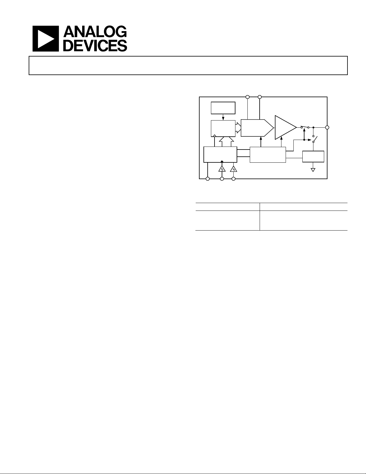
V
DD
V
OUT
GND
POWER-ON
RESET
DAC
REGISTER
8-/10-/12-BIT
DAC
INPUT
CONTROL
LOGIC
POWER-DOWN
CONTROL LOGIC
OUTPUT
BUFFER
RESISTOR
NETWORK
REF(+)
SCL SDA
ADDR
05446-001
2.7 V to 5.5 V, <100 µA, 8-/10-/12-Bit nanoDACs® with
Data Sheet
FEATURES
Single 8-, 10-, 12-bit DACs, 2 LSB INL
6-lead LFCSP and SC70 packages
Micropower operation: 100 µA max @ 5 V
Power-down to <150 nA @ 3 V
2.7 V to 5.5 V power supply
Guaranteed monotonic by design
Power-on reset to 0 V with brownout detection
3 power-down functions
2
I
C-compatible serial interface supports standard (100 kHz),
fast (400 kHz), and high speed (3.4 MHz) modes
On-chip output buffer amplifier, rail-to-rail operation
Qualified for automotive applications
APPLICATIONS
Process control
Data acquisition systems
Portable battery-powered instruments
Digital gain and offset adjustment
Programmable voltage and current sources
Programmable attenuators
GENERAL DESCRIPTION
The AD5602/AD5612/AD5622, members of the nanoDAC
family, are single 8-, 10-, 12-bit buffered voltage-out DACs that
operate from a single 2.7 V to 5.5 V supply, consuming <100 µA
at 5 V. These DACs come in tiny LFCSP and SC70 packages.
Each DAC contains an on-chip precision output amplifier that
allows rail-to-rail output swing to be achieved.
The AD5602/AD5612/AD5622 use a 2-wire I
serial interface that operates in standard (100 kHz), fast
(400 kHz), and high speed (3.4 MHz) modes.
The references for AD5602/AD5612/AD5622 are derived from
the power supply inputs to give the widest dynamic output range.
Each part incorporates a power-on reset circuit that ensures the
DAC output powers up to 0 V and remains there until a valid
write takes place to the device. The parts contain a power-down
feature that reduces the current consumption of the devices to
<150 nA at 3 V and provides software-selectable output loads
while in power-down mode. The parts are put into power-down
mode over the serial interface. The low power consumption of
the AD5602/AD5612/AD5622 in normal operation makes them
ideally suited for use in portable battery-operated equipment. The
typical power consumption is 0.4 mW at 5 V.
2
C-compatible
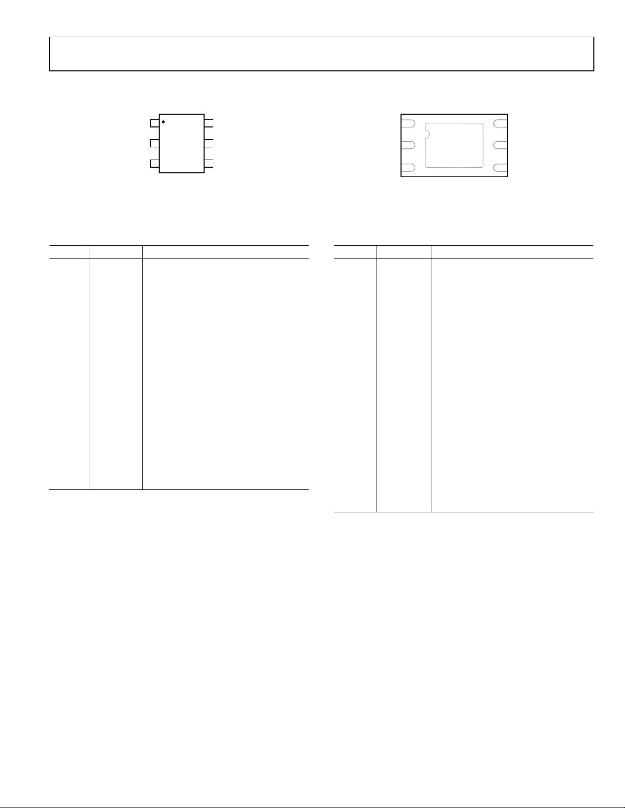
FUNCTIONAL BLOCK DIAGRAM
Figure 1.
Table 1. Related Devices
Part No. Description
AD5601/AD5611/AD5621 2.7 V to 5.5 V, <100 µA, 8-, 10-, 12-bit
nanoDAC with SPI® interface in tiny
LFCSP and SC70 packages
PRODUCT HIGHLIGHTS
1. Available in 6-lead LFCSP and SC70 packages.
2. Maximum 100 µA power consumption, single-supply
operation. These parts operate from a single 2.7 V to 5.5 V
supply, typically consuming 0.2 mW at 3 V and 0.4 mW at
5 V, making them ideal for battery-powered applications.
3. The on-chip output buffer amplifier allows the output of
the DAC to swing rail-to-rail with a typical slew rate of
0.5 V/µs.
4. Reference derived from the power supply.
5. Standard, fast, and high speed mode I
6. Designed for very low power consumption.
7. Power-down capability. When powered down, the DAC
typically consumes <150 nA at 3 V.
8. Power-on reset and brownout detection.
2
C interface.
responsibility is assumed by Analog Devices for its use, nor for any infringements of patents or other
rights of third parties that may res ult from its use. Specifications subject to chang e without notice. No
license is granted by implication or otherwise under any patent or patent rights of Analog Devices.
One Technology Way, P.O. Box 9106, Norwood, MA 02062-9106, U.S.A.
Tel: 781.329.4700
www.analog.com

AD5602/AD5612/AD5622 Data Sheet
TABLE OF CONTENTS
Features .............................................................................................. 1
Applications ....................................................................................... 1
Functional Block Diagram .............................................................. 1
General Description ......................................................................... 1
Product Highlights ........................................................................... 1
Revision History ............................................................................... 2
Specifications ..................................................................................... 3
2
I
C Timing Specifications ............................................................ 4
Timing Diagram ........................................................................... 5
Absolute Maximum Ratings ............................................................ 6
ESD Caution .................................................................................. 6
Pin Configuration and Function Descriptions ............................. 7
Typical Performance Characteristics ............................................. 8
Terminology .................................................................................... 14
Theory of Operation ...................................................................... 15
D/A Section ................................................................................. 15
Resistor String ............................................................................. 15
Output Amplifier ........................................................................ 15
Serial Interface ................................................................................ 16
Input Register .............................................................................. 16
Power-On Reset .......................................................................... 17
Power-Down Modes .................................................................. 17
Write Operation.......................................................................... 18
Read Operation........................................................................... 19
High Speed Mode ....................................................................... 20
Applications ..................................................................................... 21
Choosing a Reference as Power Supply ................................... 21
Bipolar Operation....................................................................... 21
Power Supply Bypassing and Grounding ................................ 21
Outline Dimensions ....................................................................... 22
Ordering Guide .......................................................................... 23
REVISION HISTORY
5/12—Rev. B to Rev. C
Added 6-lead LFCSP Package ........................................... Universal
Changes to Product Title ................................................................. 1
Changes to Ordering Guide .......................................................... 23
3/0
6—Rev. A to Rev. B
Changes to Table 2 ............................................................................ 3
Updates to Outline Dimensions ................................................... 22
Changes to Ordering Guide .......................................................... 23
8/05—Rev. 0 to Rev. A
Changes to Ordering Guide .......................................................... 22
6/05—Revision 0: Initial Version
Rev. C | Page 2 of 24

Data Sheet AD5602/AD5612/AD5622
AD5622
±2
LSB
B, Y versions
±6
LSB
A, W versions
1000
pF
RL = 2 kΩ
Output Noise Spectral Density
120 nV/Hz
DAC code = midscale, 10 kHz
IIN, Input Current
±1
µA
Floating-State Output Capacitance
2
pF
SPECIFICATIONS
VDD = 2.7 V to 5.5 V, RL = 2 kΩ to GND, CL = 200 pF to GND; all specifications T
Table 2.
A, B, W, Y Versions1
Parameter Min Typ Max Unit Test Conditions/Comments
STATIC PERFORMANCE DAC output unloaded
Resolution Bits
AD5602 8
AD5612 10
AD5622 12
Relative Accuracy2
AD5602 ±0.5 LSB B, Y versions
AD5612 ±0.5 LSB B, Y versions
±4 LSB A version
Differential Nonlinearity2 ±1 LSB Guaranteed monotonic by design
Zero Code Error 0.5 10 mV All 0s loaded to DAC register
Offset Error ±0.063 ±10 mV
Full-Scale Error 0.5 mV All 1s loaded to DAC register
Gain Error ±0.0004 ±0.037 % of FSR
Zero Code Error Drift 5 µV/°C
Gain Temperature Coefficient 2 ppm of FSR/°C
OUTPUT CHARACTERISTICS3
Output Voltage Range 0 VDD V
Output Voltage Settling Time 6 10 µs Code ¼ to ¾
Slew Rate 0.5 V/µs
Capacitive Load Stability 470 pF RL = ∞
MIN
to T
, unless otherwise noted.
MAX
Noise 2 DAC code = midscale, 0.1 Hz to 10 Hz
bandwidth
Digital-to-Analog Glitch Impulse 5 nV-s 1 LSB change around major carry
Digital Feedthrough 0.2 nV-s
DC Output Impedance 0.5 Ω
Short Circuit Current 15 mA VDD = 3 V/5 V
LOGIC INPUTS (SDA, SCL)
V
, Input Low Voltage 0.3 × VDD V
INL
V
, Input High Voltage 0.7 × VDD V
INH
CIN, Pin Capacitance 2 pF
V
, Input Hysteresis 0.1 × VDD V
HYST
LOGIC OUTPUTS (OPEN DRAIN)
VOL, Output Low Voltage 0.4 V I
0.6 V I
= 3 mA
SINK
= 6 mA
SINK
Floating-State Leakage Current ±1 µA
Rev. C | Page 3 of 24
AD5602/AD5612/AD5622 Data Sheet
High speed mode, CB = 400 pF
320 ns
t6
Standard mode
4 µs
t
, hold time (repeated) start condition
A, B, W, Y Versions1
Parameter Min Typ Max Unit Test Conditions/Comments
POWER REQUIREMENTS
VDD 2.7 5.5 V
IDD (Normal Mode) DAC active and excluding load current
VDD = 4.5 V to 5.5 V 75 100 µA VIH = VDD and VIL = GND
VDD = 2.7 V to 3.6 V 60 90 µA VIH = VDD and VIL = GND
IDD (All Power-Down Modes)
VDD = 4.5 V to 5.5 V 0.3 1 µA VIH = VDD and VIL = GND
VDD = 2.7 V to 3.6 V 0.15 1 µA VIH = VDD and VIL = GND
POWER EFFICIENCY
I
96 % I
OUT/IDD
1
Temperature ranges for A, B versions: −40°C to +125°C, typical at 25°C.
2
Linearity calculated using a reduced code range 64 to 4032.
3
Guaranteed by design and characterization, not production tested.
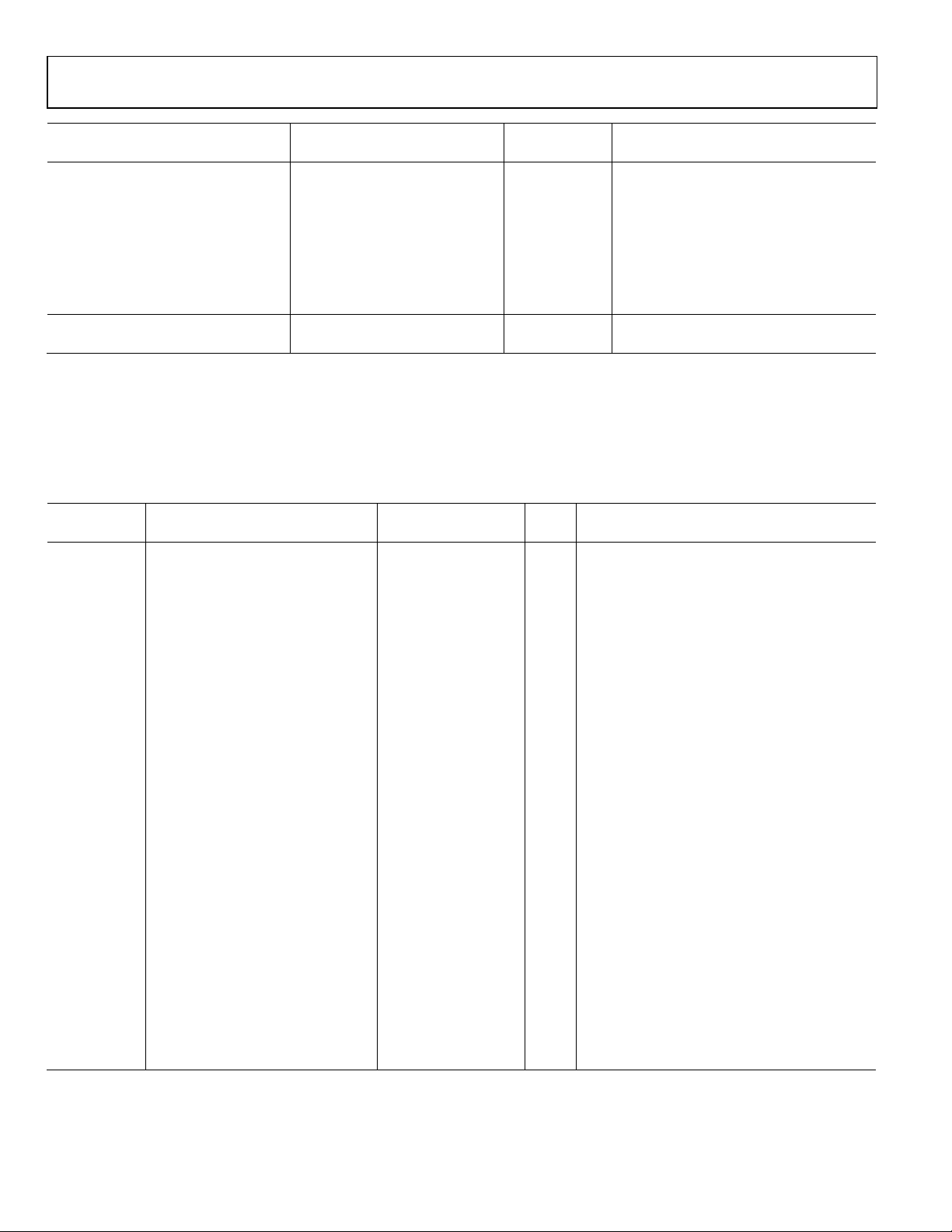
I2C TIMING SPECIFICATIONS
VDD = 2.7 V to 5.5 V; all specifications T
Table 3.
Limit at T
Parameter Conditions2 Min Max Unit Description
3
f
Standard mode 100 KHz Serial clock frequency
SCL
Fast mode 400 KHz
High speed mode, CB = 100 pF 3.4 MHz
High speed mode, CB = 400 pF 1.7 MHz
t1 Standard mode 4 µs t
Fast mode 0.6 µs
High speed mode, CB = 100 pF 60 ns
High speed mode, CB = 400 pF 120 ns
t2 Standard mode 4.7 µs t
Fast mode 1.3 µs
High speed mode, CB = 100 pF 160 ns
MIN
to T
, f
= 3.4 MHz, unless otherwise noted.1
MAX
SCL
, T
MIN
MAX
HIGH
LOW
= 2 mA, VDD = 5 V
LOAD
, SCL high time
, SCL low time
t3 Standard mode 250 ns t
Fast mode 100 ns
High speed mode 10 ns
t4 Standard mode 0 3.45 µs t
Fast mode 0 0.9 µs
High speed mode, CB = 100 pF 0 70 ns
High speed mode, CB = 400 pF 0 150 ns
t5 Standard mode 4.7 µs t
Fast mode 0.6 µs
High speed mode 160 ns
Fast mode 0.6 µs
High speed mode 160 ns
t7 Standard mode 4.7 µs t
Fast mode 1.3 µs
Rev. C | Page 4 of 24
, data setup time
SU ;D AT
, data hold time
HD ;D AT
set-up time for a repeated start condition
SU;STA,
HD ;STA
, bus free time between a stop and a start
BUF
condition
Data Sheet AD5602/AD5612/AD5622
High speed mode, CB = 400 pF
20
80
ns
High speed mode
0
10
ns
SCL
SDA
P S S P
t
8
t
6
t
5
t
3
t
10
t
9
t
4
t
6
t
1
t
7
t
2
t
11
t
12
05446-002
Limit at T
Parameter Conditions2 Min Max Unit Description
t8 Standard mode 4 µs t
Fast mode 0.6 µs
High speed mode 160 ns
t9 Standard mode 1000 ns t
Fast mode 300 ns
High speed mode, CB = 100 pF 10 80 ns
High speed mode, CB = 400 pF 20 160 ns
t10 Standard mode 300 ns t
Fast mode 300 ns
High speed mode, CB = 100 pF 10 80 ns
High speed mode, CB = 400 pF 20 160 ns
t11 Standard mode 1000 ns t
Fast mode 300 ns
High speed mode, CB = 100 pF 10 40 ns
t
Standard mode 1000 ns t
11A
Fast mode 300 ns
High speed mode, CB = 100 pF 10 80 ns
High speed mode, CB = 400 pF 20 160 ns
t12 Standard mode 300 ns t
Fast mode 300 ns
High speed mode, CB = 100 pF 10 40 ns
High speed mode, CB = 400 pF 20 80 ns
4
t
Fast mode 0 50 ns Pulse width of spike suppressed
SP
MIN
, T
MAX
, setup time for a stop condition
SU;STO
, rise time of SDA signal
RDA
, fall time of SDA signal
FDA
, rise time of SCL signal
RCL
, rise time of SCL signal after a repeated start
RCL1
condition and after an acknowledge bit
, fall time of SCL signal
FCL
1
See Figure 2. High speed mode timing specification applies to the AD5602-1/AD5612-1/AD5622-1 only. Standard and fast mode timing specifications apply to the
AD5602-1/AD5612-1/AD5622-1 and AD5602-2/AD5612-2/AD5622-2.
2
CB refers to the capacitance on the bus line.
3
The SDA and SCL timing is measured with the input filters enabled. Switching off the input filters improves the transfer rate but has a negative effect on EMC behavior
of the part.
4
Input filtering on the SCL and SDA inputs suppress noise spikes that are less than 50 ns for fast mode or 10 ns for high speed mode.
TIMING DIAGRAM
Figure 2. 2-Wire Serial Interface Timing Diagram
Rev. C | Page 5 of 24
AD5602/AD5612/AD5622 Data Sheet
human body and test equipment and can discharge without detection. Although this product features
electrostatic discharges. Therefore, proper ESD precautions are recommended to avoid performance
ABSOLUTE MAXIMUM RATINGS
TA = 25°C, unless otherwise noted.
Table 4.
Parameter Rating
VDD to GND –0.3 V to + 7.0 V
Digital Input Voltage to GND –0.3 V to VDD + 0.3 V
V
to GND –0.3 V to VDD + 0.3 V
OUT
Operating Temperature Range
Extended Automotive (W, Y Versions) –40°C to +125°C
Extended Industrial (A, B Versions)
Storage Temperature Range –65°C to +160°C
Maximum Junction Temperature 150°C
SC70 Package
θJA Thermal Impedance 332°C/W
θJC Thermal Impedance 120°C/W
LFCSP Package
θJA Thermal Impedance 95°C/W
Lead Temperature, Soldering
Vapor Phase (60 sec) 215°C
Infrared (15 sec) 220°C
ESD 2.0 kV
−40°C to +85°C
Stresses above those listed under Absolute Maximum Ratings
may cause permanent damage to the device. This is a stress
rating only; functional operation of the device at these or any
other conditions above those indicated in the operational
section of this specification is not implied. Exposure to absolute
maximum rating conditions for extended periods may affect
device reliability.
ESD CAUTION
ESD (electrostatic discharge) sensitive device. Electrostatic charges as high as 4000 V readily accumulate on
the
proprietary ESD protection circuitry, permanent damage may occur on devices subjected to high energy
degradation or loss of functionality.
Rev. C | Page 6 of 24
Data Sheet AD5602/AD5612/AD5622
ADDR
1
SCL
2
SDA
3
V
OUT
6
GND
5
V
DD
4
AD5602/
AD5612/
AD5622
TOP VIEW
(Not to Scale)
05446-003
AD5602/
AD5612/
A
D5622
TOP VIEW
(Not to S cale)
05446-051
3V
OUT
1ADDR
2GND
4 V
DD
6 SDA
5 SCL
NOTES
1. THE EXP OSED PAD SHOULD BE CONNECTED
TO GRO UND ( GND).
PIN CONFIGURATION AND FUNCTION DESCRIPTIONS
Figure 3. SC70 Pin Configuration
Table 5. SC79 Pin Function Descriptions
Pin N o. Mnemonic Description
1 ADDR Three-State Address Input. Sets the two
least significant bits (Bit A1, Bit A0) of
the 7-bit slave address (see Table 7).
2 SCL Serial Clock Line. This is used in
conjunction with the SDA line to clock
data into or out of the 16-bit input
register.
3 SDA Serial Data Line. This is used in
conjunction with the SCL line to clock
data into or out of the 16-bit input
register. It is a bidirectional, open-drain
data line that should be pulled to the
supply with an external pull-up resistor.
4 VDD Power Supply Input. These parts can be
operated from 2.7 V to 5.5 V, and VDD
should be decoupled to GND.
5 GND Ground. The ground reference point for
all circuitry on the part.
6 V
Analog Output Voltage from the DAC.
OUT
The output amplifier has rail-to-rail
operation.
Figure 4. LFCSP Pin Configuration
Table 6. LFCSP Pin Function Descriptions
Pin No. Mnemonic Description
1 ADDR Three-State Address Input. Sets the
two least significant bits (Bit A1, Bit A0)
of the 7-bit slave address (see Table 7).
2 GND Ground. The ground reference point for
all circuitry on the part.
3 V
Analog Output Voltage from the DAC.
OUT
The output amplifier has rail-to-rail
operation.
4 VDD Power Supply Input. These parts can be
operated from 2.7 V to 5.5 V, and VDD
should be decoupled to GND.
5 SCL Serial Clock Line. This is used in
conjunction with the SDA line to clock
data into or out of the 16-bit input
register.
6 SDA Serial Data Line. This is used in
conjunction with the SCL line to clock
data into or out of the 16-bit input
register. It is a bidirectional, open-drain
data line that should be pulled to the
supply with an external pull-up resistor.
EPAD Exposed Pad. The exposed pad should
be connected to ground (GND).
Rev. C | Page 7 of 24
AD5602/AD5612/AD5622 Data Sheet
DAC CODE
INL ERROR ( LSB)
1.0
0.8
0.6
0.4
0.2
0
–1.0
–0.8
–0.6
–0.4
–0.2
0 1000500 20001500 350030002500 4000
V
DD
= 5V
T
A
= 25°C
05446-004
DAC CODE
DNL ERROR (L S B)
0.15
0
–0.20
–0.15
–0.10
0.10
–0.05
0.05
0 1000500 20001500 350030002500 4000
VDD= 5V
T
A
= 25°C
05446-005
DAC CODE
INL ERROR ( LSB)
0.25
0.20
0.15
0.10
0.05
0
–0.25
–0.20
–0.15
–0.10
–0.05
0 400200 600 800 1000
VDD= 5V
T
A
= 25°C
05446-047
DAC CODE
DNL ERROR (L S B)
0.05
0.04
0.03
0.02
0.01
0
–0.05
–0.04
–0.03
–0.02
–0.01
0 400200 600 800 1000
VDD= 5V
T
A
= 25°C
05446-048
DAC CODE
INL ERROR ( LSB)
0.06
0.04
0.02
0
–0.06
–0.04
–0.02
0 10050 150 200 250
VDD= 5V
T
A
= 25°C
05446-049
DAC CODE
DNL ERROR (L S B)
0.015
0.010
0.005
0
–0.015
–0.005
–0.010
0 10050 150 200 250
V
DD
= 5V
T
A
= 25°C
05446-050
TYPICAL PERFORMANCE CHARACTERISTICS
Figure 5. Typical AD5622 Integral Nonlinearity Error
Figure 6. Typical AD5622 Differential Nonlinearity Error
Figure 8. Typical AD5612 Differential Nonlinearity Error
Figure 9. Typical AD5602 Integral Nonlinearity Error
Figure 7. Typical AD5612 Integral Nonlinearity Error
Figure 10. Typical AD5602 Differential Nonlinearity Error
Rev. C | Page 8 of 24

Data Sheet AD5602/AD5612/AD5622
DAC CODE
TUE (LSB)
1
0
–7
–6
–5
–4
–3
–2
–1
0 1000500 20001500 350030002500 4000
V
DD
= 5V
T
A
= 25°C
05446-006
V
DD
(V)
INL ERROR ( LSB)
0.8
0.6
–0.8
–0.6
–0.4
–0.2
0
0.2
0.4
2.7 3.2 4.23.7 5.24
.7
T
A
= 25°C
MAX INL
MIN INL
05446-007
VDD(V)
TUE (LSB)
0
–8
–7
–6
–5
–4
–3
–2
–1
2.7 3.2 4.23.7 5.24.7
TA= 25°C
MAX TUE
MIN TUE
05446-008
V
DD
(V)
DNL ERROR (L S B)
0.5
0.4
0.3
0.2
0.1
0
–0.3
–0.2
–0.1
2.7 3.2 4.23.7 5.24.7
TA= 25°C
MAX DNL
MIN DNL
05446-009
TEMPERATURE (°C)
INL ERROR ( LSB)
0.5
0.4
0.3
0.2
0.1
0
–0.3
–0.2
–0
.1
–40 0–20 604020 12010080
MAX INL = 5V
MAX INL = 3V
MIN INL = 5V
MIN INL = 3V
05446-010
TEMPERATURE (°C)
TUE (LSB)
8
7
6
5
4
3
0
1
2
–40 0–20 604020 12010080
MAX TUE = 5V
MAX TUE = 3V
MIN TUE = 5V
MIN TUE = 3V
05446-011
Figure 11. Typical AD5622 Total Unadjusted Error
Figure 12. AD5622 INL Error vs. Supply
Figure 14. AD5622 DNL Error vs. Supply
Figure 15. AD5622 INL Error vs. Temperature (3 V/5 V Supply)
Figure 13. AD5622 Total Unadjusted Error vs. Supply
Figure 16. AD5622 Total Unadjusted Error vs. Temperature (3 V/5 V Supply)
Rev. C | Page 9 of 24

AD5602/AD5612/AD5622 Data Sheet
TEMPERATURE (°C)
DNL ERROR (L S B)
0.6
0.5
0.4
0.3
0.2
0.1
0
–0.3
–0.2
–0.1
–40 0–20 604020 12010080
MAX DNL = 5V
MAX DNL = 3V
MIN DNL = 5V
MIN DNL = 3V
05446-012
TEMPERATURE (°C)
ERROR (mV)
4
0
2
–2
–4
–8
–10
–6
–40 –20 0 604020 100 12080
ZERO CODE ERROR = 3V
FULL-SCALE ERROR = 3V
FULL-SCALE ERROR = 5V
ZERO CODE ERROR = 5V
05446-013
VDD(V)
ERROR (mV)
1
0
–1
–2
–3
–4
–5
–8
–7
–6
2.7 3.2 4.23.7 5.24.7
ZERO CODE ERROR
TA= 25°C
FULL-SCALE ERROR
05446-014
TEMPERATURE (°C)
ERROR (mV)
1.8
1.6
1.4
1.2
1.0
0.8
0.6
0
0.2
0.4
–40 0–20 604020 12010080
OFFSET ERROR = 5V
OFFSET ERROR = 3V
05446-015
TEMPERATURE (°C)
ERROR (%FSR)
0.00025
0.00020
0.00015
0.00010
0
0.00005
–40 0–20 604020 12010080
GAIN ERROR = 5V
GAIN ERROR = 3V
05446-016
0
0.02
0.03
0.04
0.05
0.06
0.07
0.08
0.
09
0.10
2.7 3.2 3.7 4.2 4.7 5.2
V
DD
(V)
I
DD
(µA)
T
A
= 25°C
0.01
05446-017
Figure 17. AD5622 DNL Error vs. Temperature (3 V/5 V Supply)
Figure 18. Zero Code/Full-Scale Error vs. Temperature (3 V/5 V Supply)
Figure 20. Offset Error vs. Temperature (3 V/5 V Supply)
Figure 21. Gain Error vs. Temperature ( 3 V/5 V Supply)
Figure 19. Zero Code/Full-Scale Error vs. Supply Voltage
Figure 22. Supply Current vs. Supply Voltage
Rev. C | Page 10 of 24

Data Sheet AD5602/AD5612/AD5622
0
0.01
0.02
0.03
0.04
0.05
0.06
0.07
0.08
0.09
0.10
–40 –20 0 20 40 60 80 100 120 140
TEMPERATURE (°C)
I
DD
(µA)
V
DD
= 3V
V
DD
= 5V
05446-018
0
10
20
30
40
50
60
70
0 2000 4000 6000 8000 10000 12000 14000 16000
DAC CODE
I
DD
(µA)
V
DD
= 5V
V
DD
= 3V
T
A
= 25°C
05446-019
V
LOGIC
(V)
I
DD
(µA)
900
800
700
600
500
400
0
100
200
300
0 0.5 1.0 2.52.01.5 5.04.54.03.53.0
SCL/SDA DECREASING
V
DD
= 5V
SCL/SDA DECREASING
V
DD
= 3V
SCL/SDA
INCREASING
V
DD
= 3V
SCL/SDA INCREASING
V
DD
= 5V
05446-020
0
2
4
6
8
10
12
0.05456
0.05527
0.05599
0.05671
0.05742
0.05814
0.05885
0.06648
0.06710
0.06773
0.06835
0.06897
0.06960
0.07022
0.07084
0.07147
0.07209
0.07271
0.07334
IDD(µA)
FREQUENCY
VDD= 5V
V
IH
= V
DD
VIL= GND
T
A
= 25°C
V
DD
= 3V
V
IH
= V
DD
VIL= GND
T
A
= 25°C
05446-021
–0.6
–0.4
–0.2
0.0
0.2
0.4
0.6
0.8
–15 –10 –5 0 5 10 15
I (mA)
ΔV
O
(V)
DAC LOADED WITH ZERO-SCALE CODE
V
DD
= 5V
T
A
= 25°C
DAC LOADED WITH FULL-SCALE CODE
05446-037
CH2
CH1
VDD= 5V
T
A
= 25°C
V
DD
V
OUT
= 70mV
CH1 = 1V/DIV, CH2 = 20mV/DIV, TIME BASE = 20µs/DIV
05446-038
Figure 23. Supply Current vs. Temperature (3 V/5 V Supply)
Figure 24. Supply Current vs. Digital Input Code
Figure 26. I
Histogram (3 V/5 V Supply)
DD
Figure 27. Sink and Source Capability
Figure 25. Supply Current vs. SCL/SDA Logic Voltage
Figure 28. Power-On Reset to 0 V
Rev. C | Page 11 of 24

AD5602/AD5612/AD5622 Data Sheet
CH1 = 5V/DIV, CH2 = 1V/DIV, TIME BASE = 2µs/DIV
CH1
CH2
VDD= 5V
T
A
= 25°C
05446-039
CH1 = 5V/DIV, CH2 = 1V/DIV, TIME BASE = 2µs/DIV
CH1
CH2
VDD= 5V
T
A
= 25°C
05446-040
CH1 = 5V/DIV, CH2 = 1V/DIV, TIME BASE = 2µs/DIV
CH1
CH2
V
DD
= 5V
T
A
= 25°C
05446-041
CH1 = 1V/DIV, CH2 = 3V/DIV, TIME BASE = 50µs/DIV
CH2
CH1
V
DD
V
OUT
V
DD
= 5V
T
A
= 25°C
05446-042
SAMPLE NUMBER
AMPLITUDE (V)
0 100 200 300 400 500
2.458
2.456
2.454
2.452
2.450
2.448
2.446
2.444
2.442
2.440
2.438
2.436
V
DD
= 5V
T
A
= 25°C
LOAD = 2kΩ AND 220pF
CODE 0x800 TO 0x7FF
10ns/SAMPLE NUMBER
05446-043
SAMPLE NUMBER
AMPLITUDE (V)
2.4278
2.4276
2.4274
2.4272
2.4270
2.4268
2.4266
2.4264
2.4262
2.4260
0 200100 300 400 500
V
DD
= 5V
T
A
= 25°C
LOAD = 2kΩ AND 220pF
10ns/SAMPLE NUMBER
05446-044
Figure 29. Exiting Power-Down Mode
Figure 30. Full-Scale Settling Time
Figure 32. V
OUT
vs. VDD
Figure 33. Digital-to-Analog Glitch Impulse
Figure 31. Half-Scale Settling Time
Figure 34. Digital Feedthrough
Rev. C | Page 12 of 24

Data Sheet AD5602/AD5612/AD5622
CH1
V
DD
= 5V
T
A
= 25°C
MIDSCALE LOADED
CH1 = 5µV/DIV
05446-045
0
100
200
300
400
500
600
700
100 1000 10000 100000
FREQUENCY (Hz)
OUTPUT NOISE SPECTRAL DENSITY (nV/ Hz)
FULL SCALE
ZERO SCALE
V
DD
= 5V
T
A
= 25°C
UNLOADED OUTPUT
MIDSCALE
05446-046
Figure 35. 1/f Noise, 0.1 Hz to 10 Hz Bandwidth
Figure 36. Output Noise Spectral Density
Rev. C | Page 13 of 24

AD5602/AD5612/AD5622 Data Sheet
TERMINOLOGY
Relative Accuracy
For the DAC, relative accuracy or integral nonlinearity (INL) is
a measure of the maximum deviation, in LSBs, from a straight
line passing through the endpoints of the DAC transfer
function. A typical INL vs. code plot can be seen in Figure 5.
Differential Nonlinearity (DNL)
Differential nonlinearity is the difference between the measured
change and the ideal 1 LSB change between any two adjacent
codes. A specified differential nonlinearity of ±1 LSB maximum
ensures monotonicity. This DAC is guaranteed monotonic by
design. A typical DNL vs. code plot can be seen in Figure 6.
Zero Code Error
Zero-code error is due to a combination of the offset errors in
the DAC and output amplifier; it is a measure of the output
error when zero code (0x0000) is loaded to the DAC register.
Ideally, the output should be 0 V. The zero-code error is always
positive in the AD5602/AD5612/AD5622 because the output of
the DAC cannot go below 0 V. Zero-code error is expressed in
m V. A plot of zero-code error vs. temperature can be seen in
Figure 18.
Full-Scale Error
Full-scale error is a measure of the output error when full-scale
code (0xFFFF) is loaded to the DAC register; it is expressed in
percent of full-scale range. Ideally, the output should be V
1 LSB. A plot of full-scale error vs. temperature can be seen in
Figure 18.
–
DD
Gain Error
Gain error is a measure of the span error of the DAC. It is the
deviation in slope of the DAC transfer characteristic from ideal
expressed as a percent of the full-scale range.
Total Unadjusted Error (TUE)
Total unadjusted error is a measure of the output error taking
all the various errors into account. A typical TUE vs. code plot
can be seen in Figure 11.
Zero Code Error Drift
Zero code error drift is a measure of the change in zero code
error with a change in temperature. It is expressed in µV/°C.
Gain Error Drift
Gain error drift is a measure of the change in gain error with
changes in temperature. It is expressed in (ppm of full-scale
range)/°C.
Digital-to-Analog Glitch Impulse
Digital-to-analog glitch impulse is the impulse injected into the
analog output when the input code in the DAC register changes
state. It is normally specified as the area of the glitch in nV-s and
is measured when the digital input code is changed by 1 LSB at
the major carry transition (0x7FFF to 0x8000) (see Figure 33).
Digital Feedthrough
Digital feedthrough is a measure of the impulse injected into
the analog output of the DAC from the digital inputs of the DAC,
but is measured when the DAC output is not updated. It is
specified in nV-s and measured with a full-scale code change on
the data bus, that is, from all 0s to all 1s, and vice versa
(see Figure 34).
Rev. C | Page 14 of 24

Data Sheet AD5602/AD5612/AD5622
V
DD
V
OUT
GND
RESISTOR
NETWORK
REF (+)
REF (–)
OUTPUT
AMPLIFIER
DAC REGISTER
05446-022
×=
n
DDOUT
D
VV
2
R
R
R
R
R
TO OUTPUT
AMPLIFIER
05446-023
THEORY OF OPERATION
D/A SECTION
The AD5602/AD5612/AD5622 DACs are fabricated on a
CMOS process. The architecture consists of a string DACs
followed by an output buffer amplifier. Figure 37 shows a block
diagram of the DAC architecture.
tapped off by closing one of the switches connecting the string
to the amplifier. Because it is a string of resistors, it is
guaranteed monotonic.
Figure 37. DAC Architecture
Since the input coding to the DAC is straight binary, the ideal
output voltage is given by
where:
D is the decimal equivalent of the binary code that is loaded
to the DAC register; it can range from 0 to 255 (AD5602),
0 to 1023 (AD5612), or 0 to 4095 (AD5622).
n is the bit resolution of the DAC.
RESISTOR STRING
The resistor string structure is shown in Figure 38. It is simply a
string of resistors, each of value R. The code loaded to the DAC
register determines at which node on the string the voltage is
tapped off to be fed into the output amplifier. The voltage is
Figure 38. Resistor String Structure
OUTPUT AMPLIFIER
The output buffer amplifier is capable of generating rail-to-rail
voltages on its output, giving an output range of 0 V to V
capable of driving a load of 2 kΩ in parallel with 1000 pF to
GND. The source and sink capabilities of the output amplifier
can be seen in Figure 27. The slew rate is 0.5 V/µs with a halfscale settling time of 5 µs with the output unloaded.
DD
. It is
Rev. C | Page 15 of 24

AD5602/AD5612/AD5622 Data Sheet
VDD 0 0
DATA
BITS
DB15 (MSB) DB0 (LSB)
0 0 PD1 PD0 D7 D6 D5 D4 D3 D2 D1 D0 X X X X
05446-024
DATA BITS
DB15 (MSB) DB0 (LSB)
0 0 PD1 PD0 D9 D8 D7 D6 D5 D4 D3 D2 D1 D0 X X
05446-025
DATA BITS
DB15 (MSB) DB0 (LSB)
0 0 PD1 PD0 D11 D10 D9 D8 D7 D6 D5 D4 D3 D2 D1 D0
05446-026
SERIAL INTERFACE
The AD5602/AD5612/AD5622 have 2-wire I2C-compatible
serial interfaces (refer to I
2
C-Bus Specification, Version 2.1,
January 2000, available from Philips Semiconductor). The
AD5602/AD5612/AD5622 can be connected to an I
2
C bus as a
slave device, under the control of a master device. See Figure 2
for a timing diagram of a typical write sequence.
The AD5602/AD5612/AD5622 support standard (100 kHz),
fast (400 kHz), and high speed (3.4 MHz) data transfer modes.
Support is not provided for 10-bit addressing and general call
addressing.
The AD5602/AD5612/AD5622 each have a 7-bit slave address.
The five MSBs are 00011 and the two LSBs are determined by
the state of the ADDR pin. The facility to make hardwired
changes to ADDR allows the user to incorporate up to three of
these devices on one bus as outlined in Table 7.
The 2-wire serial bus protocol operates as follows:
1. The master initiates data transfer by establishing a start
condition, which is when a high-to-low transition on the
SDA line occurs while SCL is high. The following byte is
the address byte, which consists of the 7-bit slave address.
The slave address corresponding to the transmitted address
responds by pulling SDA low during the ninth clock pulse
(this is termed the acknowledge bit). At this stage, all other
devices on the bus remain idle while the selected device
waits for data to be written to, or read from, its shift register.
2. Data is transmitted over the serial bus in sequences of nine
clock pulses (eight data bits followed by an acknowledge
bit). The transitions on the SDA line must occur during the
low period of SCL and remain stable during the high
period of SCL.
3. When all data bits have been read or written, a stop
condition is established. In write mode, the master pulls
the SDA line high during the 10th clock pulse to establish a
stop condition. In read mode, the master issues a no
acknowledge for the ninth clock pulse (that is, the SDA line
remains high). The master then brings the SDA line low
before the 10th clock pulse, and then high during the 10th
clock pulse to establish a stop condition.
Table 7. Device Address Selection
ADDR A1 A0
GND 1 1
NC (No Connection) 1 0
INPUT REGISTER
The input register is 16 bits wide. Figure 39, Figure 40, and
Figure 41 illustrate the contents of the input register for each
part. Data is loaded into the device as a 16-bit word under the
control of a serial clock input, SCL. The timing diagram for this
operation is shown in Figure 2. The 16-bit word consists of four
control bits followed by 8, 10, or 12 bits of data, depending on
the device type. MSB (DB15) is loaded first. The first two bits
are reserved bits that must be set to zero, the next two bits are
control bits that select the mode of operation of the device
(normal mode or any one of three power-down modes). See the
Power-Down Modes section for a complete description. The
remaining bits are left-justified DAC data bits, starting with the
MSB and ending with the LSB.
Figure 39. AD5602 Input Register Contents
Figure 40. AD5612 Input Register Contents
Figure 41. AD5622 Input Register Contents
Rev. C | Page 16 of 24

Data Sheet AD5602/AD5612/AD5622
POWER-DOWN
CIRCUITRY
RES
ISTOR
NETWORK
V
OUT
RESISTOR
STRING DAC
AMPLIFIER
05446-027
POWER-ON RESET
The AD5602/AD5612/AD5622 each contain a power-on reset
circuit that controls the output voltage during power-up. The
DAC register is filled with zeros and the output voltage is 0 V
where it remains until a valid write sequence is made to the
DAC. This is useful in applications where it is important to
know the state of the DAC output while it is in the process of
powering up.
POWER-DOWN MODES
The AD5602/AD5612/AD5622 each contain four separate
modes of operation. These modes are software-programmable
by setting Bit PD1 and Bit PD0 in the control register. Table 8
shows how the state of the bits corresponds to the mode of
operation of the device.
Table 8. Modes of Operation
PD1 PD0 Operating Mode
0 0 Normal operation
0 1 Power-down (1 kΩ load to GND)
1 0 Power-down (100 kΩ load to GND)
1 1 Power-down (Three-state output)
When both bits are set to 0, the part works normally with its
usual power consumption of 100 µA maximum at 5 V. However,
for the three power-down modes, the supply current falls to
<150 nA (at 3 V). Not only does the supply current fall, but the
output stage is internally switched from the output of the
amplifier to a resistor network of known values. This gives the
advantage of knowing the output impedance of the part while
the part is in power-down mode. There are three different
options. The output is connected internally to GND through a
1 kΩ resistor, a 100 kΩ resistor, or it is left open-circuited
(three-state). Figure 42 shows the output stage.
Figure 42. Output Stage During Power-Down
The bias generator, output amplifier, resistor string, and other
associated linear circuitry are all shut down when the powerdown mode is activated. However, the contents of the DAC
register are unaffected when in power-down. The time to exit
power-down is typically 14 µs for V
= 5 V and 17 µs for VDD =
DD
3 V (see Figure 29).
Rev. C | Page 17 of 24

AD5602/AD5612/AD5622 Data Sheet
SCL
SDA
START BY
MASTER
ACK. BY
AD5602
ACK. BY
AD5602
ACK. BY
AD5602
STOP BY
MASTER
FRAME 2
MOST SIGNIFICANT DATA BYTE
FRAME 1
SERIAL BUS ADDRESS BYTE
0
1 9
1
9 9
91
0 0 1 1 A1 A0 R/W 0 0 PD1 PD0 D7 D6 D5 D4
D3 D2 D1 D0 X X X X
SCL (CONTINUED)
SDA (CONTINUED)
FRAME 3
LEAST SIGNIFICANT DATA BYTE
05446-028
SCL
SDA
START BY
MASTER
ACK. BY
AD5612
ACK. BY
AD5612
ACK. BY
AD5612
STOP BY
MASTER
FRAME 2
MOST SIGNIFICANT DATA BYTE
FRAME 1
SERIAL BUS ADDRESS BYTE
0
1 9
1
9 9
91
0 0 1 1 A1 A0 R/W 0 0 PD1 PD0 D9 D8 D7 D6
D5 D4 D3 D2 D1 D0 X X
SCL (CONTINUED)
SDA (CONTINUED)
FRAME 3
LEAST SIGNIFICANT DATA BYTE
05446-029
SCL
SDA
START BY
MASTER
ACK. BY
AD5622
ACK. BY
AD5622
ACK. BY
AD5622
STOP BY
MASTER
FRAME 2
MOST SIGNIFICANT DATA BYTE
FRAME 1
SERIAL BUS ADDRESS BYTE
0
1 9
1
9 9
91
0 0 1 1 A1 A0 R/W 0 0 PD1 PD0 D11 D10 D9 D8
D7 D6 D5 D4 D3 D2 D1 D0
SCL (CONTINUED)
SDA (CONTINUED)
FRAME 3
LEAST SIGNIFICANT DATA BYTE
05446-030
WRITE OPERATION
When writing to the AD5602/AD5612/AD5622, the user must
begin with a start command followed by an address byte (R/
0), after which the DAC acknowledges that it is prepared to
receive data by pulling SDA low.
W
=
Two bytes of data are then written to the DAC, the most
significant byte followed by the least significant byte as shown in
Figure 40; both of these data bytes are acknowledged by the
AD5602/AD5612/AD5622. A stop condition follows. The write
operations for the three DACs are shown in Figure 43, Figure 44,
and Figure 45.
Figure 43. AD5602 Write Sequence
Figure 44. AD5612 Write Sequence
Figure 45. AD5622 Write Sequence
Rev. C | Page 18 of 24

Data Sheet AD5602/AD5612/AD5622
SCL
SDA
START BY
MASTER
ACK. BY
AD5602
ACK. BY
MASTER
NO ACK. BY
MASTER
STOP BY
MASTER
FRAME 2
MOST SIGNIFICANT DATA BYTE FROM AD5602
FRAME 1
SERIAL BUS ADDRESS BYTE
0
1 9
1 9
91
0 0 1 1 A1 A0 R/W PD1 PD0 D7 D6 D5 D4 D3 D2
D1 D0 0 0 0 0 0 0
SCL (CONTINUED)
SDA (CONTINUED)
FRAME 3
LEAST SIGNIFICANT DATA BYTE FROM AD5602
05446-031
SCL
SDA
START BY
MASTER
ACK. BY
AD5612
ACK. BY
MASTER
NO ACK. BY
MASTER
STOP BY
MASTER
FRAME 2
MOST SIGNIFICANT DATA BYTE FROM AD5612
FRAME 1
SERIAL BUS ADDRESS BYTE
0
1 9
1 9
91
0 0 1 1 A1 A0 R/W PD1 PD0 D9 D8 D7 D6 D5 D4
D3 D2 D1 D0 0 0
0 0
SCL (CONTINUED)
SDA (CONTINUED)
FRAME 3
LEAST SIGNIFICANT DATA BYTE FROM AD5612
05446-032
SCL
SDA
START BY
MASTER
ACK. BY
AD5622
ACK. BY
MASTER
NO ACK. BY
MASTER
STOP BY
MASTER
FRAME 2
MOST SIGNIFICANT DATA BYTE FROM AD5622
FRAME 1
SERIAL BUS ADDRESS BYTE
0
1 9
1 9
91
0 0 1 1 A1 A0 R/W PD1 PD0 D11 D10 D9 D8 D7 D6
D5 D4 D3 D2 D1 D0
0 0
SCL (CONTINUED)
SDA (CONTINUED)
FRAME 3
LEAST SIGNIFICANT DATA BYTE FROM AD5622
05446-033
READ OPERATION
When reading data back from the AD5602/AD5612/AD5622,
the user begins with a start command followed by an address
byte (R/
= 1), after which the DAC acknowledges that it is
W
prepared to transmit data by pulling SDA low. Two bytes of data
are then read from the DAC, which are both acknowledged by
the master as shown in Figure 46, Figure 47, and Figure 48. A
stop condition follows.
Figure 46. AD5602 Read Sequence
Figure 47. AD5612 Read Sequence
Figure 48. AD5622 Read Sequence
Rev. C | Page 19 of 24

AD5602/AD5612/AD5622 Data Sheet
1 9
91
0 0 0 0 1 X X X 0 0 0 1 1 A1 A0
START BY
MASTER
ACK. BY
AD56x2
NACK. SR
SERIAL BUS ADDR
ESS BYTEHS-MODE MASTER CODE
HIGH-SPEED MODE
FAST M
ODE
SCL
SDA
R/W
05446-034
HIGH SPEED MODE
High speed mode communication commences after the master
addresses all devices connected to the bus with the Master
Code 00001XXX to indicate that a high speed mode transfer is
to begin. No device connected to the bus is permitted to
acknowledge the high speed master code, therefore, the code is
followed by a no acknowledge. The master must then issue a
repeated start followed by the device address. The selected
device then acknowledges its address. All devices continue to
operate in high speed mode until the master issues a stop
condition. When the stop condition is issued, the devices return
to standard/fast mode.
Figure 49. Placing the AD5602/AD5612/AD5622 into High Speed Mode
Rev. C | Page 20 of 24

Data Sheet AD5602/AD5612/AD5622
AD5602/
AD5612/
AD5622
SCL
SDA
7V
5V
V
OUT
= 0V TO 5V
ADR425
05446-035
ADR395
±6
25
5
×−
+
×
×=
R1
R2
V
R1
R2R1D
VV
DD
n
DDO
2
V5
2
10
−
×
=
n
O
D
V
+5V
–5V
AD820/
OP295
+5V
AD5602/
AD5612/
AD5622
10µF
0.1µF
V
DD
V
OUT
R1
10kΩ
SDA SCL
R2
10kΩ
±5V OUT
05446-036
APPLICATIONS
CHOOSING A REFERENCE AS POWER SUPPLY
The AD5602/AD5612/AD5622 come in tiny LFCSP and SC70
packages with less than 100 µA supply current, thereby making
the choice of reference dependent upon the application
requirement. For space-saving applications, the ADR425 is
available in an SC70 package with excellent drift at 3ppm/°C. It
also provides very good noise performance at 3.4 µV p-p in the
0.1 Hz to 10 Hz range.
Because the supply current required by the AD5602/AD5612/
AD5622 DACs is extremely low, they are ideal for low supply
applications. The ADR293 voltage reference is recommended in
this case. This requires 15 µA of quiescent current and can
therefore drive multiple DACs in the one system, if required.
With V
This is an output voltage range of ±5 V with 0x000 corresponding
to a −5 V output, and 0xFFF corresponding to a +5 V output.
= 5 V, R1 = R2 = 10 kΩ
DD
Figure 51. Bipolar Operation with the AD5602/AD5612/AD5622
POWER SUPPLY BYPASSING AND GROUNDING
When accuracy is important in a circuit, it is helpful to carefully
consider the power supply and ground return layout on the
board. The printed circuit board containing the AD5602/
Figure 50. ADR425 as Power Supply
Examples of some recommended precision references for use as
supplies to the AD5602/AD5612/AD5622 are shown in Table 9.
Table 9. Recommended Precision References
Part
No.
Initial
Accuracy
(mV max)
Temper ature
Drift
(ppm/°C max)
0.1 Hz to 10 Hz Noise
(µV p-p typ)
ADR435 ±6 3 3.4
ADR425 ±6 3 3.4
ADR02 ±5 3 15
BIPOLAR OPERATION
The AD5602/AD5612/AD5622 have been designed for singlesupply operation, but a bipolar output range is also possible
using the circuit in Figure 51. The circuit in Figure 51 gives an
output voltage range of ±5 V. Rail-to-rail operation at the
amplifier output is achievable using an AD820 or an OP295 as
the output amplifier.
The output voltage for any input code can be calculated as
where:
D represents the input code in decimal.
n represents the bit resolution of the DAC.
Rev. C | Page 21 of 24
AD5612/AD5622 should have separate analog and digital
sections, each having its own area of the board. If the AD5602,
AD5612, or AD5622 is in a system where other devices require
an AGND to DGND connection, the connection should be
made at one point only. This ground point should be as close as
possible to the AD5602/AD5612/AD5622.
The power supply to the AD5602/AD5612/AD5622 should be
bypassed with 10 µF and 0.1 µF capacitors. The capacitors
should be physically as close as possible to the device with the
0.1 µF capacitor ideally right up against the device. The 10 µF
capacitors are the tantalum bead type. It is important that the
0.1 µF capacitor has low effective series resistance (ESR) and
effective series inductance (ESI), such as common ceramic
types. This 0.1 µF capacitor provides a low impedance path to
ground for high frequencies caused by transient currents due to
internal logic switching.
The power supply line should have as large a trace as possible to
provide a low impedance path and reduce glitch effects on the
supply line. Clocks and other fast switching digital signals
should be shielded from other parts of the board by digital
ground. Avoid crossover of digital and analog signals if possible.
When traces cross on opposite sides of the board, ensure that
they run at right angles to each other to reduce feedthrough
effects through the board. The best board layout technique is
the microstrip technique where the component side of the
board is dedicated to the ground plane only and the signal
traces are placed on the solder side. However, the microstrip
technique is not always possible with a 2-layer board.

AD5602/AD5612/AD5622 Data Sheet
1.30BSC
C
OMPLIANT TO JEDEC STANDARDS MO-203-AB
1.
00
0.90
0.70
0.46
0.36
0.26
2.20
2.00
1.80
2.40
2.10
1.80
1.35
1.25
1.15
072809-A
0.10 MAX
1.10
0.80
0.40
0.10
0.22
0.08
3
1 2
46
5
0.65BSC
COPLANARITY
0.10
SEATING
PLANE
0.30
0.15
1.50
1.40
1.30
0.45
0.40
0.35
TOP VIEW
6
1
4
3
BOTTOM VIEW
PIN 1 INDEX
AREA
SEATING
PLANE
0.80
0.75
0.70
1.70
1.60
1.50
0.203 REF
0.05 MAX
0.00 MIN
0.65 REF
EXPOSED
PAD
PIN 1
INDICATOR
(R 0.15)
FOR PROP E R CONNECTION O F
THE EXPOSED PAD, REFER TO
THE PIN CO NFIGURATION AND
FUNCTIO N DE S CRIPTIONS
SECTION OF THIS DATA SHEET.
03-29-2012-B
2.10
2.00
1.90
3.10
3.00
2.90
COMPLIANTTOJEDEC STANDARDS MO-229
COPLANARITY
0.08
0.20 MIN
0.35
0.30
0.25
OUTLINE DIMENSIONS
Figure 52. 6-Lead Thin Shrink Small Outline Transistor Package [SC70]
(KS-6)
Dimensions shown in millimeters
Figure 53. 6-Lead Lead Frame Chip Scale Package [LFCSP_WD]
2.00 x 3.00 mm Body, Very Very Thin, Dual Lead
(CP-6-5)
Dimensions shown in millimeters
Rev. C | Page 22 of 24

Data Sheet AD5602/AD5612/AD5622
I2C Interface
Power
AD5602BCPZ-2-RL7
±0.5 LSB
Standard, fast
−40°C to +85°C
2.7 V to 5.5 V
6 Lead LFCSP_WD
CP-6-5
D0
AD5612YKSZ-1REEL7
±0.5 LSB
Standard, fast, and
−40°C to +125°C
2.7 V to 5.5 V
6-Lead SC70
KS-6
D5T
AD5612ACPZ-2-RL7
±4 LSB
Standard, fast
−40°C to +85°C
2.7 V to 5.5 V
6 Lead LFCSP_WD
CP-6-5
D2
high speed
ORDERING GUIDE
Modes
Supported
Model
1, 2
INL (max)
AD5602YKSZ-1500RL7 ±0.5 LSB Standard, fast and
Temperature
Range
Supply
Range
−40°C to +125°C 2.7 V to 5.5 V 6-Lead SC70 KS-6 D5W
Package
Description
Package
Option
Branding
high speed
AD5602YKSZ-1REEL7 ±0.5 LSB Standard, fast and
−40°C to +125°C 2.7 V to 5.5 V 6-Lead SC70 KS-6 D5W
high speed
AD5602BKSZ-2500RL7 ±0.5 LSB Standard, fast −40°C to +85°C 2.7 V to 5.5 V 6-Lead SC70 KS-6 D5X
AD5602BKSZ-2REEL7 ±0.5 LSB Standard, fast −40°C to +85°C 2.7 V to 5.5 V 6-Lead SC70 KS-6 D5X
AD5602YKSZ-2500RL7 ±0.5 LSB Standard, fast −40°C to +125°C 2.7 V to 5.5 V 6-Lead SC70 KS-6 D5Y
AD5602YKSZ-2REEL7 ±0.5 LSB Standard, fast −40°C to +125°C 2.7 V to 5.5 V 6-Lead SC70 KS-6 D5Y
AD5612YKSZ-1500RL7 ±0.5 LSB Standard, fast, and
−40°C to +125°C 2.7 V to 5.5 V 6-Lead SC70 KS-6 D5T
high speed
high speed
AD5612BKSZ-2500RL7 ±0.5 LSB Standard, fast −40°C to +85°C 2.7 V to 5.5 V 6-Lead SC70 KS-6 D5U
AD5612BKSZ-2REEL7 ±0.5 LSB Standard, fast −40°C to +85°C 2.7 V to 5.5 V 6-Lead SC70 KS-6 D5U
AD5612AKSZ-2500RL7 ±4 LSB Standard, fast −40°C to +85°C 2.7 V to 5.5 V 6-Lead SC70 KS-6 D60
AD5612AKSZ-2REEL7 ±4 LSB Standard, fast −40°C to +85°C 2.7 V to 5.5 V 6-Lead SC70 KS-6 D60
AD5612YKSZ-2500RL7 ±0.5 LSB Standard, fast −40°C to +125°C 2.7 V to 5.5 V 6-Lead SC70 KS-6 D5S
AD5612YKSZ-2REEL7 ±0.5 LSB Standard, fast −40°C to +125°C 2.7 V to 5.5 V 6-Lead SC70 KS-6 D5S
AD5622YKSZ-1500RL7 ±2 LSB Standard, fast, and
AD5622YKSZ-1REEL7 ±2 LSB Standard, fast, and
−40°C to +125°C 2.7 V to 5.5 V 6-Lead SC70 KS-6 D5M
−40°C to +125°C 2.7 V to 5.5 V 6-Lead SC70 KS-6 D5M
high speed
AD5622BKSZ-2500RL7 ±2 LSB Standard, fast −40°C to +85°C 2.7 V to 5.5 V 6-Lead SC70 KS-6 D5N
AD5622BKSZ-2REEL7 ±2 LSB Standard, fast −40°C to +85°C 2.7 V to 5.5 V 6-Lead SC70 KS-6 D5N
AD5622ACPZ-2-RL7 ±6 LSB Standard, fast −40°C to +85°C 2.7 V to 5.5 V 6 Lead LFCSP_WD CP-6-5 D1
AD5622YKSZ-2500RL7 ±2 LSB Standard, fast −40°C to +125°C 2.7 V to 5.5 V 6-Lead SC70 KS-6 D5P
AD5622YKSZ-2REEL7 ±2 LSB Standard, fast −40°C to +125°C 2.7 V to 5.5 V 6-Lead SC70 KS-6 D5P
AD5622WKSZ-1500RL7 ±6 LSB Standard, fast, and
−40°C to +125°C 2.7 V to 5.5 V 6-Lead SC70 KS-6 D5Q
high speed
AD5622WKSZ-1REEL7 ±6 LSB Standard, fast, and
−40°C to +125°C 2.7 V to 5.5 V 6-Lead SC70 KS-6 D5Q
high speed
AD5622AKSZ-2500RL7 ±6 LSB Standard, fast −40°C to +85°C 2.7 V to 5.5 V 6-Lead SC70 KS-6 D5R
AD5622AKSZ-2REEL7 ±6 LSB Standard, fast −40°C to +85°C 2.7 V to 5.5 V 6-Lead SC70 KS-6 D5R
1
Z = RoHS Compliant Part.
2
W = Qualified for Automotive Applications
AUTOMOTIVE PRODUCTS
The AD5622WKSZ models are available with controlled manufacturing to support the quality and reliability requirements of automotive
applications. Note that these automotive models may have specifications that differ from the commercial models; therefore, designers
should review the Specifications section of this data sheet carefully. Only the automotive grade products shown are available for use in
automotive applications. Contact your local Analog Devices account representative for specific product ordering information and to
obtain the specific Automotive Reliability reports for these models.
Rev. C | Page 23 of 24

AD5602/AD5612/AD5622 Data Sheet
©2005–2012 Analog Devices, Inc. All rights reserved. Trademarks and
NOTES
Purchase of licensed I2C components of Analog Devices or one of its sublicensed Associated Companies conveys a license for the purchaser under the Philips I2C Patent
Rights to use these components in an I
2
C system, provided that the system conforms to the I2C Standard Specification as defined by Philips.
registered trademarks are the property of their respective owners.
D05446-0-5/12(D)
Rev. C | Page 24 of 24
 Loading...