

16 Input, 16 Output Analog I/O Port
V
www.BDTIC.com/ADI
FEATURES
Input channels
12-bit successive approximation ADC
16 inputs with sequencer
Fast throughput rate: 1 MSPS
Wide input bandwidth: 70 dB SNR at f
Output channels
16 outputs with 12-bit DACs
On-chip 2.5 V reference
Hardware
function to programmable code
CLR
Rail-to-rail operation
Operational amplifiers
LDAC
and
DSCLK
DSYNC1
DSYNC2
DDIN
LDAC
CLR
override function
LDAC
POWER-ON
INTERFACE
ADCV
RESET
DAC
LOGIC
= 50 kHz
IN
DD
DACVDD (×2)
with Integrated Amplifiers
Offset voltage: 2.2 mV maximum
Low input bias current: 1 pA maximum
Single supply operation
Low noise: 22 nV/√Hz
Unity gain stable
Flexible serial interface
SPI-/QSPI-/MICROWIRE-/DSP-compatible
−40°C to +85°C operation
APPLICATIONS
Optical line cards
Base stations
General-purpose analog I/O
Monitoring and control
FUNCTIONAL BLOCK DIAGRAM
REFIN1/VREFOUT1
1.25V/2.5V
STRING
DAC 0
STRING
DAC 7
STRING
DAC 8
REF
BUFFER
BUFFER
BUFFER
INPUT
REGISTER
INPUT
REGISTER
INPUT
REGIS TER
V1+
V2+
LDAC
REGIS TER
REGIS TER
REGISTER
V1– V2–
DAC
DAC
DAC
POWER-DOWN
LOGIC
AD5590
VOUT0
VOUT7
VOUT8
INPUT
REGIS TER
V
DRIVE
ASCLK
ASYNC
ADIN
ADOUT
IN0(–)
Rev. 0
Information furnished by Analog Devices is believed to be accurate and reliable. However, no
responsibility is assumed by Analog Devices for its use, nor for any infringements of patents or other
rights of third parties that may result from its use. Specifications subject to change without notice. No
license is granted by implication or otherwise under any patent or patent rights of Analog Devices.
Trademarks and registered trademarks are the property of their respective owners.
INTERFACE
LOGIC
IN0(+)
ADC
OUT0
IN7(–)
SEQUENCER
IN7(+)
REGISTER
OUT7
DAC
1.25V/2.5V
REF
12-BIT
SUCCESSIVE
APPROXIMAT ION
DACGND (×2)
Figure 1.
STRING
DAC 15
ADC
One Technology Way, P.O. Box 9106, Norwood, MA 02062-9106, U.S.A.
Tel: 781.329.4700 www.analog.com
Fax: 781.461.3113 ©2008 Analog Devices, Inc. All rights reserved.
BUFFER
T/H
ADCGND
POWER-DOWN
LOGIC
INPUT
MUX
AD5590
VOUT15
V
REFIN2/VREFOUT2
VIN0
VINI5
V
REFA
07691-001

AD5590
www.BDTIC.com/ADI
TABLE OF CONTENTS
Features .............................................................................................. 1
Applications ....................................................................................... 1
Functional Block Diagram .............................................................. 1
Revision History ............................................................................... 2
General Description ......................................................................... 3
Specifications ..................................................................................... 4
ADC Specifications ...................................................................... 4
DAC Specifications....................................................................... 6
Operational Amplifier Specifications ........................................ 8
Timing Specifications .................................................................. 9
Absolute Maximum Ratings .......................................................... 11
Thermal Resistance .................................................................... 11
ESD Caution ................................................................................ 11
Pin Configuration and Function Descriptions ........................... 12
Typical Performance Characteristics ........................................... 14
DAC .............................................................................................. 14
ADC ............................................................................................. 18
Amplifier ..................................................................................... 19
Terminology .................................................................................... 23
Theory of Operation ...................................................................... 26
DAC Section ................................................................................ 26
ADC Section ............................................................................... 27
ADC Converter Operation ....................................................... 27
Amplifier Section ....................................................................... 29
Serial Interface ................................................................................ 30
Accessing the DAC Block .......................................................... 30
Accessing the ADC Block ......................................................... 34
Outline Dimensions ....................................................................... 42
Ordering Guide .......................................................................... 42
REVISION HISTORY
10/08—Revision 0: Initial Version
Rev. 0 | Page 2 of 44

AD5590
www.BDTIC.com/ADI
GENERAL DESCRIPTION
The AD5590 is a 16-channel input and 16-channel output
analog I/O port with eight uncommitted amplifiers, operating
from a single 4.5 V to 5.25 V supply. The AD5590 comprises
16 input channels multiplexed into a 1 MSPS, 12-bit successive
approximation ADC with a sequencer to allow a preprogrammed
selection of channels to be converted sequentially. The ADC
contains a low noise, wide bandwidth track-and-hold amplifier
that can handle input frequencies in excess of 1 MHz.
The conversion process and data acquisition are controlled using
ASYNC
and the serial clock signal, allowing the device to easily
interface with microprocessors or DSPs. The input signal is
sampled on the falling edge of
initiated at this point. There are no pipeline delays associated
with the ADC. By setting the relevant bits in the control register,
the analog input range for the ADC can be selected to be a 0 V
to V
input or a 0 V to 2 × V
REFA
or twos complement output coding. The conversion time is
determined by the ASCLK frequency because it is also used
as the master clock to control the conversion.
ASYNC
and conversion is also
with either straight binary
REFA
The DAC section of the AD5590 comprises sixteen 12-bit DACs
divided into two groups of eight. Each group has an on-chip
reference. The on-board references are off at power-up, allowing
the use of external references. The internal references are enabled
via a software write.
The AD5590 incorporates a power-on reset circuit that ensures
that the DAC outputs power up to 0 V and remain powered up
at this level until a valid write takes place. The DAC contains a
power-down feature that reduces the current consumption of
the device and provides software-selectable output loads while
in power-down mode for any or all DAC channels. The outputs
of all DACs can be updated simultaneously using the
function, with the added functionality of user-selectable DAC
channels to simultaneously update. There is also an asynchronous
CLR
that updates all DACs to a user-programmable code: zero
scale, midscale, or full scale.
The AD5590 contains eight low noise, single-supply amplifiers.
These amplifiers can be used for signal conditioning for the
ADCs, DACs, or other independent circuitry, if required.
LDAC
Rev. 0 | Page 3 of 44
AD5590
www.BDTIC.com/ADI
SPECIFICATIONS
ADC SPECIFICATIONS
ADCVDD = V
= 2.7 V to 5.25 V
DRIVE
= 2.5 V, f
REFA
1
= 20 MHz, TA = T
SCLK
MIN
to T
, unless otherwise noted.
MAX
Table 1.
Parameter Min Typ Max Unit Test Conditions/Comments
DYNAMIC PERFORMANCE fIN = 50 kHz sine wave, f
2
= 20 MHz
SCLK
Signal-to-(Noise + Distortion) (SINAD)3 68.5 70 dB @ 5 V
70.5 dB @ 3 V
Signal-to-Noise Ratio (SNR)3 69 70 dB @ 5 V
70.5 dB @ 3 V
Total Harmonic Distortion (THD)
3
−74 −82 dB @ 5 V
−82 dB @ 3 V
Peak Harmonic or Spurious Noise (SFDR)
3
−75 −86 dB @ 5 V
−80 dB @ 3 V
Intermodulation Distortion (IMD)
3, 4
fa = 40.1 kHz, fb = 41.5 kHz
Second-Order Terms −85 dB
Third-Order Terms −85 dB
Aperture Delay4 10 ns
Aperture Jitter
Channel-to-Channel Isolation
4
50 ps
3, 4
−82 dB f
= 400 kHz
IN
Full Power Bandwidth4 8.2 MHz @ 3 dB
1.6 MHz @ 0.1 dB
DC ACCURACY
3
Resolution 12 Bits
Integral Nonlinearity −1 +1 LSB
Differential Nonlinearity −1 +1.5 LSB Guaranteed no missing codes to 12 bits
0 V to V
Input Range Straight binary output coding
REFA
Offset Error −10 ±0.6 +10 LSB
Offset Error Match 3.5 LSB
Gain Error −2 +2 LSB
Gain Error Match −0.8 +0.8 LSB
0 V to 2 × V
Input Range
REFA
−V
REFA
to +V
biased about V
REFA
REFA
with
twos complement output coding offset
Positive Gain Error −2 +2 LSB
Positive Gain Error Match −0.8 +0.8 LSB
Zero-Code Error −8 ±0.6 +8 LSB
Zero-Code Error Match 2 LSB
Negative Gain Error −1 +1 LSB
Negative Gain Error Match −0.8 +0.8 LSB
ANALOG INPUT
Input Voltage Ranges 0 to V
0 to 2 × V
V Range bit set to 1
REFA
V
REFA
Range bit set to 0, ADCV
to 5.25 V for 0 V to 2 × V
DD/VDRIVE
REFAS
= 4.75 V
DC Leakage Current −1 +1 µA
4
Input Capacitance
20 pF
REFERENCE INPUT
V
Input Voltage 2.5 V ±1% specified performance
REFA
DC Leakage Current −1 +1 µA
V
Input Impedance
REFA
4
36 kΩ f
SAMPLE
= 1 MSPS
Rev. 0 | Page 4 of 44

AD5590
www.BDTIC.com/ADI
Parameter Min Typ Max Unit Test Conditions/Comments
2
LOGIC INPUTS
Input High Voltage, V
Input Low Voltage, V
Input Current, I
IN
Input Capacitance, C
0.7 × V
INH
0.3 × V
INL
V
DRIVE
V
DRIVE
−1 +1 µA Typically 10 nA
1, 4
IN
10 pF
LOGIC OUTPUTS
Output High Voltage, VOH V
Output Low Voltage, VOL 0.4 V I
Floating State Leakage Current ±10 µA
Floating State Output Capacitance4 10 pF
− 0.2 V I
DRIVE
= 200 µA; VDD = 2.7 V to 5.25 V
SOURCE
= 200 µA
SINK
weak/TRI
weak/TRI
bit set to 0
bit set to 0
Output Coding Straight (Natural) Binary coding bit set to 1
Twos Complement coding bit set to 0
CONVERSION RATE4
Conversion Time 800 ns 16 ASCLK cycles, ASCLK = 20 MHz
Track-and-Hold Acquisition Time
3
300 ns Sine wave input
300 ns Full-scale step input
Throughput Rate 1 MSPS @ 5 V (see the Serial Interface section)
POWER REQUIREMENTS
ADCVDD 2.7 5.25 V
V
2.7 5.25 V
DRIVE
I
0.15 µA
DRIVE
5
I
DD
Digital inputs = 0 V or V
DRIVE
Normal Mode, Static 750 µA VDD = 4.75 V to 5.25 V, ASCLK on or off
Normal Mode, Operational
= Maximum Throughput)
(f
S
2.5 mA V
Autostandby Mode 1.55 mA f
= 4.75 V to 5.25 V, f
DD
= 500 kSPS
SAMPLE
= 20 MHz
SCLK
100 µA Static
Autoshutdown Mode 960 µA f
= 250 kSPS
SAMPLE
0.5 µA Static
Full Shutdown Mode 0.02 0.5 µA ASCLK on or off
Power Dissipation
Normal Mode, Operational 12.5 mW ADCVDD = 5 V, f
= 20 MHz
SCLK
Autostandby Mode, Static 500 µW ADCVDD = 5 V
Autoshutdown Mode, Static 2.5 µW ADCVDD = 5 V
Full Shutdown Mode 2.5 µW ADCVDD = 5 V
1
Specifications apply for f
2
Temperature range: −40°C to +85°C.
3
See the Terminology section.
4
Guaranteed by design and characterization. Not production tested.
5
See the ADC Power vs. Throughput Rate section.
up to 20 MHz. For serial interfacing requirements, see the Timing Specifications section.
SCLK
Rev. 0 | Page 5 of 44

AD5590
www.BDTIC.com/ADI
DAC SPECIFICATIONS
DACVDD = 4.5 V to 5.25 V, RL = 2 kΩ to DACGND, CL = 200 pF to DACGND, V
unless otherwise noted.
REFIN1
= V
= DACVDD. All specifications T
REFIN1
MIN
to T
MAX
,
Table 2.
Parameter Min Typ Max Unit Conditions/Comments
2
STATIC PERFORMANCE
1
Resolution 12 Bits
Integrated Nonlinearity (INL) −3 ±0.5 +3 LSB See Figure 6
Differential Nonlinearity (DNL) −0.25 +0.25 LSB Guaranteed monotonic by design; see Figure 7
Zero-Code Error 1 12 mV All 0s loaded to DAC register; see Figure 11
Zero-Code Error Drift
3
±2 µV/°C
Full-Scale Error −1 −0.2 % FSR All 1s loaded to DAC register
Gain Error −1 +1 % FSR
Gain Temperature Coefficient
3
±2.5 ppm Of FSR/°C
Offset Error −11 ±5 +11 mV
3
DC Power Supply Rejection Ratio
DC Crosstalk
3
External Reference 10 µV
–80 dB DACVDD ± 10%
Due to full-scale output change, R
DACV
= 2 kΩ to DACGND or
DD
L
5 µV/mA Due to load current change
10 µV Due to powering down (per channel)
Internal Reference 25 µV
Due to full-scale output change, R
DACV
DD
= 2 kΩ to DACGND or
L
10 µV/mA Due to load current change
OUTPUT CHARACTERISTICS
3
Output Voltage Range 0 DACVDD V
Capacitive Load Stability 2 nF RL = ∞
10 nF RL = 2 kΩ
DC Output Impedance 0.5 Ω
Short-Circuit Current 30 mA DACVDD = 5 V
Power-Up Time 4 µs Coming out of power-down mode, DACVDD = 5 V
REFERENCE INPUTS
Reference Current 40 50 µA V
= DACVDD = 5.5 V (per DAC channel)
REFINx
Reference Input Range 0 DACVDD V
Reference Input Impedance
3
14.6 kΩ
REFERENCE OUTPUT
Output Voltage 2.495 2.505 V At ambient
Reference Temperature Coefficient
Reference Output Impedance
3
±10 ppm/°C
3
7.5 kΩ
LOGIC INPUTS
Input Current −3 +3 µA All digital inputs
Input Low Voltage, V
Input High Voltage, V
Pin Capacitance
0.8 V DACVDD = 5 V
INL
2 V DACVDD = 5 V
INH
3
5 pF
Rev. 0 | Page 6 of 44

AD5590
www.BDTIC.com/ADI
Parameter Min Typ Max Unit Conditions/Comments
1
POWER REQUIREMENTS
DACVDD 4.5 5.5 V
All digital inputs at 0 or DACV
, DAC active, excludes load
DD
current
IDD (Normal Mode)
4
V
= DACVDD = 4.5 V to 5.5 V, VIL = DACGND
IH
2.6 3.2 mA Internal reference off
4 5 mA Internal reference on
DACIDD (All Power-Down Modes)
5
DACVDD 0.8 2 µA VIH = DACVDD = 4.5 V to 5.5 V, VIL = DACGND
1
Temperature range is −40°C to +85°C, typical at 25°C.
2
Linearity calculated using a reduced code range of Code 32 to Code 4064. Output unloaded.
3
Guaranteed by design and characterization; not production tested.
4
Interface inactive. All DACs active. DAC outputs unloaded.
5
All sixteen DACs powered down.
DAC AC Characteristics
DACVDD = 4.5 V to 5.25 V, RL = 2 kΩ to DACGND, CL = 200 pF to DACGND, V
REFIN1
= V
= DACVDD. All specifications T
REFIN1
unless otherwise noted.
Table 3.
Parameter
1, 2
Min Typ Max Unit Conditions/Comments
3
Output Voltage Settling Time 6 10 µs ¼ to ¾ scale settling to ±2 LSB
Slew Rate 1.5 V/µs
Digital-to-Analog Glitch Impulse 4 nV-sec 1 LSB change around major carry (see Figure 17)
Digital Feedthrough 0.1 nV-sec
Reference Feedthrough −90 dB V
REFIN1
= V
= 2 V ± 0.1 V p-p, frequency = 10 Hz to 20 MHz
REFIN2
Digital Crosstalk 0.5 nV-sec
Analog Crosstalk 2.5 nV-sec
DAC-to-DAC Crosstalk 3 nV-sec
Multiplying Bandwidth 340 kHz V
Total Harmonic Distortion −80 dB V
REFIN1
REFIN1
= V
= 2 V ± 0.2 V p-p
REFIN2
= V
= 2 V ± 0.1 V p-p, frequency = 10 kHz
REFIN2
Output Noise Spectral Density 120 nV/√Hz DAC Code = 0x8400, 1 kHz
100 nV/√Hz DAC Code = 0x8400, 10 kHz
Output Noise 15 V p-p 0.1 Hz to 10 Hz
1
Guaranteed by design and characterization; not production tested.
2
See the Terminology section.
3
Temperature range is −40°C to +85°C, typical at 25°C.
MIN
to T
MAX
,
Rev. 0 | Page 7 of 44

AD5590
www.BDTIC.com/ADI
OPERATIONAL AMPLIFIER SPECIFICATIONS
Electrical characteristics @ VSY = 5 V, VCM = VSY/2, TA = 25°C, unless otherwise noted.
Table 4.
Parameter Symbol Min Typ Max Unit Conditions
INPUT CHARACTERISTICS
Offset Voltage VOS 0.4 2.2 mV −0.3 V < VCM < +5.3 V
2.2 mV −40°C < TA < +85°C, −0.3 V < VCM < +5.2 V
Offset Voltage Drift
Input Bias Current
110 pA −40°C < TA < +85°C
Input Offset Current
50 pA −40°C < TA < +85°C
Common-Mode Rejection Ratio CMRR 95 dB 0 V < VCM < 5 V
68 dB −40°C < TA < +85°C
Large Signal Voltage Gain AVO 235 400 V/mV RL = 10 kΩ, 0.5 V < V
Input Capacitance1 C
C
OUTPUT CHARACTERISTICS
Output Voltage High VOH 4.95 4.98 V IL = 1 mA
4.9 V −40°C to +85°C
4.7 V IL = 10 mA
4.50 V −40°C to +85°C
Output Voltage Low VOL 20 30 mV IL = 1 mA
50 mV −40°C to +85°C
190 275 mV IL = 10 mA
335 mV −40°C to +85°C
Short-Circuit Current
Closed-Loop Output Impedance
POWER SUPPLY
Power Supply Span (V+ to V−) 5 V
Power Supply Rejection Ratio PSRR 67 94 dB 1.8 V < VSY < 5 V
64 dB −40°C < TA < +85°C
Supply Current per Amplifier ISY 38 µA V
50 60 µA −40°C <TA < +85°C
DYNAMIC PERFORMANCE1
Slew Rate SR 0.1 V/µs RL = 10 kΩ
Settling Time 0.1% t
Gain Bandwidth Product GBP 400 kHz RL = 100 kΩ
350 kHz RL = 10 kΩ
Phase Margin ØO 70 Degrees RL = 10 kΩ, RL = 100 kΩ, CL = 20 pF
NOISE PERFORMANCE1
Peak-to-Peak Noise 2.3 3.5 µV
Voltage Noise Density en 25 nV/√Hz f = 1 kHz
22 nV/√Hz f = 10 kHz
Current Noise Density in 0.05 pA/√Hz f = 1 kHz
1
Guaranteed by design and characterization. Not production tested.
1
1
I
1
I
1
I
1
Z
VOS/T 1 4.5 µV/°C −40°C < TA < +85°C
0.2 1 pA
B
0.1 0.5 pA
OS
2 pF
DIFF
7 pF
CM
±80 mA
SC
15 Ω f = 10 kHz, AV = 1
OUT
= VSY/2
OUT
S
23 s G = ±1, 2 V step, CL = 20 pF, RL = 1 kΩ
OUT
< 4.5 V
Rev. 0 | Page 8 of 44
AD5590
A
T
www.BDTIC.com/ADI
TIMING SPECIFICATIONS
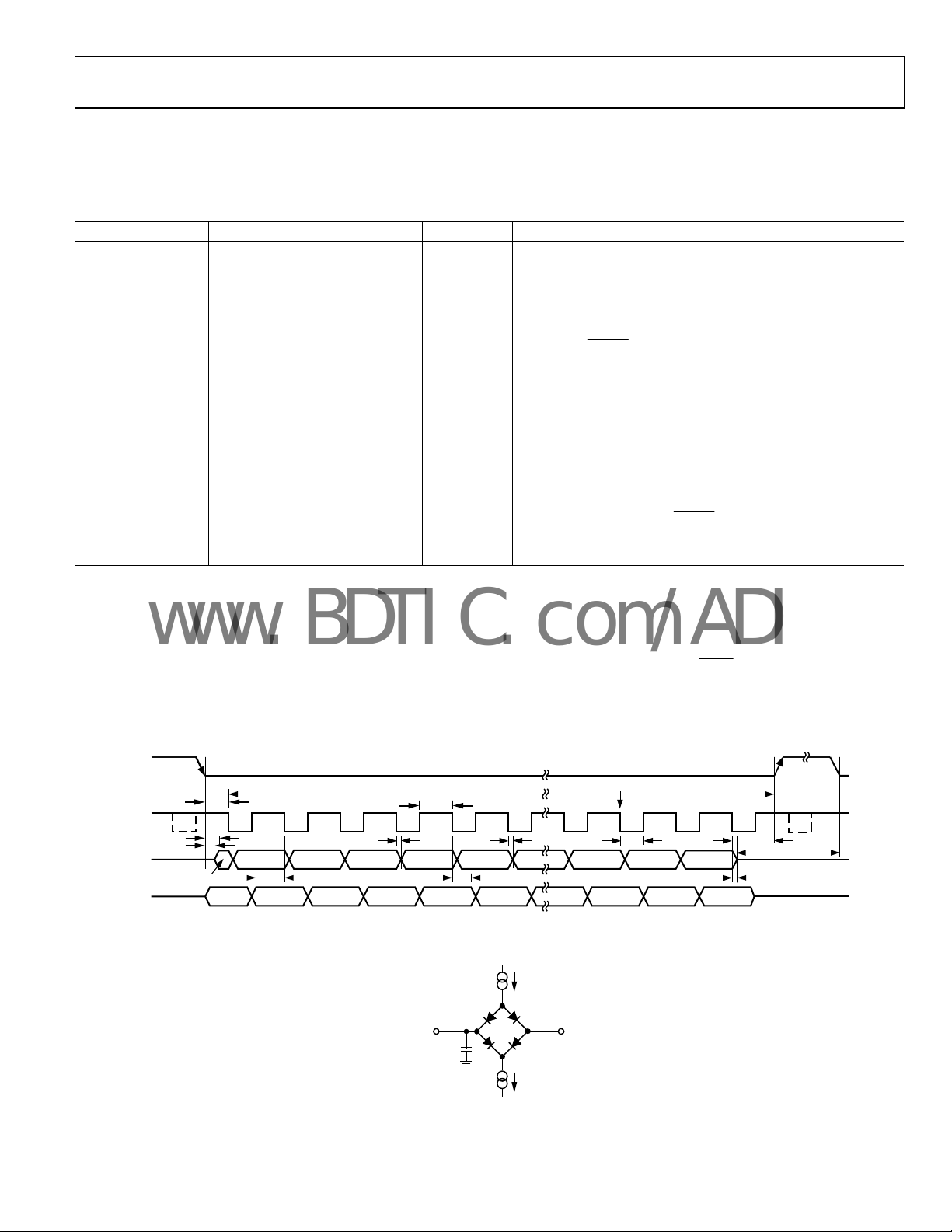
ADC Timing Characteristics
ADCVDD = 2.7 V to 5.25 V, V
Table 5.
Parameter
f
SCLK
1
Limit at T
2 10 kHz min
20 MHz min
t
16 × t
CONVER T
t
50 ns min
QUIET
t2 10 ns min
3
t
14 ns max
3
t3b4 20 ns min Data hold time
3
t
40 ns max Data access time after ASCLK falling edge
4
t5 0.4 × t
t6 0.4 × t
t7 15 ns min ASCLK to ADOUT valid hold time
5
t
8
15/50 ns min/max ASCLK falling edge to ADOUT high impedance
t9 20 ns min ADIN setup time prior to ASCLK falling edge
t10 5 ns min ADIN Hold time prior to ASCLK falling edge
t11 20 ns min
t12 1 µs max
1
Guaranteed by design and characterization. Not production tested. All input signals are specified with tr = tf = 5 ns (10% to 90% of ADCVDD) and timed from a voltage
level of 1.6 V.
2
Maximum ASCLK frequency is 50 MHz at ADCVDD = 2.7 V to 5.5 V. Guaranteed by design and characterization; not production tested.
3
Measured with the load circuit of Figure 3 and defined as the time required for the output to cross 0.4 V or 0.7 × V
4
t3b represents a worst-case figure for having ADD3 available on the ADOUT line, that is, if the ADC goes back into three-state at the end of a conversion and some
other device takes control of the bus between conversions, the user needs to wait a maximum time of t3b before having ADD3 valid on the ADOUT line. If the ADOUT
line is weakly driven to ADD3 between conversions, then the user typically needs to wait 17 ns at 3 V and 12 ns at 5 V after the
valid on ADOUT.
5
t8 is derived from the measured time taken by the data outputs to change 0.5 V when loaded with the circuit of Figure 3. The measured number is then extrapolated
back to remove the effects of charging or discharging the 25 pF capacitor. This means that the time, t8, quoted in the timing characteristics, is the true bus relinquish
time of the part and is independent of bus loading.
≤ ADCVDD, V
DRIVE
, T
MIN
MHz max
ASCLK
; ADCVDD = 5 V Unit Conditions/Comments
MAX
= 2.5 V; All specifications T
REFA
to T
MIN
to ASCLK setup time
ASYNC
MAX
Delay from ASYNC
ns min ASCLK low pulse width
ASCLK
ns min ASCLK high pulse width
ASCLK
th
ASCLK falling edge to ASYNC high
16
Power-up time from full power-down/autoshutdown/
autostandby modes
, unless otherwise noted.
until ADOUT three-state disabled
.
DRIVE
ASYNC
falling edge before seeing ADD3
ASYNC
ASCLK
DOUT
ADIN
t
THREE-
STATE
t
t
2
1 2 3 4 5 6 13 14 15 16
t
b
3
ADD3
3
ADD2 ADD1 ADD0 DB 11 DB10 DB2 DB1 DB0
t
FOUR IDENTIFICATION BITS
9
WRITE SEQ ADD3 ADD2 ADD1 ADD0 DONTC DONTC DONTC
t
4
t
6
CONVERT
t
10
t
7
B
t
5
Figure 2. ADC Timing Characteristics
200µA I
O OUTPUT
PIN
C
L
25pF
200µA I
Figure 3. Load Circuit for ADC Digital Output Timing Specifications
Rev. 0 | Page 9 of 44
OL
1.6V
OH
07691-003
t
11
t
8
t
QUIET
THREE-
STATE
07691-002
AD5590
www.BDTIC.com/ADI
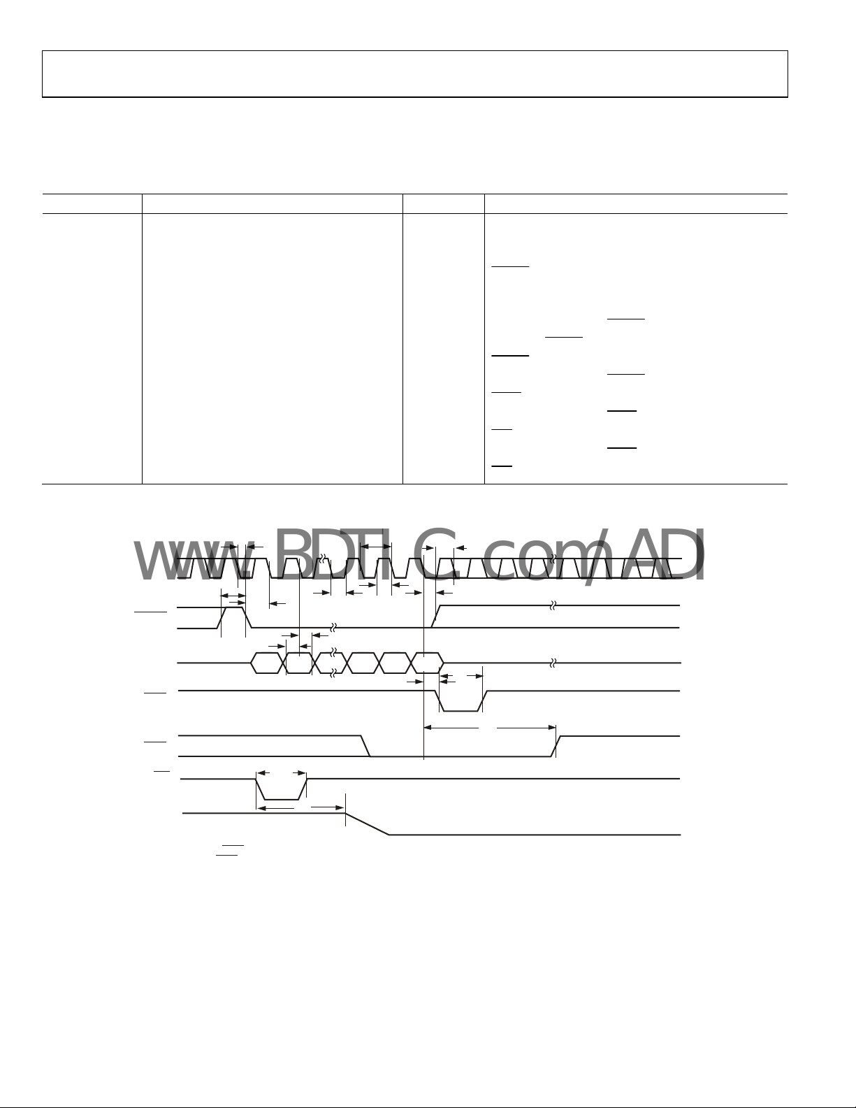
DAC Timing Characteristics
All input signals are specified with tr = tf = 1 ns/V (10% to 90% of VDD) and timed from a voltage level of (VIL + VIH)/2. See Figure 4.
DACV
Table 6.
Parameter
t
1
t2 8 ns min DSCLK high time
t3 8 ns min DSCLK low time
t4 13 ns min
t5 4 ns min Data setup time
t6 4 ns min Data hold time
t7 0 ns min
t8 15 ns min
t9 13 ns min
t10 0 ns min
t11 10 ns min
t12 15 ns min
t13 5 ns min
t14 0 ns min
t15 300 ns typ
1
Sample tested at 25°C to ensure compliance.
2
Maximum DSCLK frequency is 50 MHz at VDD = 2.7 V to 5.5 V. Guaranteed by design and characterization; not production tested.
= 4.5 V to 5.5 V. All specifications T
DD
1
2
Limit at T
20 ns min DSCLK cycle time
MIN
, T
; DACVDD = 2.7 V to 5.5 V Unit Conditions/Comments
MAX
MIN
to T
, unless otherwise noted.
MAX
to DSCLK falling edge setup time
DSYNC
DSCLK falling edge to DSYNC
Minimum DSYNC
rising edge to DSCLK fall ignore
DSYNC
DSCLK falling edge to DSYNC
pulse width low
LDAC
DSCLK falling edge to LDAC
pulse width low
CLR
DSCLK falling edge to LDAC
pulse activation time
CLR
t
DSCLK
DSYNCx
DDIN
LDAC
10
t
8
1
DB31
t
4
t
6
t
5
t
1
t
t
3
2
DB0
t
9
t
7
t
11
t
14
rising edge
high time
fall ignore
rising edge
falling edge
t
12
2
LDAC
t
CLR
VOUTx
1
ASYNCHRONOUS LDAC UPDAT E MODE.
2
SYNCHRONOUS LDAC UPDAT E MODE.
13
t
15
Figure 4. DAC Timing Characteristics
Rev. 0 | Page 10 of 44
07691-004
AD5590
www.BDTIC.com/ADI
ABSOLUTE MAXIMUM RATINGS
TA = 25°C unless otherwise noted. VDD refers to DACVDD or
ADCV
. GND refers to DACGND or ADCGND.
DD
Table 7.
Parameter Rating
VDD to GND −0.3 V to +7 V
V
to GND −0.3 V to VDD + 0.3 V
DRIVE
Op Amp Supply Voltage 6 V
Op Amp Input Voltage
Op Amp Differential Input Voltage ±6 V
Op Amp Output Short-Circuit
Duration to GND
Analog Input Voltage to GND −0.3 V to VDD + 0.3 V
Digital Input Voltage to GND −0.3 V to +7 V
Digital Output Voltage to GND −0.3 V to VDD +0.3 V
V
to GND −0.3 V to VDD +0.3 V
REFA
V
REFIN/VREFOUT
Input Current to Any ADC Pin
Except Supplies
Operating Temperature Range −40°C to +85°C
Storage Temperature Range −65°C to +150°C
Junction Temperature (TJ max) 150°C
to GND −0.3 V to VDD +0.3 V
(V1− or V2−) − 0.3 V to
(V1+ or V2+) + 0.3 V
Indefinite
±10 mA
Stresses above those listed under Absolute Maximum Ratings
may cause permanent damage to the device. This is a stress
rating only; functional operation of the device at these or any
other conditions above those indicated in the operational
section of this specification is not implied. Exposure to absolute
maximum rating conditions for extended periods may affect
device reliability.
THERMAL RESISTANCE
θJA is specified for the worst-case conditions, that is, a device
soldered in a 4-layer JEDEC thermal test board for surfacemount packages.
Table 8. Thermal Resistance
Package Type θJA Unit
80-Ball CSP_BGA 40 °C/W
Table 9. Junction Temperature
Parameter
Junction Temperature
1
P
TOTAL
2
θ
JA
is the sum of ADC, DAC, and operational amplifier supply currents.
is the package thermal resistance.
Max Unit Comments
1, 2
130 °C TJ = TA + P
TOTAL
× θ
JA
ESD CAUTION
Rev. 0 | Page 11 of 44
AD5590
www.BDTIC.com/ADI
PIN CONFIGURATION AND FUNCTION DESCRIPTIONS
121110987654321
VOUT14
VIN12
OUT7
IN7(–)
IN7(+)
IN6(+)
IN6(–)
V2–
OUT6
OUT5
IN5(–)
VOUT10
VIN10
VOUT9
VOUT11
VOUT13
VOUT15
V
REFIN2
V
REFOUT2
VIN15
V
REFA
VIN14
VIN11
/
VOUT8
VOUT12
VIN13
DACGND
VOUT1
V2+
LDAC
DACV
ADIN
DD
DDIN
DSYNC2
ASCLK
DSCLK
CLR
V
DRIVE
DSYNC1
DACGND
VIN1
DACV
VOUT3
VIN3
VOUT5
VOUT7
VIN8
VOUT2
VOUT4
VOUT6
V
REFIN1
REFOUT1
VIN5
V1–
VIN7
VIN6
VIN4
VOUT0
/
DD
VIN9
V
VIN2
OUT2
IN2(+)
IN2(–)
IN3(+)
IN3(–)
OUT3
OUT1
IN1(–)
IN1(+)
OUT0
A
B
C
D
E
F
G
H
J
K
L
IN5(+)
IN4(+)
IN4(–)
OUT4
Table 10. Pin Function Descriptions
Pin No. Mnemonic Description
M7
Frame Synchronization Signal. Active low logic input. This input provides the dual function of
ASYNC
initiating ADC conversions and also frames the serial data transfer.
J11 V
REFA
Reference Input for the ADC Block. An external reference must be applied to this input. The voltage
range for the external reference is 2.5 V ± 1% for specified performance.
M8 ADCVDD
Power Supply Input for the ADC Block. The ADC can operate from 4.5 V to 5.25 V, and the supply
should be decoupled with a 10 µF in parallel with a 0.1 µF capacitor to ADCGND.
M5 ADCGND
Ground Reference Point for the ADC Block. All ADC analog/digital input/output signals and any
external reference signal should be referred to this ADCGND voltage.
M4, L5, L3, L4, L2,
G2, K2, J2, B2, B3,
B11, L11, B12, L10,
K11, H11
VIN0 to
VIN15
Analog Input 0 through Analog Input 15. Sixteen single-ended analog input channels that are
multiplexed into the on-chip track and hold. The analog input channel to be converted is selected by
using the ADD3 through ADD0 address bits of the control register. The address bits in conjunction
with the SEQ and shadow bits allow the sequence register to be programmed. The input range for all
input channels can extend from 0 V to V
control register. Any unused input channels should be connected to GND to avoid noise pickup.
L8 ADIN
ADC Data In. Logic input. Data to be written to the control register of the ADC is provided on this input and
is clocked into the register on the falling edge of ASCLK (see the Accessing the ADC Block section).
M6 ADOUT
Data Out. Logic output. The conversion result from the ADC block is provided on this output as a serial
data stream. The bits are clocked out on the falling edge of the ASCLK input. The data stream consists
of four address bits indicating which channel the conversion result corresponds to, followed by the
12 bits of conversion data, which is provided MSB first. The output coding can be selected as straight
binary or twos complement via the coding bit in the control register.
ASYNC
ADCV
DD
Figure 5. Pin Configuration
ADOUT
ADCGND
or 0 V to 2 × V
REFA
VIN0
V1+
IN0(+)
IN0(–)
M
7691-005
, as selected via the range bit in the
REFA
Rev. 0 | Page 12 of 44

AD5590
www.BDTIC.com/ADI
Pin No. Mnemonic Description
L7 ASCLK
L6 V
DRIVE
A4, B8 DACVDD
A9, B5 DACGND
A8
A5
B7
B6
LDAC
DSYNC1
DSYNC2
Asynchronous Clear Input. The CLR input is falling edge sensitive. When CLR is low, all LDAC pulses are
CLR
A7 DDIN
A6 DSCLK
A1, B9, C2, B4, D2,
A3, E2, A2
A10, C11, B11, D11,
B10, E11, A12, F11
F2
G11
VOUT0 to
VOUT7
VOUT8 to
VOUT15
/
V
REFIN1
V
REFOUT1
/
V
REFIN2
V
REFOUT2
M3 V1+
H2 V1− Negative Supply Input for Amplifier 0 to Amplifier 3.
L9 V2+
H12 V2− Negative Supply Input for Amplifier 4 to Amplifier 7.
M1, J1, D1, F1, M10,
L12, G12, D12
M2, K1, C1, E1, M11,
M12, F12, E12
L1, H1, B1, G1, M9,
K12, J12, C12
IN0(−) to
IN7(−)
IN0(+) to
IN7(+)
OUT0 to
OUT7
Serial Clock. Logic input. ASCLK provides the serial clock for accessing data from the ADC block. This
clock input is also used as the clock source for the conversion process of the ADC.
Logic Power Supply Input. The voltage supplied at this pin determines at what voltage the serial
interface of the ADC block operates.
Power Supply Input for the DAC Block. The DAC can operate from 4.5 V to 5.25 V, and the supply
should be decoupled with a 10 µF in parallel with a 0.1 µF capacitor to DACGND. The two DACV
DD
must be connected together.
Ground Reference Point for the DAC Block. All DAC analog/digital input/output signals and any
external reference signal should be referred to this DACGND voltage. The two DACGND pins should be
connected together.
Pulsing this pin low allows any or all DAC registers to be updated if the input registers have new data.
This allows all DAC outputs to simultaneously update. Alternatively, this pin can be tied permanently
low.
Active Low Control Input. This is the frame synchronization signal for the input data of DAC channels
VOUT0 to VOUT7. When DSYNC1
input shift register. Data is transferred in on the falling edges of the next 32 clocks. If DSYNC1
nd
high before the 32
falling edge, the rising edge of DSYNC1 acts as an interrupt and the write
goes low, it powers on the DSCLK and DDIN buffers and enables the
is taken
sequence is ignored by the device.
Active Low Control Input. This is the frame synchronization signal for the input data of DAC channels
VOUT8 to VOUT15. When DSYNC2
input shift register. Data is transferred in on the falling edges of the next 32 clocks. If DSYNC2
high before the 32
nd
falling edge, the rising edge of DSYNC2 acts as an interrupt and the write
goes low, it powers on the DSCLK and DDIN buffers and enables the
is taken
sequence is ignored by the device.
ignored. When CLR
is activated, the input register and the DAC register are updated with the data
contained in the CLR code register—zero scale, midscale, or full scale. Default setting clears the output
to 0 V.
DAC Data Input. This DAC has a 32-bit shift register. Data is clocked into the register on the falling
edge of the serial clock input.
DAC Clock Input. Data is clocked into the input shift register on the falling edge of the serial clock
input. Data can be transferred at rates of up to 50 MHz.
Analog Output Voltage from DAC0 to DAC7. DSYNC1 is the frame synchronization signal for writing
data to these DACs. The DAC is updated automatically if LDAC
is low, or on the falling edge of LDAC if
it is high. The output amplifiers have rail-to-rail operation.
Analog Output Voltage from DAC8 to DAC15. DSYNC2 is the frame synchronization signal for writing
data to these DACs. The DAC is updated automatically if LDAC
is low, or on the falling edge of LDAC if
it is high. The output amplifiers have rail to rail operation.
Reference Input/Output Pin for DAC0 to DAC7. The DACs have a common pin for reference input and
reference output. When using the internal reference, this is the reference output pin. When using an
external reference, this is the reference input pin. The default for this pin is as a reference input.
Reference Input/Output Pin for DAC8 to DAC15. The DACs have a common pin for reference input and
reference output. When using the internal reference, this is the reference output pin. When using an
external reference, this is the reference input pin. The default for this pin is as a reference input.
Positive Supply Input for the amplifier 0 to amplifier 3. The supply for these amplifiers is independent
of other supplies and can be operated with a different supply if required. The pin should be decoupled
to V1− with a 10 µF in parallel with a 0.1 µF capacitor.
Positive Supply Input for Amplifier 4 to Amplifier 7. The supply for these amplifiers is independent of
other supplies and can be operated with a different supply if required. The pin should be decoupled
to V2− with a 10 µF in parallel with a 0.1 µF capacitor.
Inverting Input Terminals for Operational Amplifier 0 to Amplifier 7.
Noninverting Input Terminals for Operational Amplifier 0 to Amplifier 7.
Output Terminals for Operational Amplifier 0 to Amplifier 7.
pins
Rev. 0 | Page 13 of 44
AD5590
www.BDTIC.com/ADI
TYPICAL PERFORMANCE CHARACTERISTICS
DAC
DACVDD and ADCVDD = 5 V, VSY = 5 V, unless otherwise noted.
1.0
DACVDD = V
T
= 25°C
0.8
A
0.6
0.4
0.2
0
–0.2
INL ERROR (LSB)
–0.4
–0.6
–0.8
–1.0
0 500 1000 1500 2000 2500 3000 3500 4000
REF
= 5V
CODE
Figure 6. DAC INL, External Reference Figure 9. DAC DNL, Internal Reference
07691-006
0.20
DACVDD = 5V
V
= 2.5V
REFOUT
0.15
TA = 25°C
0.10
0.05
0
–0.05
DNL ERRO R (LSB)
–0.10
–0.15
–0.20
01000500 20001500 350030002500 4000
CODE
7691-009
0.20
DACVDD = V
T
= 25°C
A
0.15
0.10
0.05
0
–0.05
DNL ERROR (LSB)
–0.10
–0.15
–0.20
0 500 1000 1500 2000 2500 3000 3500 4000
REF
= 5V
CODE
Figure 7. DAC DNL, External Reference Figure 10. DAC Gain Error and Full-Scale Error vs. Temperature
1.0
DACVDD = 5V
V
REFOUT
T
= 25°C
A
= 2.5V
CODE
0.8
0.6
0.4
0.2
0
–0.2
INL ERRO R (LS B)
–0.4
–0.6
–0.8
–1.0
01000500 20001500 350030002500 4000
Figure 8. DAC INL, Internal Reference Figure 11. DAC Zero-Scale Error and Offset Error vs. Temperature
0
DACVDD = 5V
–0.02
–0.04
–0.06
–0.08
–0.10
–0.12
ERROR (% F SR)
–0.14
–0.16
–0.18
–0.20
7691-007
7691-008
–40 –20 40200 1008060
1.5
1.0
0.5
0
–0.5
ERROR (mV)
–1.0
–1.5
OFFSET ERROR
–2.0
–2.5
–40 –20 40200860 100
GAIN ERROR
FULL-SCAL E ERROR
TEMPERATURE (°C)
ZERO-SCALE ERROR
TEMPERATURE (°C)
07691-010
0
07691-011
Rev. 0 | Page 14 of 44

AD5590
www.BDTIC.com/ADI
0.50
DAC LOADED WIT H
FULL-SCAL E
0.40
SOURCING CURRENT
0.30
0.20
0.10
0
–0.10
ERROR VOLTAGE (V)
–0.20
–0.30
–0.40
–0.50
–10 –8 –6 –4 –2 0 2 4 8610
DACVDD= 5V
V
= 2.5V
REFOUT
CURRENT (mA)
Figure 12. DAC Headroom at Rails vs. Source and Sink
DAC LOADED WIT H
ZERO-SCALE
SINKING CURRENT
DACVDD = V
T
= 25°C
A
DACV
1
2
CH1 2.0V CH2 500mV M100 µs 125MS/s
7691-012
DD
VOUT
A CH1 1.28V
= 5V
REFA
MAX(C2)*
420.0mV
8.0ns/pt
07691-015
Figure 15. DAC Power-On Reset to 0 V
6
DACVDD= 5V
V
= 2.5V
REFOUT
5
T
= 25°C
A
4
3
(V)
OUT
V
2
1
0
–1
–30 –20 –10 0 10 20 30
CURRENT (mA)
FULL SCALE
3/4 SCALE
MIDSCALE
1/4 SCALE
ZERO SCALE
Figure 13. DAC Sink and Source Capability
DACVDD = V
T
= 25°C
A
FULL-SCALE CODE CHANGE
0x0000 TO 0xFFFF
OUTPUT LOADED WITH 2kΩ
AND 200pF TO GND
V
= 909mV/DIV
OUT
1
TIME BASE = 4µs/DIV
REFA
= 5V
Figure 14. DAC Full-Scale Settling Time
DSYNC
1
3
2
CH1 5.0V
7691-013
CH3 5.0V
DSCLK
VOUT
DACVDD = 5V
CH2 500mV M400ns A CH1 1.4V
7691-016
Figure 16. DAC Exiting Power-Down to Midscale
2.505
2.504
2.503
2.502
2.501
2.500
2.499
2.498
2.497
2.496
(V)
2.495
OUT
2.494
V
2.493
2.492
2.491
2.490
2.489
2.488
2.487
2.486
07691-014
2.485
0 512
64 128 192 256 320 384 448
DACVDD = 5V
= 2.5V
V
REFOUT
T
= 25°C
A
4ns/SAMPL E NUMBER
GLITCH IMPULSE = 3.55nV-sec
1 LSB CHANGE AROUND
MIDSCALE (0 x8000 TO 0x7FF F)
SAMPLE
07691-017
Figure 17. DAC Digital-to-Analog Glitch Impulse (Negative)
Rev. 0 | Page 15 of 44

AD5590
www.BDTIC.com/ADI
2.5000
2.4995
2.4990
2.4985
2.4980
(V)
2.4975
OUT
V
2.4970
2.4965
2.4960
2.4955
2.4950
0 512
64 128 192 256 320 384 448
SAMPLE
DACVDD = 5V
V
REFOUT
= 25°C
T
A
4ns/SAMPL E NUMBER
Figure 18. DAC Analog Crosstalk
= 2.5V
07691-018
DACVDD = 5V
= 2.5V
V
REFOUT
= 25°C
T
A
DAC LOADED WITH MIDSCALE
1
10µV/DIV
5s/DIV
Figure 20. 0.1 Hz to 10 Hz DAC Output Noise Plot, Internal Reference
07691-020
2.4900
2.4895
2.4890
2.4885
2.4880
(V)
OUT
2.4875
V
2.4870
2.4865
2.4860
2.4855
0 512
64 128 192 256 320 384 448
SAMPLE
DACVDD = 5V
V
REFOUT
= 25°C
T
A
4ns/SAMPL E NUMBER
Figure 19. DAC-to-DAC Crosstalk
= 2.5V
800
TA = 25°C
MIDSCALE LO ADED
700
600
500
400
300
OUTPUT NOISE (nV/ √Hz)
200
100
0
100 100001000 100000 1000000
07691-019
Figure 21. DAC Noise Spectral Density, Internal Reference
DACVDD= 5V
V
= 2.5V
REFOUT
FREQUENCY ( Hz)
7691-021
Rev. 0 | Page 16 of 44

AD5590
–
www.BDTIC.com/ADI
20
DACVDD = 5V
T
= 25°C
A
–30
DAC LOADED WITH FULL SCALE
V
= 2V ±0.3V p-p
REF
–40
–50
–60
(dB)
–70
–80
–90
–100
2k 4k 6k 8k 10k
Figure 22. DAC Total Harmonic Distortion Figure 24. DAC Multiplying Bandwidth
FREQUENCY ( Hz)
7691-022
5
0
–5
–10
–15
(dB)
–20
–25
–30
–35
–40
10k 100k 1M 10M
FREQUENCY (Hz)
DACVDD = 5V
T
A
= 25°C
07691-024
16
V
= DACV
REFIN
TA = 25°C
14
12
10
TIME (µs)
8
6
4
012 34567 981
DD
CAPACITANCE (nF)
DACV
5V
=
DD
Figure 23. DAC Settling Time vs. Capacitive Load
0
7691-023
Rev. 0 | Page 17 of 44

AD5590
–
–
www.BDTIC.com/ADI
ADC
DACVDD and ADCVDD = 5 V, VSY = 5 V, unless otherwise noted.
5
–15
–35
–55
(dB)
–75
–95
0 50 100 150 200 250 300 350 400 500
FREQUENCY ( kHz)
8192 POINT FFT
f
= 1MSPS
SAMPLE
f
= 50kHZ
IN
SINAD = 70.697d B
THD = –79.171dB
SFDR = –79.93d B
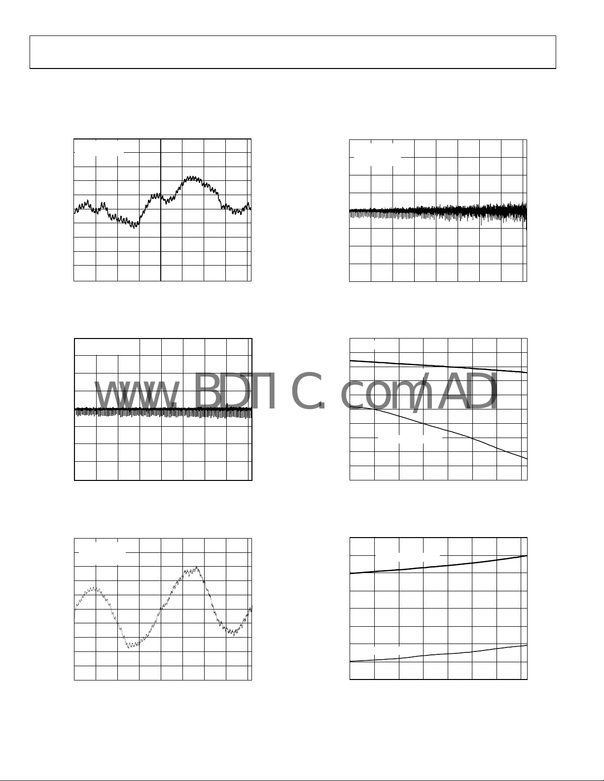
Figure 25. ADC Dynamic Performance at 1 MSPS
450
07691-025
50
f
= 1MSPS
S
T
= 25°C
A
–55
ADCV
= 5.25V
DD
RANGE = 0V TO REF
–60
–65
(dB)
–70
–75
= 5Ω
R
–80
–85
IN
10 100 1000
IN
= 100Ω
R
IN
R
= 10Ω
IN
INPUT FREQ UENCY (Hz)
RIN = 1000Ω
Figure 28. ADC THD vs. Input Frequency for Various
Analog Source Impedances
7691-028
75
ADCVDD = V
70
ADCVDD = V
65
(dB)
60
f
= MAX THROUGHPUT
S
T
= 25°C
A
RANGE = 0V TO V
55
10 100 1000
REFA
INPUT F REQUE NCY (kHz)
DRIVE
DRIVE
= 5.25V
= 4.75V
07691-026
Figure 26. ADC SINAD vs. Analog Input Frequency
for Various Supply Voltages at 1 MSPS
50
f
= MAX THROUGHPUT
S
= 25°C
T
A
–55
RANGE = 0V TO REF
–60
–65
–70
(dB)
–75
–80
–85
–90
10 100 1000
IN
ADCVDD = V
ADCV
INPUT FREQ UENCY (kHz)
= 4.75V
DRIVE
= V
DRIVE
= 5.25V
7691-027
DD
Figure 27. THD vs. Analog Input Frequency for Various Supplies at 1 MSPS
1.0
ADCVDD = V
0.8
TEMPERATURE = 25°C
0.6
0.4
0.2
0
–0.2
INL ERROR (LSB)
–0.4
–0.6
–0.8
–1.0
0 512 1024 1536 2048 2560 3072 3584 4096
DRIVE
= 5V
CODE
Figure 29. ADC Typical INL
1.0
ADCVDD = V
0.8
TEMPERATURE = 25°C
0.6
0.4
0.2
0
–0.2
DNL ERROR (LSB)
–0.4
–0.6
–0.8
–1.0
0 512 1024 1536 2048 2560 3072 3584 4096
DRIVE
= 5V
CODE
Figure 30. ADC Typical DNL
07691-029
07691-030
Rev. 0 | Page 18 of 44

AD5590
www.BDTIC.com/ADI
AMPLIFIER
DACVDD and ADCVDD = 5 V, VSY = 5 V, unless otherwise noted.
1800
VSY = 5.5V
NUMBER OF AMPLIF IERS
1600
1400
1200
1000
800
600
400
200
–0.5V < V
T
0
–2000
A
= 25°C
–1700
< +5.5V
CM
–800
–500
–1100
–1400
INPUT OFFSET VOLTAGE (µV)
–200
100
400
Figure 31. Amplifier Input Offset Voltage Distribution
700
1000
1900
1300
1600
07691-031
400
VSY = 5V
350
300
250
200
150
100
INPUT BIAS CURRENT (pA)
50
0
25 150
50 75 100 125
TEMPERATURE (°C)
Figure 34. Amplifier Input Bias Current vs. Temperature
07691-034
40
35
30
25
20
15
NUMBER OF AMPLIF IERS
10
5
0
01
123456789
TCV
(µV/°C)
OS
–40°C < TA < +125°C
V
= 2.5V
CM
0
07691-032
Figure 32. Amplifier Input Offset Voltage Drift Distribution
2000
1500
1000
–500
–1000
INPUT OFFSET VOLTAGE (µV)
–1500
500
0
VSY = 5V
T
= 25°C
A
50
VSY = ±2.5V
40
30
20
10
AMPLIFIER SUPPLY CURRENT (µA)
0
–40
–10205080110
Figure 35. Amplifier Supply Current vs. Temperature
1k
VSY = 5V
= 25ºC
T
A
100
10
1
0.1
OUTPUT SATURATION VOLTAGE (mV)
TEMPERATURE (° C)
VSY – V
SOURCE
SINK
V
OL
07691-035
OH
–2000
–0.5 5.5
0 0.5 1.0 1.5 2.0 2.5 3.0 3.5 4.0 4.5 5.0
INPUT COMMO N-MODE VOL TAGE (V)
07691-033
Figure 33. Amplifier Input Offset Voltage vs. Input Common-Mode Voltage
0.01
0.001 10
0.01 0.1 1
Figure 36. Amplifier Output Saturation Voltage vs. Load Current
Rev. 0 | Page 19 of 44
LOAD CURRENT (mA)
07691-036

AD5590
www.BDTIC.com/ADI
40
30
VSY = 5V
VSY – VOH @ 1mA
120
100
VSY = 5V
T
= 25°C
A
80
20
VOL @ 1mA
10
OUTPUT SATURATION VOLTAGE (mV)
0
–25 –10 5 20 35 50 65 80 95 110
–40 125
TEMPERATURE (°C)
07691-037
Figure 37. Amplifier Output Saturation Voltage vs. Temperature (IL = 1 mA)
350
VSY = 5V
300
250
200
150
100
50
OUTPUT SATURATION VOLTAGE (mV)
0
–40 125
VDD – VOH @ 10mA
VOL @ 10mA
–25 –10 5 20 35 50 65 80 95 110
TEMPERATURE (°C)
07691-038
Figure 38. Amplifier Output Saturation Voltage vs. Temperature (IL = 10 mA)
60
CMRR (dB)
40
20
0
100 1M
1k 10k
FREQUENCY (Hz)
100k
Figure 40. Amplifier CMRR vs. Frequency
120
VSY = ±2.5V
T
= 25°C
A
100
80
60
PSRR (dB)
40
20
0
100 1M
1k 10k 100k
FREQUENCY (Hz)
Figure 41. Amplifier PSRR vs. Frequency
07691-040
07691-041
60
50
40
30
20
10
OPEN-LOOP GAIN (dB)
0
VSY = ±2.5V
–10
R
= 100kΩ
L
C
= 20pF
L
–20
1k 1M
10k 100k
FREQUENCY ( Hz)
Figure 39. Amplifier Open-Loop Gain and Phase vs. Frequency
135
90
45
Ф
M
0
OPEN-LO OP PHASE SHIF T (Degr ees)
–45
07691-039
1k
AV = 100
100
AV = 10
10
OUTPUT IMPEDANCE (Ω)
1
0
100 1M
1k 10k 100k
Figure 42. Amplifier Closed-Loop Output Impedance vs. Frequency
Rev. 0 | Page 20 of 44
AV = 1
FREQUENCY (Hz)
VSY = 5V
07691-042

AD5590
www.BDTIC.com/ADI
50
VSY = 5V
T
= 25°C
A
45
40
35
30
25
20
15
10
SMALL SIGNAL OVERSHOOT (%)
5
0
10 1000
LOAD CAPACITANCE ( pF)
–OS
+OS
100
Figure 43. Small Signal Overshoot vs. Load Capacitance
07691-043
0
(V)V
OUT
V
–2.5
100
(mV)
IN
0
TIME (20µs/DIV)
Figure 46. Amplifier Positive Overload Recovery
VSY = ±2.5V
A
= –50
V
07691-046
VSY = 5V
A
= 1
V
R
= 10kΩ
L
C
= 200pF
L
VOLTAGE (50mV/DIV)
TIME (4µs/DIV)
Figure 44. Amplifier Small Signal Transient Response
VSY = 5V
A
= 1
V
R
= 10kΩ
L
C
= 200pF
L
VOLTAGE (1V/DIV)
2.5
(V)
OUT
V
0
0
(mV)
IN
V
–100
07691-044
TIME (20µs/ DIV)
VSY = ±2.5V
A
= –50
V
07691-047
Figure 47. Amplifier Negative Overload Recovery
V
IN
V
OUT
VOLTAGE (1V/DIV)
VSY = ±2.5V
A
= 1
V
R
= 10kΩ
L
V
= 6V p-p
IN
TIME (20µs/DIV)
Figure 45. Amplifier Large Signal Transient Response
07691-045
Figure 48. Amplifier, No Phase Reversal
Rev. 0 | Page 21 of 44
TIME (20µs/DIV)
07691-048

AD5590
www.BDTIC.com/ADI
VSY = 5V
140
120
100
VSY = 5V
80
60
VOLTAGE NOISE (1µV/DIV)
TIME (1s/ DIV)
Figure 49. Amplifier 0.1 Hz to 10 Hz Input Voltage Noise
1000
VSY = 5V
= 25°C
T
A
100
10
INPUT VOLTAGE NOISE (nV/√Hz)
1
1 10000
1/F CORNER @ 100Hz
10 100 1000
FREQUENCY (Hz)
Figure 50. Amplifier Voltage Noise Density
40
CHANNEL SEPARATION (dB)
20
07691-049
0
100 1M
1k 10k 100k
FREQUENCY (Hz)
07691-051
Figure 51. Amplifier Channel Separation
07691-050
Rev. 0 | Page 22 of 44

AD5590
www.BDTIC.com/ADI
TERMINOLOGY
DAC Integrated Nonline arity
For the DAC, relative accuracy, or integral nonlinearity (INL),
is a measure of the maximum deviation in LSBs from a straight
line passing through the endpoints of the DAC transfer function.
DAC Differential Nonlinearity
Differential nonlinearity (DNL) is the difference between the
measured change and the ideal 1 LSB change between any two
adjacent codes. A specified differential nonlinearity of ±1 LSB
maximum ensures monotonicity. The DAC is guaranteed
monotonic by design.
DAC Offs et Error
Offset error is a measure of the difference between the actual
V
and the ideal V
OUT
region of the transfer function. It can be negative or positive
and is expressed in millivolts.
DAC Zero-Code Error
Zero-code error is a measure of the output error when zero
code (0x0000) is loaded into the DAC register. Ideally, the
output should be 0 V. The zero-code error is always positive
because the output of the DAC cannot go below 0 V. It is due
to a combination of the offset errors in the DAC and output
amplifier. Zero-code error is expressed in millivolts.
DAC Gai n Erro r
Gain error is a measure of the span error of the DAC. It is the
deviation in slope of the DAC transfer characteristic from the
ideal, expressed as a percentage of the full-scale range.
DAC Zero-Code Error Drift
Zero-code error drift is a measure of the change in zero-code
error with a change in temperature. It is expressed in microvolts
per degree Celsius.
DAC Gain Error Drift
Gain error drift is a measure of the change in gain error with
changes in temperature. It is expressed in ppm of full-scale
range per degree Celsius.
DAC Fu l l -Scale Er ror
Full-scale error is a measure of the output error when full-scale
code (0xFFFF) is loaded into the DAC register. Ideally, the output should be V
percentage of the full-scale range. Figure 10 shows a plot of
typical full-scale error vs. temperature.
DAC Digital-to-Analog Glitch Impulse
Digital-to-analog glitch impulse is the impulse injected into the
analog output when the input code in the DAC register changes
state. It is normally specified as the area of the glitch in nV-sec
and is measured when the digital input code is changed by 1
LSB at the major carry transition (0x7FFF to 0x8000).
, expressed in millivolts in the linear
OUT
− 1 LSB. Full-scale error is expressed as a
DD
DAC DC Power Supply Rejection Ratio (PSRR)
PSRR indicates how the output of the DAC is affected by changes
in the supply voltage. PSRR is the ratio of the change in V
to a change in DACV
measured in decibels. V
varied ±10%.
DAC DC Crosstalk
DC crosstalk is the dc change in the output level of one DAC
in response to a change in the output of another DAC. It is
measured with a full-scale output change on one DAC (or
soft power-down and power-up) while monitoring another
DAC kept at midscale. It is expressed in microvolts.
DC crosstalk due to load current change is a measure of the
impact that a change in load current on one DAC has to
another DAC kept at midscale. It is expressed in microvolts
per milliamp.
Reference Feedthrough
Reference feedthrough is the ratio of the amplitude of the signal
at the DAC output to the reference input when the DAC output
is not being updated (that is,
decibels.
DAC Digital Feedthrough
Digital feedthrough is a measure of the impulse injected into
the analog output of a DAC from the digital input pins of the
device, but is measured when the DAC is not being written to
SYNC
(
held high). It is specified in nV-sec and measured with
a full-scale change on the digital input pins, that is, from all 0s
to all 1s or vice versa.
DAC Dig ital Cro sstalk
Digital crosstalk is the glitch impulse transferred to the output
of one DAC at midscale in response to a full-scale code change
(all 0s to all 1s or vice versa) in the input register of another
DAC. It is measured in standalone mode and is expressed in
nV-sec.
DAC Analog Crosstalk
Analog crosstalk is the glitch impulse transferred to the output
of one DAC due to a change in the output of another DAC. It is
measured by loading one of the input registers with a full-scale
code change (all 0s to all 1s or vice versa) while keeping
high, and then pulsing
of the DAC whose digital code has not changed. The area of the
glitch is expressed in nV-sec.
DAC-to-DAC Crosstalk
DAC-to-DAC crosstalk is the glitch impulse transferred to the
output of one DAC due to a digital code change and subsequent
output change of another DAC. This includes both digital and
analog crosstalk. It is measured by loading one of the DACs with a
full-scale code change (all 0s to all 1s or vice versa) with
low and monitoring the output of another DAC. The energy of
the glitch is expressed in nV-sec.
for full-scale output of the DAC. It is
DD
is held at 2 V, and DACVDD is
REFIN
LDAC
is high). It is expressed in
LDAC
low and monitoring the output
OUT
LDAC
LDAC
Rev. 0 | Page 23 of 44

AD5590
(
+−−
www.BDTIC.com/ADI
Multiplying Bandwidth
The amplifiers within the DAC have a finite bandwidth. The
multiplying bandwidth is a measure of this. A sine wave on the
reference (with full-scale code loaded to the DAC) appears on
the output. The multiplying bandwidth is the frequency at
which the output amplitude falls to 3 dB below the input.
DAC Total Harmonic Distortion (THD)
Total harmonic distortion is the difference between an ideal
sine wave and its attenuated version using the DAC. The sine
wave is used as the reference for the DAC, and the THD is a
measure of the harmonics present on the DAC output. It is
measured in decibels.
ADC Differential Nonlinearity
This is the difference between the measured and the ideal 1 LSB
change between any two adjacent codes in the ADC.
ADC Integral Nonlinearity
This is the maximum deviation from a straight line passing
through the endpoints of the ADC transfer function. The
endpoints of the transfer function are zero scale, a point 1 LSB
below the first code transition, and full scale, a point 1 LSB
above the last code transition.
ADC Offset Error
This is the deviation of the first code transition (00…000 to
00…001) from the ideal, that is, ADCGND + 1 LSB.
ADC Offset Error Match
This is the difference in offset error between any two channels.
ADC Gain Error
This is the deviation of the last code transition (111…110
to 111…111) from the ideal (that is, V
− 1 LSB) after the
REFA
offset error has been adjusted out.
ADC Gain Error Match
This is the difference in gain error between any two channels.
ADC Zero-Code Error
This applies when using the twos complement output coding
option, in particular to the 2 × V
to +V
biased about the V
REFA
REFA
midscale transition (all 0s to all 1s) from the ideal V
that is, V
− 1 LSB.
REFA
input range with−V
REFA
REFA
point. It is the deviation of the
voltage,
IN
ADC Zero-Code Error Match
This is the difference in ADC zero-code error between any two
channels.
ADC Positive Gain Error
This applies when using the twos complement output coding
option, in particular to the 2 × V
to +V
biased about the V
REFA
REFA
input range with −V
REFA
REFA
point. It is the deviation of the
last code transition (011…110 to 011…111) from the ideal (that
is, +V
− 1 LSB) after the zero-code error has been adjusted out.
REFA
ADC Positive Gain Error Match
This is the difference in ADC positive gain error between any
two channels.
ADC Negative Gain Error
This applies when using the twos complement output coding
option, in particular to the 2 × V
to +V
biased about the V
REFA
input range with −V
REFA
point. It is the deviation of
REFA
REFA
the first code transition (100…000 to 100…001) from the
ideal (that is, −V
+ 1 LSB) after the ADC zero-code error
REFA
has been adjusted out.
ADC Negative Gain Error Match
This is the difference in negative gain error between any two
channels.
ADC Channel-to-Channel Isolation
Channel-to-channel isolation is a measure of the level of
crosstalk between channels. It is measured by applying a fullscale 400 kHz sine wave signal to all 15 nonselected input
channels and determining how much that signal is attenuated
in the selected channel with a 50 kHz signal. The figure is given
worst case across all 16 channels for the ADC.
ADC PSR (Power Supply Rejection)
Variations in power supply affect the full scale transition, but
not the linearity of the converter. Power supply rejection is the
maximum change in full-scale transition point due to a change
in power supply voltage from the nominal value (see the Typ ic a l
Performance Characteristics section).
ADC Track-and-Hold Acquisition Time
The track-and-hold amplifier returns into track on the 14
th
ASCLK falling edge. Track-and-hold acquisition time is the
minimum time required for the track-and-hold amplifier to
remain in track mode for its output to reach and settle to within
±1 LSB of the applied input signal, given a step change to the
input signal.
ADC Signal-to-(Noise + Distortion) Ratio
This is the measured ratio of signal to (noise + distortion) at the
output of the analog-to-digital converter. The signal is the rms
amplitude of the fundamental. Noise is the sum of all nonfundamental signals up to half the sampling frequency (f
/2), excluding
S
dc. The ratio is dependent on the number of quantization levels
in the digitization process; the more levels, the smaller the quantization noise. The theoretical signal-to-(noise + distortion) ratio
for an ideal N-bit converter with a sine wave input is given by
)
NDistortionNoisetoSignal
[dB]76.102.6+=
Thus, for a 12-bit converter, this is 74 dB.
ADC Total Harmonic Distortion
Total harmonic distortion (THD) is the ratio of the rms sum of
harmonics to the fundamental. For the ADC, it is defined as
22222
VVVVV
++++
THD
where
V
V
, V5, and V6 are the rms amplitudes of the second through the
4
×=
log20[dB]
is the rms amplitude of the fundamental and V2, V3,
1
V
1
65432
sixth harmonics.
Rev. 0 | Page 24 of 44

AD5590
www.BDTIC.com/ADI
ADC Peak Harmonic or Spurious Noise
Peak harmonic or spurious noise is defined as the ratio of the
rms value of the next largest component in the ADC output
spectrum (up to f
fundamental. Normally, the value of this specification is determined by the largest harmonic in the spectrum, but for ADCs
where the harmonics are buried in the noise floor, it is a
noise peak.
ADC Intermodulation Distortion
With inputs consisting of sine waves at two frequencies, fa
and fb, any active device with nonlinearities creates distortion
products at sum and difference frequencies of mfa ± nfb, where
m, n = 0, 1, 2, 3, and so on. Intermodulation distortion terms
are those for which neither m nor n are equal to zero. For
/2 and excluding dc) to the rms value of the
S
example, the second-order terms include (fa + fb) and (fa − fb),
while the third-order terms include (2fa + fb), (2fa − fb), (fa +
2fb), and (fa − 2fb).
The ADC is tested using the CCIF standard where two input
frequencies near the top end of the input bandwidth are used.
In this case, the second-order terms are usually distanced in
frequency from the original sine waves whereas the third-order
terms are usually at a frequency close to the input frequencies.
As a result, the second- and third-order terms are specified
separately. The calculation of the intermodulation distortion
is as per the THD specification, where it is the ratio of the rms
sum of the individual distortion products to the rms amplitude
of the sum of the fundamentals expressed in decibels.
Rev. 0 | Page 25 of 44

AD5590
www.BDTIC.com/ADI
THEORY OF OPERATION
The AD5590 is an analog I/O module. The output port contains
sixteen 12-bit voltage output DAC channels. The DAC channels
are divided into two groups of eight DACs, each of which can be
programmed independently. Each group of DACs contains its
own internal 2.5 V reference. The references are powered down
by default allowing the use of external references, if required.
Either internal reference can be powered up and used as a reference for the ADC section. This is achieved by connecting the
appropriate V
V
pins have different input and output impedances it is
REFOUTx
REFINx/VREFOUTx
pin to V
. Because the V
REFA
REFINx
/
not possible to use one internal reference for both DAC groups
without buffering.
The input port comprises a single, 12-bit, 1 MSPS ADC with
16 multiplexed input channels. The ADC contains a sequencer
that allows it to sample any combination of the sixteen channels.
The AD5590 also contains eight rail-to-rail low noise amplifiers.
These amplifiers can be used independently or as part of signal
condition for the input or output ports.
Resistor String
The resistor string section is shown in Figure 53. It is simply
a string of resistors, each of Value R. The code loaded into
the DAC register determines at which node on the string the
voltage is tapped off to be fed into the output amplifier. The
voltage is tapped off by closing one of the switches connecting
the string to the amplifier. Because it is a string of resistors, it is
guaranteed monotonic.
R
R
R
TO OUTPUT
AMPLI FIER
DAC SECTION
Sixteen DACs make up the output port of the AD5590. Each
DAC consists of a string of resistors followed by an output
buffer amplifier. The sixteen DACs are divided into two groups
of eight with each group having its own internal 2.5 V reference
with an internal gain of 2. Figure 52 shows a block diagram of
the DAC architecture.
DACV
DD
REF (+)
DAC REGISTER
RESISTOR
STRING
REF (–)
GND
Figure 52. DAC Architecture
AMPLIFIER
(GAI N = +2)
Because the input coding to the DAC is straight binary, the ideal
output voltage when using an external reference is given by
REFIN
⎛
×=
⎟
⎜
N
2
⎠
⎝
OUT
VV
D
⎞
The ideal output voltage when using the internal reference is
given by
D
⎞
VV
2
REFOUTOUT
⎛
××=
⎟
⎜
N
2
⎠
⎝
where:
D = decimal equivalent of the binary code that is loaded to the
DAC register (0 to 4095).
N = 12.
OUTPUT
VOUTx
07691-052
R
R
07691-053
Figure 53. Resistor String
DAC Internal Reference
The DAC section has two on-chip 2.5 V references with
an internal gain of 2, giving a full-scale output of 5 V. The
on-board reference is off at power-up, allowing the use of
an external reference. The internal references are enabled
via a write to the appropriate control register (see Tab l e 11 ).
The internal references associated with each group of DACs
are available at the V
REFIN1/VREFOUT1
and V
REFIN2/VREFOUT2
pins. A
buffer is required if the reference output is used to drive external
loads. When using the internal reference, it is recommended
that a 100 nF capacitor be placed between the reference output
and DACGND for reference stability.
Individual channel power-down is not supported while using
the internal reference.
DAC Output Amplifier
The output buffer amplifier can generate rail-to-rail voltages on
its output, which gives an output range of 0 V to DACV
DD
. The
amplifier is capable of driving a load of 2 kΩ in parallel with
1000 pF to DACGND. The source and sink capabilities of the
output amplifier can be seen in Figure 13. The slew rate is
1.5 V/µs with a ¼ to ¾ scale settling time of 10 µs.
Rev. 0 | Page 26 of 44

AD5590
V
A
www.BDTIC.com/ADI
ADC SECTION
The ADC section is a fast, 16-channel, 12-bit, single-supply,
analog-to-digital converter. The ADC is capable of throughput
rates of up to 1 MSPS when provided with a 20 MHz clock.
The ADC section provides the user with an on-chip trackand-hold, analog-to-digital converter. The ADC section has
16 single-ended input channels with a channel sequencer,
allowing the user to select a sequence of channels through
which the ADC can cycle with each consecutive
ASYNC
falling
edge. The serial clock input accesses data from the ADC, controls
the transfer of data written to the ADC, and provides the clock
source for the successive approximation ADC converter. The
analog input range for the ADC is 0 V to V
depending on the status of Bit 1 in the control register.
V
REFA
or 0 V to 2 ×
REFA
The ADC provides flexible power management options to
allow the user to achieve the best power performance for a
given throughput rate. These options are selected by programming the power management bits in the ADC control register.
ADC CONVERTER OPERATION
The ADC is a 12-bit successive approximation analog-to-digital
converter based around a capacitive DAC. The ADC can convert
analog input signals in the range 0 V to V
Figure 54 and Figure 55 show simplified schematics of the ADC.
The ADC comprises control logic, SAR, and a capacitive DAC,
which are used to add and subtract fixed amounts of charge
from the sampling capacitor to bring the comparator back
into a balanced condition. Figure 54 shows the ADC during
its acquisition phase. SW2 is closed and SW1 is in Position
A. The comparator is held in a balanced condition and the
sampling capacitor acquires the signal on the selected VIN
channel.
VIN0
VIN15
ADCGND
A
SW1
Figure 54. ADC Acquisition Phase
4kΩ
B
SW2
When the ADC starts a conversion (see Figure 55), SW2 opens
and SW1 moves to Position B, causing the comparator to become
unbalanced. The control logic and the capacitive DAC are used
to add and subtract fixed amounts of charge from the sampling
capacitor to bring the comparator back into a balanced condition. When the comparator is rebalanced, the conversion is
complete. The control logic generates the ADC output code.
Figure 57 shows the ADC transfer function.
or 0 V to 2 × V
REFA
COMPARATOR
CAPACITIVE
DAC
CONTROL
LOGIC
REFA
VIN0
VIN15
ADCGND
A
SW1
Figure 55. ADC Conversion Phase
4kΩ
B
SW2
COMPARATOR
Analog Input
Figure 56 shows an equivalent circuit of the analog input structure
of the ADC. The two diodes, D1 and D2, provide ESD protection
for the analog inputs. Care must be taken to ensure that the analog
input signal never exceed the supply rails by more than 200 mV.
This causes these diodes to become forward biased and start
conducting current into the substrate. 10 mA is the maximum
current these diodes can conduct without causing irreversible
damage to the ADC. Capacitor C1 in Figure 56 is typically about
4 pF and can primarily be attributed to pin capacitance. Resistor
R1 is a lumped component made up of the on resistance of a
switch (track-and-hold switch) and also includes the on resistance of the input multiplexer.
DCV
.
INx
C1
4pF
Figure 56. Equivalent Analog Input Circuit
DD
D1
D2
CONVERSION PHASE—SWITCH OPEN
TRACK PHASE—SWI TCH CLOSED
R1
The total resistance is typically about 400 Ω. Capacitor C2 is
the ADC sampling capacitor and typically has a capacitance of
30 pF. For ac applications, removing high frequency components
from the analog input signal is recommended by use of an RC
low-pass filter on the relevant analog input pin. In applications
where harmonic distortion and signal-to-noise ratio are critical,
drive the analog input from a low impedance source. Large
source impedances significantly affect the ac performance of
the ADC. This may necessitate the use of an input buffer
07691-054
amplifier. The choice of the op amp is a function of the
particular application.
When no amplifier is used to drive the analog input, limit the
source impedance to low values. The maximum source impedance
depends on the amount of total harmonic distortion (THD) that
can be tolerated. The THD increases as the source impedance
increases, and performance degrades (see Figure 28).
C2
30pF
CAPACITIVE
DAC
CONTROL
LOGIC
07691-056
07691-055
Rev. 0 | Page 27 of 44

AD5590
www.BDTIC.com/ADI
ADC Transfer Function
The output coding of the ADC is either straight binary or twos
complement, depending on the status of the LSB (range bit) in
the ADC control register. The designed code transitions occur
midway between successive LSB values (that is, 1 LSB, 2 LSBs,
and so on). The LSB size is equal to V
/4096. The ideal transfer
REFA
characteristic for the ADC when straight binary coding is selected
is shown in Figure 57.
111.. .111
111. ..110
111...000
REF
REF
/4096
– 1LSB
7691-057
011...111
000...010
000...001
000...000
V
REF
1LSB +V
0V
IS EITHER V
Figure 57. Straight Binary Transfer Characteristic
REFA
OR 2 × V
1LSB = V
ANALOG INPUT
REFA
011...111
011...110
000...001
000...000
111.. .111
ADC CODE
100...010
100...001
100...000
+ 1LSB
REFA
Figure 58. Twos Complement Transfer Characteristic with
V
REFA
– 1LSB
V
REFA
ANALOG INPUT
± V
Input Range
REFA
1LSB = 2 × V
+V
REFA
REFA
– 1LSB–V
/4096
07691-058
Analog Input Selection
Any one of 16 analog input channels can be selected for conversion
by programming the multiplexer with the ADD3 to ADD0
address bits in the ADC control register. The channel configurations are shown in Tab l e 2 3 . The ADC can also be configured to
automatically cycle through a number of channels as selected.
The sequencer feature is accessed via the SEQ and shadow bits
in the ADC control register (see Tabl e 21 ). The ADC can be
programmed to continuously convert on a selection of channels
in ascending order. The analog input channels to be converted
on are selected through programming the relevant bits in the
shadow register (see Ta ble 2 6). The next serial transfer then acts
on the sequence programmed by executing a conversion on the
lowest channel in the selection.
The next serial transfer results in a conversion on the next
highest channel in the sequence, and so on. It is not necessary
to write to the ADC control register once a sequencer operation
Rev. 0 | Page 28 of 44
has been initiated. The write bit must be set to 0 to ensure
the ADC control register is not accidentally overwritten, or
the sequence operation interrupted. If the ADC control register
is written to at any time during the sequence, then it must be
ensured that the SEQ and shadow bits are set to 1 and 0,
respectively to avoid interrupting the automatic conversion
sequence. This pattern continues until the ADC is written to
and the SEQ and shadow bits are configured with any bit
combination except 1, 0. On completion of the sequence, the
ADC sequencer returns to the first selected channel in the shadow
register and commence the sequence again if uninterrupted.
Rather than selecting a particular sequence of channels, a number
of consecutive channels beginning with Channel 0 can also be
programmed via the control register alone, without needing
to write to the shadow register. This is possible if the SEQ and
shadow bits are set to 1, 1. The channel address bits, ADD3
through ADD0, then determine the final channel in the consecutive sequence. The next conversion is on Channel 0, then
Channel 1, and so on until the channel selected via the ADD3
through ADD0 address bits is reached. The cycle begins again
on the next serial transfer provided the write bit is set to low
or, if high, that the SEQ and shadow bits are set to 1, 0; then,
the ADC continues its preprogrammed automatic sequence
uninterrupted. Regardless of which channel selection method
is used, the 16-bit word output from the ADC during each
conversion always contains the channel address that the conversion result corresponds to, followed by the 12-bit conversion
result (see the Serial Interface section).
Digital Inputs
The digital inputs applied to the ADC are not limited by the
maximum ratings that limit the analog inputs. Instead, the
digital inputs applied can go to 7 V and are not restricted
by the ADCV
Another advantage of ASCLK, ADIN, and
restricted by the ADCV
supply sequencing issues are avoided. If
ASCLK is applied before ADCV
+ 0.3 V limit found on the analog inputs.
DD
ASYNC
not being
+ 0.3 V limit is the fact that power
DD
ASYNC
, ADIN, or
, there is no risk of latch-up
DD
as there would be on the analog inputs if a signal greater than
0.3 V was applied prior to ADCV
V
DRIVE
The ADC has the V
feature, which controls the voltage at
DRIVE
which the serial interface operates. V
DD
.
allows the ADC to
DRIVE
easily interface to both 3 V and 5 V processors. For example, if
the ADC is operated with a V
of 5 V, the V
DD
pin could be
DRIVE
powered from a 3 V supply. The ADC has better dynamic performance with a V
processors. Care should be taken to ensure that V
exceed ADCV
of 5 V while still being able to interface to 3 V
DD
does not
DRIVE
by more than 0.3 V (see the Absolute Maximum
DD
Ratings section).

AD5590
www.BDTIC.com/ADI
Reference Section
An external reference source should be used to supply the 2.5 V
reference to the ADC. Errors in the reference source results in
gain errors in the ADC transfer function and adds to the specified
full-scale errors of the ADC. A capacitor of at least 0.1 μF should
be placed on the V
ADC include the AD780, REF193, and the AD1852.
If 2.5 V is applied to the V
either be 0 V to 2.5 V or 0 V to 5 V, depending on the range bit
in the control register.
pin. Suitable reference sources for the
REFA
pin, the analog input range can
REFA
The parts are fully specified to operate from a single 5.0 V
supply, or ±2.5 V dual supplies. The ability to swing rail-to-rail
at both the input and output enables designers to buffer CMOS
ADCs, DACs, ASICs, and other wide output swing devices in
low power, single-supply systems. The amplifiers in the AD5590
are fully independent of the DAC and ADC sections. If some or
all of the amplifiers are not required, connect them as a
grounded unity-gain buffer, as shown in Figure 59.
AMPLIFIER SECTION
The operational amplifiers in the AD5590 are micropower,
rail-to-rail input and output amplifiers that feature low supply
current, low input voltage, and low current noise.
07691-059
Figure 59. Configuration for Unused Amplifiers
Rev. 0 | Page 29 of 44

AD5590
www.BDTIC.com/ADI
SERIAL INTERFACE
The AD5590 contains independent serial interfaces for the
ADC and DAC sections. The ADC uses the
ADIN, and ADOUT pins. The V
pin allows the user to
DRIVE
ASYNC
, ASCLK,
determine the output voltage of logic high signals. The DAC
uses DSCLK, DDIN,
DSYNC1
DSYNC2, LDAC
,
, and
CLR
.
The 16 analog input channels use the ADC interface. The 16
output channels use the DAC interface. The 16 output channels
are divided into two groups of eight channels, which can be
controlled independently. Each group has its own set of control
registers. When addressing the DAC control registers, the serial
data should be framed by
DSYNC1
for DAC0 to DAC7 and framed by
to access the control registers
DSYNC2
to access the control
of operation. At this stage, the
or be brought high. In either case, it must be brought high for
a minimum of 15 ns before the next write sequence so that a
falling edge of
DSYNCx
DAC Input Shift Register
The input shift register is 32 bits wide (see Figure 61). The first
four bits are don’t cares. The next four bits are the command
bits, C3 to C0 (see Tab le 11), followed by the 4-bit DAC address,
A3 to A0 (see Tabl e 12 ), and finally the 12-bit data-word. The
data-word comprises the 12-bit input code followed by eight
don’t care bits. These data bits are transferred to the DAC
nd
register on the 32
falling edge of DSCLK.
registers for DAC8 to DAC15.
The interfaces are compatible with SPI®, QSPI™, MICROWIRE™,
and most DSPs.
ACCESSING THE DAC BLOCK
Figure 4 shows a timing diagram of a typical write sequence to
the DAC block. The write sequence begins by bringing one or
both of the
DSYNC
lines low. If
data is written to the DAC block containing DAC0 to DAC7.
DSYNC2
If
is brought low, the data is written to the DAC block
containing DAC8 to DAC15. If both
brought low, the data is written into both blocks simultaneously.
shows how the serial interface is arranged. Figure 60
DSYNC1
DSYNC1
is brought low, the
DSYNC2
and
are
Table 11. DAC Command Definitions
Command
C3 C2 C1 C0 Description
0 0 0 0 Write to Input Register n
0 0 0 1 Update DAC Register n
0 0 1 0
Write to Input Register n, update all
(Software LDAC
0 0 1 1 Write to and update DAC Channel n
0 1 0 0 Power down/power up DAC
0 1 0 1 Load clear code register
0 1 1 0
Load LDAC
0 1 1 1 Reset (power-on reset)
1 0 0 0 Set up internal REF register
CLR
LDAC
1 0 0 1 Reserved
… … … … Reserved
1 1 1 1 Reserved
DSYNC1
DSCLK
DDIN
GROUP 1
CONTROL
REGISTERS
DAC 0
DAC 7
VOUT0
VOUT7
Table 12. DAC Address Commands
Address (n) Selected DAC Channel
A3 A2 A1 A0
VOUT8
VOUT15
07691-060
DSYNC2
GROUP 2
CONTROL
REGISTERS
Figure 60. DAC Serial Interface Configuration
DAC 8
DAC 15
Data from the DDIN line is clocked into the 32-bit shift register
on the falling edge of DSCLK. The serial clock frequency can be
as high as 50 MHz, making the AD5590 compatible with high
nd
speed DSPs. On the 32
falling clock edge, the last data bit is
0 0 0 0 DAC0 DAC8
0 0 0 1 DAC1 DAC9
0 0 1 0 DAC2 DAC10
0 0 1 1 DAC3 DAC11
0 1 0 0 DAC4 DAC12
0 1 0 1 DAC5 DAC13
0 1 1 0 DAC6 DAC14
0 1 1 1 DAC7 DAC15
1 1 1 1 DAC0 to DAC7 DAC8 to DAC15
clocked in and the programmed function is executed, that is,
a change in DAC register contents and/or a change in the mode
DB31 (MSB) DB0 (LSB)
X
XXX
C3 C2 C1 C0 A3 A2 A1 A0 D11 D10 D9 D8 D7 D6 D5 D4 D3 D2 D1 D0 X X X X X X X X
DATA BITS
DSYNCx
line can be kept low
can initiate the next write sequence.
)
register
DSYNC1
Low
DSYNC2
Low
ADDRESS BITSCOMMAND BITS
Figure 61. DAC Input Register Contents
Rev. 0 | Page 30 of 44
07691-061

AD5590
www.BDTIC.com/ADI
DSYNC
In a normal write sequence, the
32 falling edges of DSCLK, and the DAC is updated on the 32
falling edge and rising edge of
brought high before the 32
Interrupt
DSYNCx
DSYNCx
nd
falling edge, this acts as an interrupt
line is kept low for
. However, if
DSYNCx
nd
is
to the write sequence. The shift register is reset, and the write
sequence is seen as invalid. Neither an update of the DAC
register contents nor a change in the operating mode occurs
(see ). Figure 63
DAC Internal Reference Register
The on-board references in the DAC blocks are off at power-up
by default. This allows the use of an external reference if the
application requires it. The on-board references can be turned
on or off by a user-programmable internal REF register by
setting Bit DB0 high or low (see Tabl e 13). Command 1000 is
reserved for setting the internal REF register (see Ta b le 11 ).
DAC Power-On Reset
The DAC blocks contain a power-on reset circuit that controls
the output voltage during power-up. The DAC outputs power
up to 0 V. The output remains powered up at this level until a
valid write sequence is made to the DAC. This is useful in applications where it is important to know the state of the output of
the DAC while it is in the process of powering up. There is also
a software executable reset function that resets the DAC to the
power-on reset code. Command 0111 is reserved for this reset
function (see Tab le 1 1 ). Any events on
LDAC
or
CLR
during
power-on reset are ignored.
DAC Power-Down Modes
The DAC block contains four separate modes of operation.
Command 0100 is reserved for the power-down function (see
Tabl e 11 ). These modes are software-programmable by setting
Bit DB9 and Bit DB8 in the control register.
Tabl e 15 shows how the state of the bits corresponds to the mode
of operation of the device. Any or all DACs (DAC0 to DAC7 in
Block 1 or DAC8 to DAC15 in Block 2) can be powered down to
the selected mode by setting the corresponding eight bits to 1. See
Tabl e 16 for the contents of the input shift register during powerdown/power-up operation. When using the internal reference,
only all channel power-down to the selected modes is supported.
When both bits are set to 0, each block works normally with its
normal power consumption of 1.3 mA at 5 V. However, for the
three power-down modes, the supply current of each block falls
to 0.4 µA at 5 V. Not only does the supply current fall, but the
output stage is also internally switched from the output of the
amplifier to a resistor network of known values. This has the
advantage that the output impedance of the DAC is known
while it is in power-down mode. There are three different
options. The output is connected internally to GND through
either a 1 kΩ or a 100 kΩ resistor, or it is left open-circuited
(three-state). The output stage is illustrated in Figure 62.
RESISTOR
STRING DAC
Figure 62. Output Stage During Power-Down
AMPLI FIER
POWER-DOW N
CIRCUITRY
RESISTOR
NETWORK
V
OUT
07691-063
DSCLK
DSYNCx
DDIN
DB31 DB0
INVALID WRITE SEQUENCE:
SYNC HIGH BEFORE 32ND FALL ING EDGE
Figure 63.
SYNC
Interrupt Facility
DB31 DB0
VALID WRITE SEQUENCE, OUTPUT UPDATES
ON THE 32ND FALLING EDGE
Table 13. DAC Internal Reference Register
Internal REF Register (DB0) Action
0 Reference off (default)
1 Reference on
Table 14. DAC 32-Bit Input Shift Register Contents for Reference Setup Command
MSB
DB31 to DB28 DB27 DB26 DB25 DB24 DB23 DB22 DB21 DB20 DB19 to DB1 DB0
X 1 0 0 0 X X X X X 1/0
Don’t care Command bits (C3 to C0) Address bits (A3 to A0)—don’t care Don’t care Internal REF register
Rev. 0 | Page 31 of 44
LSB
07691-062

AD5590
www.BDTIC.com/ADI
The bias generator of the selected DAC(s), output amplifier,
resistor string, and other associated linear circuitry are shut
down when the power-down mode is activated. The internal
reference is powered down only when all channels are powered
down. However, the contents of the DAC register are unaffected
when in power-down. The time to exit power-down is typically
4 μs for DACV
Any combination of DACs can be powered up by setting PD1
and PD0 to 0 (normal operation). The output powers up to the
value in the input register (
DAC register before powering down (
= 5 V.
DD
LDAC
low) or to the value in the
LDAC
high).
DAC Clear Code Register
The DAC blocks have a hardware
ous clear input for all 16 DACs. The
sensitive. Bringing the
input register and the DAC registers to the data contained in
Table 15. DAC Power-Down Modes of Operation
DB9 DB8 Operating Mode
0 0 Normal operation
Power-down modes:
0 1 1 kΩ to GND
1 0 100 kΩ to GND
1 1 Three-state
CLR
CLR
pin that is an asynchron-
CLR
input is falling edge
line low clears the contents of the
the user-configurable
accordingly. This function can be used in system calibration to
load zero scale, midscale, or full scale to all channels together.
These clear code values are user-programmable by setting Bit DB1
and Bit DB0 in the
default setting clears the outputs to 0 V. Command 0101 is
reserved for loading the clear code register (see Table 11).
The DAC exits clear code mode on the 32
the next write to the DAC. If
sequence, the write is aborted.
CLR
The
when the output starts to change—is typically 280 ns. However,
if outside the DAC linear region, it typically takes 520 ns after
executing
See Table 18 for contents of the input shift register during the
loading clear code register operation.
pulse activation time—the falling edge of
CLR
CLR
register and sets the analog outputs
CLR
control register (see Table 17). The
nd
falling edge of
CLR
is activated during a write
for the output to start changing.
CLR
to
Table 16. DAC 32-Bit Input Shift Register Contents for Power-Down/Power-Up Function
MSB LSB
DB31 to
DB28 DB27 DB26 DB25 DB24 DB23 DB22 DB21 DB20
X 0 1 0 0 X X X X X PD1 PD0 DAC H DAC G DAC F DAC E DAC D DAC C DAC B DAC
Don’t care Command bits (C3 to C0) Address bits (A3 to A0)—
don’t care
Table 17. DAC Clear Code Register
Clear Code Register
DB1 DB0
CR1 CR0 Clears to Code
0 0 0x0000
0 1 0x0800
1 0 0x0FFF
1 1 No operation
Table 18. DAC 32-Bit Input Shift Register Contents for Clear Code Function
MSB LSB
DB31 to DB28 DB27 DB26 DB25 DB24 DB23 DB22 DB21 DB20 DB19 to DB2 DB1 DB0
X 0 1 0 1 X X X X X CR1 CR0
Don’t care Command bits (C3 to C0) Address bits (A3 to A0)—don’t care Don’t care Clear code register
DB19
to DB10 DB9 DB8 DB7 DB6 DB5 DB4 DB3 DB2 DB1 DB0
A
Don’t
care
Power-down
mode
Power-down/power-up channel selection—set bit to 1
to select
Rev. 0 | Page 32 of 44

AD5590
www.BDTIC.com/ADI
LDAC
Function
The outputs of all DACs can be updated simultaneously using
LDAC
the hardware
Synchronous
are updated on the falling edge of the 32
can be permanently low or pulsed as in Figure 4.
Asynchronous
time that the input registers are written to. When
low, the DAC registers are updated with the contents of the
input register.
Alternatively, the outputs of all DACs can be updated simultaneously using the software
Register n and updating all DAC registers. Command 0011 is
reserved for this software
LDAC
An
over the hardware
register gives the user extra flexibility and control
pin.
LDAC
: After new data is read, the DAC registers
LDAC
: The outputs are not updated at the same
LDAC
LDAC
function.
LDAC
pin. This register allows the user to
nd
DSCLK pulse.
function by writing to Input
LDAC
LDAC
goes
select which combination of channels to simultaneously update
when the hardware
register to 0 for a DAC channel means that this channel’s update
is controlled by the
updates synchronously; that is, the DAC register is updated
after new data is read, regardless of the state of the
It effectively registers the
Table 19 for the
flexibility is useful in applications where the user wants to
simultaneously update select channels while the rest of the
channels are synchronously updating.
Writing to the DAC using Command 0110 loads the 8-bit
LDAC
register (DB7 to DB0). The default for each channel is
0, that is, the
means the DAC channel is updated regardless of the state of
LDAC
the
register during the
pin. See Table 20 for the contents of the input shift
LDAC
pin is executed. Setting the
LDAC
pin. If this bit is set to 1, this channel
LDAC
pin as being tied low. (See
LDAC
register mode of operation.) This
LDAC
pin works normally. Setting the bits to 1
LDAC
register mode of operation.
LDAC
LDAC
bit
pin.
Table 19.
Bits (DB7 to DB0)
LDAC
0 1/0
1 X—don’t care
Table 20. DAC 32-Bit Input Shift Register Contents for
MSB
DB31
to DB28 DB27 DB26 DB25 DB24 DB23 DB22 DB21 DB20
X 0 1 1 0 X X X X X DAC H DAC G DAC F DAC E DAC D DAC C DAC B DAC A
Don’t
care
Register
LDAC
Pin
LDAC
Command bits (C3 to C0)
Address bits (A3 to A0)—
Operation
LDAC
Determined by LDAC
DAC channels update, overriding the LDAC
LDAC
don’t care
pin.
Register Function
DB19
to DB8 DB7 DB6 DB5 DB4 DB3 DB2 DB1 DB0
Don’t
care
pin. DAC channels see LDAC as 0.
Setting LDAC bit to 1 overrides LDAC pin
LSB
Rev. 0 | Page 33 of 44

AD5590
A
www.BDTIC.com/ADI
ACCESSING THE ADC BLOCK
The ADC register can be accessed via the serial interface using
the ASCLK , ADIN, ADOUT, and
ASYNC
can be used to dictate the logic levels of the output pins, allowing the ADC to be interfaced to a 3 V DSP while the ADC is
operating at 5 V.
ADC Modes of Operation
The ADC has a number of different modes of operation. These
modes are designed to provide flexible power management options.
These options can be chosen to optimize the power dissipation/
throughput rate ratio for differing application requirements.
The mode of operation of the ADC is controlled by the power
management bits, PM1 and PM0, in the ADC control register,
as detailed in Tab le 2 1. When power supplies are first applied to
the ADC, ensure that the ADC is placed in the required mode
of operation (see the Powering Up the ADC section).
Normal Mode (PM1 = PM0 = 1)
This mode is intended for the fastest throughput rate performance because the user does not have to worry about any
power-up times with the ADC remaining fully powered at all
times. Figure 64 shows the general diagram of the operation of
the ADC in this mode.
ASYNC
112
ASCLK
ADOUT
ADIN
NOTES
1. CONTROL REGISTER DATA IS LOADED ON FIRST 12 SCLK CYCLES.
2. SHADOW REG ISTER DATA IS LOADED ON FIRST 16 SCLK CYCLE S.
CHANNE L IDENTI FIER BI TS + CONV ERSION RE SULT
DATA IN TO CONTROL/ SHADOW REGI STER
Figure 64. ADC Normal Mode Operation
PART IS IN FULL
SHUTDOWN
ASYNC
116114 1614
ASCLK
pins. The V
16
PART BEGINS TO POWER UP ON ASYNC
RISING EDGE AS PM1 = 1, PM0 = 1
DRIVE
pin
07691-064
The conversion is initiated on the falling edge of
the track-and-hold enters hold mode as described in the
Interface
section. The data presented to the ADC on the ADIN
line during the first 12 clock cycles of the data transfer is loaded
to the ADC control register (provided the write bit is 1). If the
previous write had SEQ = 0 and shadow = 1, the data presented on
the ADIN line on the next 16 ASCLK cycles is loaded into the
shadow register. The ADC remains fully powered up in normal
mode at the end of the conversion as long as PM1 and PM0 are
set to 1 in the write transfer during that conversion. To ensure
continued operation in normal mode, PM1 and PM0 are both
loaded with 1 on every data transfer. Sixteen serial clock cycles
are required to complete the conversion and access the conversion result. The track-and-hold returns to track on the 14
ASYNC
ASCLK falling edge.
can then idle high until the next
conversion or can idle low until sometime prior to the next
conversion, (effectively idling
ASYNC
low).
When a data transfer is complete (ADOUT has returned to
TRI
three-state, weak/
initiated by bringing
t
, has elapsed.
QUIET
bit = 0), another conversion can be
ASYNC
low again after the quiet time,
Full Shutdown (PM1 = 1, PM0 = 0)
In this mode, all internal circuitry on the ADC is powered
down. The ADC retains information in the ADC control
register during full shutdown. The ADC remains in full
shutdown until the power management bits in the control
register, PM1 and PM0, are changed.
If a write to the ADC control register occurs while the ADC is
in full shutdown, with the power management bits changed to
PM0 = PM1 = 1, normal mode, the ADC begins to power up
on the
ASYNC
rising edge. The track-and-hold that was in hold
while the ADC was in full shutdown return to track on the 14
ASCLK falling edge.
To ensure that the ADC is fully powered up, t
ASYNC
should elapse before the next
falling edge.
shows the general diagram for this sequence.
PART IS FULLY POWERED UP
ONCE T
t
12
POWER UP
HAS ELAPSED
ASYNC
POWER-UP
Figure 65
(t12)
and
Serial
th
th
DOUT
ADIN
DATA IN TO CONTROL REGIST ER
CONTROL REGI STER IS LO ADED ON THE
FIRST 12 CLOCKS, PM 1 = 1, PM0 = 1
Figure 65. Full Shutdown Mode Operation
CHANNEL I DENTIFIER BITS + CONVERSIO N RESULT
DATA IN TO CONTROL/SHADOW REGI STER
TO KEEP PART IN NORMAL MODE, LOAD
PM1 = 1, PM0 = 1 IN CONTROL REGISTER
Rev. 0 | Page 34 of 44
07691-065

AD5590
A
www.BDTIC.com/ADI
AutoShutdown (PM1 = 0, PM0 = 1)
In this mode, the ADC automatically enters shutdown at the
end of each conversion when the ADC control register is updated.
When the ADC is in shutdown, the track-and-hold is in hold
mode. Figure 66 shows the general diagram of the operation of
the ADC in this mode. In shutdown mode, all internal circuitry
on the ADC is powered down. The ADC retains information in
the ADC control register during shutdown. The ADC remains
ASYNC
in shutdown until the next
ASYNC
this
falling edge, the track-and-hold that was in hold
falling edge it receives. On
while the ADC was in shutdown returns to track. Wake-up time
from autoshutdown is 1 µs, and the user should ensure that 1 µs
has elapsed before attempting a valid conversion. When running
the ADC with a 20 MHz clock, one dummy cycle of 16 × ASCLKs
should be sufficient to ensure that the ADC is fully powered up.
During this dummy cycle, the contents of the ADC control
register should remain unchanged; therefore, the write bit
should be 0 on the ADIN line. This dummy cycle effectively
halves the throughput rate of the ADC, with every other
conversion result being valid. In this mode, the power
consumption of the ADC is greatly reduced with the ADC
entering shutdown at the end of each conversion. When the
ADC control register is programmed to move into
autoshutdown, it does so at the end of the conversion. The user
can move the ADC in and out of the low power state by
controlling the
ASYNC
signal.
PART ENTERS
SHUTDOWN ON ASYNC
RISING EDGE AS
PM1 = 0, PM0 = 1
PART BEGINS
TO POWER
UP ON ASYNC
FALLING EDGE
Autostandby (PM1 = PM0 = 0)
In this mode, the ADC automatically enters standby mode at
the end of each conversion when the ADC control register is
updated. Figure 67 shows the general diagram of the operation
of the ADC in this mode. When the ADC is in standby, portions
of the ADC are powered down, but the on-chip bias generator
remains powered up. The ADC retains information in the ADC
control register during standby. The ADC remains in standby
until it receives the next
ASYNC
falling edge. On this
ASYNC
falling edge, the track and hold that was in hold while the ADC
was in standby returns to track. Wake-up time from standby is 1
µs; the user should ensure that 1 µs has elapsed before attempting a
valid conversion on the ADC in this mode. When running the
ADC with a 20 MHz clock, one dummy cycle of 16 × ASCLKs
should be sufficient to ensure the ADC is fully powered up.
During this dummy cycle, the contents of the ADC control register
should remain unchanged; therefore, the write bit should be set
to 0 on the ADIN line. This dummy cycle effectively halves the
throughput rate of the ADC with every other conversion result
being valid. In this mode, the power consumption of the ADC
is greatly reduced with the ADC entering standby at the end of
each conversion. When the ADC control register is programmed
to move into autostandby, it does so at the end of the conversion. The user can move the ADC in and out of the low power
state by controlling the
PART IS FULLY
POWERED U P
ASYNC
signal.
P
RT ENTERS
SHUTDOWN O N CS
RISING EDGE AS
PM1 = 0, PM0 = 1
ASYNC
ASCLK
ADOUT
ADIN
11611611
CHANNEL IDENTIFI ER BITS + CONVERSI ON RESULT
DATA IN TO CONTROL/ SHADOW REGISTER
CONTRO L REGIS TER IS LO ADED ON THE
FIRST 12 CLOCKS, PM1 = 0, PM0 = 1
CONTROL REGI STER CONTENTS SHOULD
NOT CHANGE , WRI TE BIT = 0
DUMMY CO NVERSIO N
INVALID DATA
6
CHANNEL IDENTIFI ER BITS + CONVERSI ON RESULT
DATA IN TO CONTROL/ SHADOW REG ISTER
TO KEEP PART IN THIS MODE, LOAD PM1 = 0, PM0 = 1
IN CONTROL REGISTER OR SET WRITE BIT = 0
7691-066
Figure 66. Autoshutdown Mode Operation
PART ENTERS
STANDBY O N ASYNC
RISING EDGE AS
PM1 = 0, PM0 = 0
07691-067
ASYNC
ASCLK
ADOUT
ADIN
PART ENT ERS
STANDBY O N ASYNC
RISING EDGE AS
PM1 = 0, PM0 = 0
1 12 16 1 12 16 1 12 16
CHANNEL IDENTIFIER BITS + CONVERSION RESULT
DATA IN TO CONTROL/ SHADOW RE GISTER
CONTRO L REGIST ER IS LO ADED ON THE
FIRST 12 CLOCKS, PM1 = 0, PM0 = 0
PART BEGINS
TO POWER
UP ON ASYNC
FALLING EDGE
DUMMY CONVERSIO N
INVALID DATA
CONTRO L REGIST ER CONTENTS SHOULD
REMAIN UNCHANG ED, WRITE BIT = 0
PART IS FULLY
POWERED UP
DATA IN TO CONTROL/ SHADOW REGISTER
TO KEEP PART IN THIS MODE, LOAD PM1 = 0,
PM0 = 0 IN CONTROL REG ISTER
Figure 67. Autostandby Mode Operation
Rev. 0 | Page 35 of 44

AD5590
A
V
www.BDTIC.com/ADI
Powering Up the ADC
When supplies are first applied to the ADC, the ADC can
power up in any of the operating modes of the ADC. To ensure
that the ADC is placed into the required operating mode, the
user should perform a dummy cycle operation, as outlined in
Figure 68.
The three dummy conversion operations outlined in Figure 68
must be performed to place the ADC into either of the
automatic modes. The first two conversions of this dummy
cycle operation are performed with the ADIN line tied high,
and for the third conversion of the dummy cycle operation, the
user writes the desired control register configuration to the
ADC to place the ADC into the required automode. On the
third
ASYNC
rising edge after the supplies are applied, the
control register contains the correct information and valid data
results from the next conversion.
Therefore, to ensure the ADC is placed into the correct
operating mode when supplies are first applied to the ADC,
the user must first issue two serial write operations with the
ADIN line tied high. On the third conversion cycle, the user
can then write to the ADC control register to place the ADC
into any of the operating modes. To guarantee that the ADC
control register contains the correct data, do not write to the
shadow register until the fourth conversion cycle after the
supplies are applied to the ADC.
If the user wants to place the ADC into either normal mode or
full shutdown mode, the second dummy cycle with ADIN tied
high can be omitted from the three dummy conversion operation outlined in Figure 68.
Interfacing to the ADC
Figure 2 shows the detailed timing diagram for serial interfacing to the ADC. The serial clock provides the conversion
clock and also controls the transfer of information to and from
the ADC during each conversion.
ASYNC
The
process. The falling edge of
signal initiates the data transfer and conversion
ASYNC
puts the track and hold
into hold mode, takes the bus out of three-state, and the analog
input is sampled at this point. The conversion is also initiated
at this point and requires 16 ASCLK cycles to complete. The
th
track and hold returns to track on the 14
as shown in at Point B, except when the write is to the
Figure 2
ASCLK falling edge
shadow register, in which case the track and hold does not
return to track until the rising edge of
in . On the 16
Figure 72
th
ASCLK falling edge, the ADOUT line
ASYNC
goes back into three-state (assuming the weak/
, that is, Point C
TRI
bit is set
to 0). Sixteen serial clock cycles are required to perform the
conversion process and to access data from the ADC. The
12 bits of data are preceded by the four channel address bits
(ADD3 to ADD0), identifying which channel the conversion
result corresponds to.
ASYNC
going low provides Address
Bit ADD3 to be read in by the microprocessor or DSP. The
remaining address bits and data bits are then clocked out by
subsequent ASCLK falling edges beginning with the second
Address Bit ADD2; thus, the first ASCLK falling edge on the
serial clock has Address Bit ADD3 provided and also clocks out
Address Bit ADD2. The final bit in the data transfer is valid on
th
falling edge, having being clocked out on the previous
the 16
th
) falling edge.
(15
CORRECT
REGISTER VALID DATA FROM
NEXT CONVERSION USER CAN
WRITE TO SHADOW REGISTER
ALUE IN CONTROL
IN NEXT CONVERSION
ASYNC
1 12 16 1 12 16 1 12 16
ASCLK
DOUT
ADIN
KEEP DIN LINE TIED HIG H FOR FIRS T TWO DUMMY CONVERS IONS
INVALID DATA INVALID DATA INVALID DATA
Figure 68. Placing the ADC into the Required Operating Mode after Supplies are Applied
DUMMY CONVERSIONDUMMY CONVERSION
Rev. 0 | Page 36 of 44
DATA I N TO CONTROL
CONTROL REGI STER IS L OADED ON THE
FIRST 12 CL OCK EDGES
7691-068

AD5590
www.BDTIC.com/ADI
ADC Control Register
The control register on the ADC is a 12-bit, write-only register.
Data is loaded from the ADIN pin of the ADC on the falling
edge of ASCLK. The data is transferred on the ADIN line at the
same time as the conversion result is read from the ADC. The
data transferred on the ADIN line corresponds to the ADC
configuration for the next conversion. This requires 16 serial
clocks for every data transfer. Only the information provided
on the first 12 falling clock edges (after
ASYNC
falling edge) is
loaded to the ADC control register. MSB denotes the first bit
in the data stream. The bit functions are outlined in .
Tabl e 21
Writing of information to the ADC control register takes place
on the first 12 falling edges of ASCLK in a data transfer, assuming
the MSB, that is, the write bit, has been set to 1. If the ADC
control register is programmed to use the shadow register,
writing of information to the shadow register takes place on
all 16 ASCLK falling edges in the next serial transfer (see
Figure 72
of
). The shadow register is updated on the rising edge
ASYNC
and the track-and-hold begins to track the first
channel selected in the sequence.
If the weak/
than returning to true three-state upon the 16
TRI
bit in the ADC control register is set to 1, rather
th
ASCLK falling
edge, the ADOUT line is instead pulled weakly to the logic level
corresponding to ADD3 of the next serial transfer. This is done
to ensure that the MSB of the next serial transfer is set up in
time for the first ASCLK falling edge after the
edge. If the weak/
TRI
bit is set to 0 and the ADOUT line has
been in true three-state between conversions, then depending
on the particular DSP or microcontroller interfacing to the
ADC, the ADD3 address bit may not be set up in time for the
DSP/microcontroller to clock it in successfully. In this case,
ADD3 is only driven from the falling edge of
then be clocked in by the DSP on the following falling edge of
TRI
ASCLK. However, if the weak/
bit had been set to 1, then
although ADOUT is driven with the ADD3 address bit from
the last conversion, it is nevertheless so weakly driven that
another device may still take control of the bus. It does not lead
to a bus contention (for example, a 10 kΩ pull-up or pull-down
resistor would be sufficient to overdrive the logic level of ADD3
between conversions), and all 16 channels may be identified.
However, if this does happen and another device takes control
of the bus, it is not guaranteed that ADOUT becomes fully
driven to ADD3 again in time for the read operation when
control of the bus is taken back.
This is especially useful if using an automatic sequence mode
to identify to which channel each result corresponds. Obviously,
if only the first eight channels are in use, the ADD3 address bit
does not need to be decoded, and whether it is successfully clocked
in as a 1 or 0 does not matter as long as it is still counted by the
DSP/microcontroller as the MSB of the 16-bit serial transfer.
ASYNC
ASYNC
falling
and must
Table 21. ADC Control Register
MSB
DB11 DB10 DB9 DB8 DB7 DB6 DB5 DB4 DB3 DB2 DB1 DB0
Write SEQ ADD3 ADD2 ADD1 ADD0 PM1 PM0 Shadow
Range Coding
Weak/TRI
LSB
Table 22. ADC Control Register Bit Functions
Bit Name Description
11 Write
10 SEQ
9:6 ADD3:ADD0
5, 4 PM1, PM0 These two power management bits decode the mode of operation of the ADC, as shown in Table 24.
3 Shadow
2
Weak/TRI
1 Range
0 Coding
The value written to this bit of the control register determines whether the following 11 bits are loaded to the control
register or not. If this bit is a 1, the following 11 bits are written to the control register; if it is a 0, the remaining 11 bits
are not loaded to the control register, therefore it remains unchanged.
The SEQ bit in the control register is used in conjunction with the shadow bit to control the use of the sequencer
function and to access the shadow register (see Table 25).
These four address bits are loaded at the end of the current conversion sequence and select which analog input
channel is to be converted on in the next serial transfer, or can select the final channel in a consecutive sequence, as
described in Table 25. The selected input channel is decoded as shown in Table 23 . The address bits corresponding to
the conversion result are also output on ADOUT prior to the 12 bits of data (see the Serial Interface section). The next
channel to be converted on is selected by the mux on the 14
The shadow bit in the control register is used in conjunction with the SEQ bit to control the use of the sequencer
function and access the shadow register (see Table 25).
This bit selects the state of the ADOUT line at the end of the current serial transfer. If it is set to 1, the ADOUT line is
weakly driven to the ADD3 channel address bit of the ensuing conversion. If this bit is set to 0, ADOUT returns to threestate at the end of the serial transfer. See the Serial Interface section for more details.
This bit selects the analog input range to be used on the ADC. If it is set to 0, then the analog input range extends from
0 V to 2 × V
2 × V
REFA
This bit selects the type of output coding the ADC uses for the conversion result. If this bit is set to 0, the output coding
for the ADC is twos complement. If this bit is set to 1, the output coding from the ADC is straight binary (for the next
conversion).
. If it is set to 1, then the analog input range extends from 0 V to V
REFA
, ADCVDD = 4.75 V to 5.25 V.
th
ASCLK falling edge.
(for the next conversion). For 0 V to
REFA
Rev. 0 | Page 37 of 44

AD5590
www.BDTIC.com/ADI
Table 23. ADC Channel Selection
ADD3 ADD2 ADD1 ADD0 Analog Input Channel
0 0 0 0 VIN0
0 0 0 1 VIN1
0 0 1 0 VIN2
0 0 1 1 VIN3
0 1 0 0 VIN4
0 1 0 1 VIN5
0 1 1 0 VIN6
0 1 1 1 VIN7
1 0 0 0 VIN8
1 0 0 1 VIN9
1 0 1 0 VIN10
1 0 1 1 VIN11
1 1 0 0 VIN12
1 1 0 1 VIN13
1 1 1 0 VIN14
1 1 1 1 VIN15
Table 24. ADC Power Mode Selection
PM1 PM0 Mode
1 1
1 0
0 1
0 0
ADC Sequencer Operation
The configuration of the SEQ and shadow bits in the control register allows the user to select a particular mode of operation of the
sequencer function. Tabl e 25 outlines the four modes of operation of the sequencer.
Normal operation. In this mode, the ADC remains in full power mode regardless of the status of any of the logic inputs. This
mode allows the fastest possible throughput rate from the ADC.
Full shutdown. In this mode, the ADC is in full shut down mode, with all circuitry on the ADC powered down. The ADC
retains the information in the control register while in full shutdown. The ADC remains in full shutdown until these bits are
changed in the control register.
Autoshutdown. In this mode, the ADC automatically enters shutdown mode at the end of each conversion when the control
register is updated. Wake-up time from shutdown is 1 µs and the user should ensure that 1 µs has elapsed before attempting
to perform a valid conversion on the ADC in this mode.
Autostandby. In this standby mode, portions of the ADC are powered down, but the on-chip bias generator remains
powered up. This mode is similar to autoshutdown and allows the ADC to power up within one dummy cycle, that is, 1 µs
with a 20 MHz ASCLK.
Table 25. ADC Sequence Selection
SEQ Shadow Sequence Type
0 0
0 1
1 0
1 1
This configuration means the sequence function is not used. The analog input channel selected for each individual
conversion is determined by the contents of the channel address bits, ADD0 to ADD3, in each prior write operation. This
mode of operation reflects the normal operation of a multichannel ADC, without sequencer function being used, where
each write to the ADC selects the next channel for conversion (see Figure 69).
This configuration selects the shadow register for programming. After the write to the control register, the following
write operation loads the contents of the shadow register. This programs the sequence of channels to be converted on
continuously with each successive valid ASYNC
channels selected need not be consecutive.
If the SEQ and shadow bits are set in this way, the sequence function is not interrupted upon completion of the write
operation. This allows other bits in the control register to be altered while in a sequence without terminating the cycle.
This configuration is used in conjunction with the channel address bits, ADD3 to ADD0, to program continuous
conversions on a consecutive sequence of channels from Channel 0 through to a selected final channel, as determined
by the channel address bits in the control register (see Figure 71).
falling edge (see the shadow register, , and ). The
Rev. 0 | Page 38 of 44
Table 26 Figure 70

AD5590
www.BDTIC.com/ADI
ADC Shadow Register
The shadow register on the ADC is a 16-bit, write-only register.
Data is loaded from the ADIN pin of the ADC on the falling
edge of ASCLK. The data is transferred on the ADIN line at the
same time as a conversion result is read from the ADC. This
requires 16 serial falling edges for the data transfer. The information is clocked into the shadow register, provided that the
SEQ and shadow bits were set to 0 and 1, respectively, in the
previous write to the control register. MSB denotes the first bit
in the data stream. Each bit represents an analog input from
Channel 0 through to Channel 15. A sequence of channels can
be selected through which the ADC cycles with each consecutive
ASYNC
falling edge after the write to the shadow register. To
select a sequence of channels, the associated channel bit must
be set for each analog input. The ADC continuously cycles
through the selected channels in ascending order, beginning
with the lowest channel, until a write operation occurs (that is,
the write bit is set to 1) with the SEQ and shadow bits
configured in any way except 1, 0 (see ). The bit
functions are outlined in .
Tabl e 26
Tabl e 25
Figure 69 reflects the normal operation of a multichannel ADC,
where each serial transfer selects the next channel for conversion.
In this mode of operation, the sequencer function is not used.
Figure 70 shows how to program the ADC to continuously
convert on a particular sequence of channels. To exit this mode
of operation and revert back to the normal mode of operation
of a multichannel ADC (as outlined in Figure 69), ensure the
write bit = 1 and the SEQ = shadow = 0 on the next serial
transfer.
Figure 71 shows how a sequence of consecutive channels can
be converted without having to program the shadow register
or write to the ADC on each serial transfer. Again, to exit this
mode of operation and revert back to the normal mode of
operation of a multichannel ADC (as outlined in Figure 69),
ensure the write bit = 1 and the SEQ = shadow = 0 on
the next serial transfer.
POWER ON
DUMMY CONVE RSIONS
ADIN = ALL 1s
ADIN: WRIT E TO CONT ROL REGIST ER,
ASYNC
ASYNC
WRITE BIT = 1,
SELECT C ODING, RANGE, AND POWER MODE
SELECT C HANNEL ADD3 TO CHAN NEL ADD0
FOR CONVE RSION,
SEQ = SHADOW = 0
ADOUT: CONVERSIO N RESULT FROM
PREVIOUS LY SELECTED CHANNE L ADD3 TO
CHANNEL ADD0
ADIN: WRIT E TO CONT ROL REGIST ER,
WRITE BIT = 1,
SELECT C ODING, RANGE, AND POWER MODE
SELECT C HANNEL ADD3 TO CHAN NEL ADD0
FOR CONV ERSION, SEQ = SHADO W = 0
Figure 69. Sequence Function Not Used
WRITE BIT = 1,
SEQ = SHADO W = 0
ADIN: WRITE TO CONTROL REGIS TER,
ASYNC
ASYNC
ASYNC
WRITE
BIT = 0
WRITE BIT = 1,
SELECT CODI NG, RANGE, AND POWER MODE
SELECT CHANNE L ADD3 TO CHANNEL ADD0
FOR CONVERS ION, SEQ = 0 SHADOW = 1
ADOUT: CONVERSION RESULT FRO M
PREVIOUSLY SELECTED CHANNE L ADD3 TO
CHANNEL ADD0
ADIN: WRITE TO SHADOW REGI STER,
SELECTING WHICH CHANNELS TO CONVERT
ON; CHANNELS SEL ECTED NEED NOT BE
CONSECUTIVE
WRITE BIT = 0
CONTINUOUS LY
CONVERT S ON T HE
SELECTED SEQUENCE
OF CHANNELS
Figure 70. Continuous Conversions
ADIN: WRI TE TO CONT ROL REGIST ER,
ASYNC
ASYNC
ASYNC
WRITE BIT = 1,
SELECT CODING, RANGE, AND POWE R MODE
SELECT CHANNEL ADD3 TO CHANNEL ADD0
FOR CONV ERSION, SEQ = 1 SHADOW = 1
ADOUT: CONVERSION RESULT FROM
CHANNEL 0
CONTINUO USLY CONVERTS ON A
CONSECUTI VE SEQ UENCE OF CHANNELS
FROM CHANNE L 0 UP TO AND INCLUDING
THE PREVI OUSLY SELECTED CHANNEL
ADD3 TO CHANNE L ADD0 IN THE CO NTROL
REGIST ER
CONTINUO USLY CONVERTS O N THE
SELECTED SEQUENC E OF CHANNEL S BUT
ALLOW S RANGE, CODING, AND SO ON, TO
CHANGE IN T HE CONTRO L REGISTER
WITHO UT INTERRUPTING THE SEQ UENCE
PROVIDED, SEQ = 1, SHADOW = 0
Figure 71. Continuous Conversion Without Programming
07691-069
POWER ON
DUMMY CONVERSIONS
ADIN = ALL 1s
CONTINUOUS LY
CONVERTS ON THE
SELECTED SEQUENCE
OF CHANNELS BUT
ALLOWS RANGE,
CODING, AND SO ON,
WRITE BIT = 0
POWER ON
DUMMY CONVERSIONS
ADIN = ALL 1s
TO CHANGE IN THE
CONTROL REGI STER
WITHOUT
INTERRUPTI NG THE
SEQUENCE PROV IDED,
SEQ = 1 SHADOW = 0
WRITE BIT = 1,
SEQ = 1,
SHADOW = 0
the Shadow Register
WRITE BIT = 1,
SEQ = 1, SHADOW = 0
WRITE BIT = 1,
SEQ = 1,
SHADOW = 0
WRITE
BIT = 0
WRITE BIT = 1,
SEQ = 1,
SHADOW = 0
07691-070
07691-071
Rev. 0 | Page 39 of 44

AD5590
A
www.BDTIC.com/ADI
Table 26. ADC Shadow Register Bits
MSB LSB
DB15 DB14 DB13 DB12 DB11 DB10 DB9 DB8 DB7 DB6 DB5 DB4 DB3 DB2 DB1 DB0
VIN0 VIN1 VIN2 VIN3 VIN4 VIN5 VIN6 VIN7 VIN8 VIN9 VIN10 VIN11 VIN12 VIN13 VIN14 VIN15
ASYNC
t
t
6
CONVERT
t
10
t
7
t
5
13 VIN14 VIN15
IN
t
11
t
8
ASCLK
DOUT
ADIN
THREE-
STATE
t
2
12345613141516
t
t
3
ADD3
ADD2 ADD1 ADD0 DB 11 DB10 DB2 DB1 DB0
t
FOUR IDENTIFICATION BITS
9
VIN0VIN1VIN2VIN3VIN4VIN5V
4
Figure 72. Writing to Shadow Register Timing Diagram
C
THREE-
STATE
07691-072
Rev. 0 | Page 40 of 44

AD5590
www.BDTIC.com/ADI
ADC Power vs. Throughput Rate
By operating the ADC in autoshutdown or autostandby mode,
the average power consumption of the ADC decreases at lower
throughput rates. Figure 73 shows how, as the throughput rate is
reduced, the ADC remains in its shutdown state longer and the
average power consumption over time drops accordingly.
For example, if the ADC is operated in a continuous sampling
mode with a throughput rate of 100 kSPS and an ASCLK of
20 MHz, with PM1 = 0 and PM0 = 1 (that is, the device is in
autoshutdown mode), the power consumption is calculated
as follows: the maximum power dissipation during normal
operation is 12.5 mW. If the power-up time from autoshutdown
is one dummy cycle, that is, 1 µs, and the remaining conversion
time is another cycle, that is, 1 µs, the ADC dissipates 12.5 mW
for 2 µs during each conversion cycle. For the remainder of the
conversion cycle, 8 µs, the ADC remains in shutdown mode. The
ADC dissipates 2.5 µW for the remaining 8 µs of the conversion
cycle. If the throughput rate is 100 kSPS, the cycle time is 10 µs
and the average power dissipated during each cycle is
2
10
When operating the ADC in autostandby mode, PM1 = PM0 = 0
at 5 V, 100 kSPS, the ADC power dissipation is calculated as
follows: the maximum power dissipation is 12.5 mW at 5 V during
normal operation. The power-up time from autostandby is one
dummy cycle, 1 µs, and the remaining conversion time is another
dummy cycle, 1 µs. The ADC dissipates 12.5 mW for 2 µs during
each conversion cycle. For the remainder of the conversion cycle,
8 µs, the ADC remains in standby mode dissipating 460 µW for
8
mW5.12
10
=×+×
mW502.2W5.2
8 µs. If the throughput rate is 100 kSPS, the cycle time is 10 µs
and the average power dissipated during each conversion cycle is
2
10
Figure 73 shows the power vs. throughput rate when using the
autoshutdown mode and autostandby mode with 5 V supplies.
At the lower throughput rates, power consumption for the
autoshutdown mode is lower than that for the autostandby
mode, with the ADC dissipating less power when in shutdown
compared to standby. However, as the throughput rate is
increased, the ADC spends less time in power-down states;
thus, the difference in power dissipated is negligible between
modes.
10
ADCVDD = 5V
AUTOSTANDBY
1
POWER (mV)
0.1
0.01
0 50 100 150 200 250 300 350
Figure 73. Power vs. Throughput Rate in Autoshutdown
8
mW5.12
10
=×+×
AUTOSHUTDOW N
THROUGHPUT ( kSPS)
and Autostandby Mode
mW868.2W
07691-073
Rev. 0 | Page 41 of 44

AD5590
A
www.BDTIC.com/ADI
OUTLINE DIMENSIONS
1 CORNER
INDEX AREA
8910
BOTTOM
VIEW
0.80 BSC
DETAIL A
3
4567
2
1
A
B
C
D
E
F
G
H
J
K
L
M
1.11
1.01
0.91
2.50 SQ
1.50
1.36
1.21
10.00
BSC SQ
BALL A1
PAD CORNER
TOP VIEW
DETAIL A
BSC SQ
0.60 REF
0.65 REF
0.36 REF
1112
8.80
0.35 NOM
0.30 MIN
*
COMPLIANT TO JEDEC STANDARDS MO-205-AC
WITH THE EXCEPTIO N TO BALL DIAMETER.
*
0.50
0.45
0.40
BALL DIAMET ER
SEATING
PLANE
0.12 MAX
COPLANARITY
011007-A
Figure 74. 80-Ball Chip Scale Package Ball Grid Array [CSP_BGA]
(BC-80-2)
Dimensions shown in millimeters
ORDERING GUIDE
Model Temperature Range Package Description Package Option
AD5590BBC −40°C to +85°C 80-Ball CSP_BGA BC-80-2
AD5590BBCZ
EVAL-AD5590EBZ
1
Z = RoHS Compliant Part.
1
1
−40°C to +85°C 80-Ball CSP_BGA BC-80-2
Evaluation Board
Rev. 0 | Page 42 of 44

AD5590
www.BDTIC.com/ADI
NOTES
Rev. 0 | Page 43 of 44

AD5590
www.BDTIC.com/ADI
NOTES
©2008 Analog Devices, Inc. All rights reserved. Trademarks and
registered trademarks are the property of their respective owners.
D07691-0-10/08(0)
Rev. 0 | Page 44 of 44
 Loading...