

32-Channel, 14-Bit DAC with Full-Scale Output
Voltage Programmable from 50 V to 200 V
Preliminary Technical Data
FEATURES
High integration: 32-channel, 14-bit DAC with integrated,
high voltage output amplifier
Guaranteed monotonic
Housed in 15 × 15 mm CSP-BGA package
Full-scale output voltage programmable from 50 V to 200 V
via reference input
700 µA drive capability
Integrated silicon diode for temperature monitoring
DSP-/microcontroller-compatible serial interface
Channel update rate: 1.2 MHz
Asynchronous
Temperature range: –10°C to +85°C
APPLICATIONS
Optical micro-electromechanical systems (MEMS)
Optical cross-point switches
Micropositioning applications using Piezo Flextures
Level setting in automotive test and measurement
RESET
facility
DV
CC
AV
CC
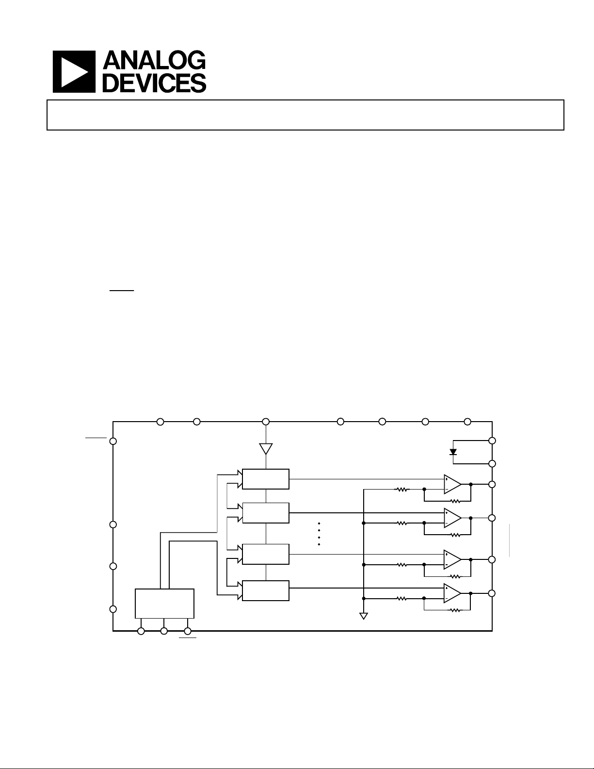
FUNCTIONAL BLOCK DIAGRAM
REF_IN
AD5535
GENERAL DESCRIPTION
The AD5535 is a 32-channel, 14-bit DAC with an on-chip high
voltage output amplifier. This device is targeted for optical
micro-electromechanical systems. The output voltage range is
programmable via the REFIN pin. Output range is 0 V to 50 V
with REFIN = 1 V and is 0 V to 200 V with REFIN = 4 V. Each
amplifier can source 700 µA, which is ideal for the deflection
and control of optical MEMS mirrors.
The selected DAC register is written to via the 3-wire interface.
The serial interface operates at clock rates of up to 30 MHz and
is compatible with DSP and microcontroller interface standards.
The device is operated with AV
to 5.25 V, V
= −4.75 V to −5.25 V, V+ = +4.75 V to +5.25 V, VPP
–
= 210 V. REF_IN is buffered internally on the AD5535 and
should be driven from a stable reference source.
V
PP
PGND
= 4.75 to 5.25 V, DVCC = 2.7 V
CC
V
–
V
+
RESET
DAC_GND
AGND
DGND
Rev. PrE
Information furnished by Analog Devices is believed to be accurate and reliable.
However, no responsibility is assumed by Analog Devices for its use, nor for any
infringements of patents or other rights of third parties that may result from its use.
Specifications subject to change without notice. No license is granted by implication
or otherwise under any patent or patent rights of Analog Devices. Trademarks and
registered trademarks are the property of their respective owners.
AD5535
INTERFACE
CONTROL
LOGIC
SCLK
D
IN
DAC
14-BIT BUS
DAC
DAC
DAC
SYNC
Figure 1.
ANODE
CATHODE
R1
RF
R1
RF
R1
RF
R1
RF
One Technology Way, P.O. Box 9106, Norwood, MA 02062-9106, U.S.A.
Tel: 781.329.4700
Fax: 781.326.8703 © 2004 Analog Devices, Inc. All rights reserved.
www.analog.com
V
0
OUT
V
1
OUT
V
30
OUT
31
V
OUT
05068-001

AD5535 Preliminary Technical Data
TABLE OF CONTENTS
Specifications..................................................................................... 3
Timing Characteristics ................................................................ 5
Absolute Maximum Ratings............................................................ 6
ESD Caution.................................................................................. 6
Pin Configuration and Function Descriptions............................. 7
Te r m in o l o g y ...................................................................................... 9
Typical Performance Characteristics........................................... 10
Functional Description ..................................................................11
Digital-to-Analog Section......................................................... 11
Reset Function ............................................................................11
Serial Interface............................................................................ 11
REVISION HISTORY
10/04—Revision PrE: Preliminary Version
Microprocessor Interfacing....................................................... 11
Applications Information.............................................................. 13
MEMS Mirror Control Application......................................... 13
AD5535 Board Layout to Ensure Compliance with IPC-221
Specification
Power Supply Sequencing and Decoupling Recommendations
....................................................................................................... 14
Guidelines for Printed Circuit Board Layout......................... 14
Outline Dimensions....................................................................... 15
Ordering Guide .......................................................................... 15
................................................................................ 13
Rev. PrE | Page 2 of 16

Preliminary Technical Data AD5535
SPECIFICATIONS
VPP = 210 V, V− = −5 V, V+ = +5 V; AVCC = 5.25 V; DVCC = 2.7 V to 5.25 V; AGND = DGND = DAC_GND = 0 V; REF_IN = 4.096 V;
all outputs unloaded. All specifications T
MIN
to T
Table 1.
Parameter
1
DC PERFORMANCE
Resolution
Integral Nonlinearity (INL)
Differential Nonlinearity (DNL)
Zero Code Voltage
Offset Error –45
Offset Drift
Voltage Gain 47.5 50 52.5 V/V
Gain Temperature Coefficient
Channel-to-Channel Gain Match
Full-Scale Voltage Drift
OUTPUT CHARACTERISTICS
Output Voltage Range
3
Output Impedance
Resistive Load
Capacitive Load
4, 5
4
Short-Circuit Current
DC Crosstalk
DC Power Supply Rejection (PSRR), V
4
PP
AC CHARACTERISTICS
Settling Time
1/4 to 3/4 Scale Step
1 LSB Step
Slew Rate
–3 dB Bandwidth 5
Output Noise Spectral Density
0.1 Hz to 10 Hz Output Noise Voltage
Digital-to-Analog Glitch Impulse
Digital Crosstalk
Analog Crosstalk
Digital Feedthrough
VOLTAGE REFERENCE, REF_IN
Input Voltage Range
6
4
1
Input Current
TEMPERATURE MEASUREMENT DIODE
4
Peak Inverse Voltage, PIV
Forward Diode Drop, VF
Forward Diode Current, IF
VF Temperature Coefficient, T
C
, unless otherwise noted.
MAX
A Grade
Min Typ Max
0
1
2
Unit Conditions/Comments
14
±0.1
Bits
% of FSR
±0.5 ±1 LSB Guaranteed monotonic
2 V
0.09
TBD
5
8
50
+45 mV
VPP – 10 V
200 pF
0.7
3 LSB
70
30
100
10
10
10
3
TBD
TBD
TBD
TBD
13
TBD
LSB/°C
ppm/°C
%
ppm/°C
Ω
MΩ
mA
dB
µs No load
µs 200 pF load
µs No load
µs 200 pF load
V/µs No load
V/µs 200 pF load
kHz
nV/√Hz
µV p-p
nV–s typ 1 LSB change around major carry
nV–s typ
µV–s typ
nV–s typ
Measured at 1 kHz
AVCC must exceed REFIN by 1.25 V min
4.096 V
1 µA
5 V Cathode to anode
0.8 V IF = 2 mA, anode to cathode
2 mA Anode to cathode
–1.44
mV/°C IF = 250 µA
Rev. PrE | Page 3 of 16

AD5535 Preliminary Technical Data
2
Unit Conditions/Comments
±5 ±10 µA
0.8 V DVCC = 3 V to 5 V
200
V DVCC = 3 V to 5 V
mV
10 pF
Parameter
DIGITAL INPUTS
1
4
Input Current
Input Low Voltage
Input High Voltage 2.0
Input Hysteresis (SCLK and
SYNC
only)
Input Capacitance
A Grade
Min Typ Max
POWER-SUPPLY VOLTAGES
VPP (50 × REF_IN) +10 210 225 V
V
–
–5.25 –4.75 V
V+ 4.75 5.25 V
AVCC 4.75 5.25 V
DVCC 2.7 5.25 V
POWER-SUPPLY CURRENTS
7
IPP 75 110 µA/channel
I
−
2.5 3.5 mA
I+ 2.5 3.5 mA
AICC 16 20 mA
DICC 0.1 0.5 mA
POWER DISSIPATION7 609 mW
1
See Terminology.
2
A Grade temperature range: −10°C to +85°C; typically +25°C.
3
Linear output voltage range: +7 V to VPP − 10 V.
4
Guaranteed by design and characterization, not production tested.
5
Ensure that TJ max is not exceeded. See the section. Absolute Maximum Ratings
6
Reference input determines output voltage range. Using a 4.096 V reference (REF 198) gives an output voltage range of 0 V to 200 V. Output range is programmable
via the reference input. The full-scale output range is programmable from 50 V to 200 V. The linear output voltage range is restricted from 7 V to V
7
Outputs unloaded.
− 10 V.
PP
Rev. PrE | Page 4 of 16
Preliminary Technical Data AD5535
TIMING CHARACTERISTICS
VPP = 210 V, V− = –5 V, V+ = +5 V; AVCC = 5.25 V; DVCC = 2.7 V to 5.25 V; AGND = DGND = DAC_GND = 0 V; REF_IN = 4.096 V.
All specifications T
MIN
to T
Table 2.
Parameter1, 2,
f
UPDATE
f
CLKIN
t
13 ns min SCLK High Pulse Width
1
t
2
t
3
t
50 ns min
4
t
5
t
10 ns min DIN Setup Time
6
t
5 ns min DIN Hold Time
7
t
8
t
20 ns min
9
3
1
See timing diagrams in Figure 2.
2
Guaranteed by design and characterization, not production tested.
3
All input signals are specified with tr = tf = 5 ns (10% to 90% of DVCC) and timed from a voltage level of (VIL + VIH)/2.
SCLK
, unless otherwise noted.
MAX
A Grade Unit Conditions/Comments
1.2 MHz max Channel Update Rate
30 MHz max SCLK Frequency
13 ns min SCLK Low Pulse Width
15 ns min
10 ns min
200 ns min
t
1
1
t
t
5
2
3
34
t
2
SYNC
Falling Edge to SCLK Falling Edge Setup Time
SYNC
Low Time
SYNC
High Time
19th SCLK Falling Edge to
RESET
Pulse Width
5
SYNC
16 17 18 19
Falling Edge for Next Write
1
SYNC
D
RESET
IN
t
9
MSB
t
4
t
6
t
7
LSB
t
8
05068-002
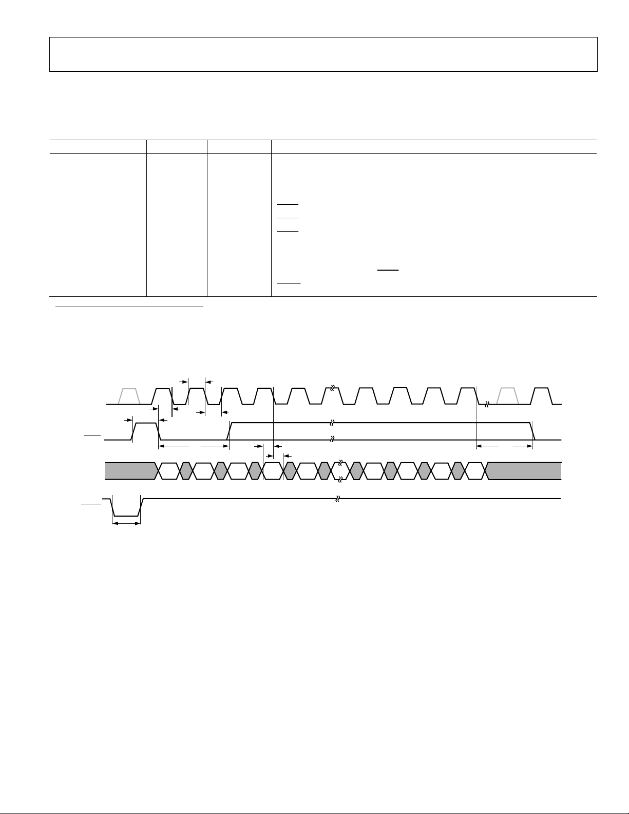
Figure 2. Serial Interface Timing Diagram
Rev. PrE | Page 5 of 16

AD5535 Preliminary Technical Data
ABSOLUTE MAXIMUM RATINGS
TA = 25°C, unless otherwise noted.
Table 3.
Parameter Rating
VPP to AGND
V− to AGND
V+ to AGND −0.3 V to +7 V
AVCC to AGND, DAC_GND −0.3 V to +7 V
DVCC to DGND −0.3 V to +7 V
Digital Inputs to DGND −0.3 V to DVCC + 0.3 V
REF_IN to AGND, DAC_GND −0.3 V to AVCC + 0.3 V
V
0–31 to AGND V– to V
OUT
Anode/Cathode to AGND, DAC_GND −0.3 V to +7 V
AGND to DGND −0.3 V to +0.3 V
Operating Temperature Range
Industrial −10°C to +85°C
Storage Temperature Range −65°C to +150°C
Junction Temperature (TJ max) 150°C
124-Lead CSP-BGA Package,
Thermal Impedance
θ
JA
Reflow Soldering
Peak Temperature 220°C
Time at Peak Temperature 10 s to 40 s
0.3 V to 225 V
+0.3 V to −6 V
PP
40°C/W
Stresses above those listed under Absolute Maximum Ratings
may cause permanent damage to the device. This is a stress
rating only; functional operation of the device at these or any
other conditions above those listed in the operational sections
of this specification is not implied. Exposure to absolute
maximum rating conditions for extended periods may affect
device reliability.
Transient currents up to 100 mA do not cause SCR latch-up.
This device is a voltage-integrated circuit with an ESD rating of
<2 kV and it is ESD sensitive. Proper precautions should be
taken for handling and assembly.
ESD CAUTION
ESD (electrostatic discharge) sensitive device. Electrostatic charges as high as 4000 V readily accumulate on
the human body and test equipment and can discharge without detection. Although this product features
proprietary ESD protection circuitry, permanent damage may occur on devices subjected to high energy
electrostatic discharges. Therefore, proper ESD precautions are recommended to avoid performance
degradation or loss of functionality.
Rev. PrE | Page 6 of 16

Preliminary Technical Data AD5535
PIN CONFIGURATION AND FUNCTION DESCRIPTIONS
3
A
B
C
D
E
F
G
H
J
K
L
M
N
P
Table 4. 124-Lead CSP-BGA Ball Configuration
CSP-BGA
Number
Ball Name
A1 N/C
A2 V
A4 V
A6 V
A8 V
A10 V
A12 V
OUT
OUT
OUT
OUT
OUT
OUT
A14 N/C
B1 V
B3 V
B5 V
B7 V
B9 V
B11 V
B13 V
C2 V
C12 V
OUT
OUT
OUT
OUT
OUT
OUT
OUT
OUT
OUT
1
7
11
16
20
25
0
4
9
13
17
21
26
3
22
CSP-BGA
Number
C14 V
D1 V
D13 V
E2 V
E4 V
E6 V
E8 V
E10 V
E12 V
E14 V
F3 V
F5 V
F7 V
F9 V
F13 V
G14 V
H1 VPP
1
2
1
6
3
5
4
5
2
4
Figure 3. Pin Configuration
Ball Name
29
OUT
2
OUT
23
OUT
5
OUT
8
OUT
12
OUT
15
OUT
19
OUT
24
OUT
31
OUT
6
OUT
10
OUT
14
OUT
18
OUT
30
OUT
28
OUT
7
11 12 13
9
10
8
9
10
876
11 12 13
14
A
B
C
D
E
F
G
H
J
K
L
M
N
P
14
CSP-BGA
Number
H2 VPP
H13 V
J3–J12 AGND
K1 V+
K2 V+
K3–K14 AGND
L1 V
L2 V
L3–L13 AGND
L14 DAC_GND
M1 AGND
M2 AGND
M3–12 AGND
M13 AVCC
M14 AVCC
N1 PGND
N2 PGND
05068-003
Ball Name
27
OUT
–
–
CSP-BGA
Number
Ball Name
N3 CATHODE
N4 ANODE
N5–N14 AGND
P1 N/C
P2 REF_IN
P3 DAC_GND
P4
RESET
P5 DVCC
P6 DGND
P7 TEST
P8 D
IN
P9 SCLK
P10
SYNC
P11–P13 AGND
P14 N/C
Rev. PrE | Page 7 of 16

AD5535 Preliminary Technical Data
Table 5. Pin Function Descriptions
Pin Function
AGND Analog GND Pins.
AV
CC
V
PP
V
V
+
V
–
PGND Output Amplifier Ground Reference Pins.
DGND Digital GND Pins.
DV
Digital Supply Pins. Voltage range from 2.7 V to 5.25 V.
CC
DAC_GND Reference GND Supply for All the DACs.
REF_IN
V
(0–31) Analog Output Voltages from the 32 Channels.
OUT
ANODE Anode of Internal Diode for Diode Temperature Measurement.
CATHODE Cathode of Internal Diode for Diode Temperature Measurement.
SYNC
1
SCLK
1
D
Serial Data Input. Data must be valid on the falling edge of SCLK.
IN
TEST
1
RESET
1
Internal pull-up device on this logic input. Therefore, it can be left floating and defaults to a logic high condition.
Analog Supply Pins. Voltage range from 4.75 V to 5.25 V.
Output Amplifier High Voltage Supply. Voltage range from (REF_IN × 50) + 10 V to 225 V.
Amplifier Supply Pins. Voltage range from 4.75 V to 5.25 V.
+
V– Amplifier Supply Pins. Voltage range from −4.75 V to −5.25 V.
Reference Voltage for Channels 0–31. Reference input range is 1 V to 4 V and can be used to program the full-scale
output voltage from 50 V to 200 V.
Active Low Input. This is the frame synchronization signal for the serial interface. While
on the falling edge of SCLK.
SYNC
is low, data is transferred in
Serial Clock Input. Data is clocked into the shift register on the falling edge of SCLK. This operates at clock speeds of up to
30 MHz.
Allows the same data to be simultaneously loaded to all channels of the AD5535. This pin is used for calibration purposes
when loading zero scale and full scale to all channels. To invoke this feature, take the TEST pin high. In normal operation,
TEST should be tied low.
Active Low Input. This pin can also be used to reset the complete device to its power-on reset conditions. Zero code is
loaded to the DACs.
Rev. PrE | Page 8 of 16

Preliminary Technical Data AD5535
TERMINOLOGY
Integral Nonlinearity (INL)
A measure of the maximum deviation from a straight line
passing through the endpoints of the DAC transfer function. It
is expressed as a percentage of full-scale range.
Differential Nonlinearity (DNL)
The difference between the measured change and the ideal
1 LSB change between any two adjacent codes. A specified DNL
of ±1 LSB maximum ensures monotonicity.
Zero-Code Voltage
A measure of the output voltage present at the device output
with all 0s loaded to the DAC. It includes the offset of the DAC
and the output amplifier. It is expressed in V.
Offset Error
Calculated by taking two points in the linear region of the
transfer function, drawing a line through these points, and
extrapolating back to the Y axis. It is expressed in mV.
Volt ag e Ga i n
Calculated from the change in output voltage for a change in
code multiplied by 16,384 and divided by the REF_IN voltage.
This is calculated between two points in the linear section of the
transfer function.
Gain Error
A measure of the output error with all 1s loaded to the DAC,
and is the difference between the ideal and actual analog output
range. Ideally, the output should be 50 × REF_IN. It is expressed
as a percentage of full-scale range.
DC Power-Supply Rejection Ratio (PSRR)
A measure of the change in analog output for a change in V
supply voltage. It is expressed in dB. V
is varied ±5%.
PP
PP
DC Crosstalk
The dc change in the output level of one DAC at midscale in
response to a full-scale code change (all 0s to all 1s and vice
versa) and the output change of all other DACs. It is expressed
in LSB.
Output Temperature Coefficient
A measure of the change in analog output with changes in
temperature. It is expressed in ppm/°C.
Output Voltage Settling Time
The time taken from when the last data bit is clocked into the
DAC until the output has settled to within ±0.5 LSB of its final
value.
Digital-to-Analog Glitch Impulse
The area of the glitch injected into the analog output when the
code in the DAC register changes state. It is specified as the area
of the glitch in nV–s, when the digital code is changed by 1 LSB
at the major carry transition (011 . . . 11 to 100 . . . 00 or 100 . . .
00 to 011 . . . 11).
Digital Crosstalk
The glitch impulse transferred to the output of one DAC at
midscale while a full-scale code change (all 1s to all 0s and
vice versa) is being written to another DAC. It is expressed
in nV–s.
Analog Crosstalk
The area of the glitch transferred to the output (V
DAC due to a full-scale change in the output (V
) of one
OUT
) of another
OUT
DAC. The area of the glitch is expressed in nV–s.
Digital Feedthrough
A measure of the impulse injected into the analog outputs from
the digital control inputs when the part is not being written to
SYNC
(
is high). It is specified in nV–s and is measured with a
worst-case change on the digital input pins, for example, from
all 0s to all 1s and vice versa.
Output Noise Spectral Density
A measure of internally generated random noise. Random noise
is characterized as a spectral density (voltage per √Hz). It is
measured by loading all DACs to midscale and measuring noise
1/2
at the output. It is measured in nV/(Hz)
.
Rev. PrE | Page 9 of 16

AD5535 Preliminary Technical Data
TYPICAL PERFORMANCE CHARACTERISTICS
16
V
= 50V
OUT
12
1.00
0.75
V
= 200V
OUT
8
4
0
–4
INL ERROR (LSB)
–8
–12
–16
0 2048 4096 6144 8192 10240 12288 14336 16384
Figure 4. Integral Linearity with VPP = 60 V, V
1.00
V
= 50V
OUT
0.75
0.50
0.25
0
–0.25
DNL ERROR (LSB)
–0.50
CODE
Full Scale = 50 V
OUT
05068-004
0.50
0.25
0
–0.25
DNL ERROR (LSB)
–0.50
–0.75
–1.00
0 2048 4096 6144 8192 10240 12288 14336 16384
Figure 7. DNL with VPP = 210 V, V
1.00
0.75
0.50
0.25
0
–0.25
DNL ERROR (LSB)
–0.50
T
INPUT CODE
OUT
Full Scale = 200 V
05068-007
–0.75
–1.00
0 2048 4096 6144 8192 10240 12288 14336 16384
INPUT CODE
Figure 5.DNL with VPP = 60 V, V
16
V
= 200V
OUT
12
8
4
0
–4
INL ERROR (LSB)
–8
–12
–16
0 2048 4096 6144 8192 10240 12288 14336 16384
INPUT CODE
Figure 6. Integral Linearity with VPP = 210 V, V
OUT
Full Sca le = 50 V
Full Scale = 200 V
OUT
05068-005
05068-006
–0.75
–1.00
CH1 5V CH2 5V M 500ns CH1 21.6V
0 2048 4096 6144 8192 10240 12288 14336 16384
INPUT CODE
Figure 8. Short-Circuit Current Limit Timing
1.00
0.75
0.50
0.25
2
0
–0.25
DNL ERROR (LSB)
–0.50
1
–0.75
–1.00
CH1 50V CH2 200mV M 10µs CH1 83V
0 2048 4096 6144 8192 10240 12288 14336 16384
T
T
INPUT CODE
Figure 9. Worst-Case Adjacent Channel Crosstalk
05068-008
05068-009
Rev. PrE | Page 10 of 16

Preliminary Technical Data AD5535
V
FUNCTIONAL DESCRIPTION
The AD5535 consists of 32 14-bit DACs with 200 V high voltage
amplifiers in a single 15 mm × 15 mm CSP-BGA package. The
output voltage range is programmable via the REFIN pin.
Output range is 0 V to 50 V with REFIN = 1 V, and 0 V to 200 V
with REFIN = 4 V. Communication to the device is through a
serial interface operating at clock rates of up to 30 MHz and is
compatible with DSP and microcontroller interface standards. A
5-bit address and a 14-bit data-word are loaded into the
AD5535 input register via the serial interface. The channel
address is decoded, and the data-word is converted into an
analog output voltage for this channel.
At power-on, all the DAC registers are loaded with 0s.
DIGITAL-TO-ANALOG SECTION
The architecture of each DAC channel consists of a resistor
string DAC followed by an output buffer amplifier operating
with a nominal gain of 50. The voltage at the REF_IN pin
provides the reference voltage for the corresponding DAC. The
input coding to the DAC is straight binary and the ideal DAC
output voltage is given by
V
50 D
=
OUT
××
_
INREF
14
2
where D is the decimal equivalent of the binary code, which is
loaded to the DAC register (0 to 16,383).
The output buffer amplifier is specified to drive a load of 1 MΩ
and 200 pF. The linear output voltage range for the output
amplifier is from 7 V to V
− 10V. The amplifier output band-
PP
width is typically 5 kHz, and is capable of sourcing 700 µA and
sinking 2.8mA. Settling time for a full-scale step is typically
30 µs with no load and 110 µs with a 200 pF load.
RESET FUNCTION
The reset function on the AD5535 can be used to reset all nodes
on the device to their power-on reset condition. All the DACs
are loaded with 0s and all registers are cleared. The reset
function is implemented by taking the
RESET
pin low.
SERIAL INTERFACE
The serial interface is controlled by three pins:
SYNC
•
• SCLK is the serial clock input. This pin operates at clock
• D
To update a single DAC channel, a 19-bit data-word is written
to the AD5535 input register.
is the frame synchronization pin for the serial
interface.
speeds of up to 30 MHz.
is the serial data input. Data must be valid on the falling
IN
edge of SCLK.
A4 to A0 Bits
These bits can address any one of the 32 channels. A4 is the
MSB of the address; A0 is the LSB.
DB13 to DB0 Bits
These bits are used to write a 14-bit word into the addressed
DAC register.
Figure 2 is the timing diagram for a serial write to the AD5535.
The serial interface works with both a continuous and a discon-
SYNC
tinuous serial clock. The first falling edge of
resets a
counter that counts the number of serial clocks to ensure that
the correct number of bits are shifted into the serial shift
register. Any further edges on
SYNC
are ignored until the
correct number of bits are shifted in. Once 19 bits have been
shifted in, the SCLK is ignored. For another serial transfer to
take place, the counter must be reset by the falling edge of
SYNC
. The user must allow 200 ns (minimum) between
successive writes.
MSB
A4 A3 A2 A1 A0 DB13–DB0
Figure 10. Serial Data Format
LSB
05068-010
MICROPROCESSOR INTERFACING
AD5535 to ADSP-21xx Interface
The ADSP-21xx family of DSPs is easily interfaced to the
AD5535 without the need for extra logic. A data transfer is
initiated by writing a word to the TX register after the SPORT
has been enabled. In a write sequence, data is clocked out on
each rising edge of the DSP’s serial clock and clocked into the
AD5535 on the falling edge of its SCLK. The easiest way to
provide the 19-bit data-word required by the AD5535, is to
transmit two 10-bit data-words from the ADSP-21xx. Ensure
that the data is positioned correctly in the TX register so that
the first 19 bits transmitted contain valid data.
Set up the SPORT control register as follows:
TFSW = 1, Alternate Framing
INVTFS = 1, Active Low Frame Signal
DTYPE = 00, Right Justify Data
ISCLK = 1, Internal Serial Clock
TFSR = 1, Frame Every Word
ITFS = 1, Internal Framing Signal
SLEN = 1001, 10-Bit Data Word
Figure 11 shows the connection diagram.
Rev. PrE | Page 11 of 16

AD5535 Preliminary Technical Data
AD5535*
SCLK
D
IN
SYNC
*ADDITIONAL PINS OMITTED FOR CLARITY
Figure 11. AD5535 to ADSP-2101/ADSP-2103 Interface
ADSP-2101/
ADSP-2103*
SCLK
DT
TFS
AD5535 to MC68HC11
The serial peripheral interface (SPI) on the MC68HC11 is
configured for master mode (MSTR = 1), clock polarity bit
(CPOL) = 0, and clock phase bit (CPHA) = 1. The SPI is
configured by writing to the SPI control register (SPCR)—see
the 68HC11 User Manual. SCK of the 68HC11 drives the SCLK
of the AD5535 and the MOSI output drives the serial data line
SYNC
(DIN) of the AD5535. The
signal is derived from a port
line (PC7). When data is being transmitted to the AD5535, the
SYNC
line is taken low (PC7).
Data appearing on the MOSI output is valid on the falling edge
of SCK. The 68HC11 transfers only eight bits of data during
each serial transfer operation; therefore, three consecutive write
operations are necessary to transmit 19 bits of data. Data is
transmitted MSB first. It is important to left-justify the data in
the SPDR register so that the first 19 bits transmitted contain
valid data. PC7 must be pulled low to start a transfer. It is taken
high and pulled low again before any further write cycles can
take place. See Figure 12.
AD5535*
SCLK
D
IN
SYNC
*ADDITIONAL PINS OMITTED FOR CLARITY
Figure 12. AD5535 to MC68HC11 Interface
MC68HC11*
SCK
MOSI
PC7
05068-011
05068-012
AD5535 to PIC16C6X/7X
The PIC16C6x/7x synchronous serial port (SSP) is configured
as an SPI master with the clock polarity bit = 0. This is done by
writing to the synchronous serial port control register
(SSPCON). See the PIC16/17 Microcontroller User Manual. In
SYNC
this example, I/O port RA1 is being used to pulse
and
enable the serial port of the AD5535. This microcontroller
transfers only eight bits of data during each serial transfer
operation; therefore, three consecutive write operations are
necessary to transmit 19 bits of data. Data is transmitted MSB
first. It is important to left-justify the data in the SPDR register
so that the first 19 bits transmitted contain valid data. RA1 must
be pulled low to start a transfer. It is taken high and pulled low
again before any further write cycles can take place. Figure 13
shows the connection diagram.
AD5535*
SCLK
D
IN
SYNC
*ADDITIONAL PINS OMITTED FOR CLARITY
Figure 13. AD5535 to PIC16C6x/7x Interface
PIC16C6x/7x*
SCK/RC3
SDI/RC4
RA1
AD5535 to 8051
The AD5535 requires a clock synchronized to the serial data.
The 8051 serial interface must, therefore, be operated in
Mode 0. In this mode, serial data exits the 8051 through RxD,
and a shift clock is output on TxD. The
SYNC
signal is derived
from a port line (P1.1). Figure 14 shows how the 8051 is
connected to the AD5535. Because the AD5535 shifts data out
on the rising edge of the shift clock and latches data in on the
falling edge, the shift clock must be inverted. Note also that the
AD5535 requires its data with the MSB first. Because the 8051
outputs the LSB first, the transmit routine must take this into
account.
AD5535*
SCLK
D
SYNC
IN
8051*
TxD
RxD
P1.1
05068-013
*ADDITIONAL PINS OMITTED FOR CLARITY
Figure 14. AD5535 to 8051 Interface
05068-014
Rev. PrE | Page 12 of 16

Preliminary Technical Data AD5535
APPLICATIONS INFORMATION
MEMS MIRROR CONTROL APPLICATION
The AD5535 is targeted to all optical switching control systems
based on micro-electromechanical systems (MEMS)
technology. The AD5535 is a 32-channel, 14-bit DAC with
integrated high voltage amplifiers. The output amplifiers are
capable of generating an output range of 0 V to 200 V when
using a 4 V reference. The full-scale output voltage is
programmable from 50 V to 200 V using reference voltages
from 1 V to 4V. Each amplifier can output 700 µA and directly
drives the control actuators, which determine the position of
MEMS mirrors in optical switch applications.
The AD5535 is generally used in a closed-loop feedback system,
as shown in Figure 15, with a high resolution ADC and DSP.
The exact position of each mirror is measured using capacitive
sensors. The sensor outputs are multiplexed using an ADG739
to an 8-channel 14-bit ADC (AD7856). An alternative solution
is to multiplex using a 32-to-1 multiplexer (ADG732) into a
single-channel ADC (AD7671). The control loop is driven by an
ADSP-21065L, a 32-bit SHARC DSP with an SPI-compatible
SPORT interface. With its 14-bit monotonic behavior and 0 V to
200 V output range coupled with its fast serial interface, the
AD5535 is ideally suited for controlling a cluster of MEMSbased mirrors.
A1 BALL PAD CORNER
1
ORIGINAL
NO-CONNECTS
ADDITIONAL
NO-CONNECTS
1
3
5
2
4
7
1
6
11 12 13
9
10
8
14
A
B
C
D
E
F
G
H
J
K
L
M
N
P
11
Figure 16. Layout Guidelines to Comply with IPC-221
1.414mm
REF198
(4.096V)
REF_IN
14-BIT DAC
14-BIT DAC
AD5535
AD5535 BOARD LAYOUT TO ENSURE
COMPLIANCE WITH IPC-221 SPECIFICATION
The diagram in Figure 16 is a typical 2-layer printed circuit
board layout for the AD5535 complying with the specifications
outlined in IPC221. The four corner balls labeled as original noconnects must remain, because no connections and no signals
should be connected to these balls. Balls labeled as additional
no-connects should be connected to AGND.
The routing shown in Figure 16 shows the feasibility of
connecting to the high voltage balls while complying with the
spacing requirements of IPC-221. Figure 17 shows the physical
distances that are available.
2
5
0
S
P
1
A
0
0
µ
m
S
P
A
2
5
0
+210V+5V
OUTPUT RANGE
0V TO 200V
V
V
+
PP
SENSOR
4 TO 1 MUX
(ADG739)
32 TO 1 MUX
(ADG732)
–5V
V
–
VO1
V
32
O
ACTUATORS
FOR
MEMS
MIRROR
ARRAY
ADSP21065L
Figure 15. AD5535 in a MEMS-Based Optical Switch
µ
m
R
A
D
C
E
=
4
0
5
µ
m
C
E
=
4
µ
0
m
5
µ
R
m
A
D
DETAIL A
250µm RAD
SPACE = 433µm
SPACE = 433µm
SPACE = 433µm
250µm RAD
OR
100µm
100µm
8-CHANNEL
ADC (AD7856)
OR
SINGLE
CHANNEL
ADC (AD7671)
2mm
05068-016
05068-015
+
Rev. PrE | Page 13 of 16

AD5535 Preliminary Technical Data
POWER SUPPLY SEQUENCING AND DECOUPLING RECOMMENDATIONS
The diagram in Figure 17 shows the recommended decoupling,
and power supply protection for the AD5535. On the AD5535 it
is recommended that all grounds be tied together as close to the
device as possible. All supplies should be brought back
separately and a provision be made on the board via a link
option to drive the AV
and V+ from the same supply if
CC
required to reduce the number of supplies. All power supplies
should be adequately decoupled with 10 uF tantalum and 0.1 uF
ceramic capacitors. Note that the capacitors on the V
supply
PP
must be rated at greater than 210 V. To overcome issues
associated with power supply sequencing when using high
voltage supplies, the use of protection diodes as indicated in
Figure 17 is recommended.
V
= +5V
+
V
10µF
0.1µF
+
V
PP
= +210V
V
PP
AV
CC
DV
CC
HIGH VOLTAGE DIODE
MFTR: GS
10µF
10µF
0.1µF
10µF
AVCC = +5V
0.1µF
DV
0.1µF
CC
= +5V
V
= –5V
–
SCHOTTKY DIODE
MFTR: ITT
Figure 17. Recommended Power Supply Sequencing and Decoupling
10µF
0.1µF
SD103C RS1G
V
PGND
AGND
DACGND
DGND
–
AD5535
GUIDELINES FOR PRINTED CIRCUIT BOARD LAYOUT
Printed circuit boards should be designed such that the analog
and digital sections are separated and confined to designated
analog and digital sections of the board. This facilitates the use
of ground planes that can be separated easily. A minimum etch
technique is generally found to be the best for ground planes,
because this optimizes shielding of sensitive signal lines. Digital
and analog grounds planes should be joined only in one place,
at the AGND and DGND pins of the high resolution converter.
Data and address busses on the board should be buffered or
latched to isolate the high frequency bus of the processor from
the bus of the high-resolution converters. These act as a faraday
05068-017
shield and increase the signal-to-noise performance of the
converters by reducing the amount of high frequency digital
coupling. Avoid running digital lines under the device, becaus
they couple noise onto the die. The ground plane shou
e
ld be
allowed to run under the IC to avoid noise coupling.
As large a trace as possible should be used for the supply lin
es to
the device to provide low impedance paths and reduce the
effects of glitches on the power supply line. Fast switching
signals like clocks should be shielded with digital ground to
avoid radiating noise to other sections of the board, and clock
signals should never be run near analog inputs of devices. Avoid
crossovers of digital and analog signals. Traces for analog inpu
ts
should be kept as wide and as short as possible and should be
shielded with analog ground where possible. Traces on opp
osite
sides of a 2-layer printed circuit board should run at right
angles to each other
to reduce the effects of feedthrough
through the board.
A microstrip technique is by far the best, but not always possi
ble
with a double-sided board. In this technique the component
side of the board is dedicated to ground planes, and signals are
placed on the solder side. Multilayer printed circuit boards with
dedicated ground, power, and tracking layers offer the opti
solution in terms of obtaining an
alog performance but at
mum
increased manufacturing costs.
Good decoupling is vitally important when using high resolu-
tion converters. All analog supplies should be decoupled with
10 µF tantalum in parallel with 0.1 µF ceramic capacitors
to
analog ground. To achieve the best from the decoupling
components, these have to be placed as close to the device as
possible ideally right up against the IC or IC socket. The main
aim of a bypassing element is to maximize the charge s
tored in
the bypass loop while simultaneously minimizing the
inductance of this loop. Inductance in the loop acts as an
impedance to high frequency transients and results in power
supply spiking. By keeping the decoupling as close to the devi
ce
as possible, the loop area is kept as small as possible, thereby
reducing the possibility of power-supply spikes. Digital supplie
of high resolution converters should be decoupled with 10 µF
tantalum and 0.1 µF ceramic to the digital ground plane. VDD
and VSS supplies of amplifie
rs should be decoupled again with
10 µF and 0.1 µF to AGND.
All logic chips should be decoupled with 0.1µF to digital
ground to decoup
le high frequency effects associated with
digital circuitry.
s
Rev. PrE | Page 14 of 16

Preliminary Technical Data AD5535
OUTLINE DIMENSIONS
A1 CORNER
15.00
BSC SQ
TOP VIEW
DETAIL A
1.70 MAX
*
COMPLIANT WITH JEDEC STANDARDS
MO-192-AAE-1 EXCEPT FOR DIMENSIONS
INDICATED BY A "*" SYMBOL. NOMINAL BALL
SIZE IS REDUCED FROM 0.60mm TO 0.46mm.
*
0.41
0.36
0.31
11121314
1.00 BSC
*
0.46 NOM
BALL DIAMETER
10
BOTTOM VIEW
Figure 18. 124-Lead CSB-BGA Package [CSP-BGA]
(BC-124)
Dimensions shown in millimeters
876
9
DETAIL A
INDEX AREA
3
5
4
2
SEATING
PLANE
1
A
B
C
D
E
F
G
H
J
K
L
M
N
P
*
1.25 MAX
0.85 MIN
0.12 NOM
COPLANARITY
ORDERING GUIDE
Model Function Output Voltage Span Temperature Range Package Description Package Option
AD5535ABC 32 DACs 0 to 200 V maximum
−10°C to +85°C
124-Lead CSP-BGA BC-124
Rev. PrE | Page 15 of 16

AD5535 Preliminary Technical Data
NOTES
© 2004 Analog Devices, Inc. All rights reserved. Trademarks and
registered trademarks are the property of their respective owners.
PR05068–0–10/04(PrE)
Rev. PrE | Page 16 of 16
 Loading...