

16-Channel, 12-Bit Voltage-Output DAC
a
FEATURES
High Integration:
16-Channel DAC in 12 mm ⴛ 12 mm
14-Bit Resolution via Increment/Decrement Mode
Guaranteed Monotonic
Low Power, SPI
TM
, QSPI
TM
, MICROWIRETM, and DSP-
Compatible
3-Wire Serial Interface
Output Impedance 0.5 ⍀
Output Voltage Range
ⴞ2.5 V (AD5516-1)
ⴞ5 V (AD5516-2)
ⴞ10 V (AD5516-3)
Asynchronous Reset-Facility (via RESET Pin)
Asynchronous Power-Down Facility (via PD Pin)
Daisy-Chain Mode
Temperature Range: –40ⴗC to +85ⴗC
APPLICATIONS
Level Setting
Instrumentation
Automatic Test Equipment
Optical Networks
Industrial Control Systems
Data Acquisition
Low Cost I/O
LFBGA
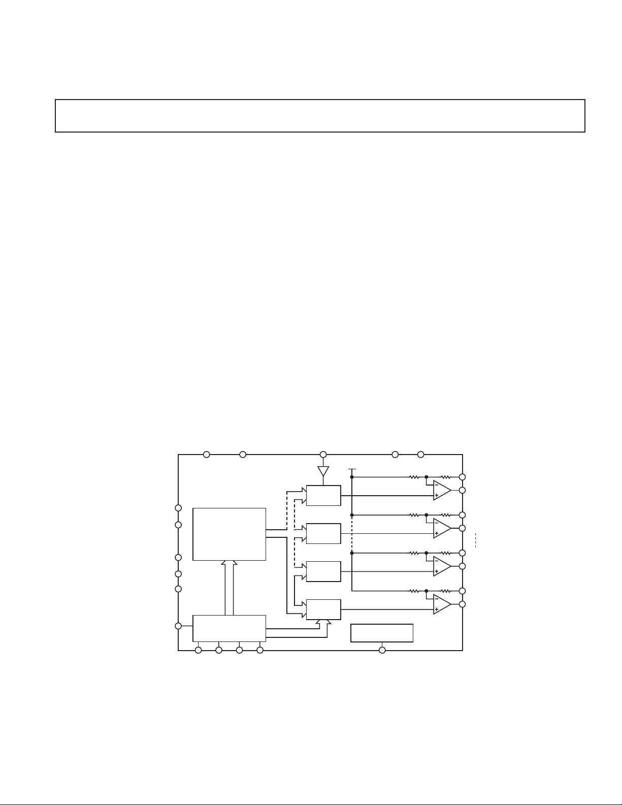
FUNCTIONAL BLOCK DIAGRAM
with 14-Bit Increment Mode
AD5516
GENERAL DESCRIPTION
The AD5516 is a 16-channel, 12-bit voltage-output DAC. The
selected DAC register is written to via the 3-wire serial interface.
DAC selection is accomplished via address bits A3–A0. 14-bit
resolution can be achieved by fine adjustment in Increment/
Decrement Mode (Mode 2). The serial interface operates at
clock rates up to 20 MHz and is compatible with standard SPI,
MICROWIRE, and DSP interface standards. The output voltage range is fixed at ±2.5 V (AD5516-1), ±5 V (AD5516-2),
and ± 10 V (AD5516-3). Access to the feedback resistor in each
channel is provided via R
The device is operated with AV
5.25 V, V
= –4.75 V to –12 V, and V
SS
and requires a stable 3 V reference on REF_IN.
PRODUCT HIGHLIGHTS
1. Sixteen 12-bit DACs in one package, guaranteed monotonic
2. Available in a 74-lead LFBGA package with a body size of
12 mm ⴛ 12 mm
0 to RFB15 pins.
FB
= 5 V ± 5%, DVCC = 2.7 V to
CC
= +4.75 V to +12 V
DD
*
DV
AV
CC
CC
AD5516
RESET
BUSY
DACGND
AGND
DGND
DCEN
ANALOG
CALIBRATION
LOOP
MODE1
INTERFACE
CONTROL
LOGIC
SCLK DIND
12-BIT BUS
SYNC
OUT
MODE2
7-BIT BUS
*Protected by U.S. Patent No. 5,969,657; other patents pending
SPI and QSPI are trademarks of Motorola, Inc.
MICROWIRE is a trademark of National Semiconductor Corporation.
REV. 0
Information furnished by Analog Devices is believed to be accurate and
reliable. However, no responsibility is assumed by Analog Devices for its
use, nor for any infringements of patents or other rights of third parties that
may result from its use. No license is granted by implication or otherwise
under any patent or patent rights of Analog Devices.
LOGIC
PD
V
DDVSS
R
OFFS
R
OFFS
R
OFFS
R
OFFS
R
FB
RFB0
V
0
OUT
R
FB
RFB1
1
V
OUT
R
FB
R
FB
14
R
FB
14
V
OUT
15
R
FB
V
15
OUT
REF_IN
V
BIAS
DAC
DAC
DAC
DAC
POWER-DOWN
One Technology Way, P.O. Box 9106, Norwood, MA 02062-9106, U.S.A.
Tel: 781/329-4700 www.analog.com
Fax: 781/326-8703 © Analog Devices, Inc., 2002

(VDD = +4.75 V to +13.2 V, VSS = –4.75 V to –13.2 V; AVCC = 4.75 V to 5.25 V; DVCC =
AD5516
All specifications T
Parameter
–SPECIFICATIONS
to T
1
MIN
unless otherwise noted.)
MAX
DAC DC PERFORMANCE
Resolution 12 Bits
Integral Nonlinearity (INL) ± 2 LSB max Mode 1
Differential Nonlinearity (DNL) –1/+1.3 LSB max ±0.5 LSB typ, Monotonic; Mode 1
Increment/Decrement Step-Size ± 0.25 LSB typ Monotonic; Mode 2 Only
Bipolar Zero Error ± 7 LSB max
Positive Full-Scale Error ± 10 LSB max
Negative Full-Scale Error ± 10 LSB max
VOLTAGE REFERENCE
REF_IN
Nominal Input Voltage 3 V
Input Voltage Range
3
Input Current ± 1 µA max < 1 nA typ
ANALOG OUTPUTS (V
Output Temperature Coefficient
DC Output Impedance
Output Range
5
OUT
3
0–15)
3, 4
AD5516-1 ± 2.5 V typ
AD5516-2 ± 5 V typ
AD5516-3 ± 10 V typ
Resistive Load
Capacitive Load
Short-Circuit Current
DC Power-Supply Rejection Ratio
DC Crosstalk
DIGITAL INPUTS
3, 6
3, 6
3
3
3
3
Input Current ± 10 µA max ±5 µA typ
Input Low Voltage 0.8 V max DV
Input High Voltage 2.4 V min DVCC = 5 V ± 5%
Input Hysteresis (SCLK and SYNC) 150 mV typ
Input Capacitance 10 pF max 5 pF typ
3
DIGITAL OUTPUTS (BUSY, D
OUT
)
Output Low Voltage, DVCC = 5 V 0.4 V max Sinking 200 µA
Output High Voltage, DVCC = 5 V 4 V min Sourcing 200 µA
Output Low Voltage, DVCC = 3 V 0.4 V max Sinking 200 µA
Output High Voltage, DVCC = 3 V 2.4 V min Sourcing 200 µA
High Impedance Leakage Current (D
High Impedance Output Capacitance (D
only) ± 1 µA max DCEN = 0
OUT
only) 5 pF typ DCEN = 0
OUT
POWER REQUIREMENTS
Power Supply Voltages
V
DD
V
SS
AV
CC
DV
CC
Power Supply Currents
I
DD
I
SS
AI
CC
DI
CC
Power-Down Currents
I
DD
I
SS
AI
CC
DI
CC
Power Dissipation
NOTES
1
See Terminology section.
2
A Version: Industrial temperature range –40°C to +85°C; typical at +25°C.
3
Guaranteed by design and characterization; not production tested.
4
AD780 as reference for the AD5516.
5
Output range is restricted from V
6
Ensure that you do not exceed T
7
Outputs unloaded.
Specifications subject to change without notice.
7
7
7
+ 2 V to V
SS
. See Absolute Maximum Ratings section.
J (MAX)
– 2 V. Output span varies with reference voltage and is functional down to 2 V.
DD
2.7 V to 5.25 V; AGND = DGND = DACGND = 0 V; REF_IN = 3 V; All outputs unloaded.
A Version
2.875/3.125 V min/max
10 ppm/°C typ of FSR
0.5 Ω typ
5kΩ min
200 pF
7 mA typ
–85 dB typ VDD = +12 V ± 5%, VSS = –12 V ± 5%
120 µV max
0.4 V max DVCC = 3 V ± 10%
2 V min DVCC = 3 V ± 10%
+4.75/+15.75 V min/max
–4.75/–15.75 V min/max
4.75/5.25 V min/max
2.7/5.25 V min/max
5 mA max 3.5 mA typ. All Channels Full-Scale
5 mA max 3.5 mA typ. All Channels Full-Scale
17 mA max 13 mA typ
1.5 mA max 1 mA typ
2 µA max 200 nA typ
3 µA max 200 nA typ
2 µA max 200 nA typ
2 µA max 200 nA typ
105 mW typ VDD= +5 V, VSS= –5 V
2
Unit Conditions/Comments
= 5 V ± 5%
CC
–2–
REV. 0

AD5516
(VDD = +4.75 V to +13.2 V, VSS = –4.75 V to –13.2 V; AVCC = 4.75 V to 5.25 V; DVCC = 2.7 V to 5.25 V; AGND = DGND
AC CHARACTERISTICS
Parameter
Output Voltage Settling Time (Mode 1)
Output Voltage Settling Time (Mode 2)
1, 2
= DACGND = 0 V; REF_IN = 3 V; All outputs unloaded. All specifications T
A Version
4
4
32 s max 100 pF, 5 kΩ Load Full-Scale Change
2.5 s max 100 pF, 5 kΩ Load, 1 Code Increment
3
Unit Conditions/Comments
Slew Rate 0.85 V/s typ
Digital-to-Analog Glitch Impulse 1 nV-s typ 1 LSB Change around Major Carry
Digital Crosstalk 5 nV-s typ
Analog Crosstalk AD5516-1 10 nV-s typ
Digital Feedthrough 1 nV-s typ
Output Noise Spectral Density @ 1 kHz 150 nV/(Hz)
NOTES
1
See Terminology section.
2
Guaranteed by design and characterization; not production tested.
3
A version: Industrial temperature range –40°C to +85°C.
4
Timed from the end of a write sequence.
Specifications subject to change without notice.
1/2
typ AD5516-1
(VDD = +4.75 V to +13.2 V, VSS = – 4.75 V to –13.2 V; AVCC = 4.75 V to 5.25 V; DVCC = 2.7 V to 5.25 V;
TIMING CHARACTERISTICS
Parameter
f
UPDATE1
f
UPDATE2
f
CLKIN
t
1
t
2
t
3
t
4
t
5
t
6
t
7
t
7MODE2
t
8MODE1
t
9MODE2
t
10
4
t
11
t
12
NOTES
1
See Timing Diagrams in Figures 1 and 2.
2
Guaranteed by design and characterization; not production tested.
3
All input signals are specified with tr = tf = 5 ns (10% to 90% of DVCC) and timed from a voltage level of (VIL + VIH)/2.
4
This is measured with the load circuit of Figure 3.
Specifications subject to change without notice.
1, 2, 3
Limit at T
(A Version) Unit Conditions/Comments
32 kHz max DAC Update Rate (Mode 1)
750 kHz max DAC Update Rate (Mode 2)
20 MHz max SCLK Frequency
20 ns min SCLK High Pulsewidth
20 ns min SCLK Low Pulsewidth
15 ns min SYNC Falling Edge to SCLK Falling Edge Setup Time
5 ns min DIN Setup Time
5 ns min DIN Hold Time
0 ns min SCLK Falling Edge to SYNC Rising Edge
10 ns min Minimum SYNC High Time (Standalone Mode)
400 ns min Minimum SYNC High Time (Daisy-Chain Mode)
10 ns min BUSY Rising Edge to SYNC Falling Edge
200 ns min 18th SCLK Falling Edge to SYNC Falling Edge (Standalone Mode)
10 ns min SYNC Rising Edge to SCLK Rising Edge (Daisy-Chain Mode)
20 ns max SCLK Rising Edge to D
20 ns min RESET Pulsewidth
MIN
, T
AGND = DGND = DACGND = 0 V. All specifications T
MAX
to T
MIN
MAX
Valid (Daisy-Chain Mode)
OUT
to T
MIN
unless otherwise noted.)
MAX
unless otherwise noted.)
–3–
AD5516
SERIAL INTERFACE TIMING DIAGRAMS
SCLK
SYNC
DIN
BUSY
RESET
SCLK
SYNC
D
1 2 17 18
t
MODE1
8
t
t
7
3
t
4
BIT 17 BIT 0
t
2
t
5
t
1
t
6
t
MODE2
LSBMSB
9
t
12
Figure 1. Serial Interface Timing Diagram
t
t
MODE2
7
IN
3
t
4
BIT 17 BIT 0 BIT 17 BIT 0
t
2
t
5
t
1
LSBMSB
t
10
t
6
D
OUT
BUSY
t
MODE1
8
INPUT WORD FOR DEVICE N
t
11
BIT 17 BIT 0
UNDEFINED INPUT WORD FOR DEVICE N
Figure 2. Daisy-Chaining Timing Diagram
200A
TO OUTPUT
PIN
C
L
50pF
200A
Figure 3. Load Circuit for D
I
OL
I
OH
Timing Specifications
OUT
INPUT WORD FOR DEVICE N+1
1.6V
–4–
REV. 0
AD5516
ABSOLUTE MAXIMUM RATINGS
(TA = 25°C unless otherwise noted.)
VDD to AGND . . . . . . . . . . . . . . . . . . . . . . . . –0.3 V to +17 V
to AGND . . . . . . . . . . . . . . . . . . . . . . . . +0.3 V to –17 V
V
SS
AV
to AGND, DACGND . . . . . . . . . . . . . . –0.3 V to +7 V
CC
DV
to DGND . . . . . . . . . . . . . . . . . . . . . . . –0.3 V to +7 V
CC
Digital Inputs to DGND . . . . . . . . . . –0.3 V to DV
Digital Outputs to DGND . . . . . . . . . –0.3 V to DV
REF_IN to AGND, DACGND . . . . . –0.3 V to AV
0–15 to AGND . . . . . . . . . . . . V
V
OUT
AGND to DGND . . . . . . . . . . . . . . . . . . . . –0.3 V to +0.3 V
R
0–15 to AGND . . . . . . . . . . . . V
FB
1, 2
CC
CC
– 0.3 V to V
SS
– 0.3 V to VDD+ 0.3 V
SS
CC
DD
+ 0.3 V
+ 0.3 V
+ 0.3 V
+ 0.3 V
Storage Temperature Range . . . . . . . . . . . . –65°C to +150°C
Junction Temperature (T
74-Lead LFBGA Package,
) . . . . . . . . . . . . . . . . . . . 150°C
J MAX
Thermal Impedance . . 41°C/W
JA
Reflow Soldering
Peak Temperature . . . . . . . . . . . . . . . . . . . . . . . . . . . 220°C
Time at Peak Temperature . . . . . . . . . . . . .10 sec to 40 sec
NOTES
1
Stresses above those listed under Absolute Maximum Ratings may cause permanent
damage to the device. This is a stress rating only; functional operation of the device
at these or any other conditions above those listed in the operational sections of this
specification is not implied. Exposure to absolute maximum rating conditions for
extended periods may affect device reliability.
2
Transient currents of up to 100 mA will not cause SCR latch-up.
Operating Temperature Range, Industrial . . . . . –40°C to +85°C
ORDERING GUIDE
Model Function Output Voltage Span Package Option
AD5516ABC-1 16 DACs ± 2.5 V 74-Lead LFBGA
AD5516ABC-2 16 DACs ± 5 V 74-Lead LFBGA
AD5516ABC-3 16 DACs ± 10 V 74-Lead LFBGA
CAUTION
ESD (electrostatic discharge) sensitive device. Electrostatic charges as high as 4000 V readily
accumulate on the human body and test equipment and can discharge without detection. Although
the AD5516 features proprietary ESD protection circuitry, permanent damage may occur on
devices subjected to high-energy electrostatic discharges. Therefore, proper ESD precautions are
recommended to avoid performance degradation or loss of functionality.
WARNING!
ESD SENSITIVE DEVICE
REV. 0
–5–

AD5516
PIN CONFIGURATION
1110987654321
A
B
C
D
E
F
G
H
J
K
LL
TOP VIEW
A
B
C
D
E
F
G
H
J
K
1110987654321
74-LEAD LFBGA BALL CONFIGURATION
LFBGA Ball LFBGA Ball LFBGA Ball LFBGA Ball LFBGA Ball
Number Name Number Name Number Name Number Name Number Name
A1 NC
A2 NC
A3 RESET
A4 BUSY
A5 DGND
A6 DV
A7 D
A8 D
CC
OUT
IN
A9 SYNC
A10 NC
A11 NC
B1 NC
B2 NC
B3 NC
B4 DCEN
NC = Not Internally Connected
B5 DGND
B6 DGND
B7 NC
B8 NC
B9 SCLK
B10 NC
B11 REF_IN
C1 V
OUT
0
C2 DACGND
C6 NC
C10 AV
CC
1
C11 NC
D1 R
FB
0
D2 DACGND
D10 AVCC2
D11 NC
E1 V
OUT
1
E2 NC
E10 AGND1
E11 PD
F1 V
F2 R
OUT
FB
2
1
F10 AGND2
F11 R
G1 R
G2 R
G10 V
G11 R
H1 V
H2 V
FB
FB
FB
OUT
FB
OUT
OUT
14
2
15
14
13
3
15
H10 V
H11 V
J1 R
J2 V
OUT
OUT
FB
OUT
J6 NC
J10 R
J11 R
K1 R
K2 V
K3 R
FB
FB
FB
OUT
FB
K4 NC
K5 V
K6 V
K7 V
K8 V
SS
SS
OUT
OUT
3
12
11
4
5
2
1
13
12
14
5
10
9
K9 RFB10
K10 R
K11 V
FB
OUT
9
L1 NC
L2 V
L3 R
L4 V
OUT
FB
OUT
6
L5 NC
L6 VDD2
L7 V
L8 R
L9 V
L10 R
DD
FB
OUT
FB
1
7
8
L11 NC
11
6
7
8
PIN FUNCTION DESCRIPTIONS
Mnemonic Function
AGND (1–2) Analog GND pins
AV
(1–2) Analog supply pins. Voltage range from +4.75 V to +5.25 V.
CC
V
(1–2) VDD supply pins. Voltage range from +4.75 V to +15.75 V.
DD
V
(1–2) VSS supply pins. Voltage range from –4.75 V to –15.75 V.
SS
DGND Digital GND pins
DV
CC
Digital supply pin. Voltage range from 2.7 V to 5.25 V.
DACGND Reference GND supply for all 16 DACs.
REF_IN Reference input voltage for all 16 DACs. The recommended value of REF_IN is 3 V.
V
(0–15) Analog output voltages from the 16 DAC channels.
OUT
R
(0–15) Feedback resistors. For nominal output voltage range connect each RFB to its corresponding V
FB
OUT
.
SYNC Active low input. This is the frame synchronization signal for the serial interface. While SYNC is low, data is
transferred in on the falling edge of SCLK.
SCLK Serial clock input. Data is clocked into the shift register on the falling edge of SCLK. This operates at clock
speeds up to 20 MHz.
D
IN
Serial data input. Data must be valid on the falling edge of SCLK.
–6–
REV. 0

Mnemonic Function
AD5516
PIN FUNCTION DESCRIPTIONS (continued)
D
OUT
Serial data output. D
data in the shift register for diagnostic purposes. Data is clocked out on D
can be used for daisy-chaining a number of devices together or for reading back the
OUT
OUT
on the rising edge of SCLK and is
valid on the falling edge of SCLK.
1
DCEN
RESET
1
PD
2
Active high control input. This pin is tied high to enable daisy-chain mode.
Active low control input. This resets all DAC registers to power-on value.
Active high control input. All DACs go into power-down mode when this pin is high. The DAC outputs go into
a high-impedance state.
BUSY Active low output. This signal tells the user that the analog calibration loop is active. It goes low during
conversion. The duration of the pulse on BUSY determines the maximum DAC update rate, f
UPDATE
. Further
writes to the AD5516 are ignored while BUSY is active.
NOTES
1
Internal pull-down device on this logic input. Therefore it can be left floating and will default to a logic low condition.
2
Internal pull-up device on this logic input. Therefore it can be left floating and will default to a logic high condition.
TERMINOLOGY
Integral Nonlinearity (INL)
This is a measure of the maximum deviation from a straight line
passing through the endpoints of the DAC transfer function. It is
expressed in LSBs.
Differential Nonlinearity (DNL)
Differential nonlinearity (DNL) is the difference between the
measured change and the ideal 1 LSB change between any two
adjacent codes. A specified DNL of –1 LSB maximum ensures
monotonicity.
Bipolar Zero Error
Bipolar zero error is the deviation of the DAC output from the ideal
midscale of 0 V. It is measured with 10...00 loaded to the DAC.
It is expressed in LSBs.
Positive Full-Scale Error
This is the error in the DAC output voltage with all 1s loaded to
the DAC. Ideally the DAC output voltage, with all 1s loaded to the
DAC registers, should be 2.5 V – 1 LSB (AD5516-1), 5 V – 1 LSB
(AD5516-2), and 10 V – 1 LSB (AD5516-3). It is expressed in LSBs.
Negative Full-Scale Error
This is the error in the DAC output voltage with all 0s loaded to the
DAC. Ideally the DAC output voltage, with all 0s loaded to the
DAC registers, should be –2.5 V (AD5516-1), –5 V (AD5516-2),
and –10 V (AD5516-3). It is expressed in LSBs.
Output Temperature Coefficient
This is a measure of the change in analog output with changes in
temperature. It is expressed in ppm/°C of FSR.
DC Power Supply Rejection Ratio
DC power supply rejection ratio (PSRR) is a measure of the change
in analog output for a change in supply voltage (V
It is expressed in dBs. V
and VSS are varied ± 5%.
DD
and VSS).
DD
DC Crosstalk
This is the dc change in the output level of one DAC at midscale
in response to a full-scale code change (all 0s to all 1s and vice
versa) and output change of another DAC. It is expressed in mV.
Output Settling Time
This is the time taken from when the last data bit is clocked into
the DAC until the output has settled to within ±0.5 LSB of its
final value (see TPC 7).
Digital-to-Analog Glitch Impulse
This is the area of the glitch injected into the analog output when
the code in the DAC register changes state. It is specified as the
area of the glitch in nV-secs when the digital code is changed by
1 LSB at the major carry transition (011...11 to 100...00 or
100...00 to 011...11).
Digital Crosstalk
This is the glitch impulse transferred to the output of one DAC at
midscale while a full-scale code change (all 1s to all 0s and vice
versa) is being written to another DAC. It is expressed in nV-secs.
Analog Crosstalk
This is the area of the glitch transferred to the output (V
one DAC due to a full-scale change in the output (V
OUT
OUT
) of
another DAC. The area of the glitch is expressed in nV-secs.
Digital Feedthrough
This is a measure of the impulse injected into the analog outputs
from the digital control inputs when the part is not being written
to, i.e., SYNC is high. It is specified in nV-secs and measured
with a worst-case change on the digital input pins, e.g., from all
0s to all 1s and vice versa.
Output Noise Spectral Density
This is a measure of internally generated random noise. Random
noise is characterized as a spectral density (voltage per root Hertz).
It is measured in nV/(Hz)
1/2
.
) of
REV. 0
–7–

CURRENT – mA
V
OUT
– V
–6
0.002
–4 –202 64
MIDSCALE
REF_IN = 3V
T
A
= 25ⴗC
0.0
–0.002
–0.004
–0.006
–0.008
–0.01
0.004
0.006
0.008
0.01
8–8
–Typical Performance CharacteristicsAD5516
1.0
REF_IN = 3V
= 25ⴗC
T
0.8
A
0.6
0.4
0.2
0
–0.2
DNL ERROR – LSB
–0.4
–0.6
–0.8
–1.0
1000 2000 3000 40000
TPC 1. Typical DNL Plot
3
REF_IN = 3V
2
1
BIPOLAR ZERO ERROR
0
ERROR – LSB
–1
–2
–3
–40
NEGATIVE FS ERROR
POSITIVE FS ERROR
–20 0 20 40 80
TEMPERATURE – ⴗC
DAC CODE
–0.2
INL ERROR – LSB
–0.4
–0.6
–0.8
–1.0
1.0
REF_IN = 3V
= 25ⴗC
T
0.8
A
0.6
0.4
0.2
0
0
1000 2000 3000 4000
DAC CODE
TPC 2. Typical INL Plot
2.0
REF_IN = 3V
1.5
–0.5
ERROR – LSB
–1.0
–1.5
–2.0
1.0
0.5
0
–20 0 20 40 80
–40
TEMPERATURE – ⴗC
INL
+VE
DNL
–VE
DNL
60
TPC 3. Typical INL Error and DNL
Error vs. Temperature
0.003
AV
= +12V
DD
= –12V
AV
SS
0.002
0.001
– V
0
OUT
V
–0.001
–0.002
60
–0.003
–40
= 3V
REF_IN
MIDSCALE LOADED
–20 0 20 40 80
TEMPERATURE – ⴗC
60
TPC 4. Bipolar Zero Error and
Full-Scale Error vs. Temperature
3.0
TA = 25ⴗC
REF_IN = 3V
2.0
1.0
– V
0
OUT
V
–1.0
–2.0
–3.0
TIME BASE = 2.5s/DIV
TPC 7. Full-Scale Settling Time
TPC 5. V
vs. Temperature
OUT
TPC 6. V
Source and Sink
OUT
Capability
= 25ⴗC
T
A
REF_IN = 3V
PD
V
OUT
5V/DIV
2V/DIV
2s/DIV
TPC 8. Exiting Power-Down to
Full Scale
–8–
–0.029
TA = 25ⴗC
REF_IN = 3V
–0.030
–0.031
–0.032
–0.033
OLD
VA LU E
CALIBRATION TIME
2.5s/DIV
5V
0V
TPC 9. Major Code Transition
Glitch Impulse
NEW
VA LU E
BUSY
REV. 0

AD5516
450
400
350
300
250
200
FREQUENCY
150
100
50
0
TPC 10. V
V
– V
OUT
Repeatability; Program-
OUT
2.48992.48962.4893
ming the Same Code Multiple Times
30
REF_IN = 3V
= 25ⴗC
T
A
20
40
REF_IN = 3V
= 25ⴗC
T
A
20
FREQUENCY – %
0
–10 0 10
LSBs
TPC 11. Bipolar Error Distribution
2.5
2.0
1.5
REF_IN = 3V
= 25ⴗC
T
A
40
REF_IN = 3V
TA = 25ⴗC
20
FREQUENCY – %
0
–10 0 10
LSBs
TPC 12. Positive Full-Scale
Error Distribution
10
FREQUENCY – %
0
–10 0 10
LSBs
TPC 13. Negative Full-Scale Error Distribution
1.0
ERROR – LSB
0.5
0
0 20 40 60 80 100 120
STEP SIZE
130
TPC 14. Increment Step vs. Accuracy
REV. 0
–9–

AD5516
FUNCTIONAL DESCRIPTION
The AD5516 consists of sixteen 12-bit DACs in a single package.
A single reference input pin (REF_IN) is used to provide a 3 V
reference for all 16 DACs. To update a DAC’s output voltage
the required DAC is addressed via the 3-wire serial interface.
Once the serial write is complete, the selected DAC converts the
code into an output voltage. The output amplifiers translate the
DAC output range to give the appropriate voltage range (±2.5 V,
± 5 V, or ± 10 V) at output pins V
OUT
0 to V
OUT
15.
The AD5516 uses a self-calibrating architecture to achieve
12-bit performance. The calibration routine servos to select the
appropriate voltage level on an internal 14-bit resolution DAC.
Noise during the calibration (
BUSY
low period) can result in
the selection of a voltage within a ±0.25 LSB band around the
normal selected voltage. See TPC 10.
It is essential to minimize noise on REFIN for optimal performance. The AD780’s specified decoupling makes it the ideal
reference to drive the AD5516.
On power-on, all DACs power up to a reset value (see RESET
section).
DIGITAL-TO-ANALOG SECTION
The architecture of each DAC channel consists of a resistorstring DAC followed by an output buffer amplifier. The voltage
at the REF_IN Pin provides the reference voltage for the corresponding DAC. The input coding to the DAC is offset binary;
this results in ideal DAC output voltages as follows:
AD5516-1
AD5516-2
AD5516-3
×××××225
V
DAC
V
DAC
V
DAC
REF IN
=
=
=
32
VDV
×××
REF IN
32
VDV
×××
REF IN
32
.
__
N
.
__
N
×
.
__
N
×
REF IN
–
225
–
425
–
3
REF IN
3
REF IN
3
25
.
×425
×825
.
.
VDV
Where:
D = decimal equivalent of the binary code that is loaded to
the DAC register, i.e., 0–4096
N = DAC resolution = 12
Table I illustrates ideal analog output versus DAC code.
Table I. DAC Register Contents AD5516-1
MSB LSB Analog Output, V
1111 1111 1111 V
× 2.5/3 – 1 LSB
REF_IN
OUT
1000 0000 0000 0 V
0000 0000 0000 –V
REF_IN
× 2.5/3
MODES OF OPERATION
The AD5516 has two modes of operation.
Mode 1 (MODE bits = 00): The user programs a 12-bit data
word to one of 16 channels via the serial interface. This word is
loaded into the addressed DAC register and is then converted
into an analog output voltage. During conversion the BUSY
output is low and all SCLK pulses are ignored. At the end of a
conversion BUSY goes high indicating that the update of the
addressed DAC is complete. It is recommended that SCLK is
not pulsed while BUSY is low. Mode 1 conversion takes 25 µs typ.
Mode 2 (MODE bits = 01 or 10): Mode 2 operation allows the
user to increment or decrement the DAC output in 0.25 LSB steps,
resulting in a 14-bit monotonic DAC. The amount by which the
DAC output is incremented or decremented is determined by
Mode 2 bits DB6–DB0, e.g., for a 0.25 LSB increment/decrement
DB6...DB0 = 0000001, while for a 2.5 LSB increment/decrement,
DB6...DB0 = 0001010. The MODE bits determine whether the
DAC data is incremented (01) or decremented (10). The maximum
amount that the user is allowed to increment or decrement the DAC
output is 127 steps of 0.25 LSB, i.e., DB6...DB0 = 1111111.
Mode 2 update takes approximately 1 µs. The Mode 2 feature
allows increased resolution but overall increment/decrement accuracy varies with increment/decrement step as shown in TPC 14.
Mode 2 is useful in applications where greater resolution is
required, for example, in servo applications requiring fine-tune
to 14-bit resolution.
MSB LSB
0 0 A3 A2 A1 A0 DB11 DB10 DB9 DB8 DB7 DB6 DB5 DB4 DB3 DB2 DB1 DB0
MODE
BITS
ADDRESS
BITS
DATA
BITS
Figure 4. Mode 1 Data Format
MSB LSB
0 1 A3 A2 A1 A0 0 0 0 0 0 DB6 DB5 DB4 DB3 DB2 DB1 DB0
MODE
BITS
MSB LSB
1 0 A3 A2 A1 A0 0 0 0 0 0 DB6 DB5 DB4 DB3 DB2 DB1 DB0
MODE
BITS
ADDRESS
BITS
ADDRESS
BITS
7 INCREMENT
BITS
7 DECREMENT
BITS
Figure 5. Mode 2 Data Format
–10–
REV. 0

AD5516
The user must allow 200 ns (min) between two consecutive
Mode 2 writes in standalone mode and 400 ns (min) between
two consecutive Mode 2 writes in daisy-chain mode.
See Figures 4 and 5 for Mode 1 and Mode 2 data formats.
When MODE bits = 11, the device is in No Operation mode.
This may be useful in daisy-chain applications where the user
does not wish to change the settings of the DACs. Simply write
11 to the MODE bits and the following address and data bits
will be ignored.
SERIAL INTERFACE
The AD5516 has a 3-wire interface that is compatible with SPI/
QSPI/MICROWIRE and DSP interface standards. Data is written
to the device in 18-bit words. This 18-bit word consists of two
mode bits, four address bits, and 12 data bits as shown in Figure 4.
The serial interface works with both a continuous and burst
clock. The first falling edge of SYNC resets a counter that counts
the number of serial clocks to ensure the correct number of bits
are shifted in and out of the serial shift registers. Any further
edges on SYNC are ignored until the correct number of bits are
shifted in or out. In order for another serial transfer to take
place, the counter must be reset by the falling edge of SYNC.
A3–A0
Four address bits (A3 = MSB Address, A0 = LSB). These are
used to address one of 16 DACs.
Table II. Selected DAC
A3 A2 A1 A0 Selected DAC
0 0 0 0 DAC 0
0 0 0 1 DAC 1
::::
1 1 1 1 DAC 15
DB11–DB0
These are used to write a 12-bit word into the addressed DAC
register. Figures 1 and 2 show the timing diagram for a write
cycle to the AD5516.
SYNC FUNCTION
In both standalone and daisy-chain modes, SYNC is an edgetriggered input that acts as a frame synchronization signal and
chip enable. Data can only be transferred into the device while
SYNC is low. To start the serial data transfer, SYNC should be
taken low observing the minimum SYNC falling to SCLK falling
edge setup time, t
Standalone Mode (DCEN = 0)
.
3
After SYNC goes low, serial data will be shifted into the device’s
input shift register on the falling edges of SCLK for 18 clock
pulses. After the falling edge of the 18th SCLK pulse, data will
automatically be transferred from the input shift register to the
addressed DAC.
SYNC must be taken high and low again for further serial data
transfer. SYNC may be taken high after the falling edge of the
18th SCLK pulse, observing the minimum SCLK falling edge
to SYNC rising edge time, t
. If SYNC is taken high before the
6
18th falling edge of SCLK, the data transfer will be aborted and
the addressed DAC will not be updated. See the timing diagram
in Figure 1.
Daisy-Chain Mode (DCEN = 1)
n daisy-chain mode, the internal gating on SCLK is disabled.
I
The SCLK is continuously applied to the input shift register
when SYNC is low. If more than 18 clock pulses are applied,
the data ripples out of the shift register and appears on the D
OUT
line. This data is clocked out on the rising edge of SCLK and is
valid on the falling edge. By connecting this line to the D
IN
input on the next device in the chain, a multidevice interface is
constructed. Eighteen clock pulses are required for each device
in the system. Therefore, the total number of clock cycles must
equal 18N where N is the total number of devices in the chain.
See the timing diagram in Figure 2.
When the serial transfer to all devices is complete, SYNC should
be taken high. This prevents any further data being clocked into the
input shift register. A burst clock containing the exact number of
clock cycles may be used and SYNC taken high some time later.
After the rising edge of SYNC, data is automatically transferred
from each device’s input shift register to the addressed DAC.
RESET Function
The RESET function on the AD5516 can be used to reset all
nodes on this device to their power-on reset condition. This is
implemented by applying a low-going pulse of minimum 20 ns
to the RESET Pin on the device.
Table III. Typical Power-ON Values
Device Output Voltage
AD5516-1 –0.073 V
AD5516-2 –0.183 V
AD5516-3 –0.391 V
BUSY Output
During conversion, the BUSY output is low and all SCLK
pulses are ignored. At the end of a conversion, BUSY goes high
indicating that the update of the addressed DAC is complete. It
is recommended that SCLK is not pulsed while BUSY is low.
MICROPROCESSOR INTERFACING
The AD5516 is controlled via a versatile 3-wire serial interface
that is compatible with a number of microprocessors and DSPs.
AD5516 to ADSP-2106x SHARC DSP Interface
The ADSP-2106x SHARC DSPs are easily interfaced to the
AD5516 without the need for extra logic.
The AD5516 expects a t
(SYNC falling edge to SCLK falling
3
edge setup time) of 15 ns min. Consult the ADSP-2106x User
Manual for information on clock and frame sync frequencies for
the SPORT register and contents of the TDIV, RDIV registers.
REV. 0
–11–

AD5516
A data transfer is initiated by writing a word to the TX register
after the SPORT has been enabled. In write sequences data is
clocked out on each rising edge of the DSP’s serial clock and
clocked into the AD5516 on the falling edge of its SCLK. The
SPORT transmit control register should be set up as follows:
DTYPE = 00, Right Justify Data
ICLK = 1, Internal Serial Clock
TFSR = 1, Frame Every Word
INTF = 1, Internal Frame Sync
LTFS = 1, Active Low Frame Sync Signal
LAFS = 0, Early Frame Sync
SENDN = 0, Data Transmitted MSB First
SLEN = 10011, 18-Bit Data Words (SLEN = Serial Word)
Figure 6 shows the connection diagram.
AD5516*
SYNC
D
IN
SCLK
*ADDITIONAL PINS OMITTED FOR CLARITY
ADSP-2106x*
TFS
DT
SCLK
Figure 6. AD5516 to ADSP-2106x Interface
AD5516 to MC68HC11
The serial peripheral interface (SPI) on the MC68HC11 is
configured for master mode (MSTR = 1), clock polarity bit
(CPOL) = 0, and the clock phase bit (CPHA) = 1. The SPI is
configured by writing to the SPI control register (SPCR)—see
the 68HC11 User Manual. SCK of the 68HC11 drives the SCLK
of the AD5516, the MOSI output drives the serial data line
) of the AD5516. The SYNC signal is derived from a port
(D
IN
line (PC7). When data is being transmitted to the AD5516, the
SYNC line is taken low (PC7). Data appearing on the MOSI
output is valid on the falling edge of SCK. Serial data from the
68HC11 is transmitted in 8-bit bytes with only eight falling
clock edges occurring in the transmit cycle. Data is transmitted
MSB first. In order to transmit 18 data bits, it is important to
left justify the data in the SPDR register. PC7 must be pulled
low to start a transfer and taken high and low again before any
further read/write cycles can take place. A connection diagram is
shown in Figure 7.
AD5516*
SYNC
SCLK
D
IN
*ADDITIONAL PINS OMITTED FOR CLARITY
MC68HC11*
PC7
SCK
MOSI
Figure 7. AD5516 to MC68HC11 Interface
AD5516 to PIC16C6x/7x
The PIC16C6x/7x synchronous serial port (SSP) is configured
as an SPI master with the clock polarity bit (CKP) = 0. This is
done by writing to the synchronous serial port control register
(SSPCON). See user PIC16/17 Microcontroller User Manual.
In this example, I/O port RA1 is being used to provide a SYNC
signal and enable the serial port of the AD5516. This microcontroller transfers only eight bits of data during each serial transfer
operation; therefore, three consecutive write operations are
required. Figure 8 shows the connection diagram.
AD5516*
SCLK
D
IN
SYNC
*ADDITIONAL PINS OMITTED FOR CLARITY
PIC16C6x/7x*
SCK/RC3
SDI/RC4
RA1
Figure 8. AD5516 to PIC16C6x/7x Interface
AD5516 to 8051
A serial interface between the AD5516 and the 80C51/80L51
microcontroller is shown in Figure 9. The AD5516 requires a
clock synchronized to the serial data. The 8051 serial interface
must therefore be operated in Mode 0. TxD of the microcontroller drives the SCLK of the AD5516, while RxD drives the
serial data line. P3.3 is a bit programmable pin on the serial port
that is used to drive SYNC. The 80C51/80L51 provides the
LSB first, while the AD5516 expects MSB of the 18-bit word
first. Care should be taken to ensure the transmit routine takes
this into account.
AD5516*
SCLK
D
IN
SYNC
*ADDITIONAL PINS OMITTED FOR CLARITY
8051*
TxD
RxD
P1.1
Figure 9. AD5516 to 8051 Interface
When data is to be transmitted to the DAC, P3.3 is taken
low. Data on RxD is valid on the falling edge of TxD, so the
clock must be inverted as the AD5516 clocks data into the
input shift register on the rising edge of the serial clock. The
80C51/80L51 transmits its data in 8-bit bytes with only eight
falling clock edges occurring in the transmit cycle. As the DAC
requires an 18-bit word, P3.3 must be left low after the first eight
bits are transferred, and brought high after the complete 18 bits
have been transferred. DOUT may be tied to RxD for data verification purposes when the device is in daisy-chain mode.
–12–
REV. 0

AD5516
APPLICATION CIRCUITS
The AD5516 is suited for use in many applications, such as level
setting, optical, industrial systems, and automatic test applications. In level setting and servo applications where a fine-tune
adjust is required, the Mode 2 function increases resolution.
The following figures show the AD5516 used in some potential
applications.
AD5516 in a Typical ATE System
The AD5516 is ideally suited for the level setting function in
automatic test equipment. A number of DACs are required to
control pin drivers, comparators, active loads, parametric measurement units, and signal timing. Figure 10 shows the AD5516
in such a system.
STORED
DATA AND
INHIBIT
PATTERN
PERIOD
GENERATION
AND
DELAY
TIMING
DACs
DAC
DAC
DAC
FORMATTER
COMPARE
REGISTER
SYSTEM BUS
ACTIVE
LOAD
DRIVER
PARAMETRIC
MEASUREMENT
UNIT
DAC
DAC
COMPARATOR
SYSTEM BUS
DUT
DAC
DAC
Figure 10. AD5516 in an ATE System
AD5516 in an Optical Network Control Loop
The AD5516 can be used in optical network control applications that require a large number of DACs to perform a control
and measurement function. In the example shown below, the
outputs of the AD5516 are fed into amplifiers and used to control
actuators that determine the position of MEMS mirrors in an
optical switch. The exact position of each mirror is measured and
the readings are multiplexed into an 8-channel, 14-bit ADC
(AD7865). The increment and decrement modes of the DACs are
useful in this application as it allows the user 14-bit resolution.
The control loop is driven by an ADSP-2106x, a 32-bit
SHARC DSP.
POWER SUPPLY DECOUPLING
In any circuit where accuracy is important, careful consideration
of the power supply and ground return layout helps to ensure the
rated performance. The printed circuit board on which the AD5516
is mounted should be designed so that the analog and digital
sections are separated and confined to certain areas of the board. If
the AD5516 is in a system where multiple devices require an
AGND-to-DGND connection, the connection should be made at
one point only. The star ground point should be established as
close as possible to the device. For supplies with multiple pins
1, AVCC2) it is recommended to tie those pins together. The
(AV
CC
AD5516 should have ample supply bypassing of 10 µF in parallel
with 0.1 µF on each supply located as closely to the package as
possible, ideally right up against the device. The 10 µF capacitors
are the tantalum bead type. The 0.1 µF capacitor should have low
effective series resistance (ESR) and effective series inductance
(ESI), like the common ceramic types that provide a low-impedance
path to ground at high frequencies, to handle transient currents
due to internal logic switching.
The power supply lines of the AD5516 should use as large a trace
as possible to provide low-impedance paths and reduce the effects
of glitches on the power supply line. Fast switching signals such
as clocks should be shielded with digital ground to avoid radiating
noise to other parts of the board, and should never be run near
the reference inputs. A ground line routed between the D
IN
and
SCLK lines will help reduce crosstalk between them (not required
on a multilayer board as there will be a separate ground plane, but
separating the lines will help). It is essential to minimize noise
on REFIN.
Avoid crossover of digital and analog signals. Traces on opposite
sides of the board should run at right angles to each other. This
reduces the effects of feedthrough through the board. A microstrip technique is by far the best, but not always possible with a
double-sided board. In this technique, the component side of
the board is dedicated to ground plane while signal traces are
placed on the solder side.
As is the case for all thin packages, care must be taken to avoid
flexing the package and to avoid a point load on the surface of
the package during the assembly process.
S
E
0
N
S
O
15
R
S
ADSP-2106x
ADG609
ⴛ 2
AD5516
0
15
MEMS
MIRROR
ARRAY
Figure 11. AD5516 in an Optical Control Loop
REV. 0
0
7
AD8644
ⴛ 2
AD7865
–13–

AD5516
OUTLINE DIMENSIONS
Dimensions shown in millimeters and (inches)
74-Lead LFBGA
(BC-74)
A1 CORNER
INDEX CORNER
1.70
(0.0669)
MAX
12.00 (0.4724) BSC
TOP VIEW
12.00
(0.4724)
BSC
DETAIL A
1.00
(0.0394)
BSC
10.00 (0.3937) BSC
11 10 9 8 7 6 5 4 3 2 1
BOTTOM
VIEW
1.00 (0.0394) BSC
DETAIL A
0.50
(0.0197)
MIN
CONTROLLING DIMENSIONS ARE IN MILLIMETERS; INCH DIMENSIONS
(IN PARENTHESES) ARE ROUNDED-OFF MILLIMETER EQUIVALENTS FOR
REFERENCE ONLY AND ARE NOT APPROPRIATE FOR USE IN DESIGN
COMPLIANT TO JEDEC STANDARDS MO-192
0.63 (0.0248)
BSC
BALL DIAMETER
SEATING
PLANE
A1 CORNER
INDEX CORNER
A
B
C
D
10.00
E
(0.3937)
F
BSC
G
H
J
K
L
–14–
REV. 0

–15–

C02792–0–5/02(0)
–16–
PRINTED IN U.S.A.
 Loading...