

Twos Complement, Dual 12-Bit DAC
with Internal REF and Fast Settling Time
FEATURES
2-channel 12-bit DAC
Twos complement facilitates bipolar applications
Bipolar zero with 2 V dc offset
Built-in 2.000 V precision reference with 10 ppm/°C typ TC
Buffered voltage output: 0 V to 4 V
Single-supply operation: 4.5 V to 5.5 V
Fast 0.8 µs settling time typ
Ultracompact MSOP-10 package
Monotonic DNL < ±1 LSB
Optimized accuracy at zero scale
Power-on reset to V
3-wire serial data input
Extended temperature range: –40°C to +105°C
APPLICATIONS
Single-supply bipolar converter operations
General-purpose DSP applications
Digital gain and offset controls
Instrumentation level settings
Disk drive control
Precision motor control
GENERAL DESCRIPTION
The AD5399 is the industry-first dual 12-bit digital-to-analog
converter that accepts twos complement digital coding with 2 V
dc offset for single-supply operation. Augmented with a built-in
precision reference and a solid buffer amplifier, the AD5399 is
the smallest self-contained 12-bit precision DAC that fits many
general-purpose as well as DSP specific applications. The twos
complement programming facilitates the natural coding
implementation commonly found in DSP applications, and
allows operation in single supply. The AD5399 provides a 2 V
reference output, V
be used for other on-board components that require a precision
reference. The device is specified for operation from 5 V ± 10%
single supply with bipolar output swing from 0 V to 4 V
centered at 2 V.
REF
, for bipolar zero monitoring. It can also
REF
AD5399
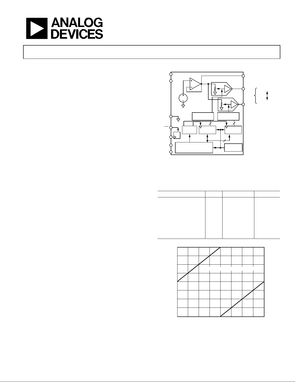
FUNCTIONAL BLOCK DIAGRAM
V
TP
V
AGND
CS
CLK
SDI
DGND
DD
V
2V
REF
DECODER SW
DRIVER A
12
A0
16-BIT
DAC A
REGISTER
ADDR
DECODE
EN
D15...D0
AD5399
X2×2
DECODER SW
DRIVER B
DAC B
REGISTER
12
POWER-ON
RESET
Figure 1.
V
= ((D – 2048)/4096 × 4 V) + 2 V for 0 ≤ D ≤ 4095, where D
OUT
is the decimal code.
Table 1. Examples of Twos Complement Codes
Twos Complement D Scale V
2047 4095 +FS 4.000
2046 4094 +FS – 1 LSB 3.999
1 2049 BZS + 1 LSB 2.001
0 2048 BZS 2.000
4095 2047 BZS – 1 LSB 1.999
2049 1 –FS + 1 LSB 0.001
2048 0 –FS 0.000
FS = Full Scale, BZS = Bipolar Zero Scale.
4.0
3.5
(V)
V
OUT
3.0
2.5
2.0
1.5
V
= [(0 – 2048)/4096 × 4V] + 2V
OUT
VBZ(V
) = 2V
REF
VBZ + 2V = 4V
V
OUTA
V
– 2V = 0V
V
OUTB
BZ
OUT
(V)
03469-B-001
×2
12
The AD5399 is available in the compact 1.1 mm low profile
MSOP-10 package. All parts are guaranteed to operate over the
extended industrial temperature range of –40°C to +105°C.
Rev. D
Information furnished by Analog Devices is believed to be accurate and reliable.
However, no responsibility is assumed by Analog Devices for its use, nor for any
infringements of patents or other rights of third parties that may result from its use.
Specifications subject to change without notice. No license is granted by implication
or otherwise under any patent or patent rights of Analog Devices. Trademarks and
registered trademarks are the property of their respective owners.
1.0
0.5
0
0 512 1024 1536 2048 2560 3072 3584 4096
TWOS COMPLEMENT CODE
Figure 2. Output vs. Twos Complement Code
One Technology Way, P.O. Box 9106, Norwood, MA 02062-9106, U.S.A.
Tel: 781.329.4700
Fax: 781.326.8703 © 2004 Analog Devices, Inc. All rights reserved.
www.analog.com
03469-B-002

AD5399
TABLE OF CONTENTS
Specifications..................................................................................... 3
Electrical Characteristics ............................................................. 3
Absolute Maximum Ratings............................................................ 4
ESD Caution.................................................................................. 4
Pin Configuration and Function Descriptions............................. 5
Timing Characteristics..................................................................... 6
REVISION HISTORY
6/04—Data sheet changed from Rev. C to Rev. D
Correction to Table 7 Caption ...................................................... 11
3/04—Data sheet changed from Rev. B to Rev. C
Changes to Specifications................................................................ 3
Changes to Table 4............................................................................ 5
Replaced Figures 4 and 5 ................................................................. 6
Changes to Operation Section ...................................................... 10
Changes to Table 6.......................................................................... 10
Typical Performance Characteristics..............................................7
Operation......................................................................................... 10
Power-Up/Power-Down Sequence .......................................... 10
Outline Dimensions....................................................................... 12
Ordering Guide .......................................................................... 12
11/03—Data sheet changed from Rev. A to Rev. B
Changes to Table 5 notes ................................................................. 5
Changes to Figures 8 and 9.............................................................. 7
Changes to Figure 12........................................................................ 8
Added Power-Up/Power-Down section...................................... 10
3/03—Data sheet changed from Rev. 0 to Rev. A
Change to Table 1 ............................................................................. 1
2/03—Revision 0: Initial Version
Rev. D | Page 2 of 12

AD5399
SPECIFICATIONS
ELECTRICAL CHARACTERISTICS
VDD = 5 V ± 10%, –40°C < TA < +105°C, unless otherwise noted.
Table 2.
Parameter Symbol Conditions Min Typ1 Max Unit
DC CHARACTERISTICS
Resolution N 12 Bits
Differential Nonlinearity Error DNL –1 ±0.5 +1 LSB
Codes 2048 to 2052, due to int. op amp offset –1.2 ±0.5 +1.2 LSB
Integral Nonlinearity Error INL –0.4 ±0.02 +0.4 %FS
Positive Full-Scale Error V
Bipolar Zero-Scale Error V
Negative Full-Scale Error V
ANALOG OUTPUTS
Nominal Positive Full-Scale V
Positive Full-Scale Tempco2 TCV
Code = 0xFF, TA = –40°C to +105°C –60 ±10 +60 ppm/°C
Nominal VBZ Output Voltage VBZ 1.995 2.000 2.004 V
Bipolar Zero Output Resistance2
VBZ Output Voltage Tempco TCVBZ T
T
Nominal Peak-to-Peak Output Swing |V
DIGITAL INPUTS
Input Logic High VIH V
Input Logic Low VIL V
Input Current IIL V
Input Capacitance2
POWER SUPPLIES
Power Supply Range V
Supply Current IDD V
Supply Current in Shutdown I
V
Power Dissipation3 P
Power Supply Sensitivity PSS ∆VDD = 5 V ± 10% –0.006 +0.003 +0.006 %/%
DYNAMIC CHARACTERISTICS2
Settling Time tS 0.1% error band 0.8 µs
Digital Feedthrough Q 10 nV-s
Bipolar Zero-Scale Glitch G 10 nV-s
Capacitive Load Driving Capability CL No oscillation 1000 pF
INTERFACE TIMING CHARACTERISTICS
2, 4
SCLK Cycle Frequency t
SCLK Clock Cycle Time t1 30 ns
Input Clock Pulse Width t2, t3 Clock level low or high 15 ns
Data Setup Time t4 5 ns
Data Hold Time t5 0 ns
CS
to SCLK Active Edge Setup Time
SCLK to CS Hold Time
Repeat Programming, CS High Time
1
Typical values represent average readings at 25°C and VDD = 5 V.
2
Guaranteed by design and not subject to production test.
3
P
is calculated from (IDD × VDD). CMOS logic level inputs result in minimum power dissipation.
DISS
4
See timing diagram (Figure 5) for location of measured values. All input control voltages are specified with tR = tF = 2 ns (10% to 90% of 3 V) and timed from a voltage
level of 1.5 V. Switching characteristics are measured using V
Code = 0xF –0.75 –0.15 +0.75 %FS
+FSE
Code = 0x000 –0.75 –0.15 +0.75 %FS
BZSE
Code = 0x800 –0.75 –0.15 +0.75 %FS
–FSE
Code = 0x7FF 4 V
OUTA/B
Code = 0x7FF, TA = 0°C to 70°C –40 ±10 +40 ppm/°C
OUTA/B
R
BZ
| + |V
+FS
C
5 pF
IL
DD RANGE
DD_SHDN
V
DISS
1 Ω
= 0°C to 70°C –40 ±10 +40 ppm/°C
A
= –40°C to +105°C –60 ±10 +60 ppm/°C
A
| Code 0x7FF to Code 0x800 4 V
–FS
= 5 V 2.4 V
DD
= 5 V 0.8 V
DD
= 0 V or 5 V, VDD = 5 V ±1 µA
IN
4.5 5.5 V
= VDD or VIL = 0 V 1.8 2.6 mA
IH
V
= VDD or VIL = 0 V, B14 = 0, TA = 0°C to 105°C 10 100 µA
IH
= VDD or VIL = 0 V, B14 = 0, TA = –40°C to 0°C 100 500 µA
IH
= VDD or VIL = 0 V, VDD = 5.5 V 9 13 mW
IH
33 MHz
CYC
5 ns
t
6
0 ns
t
7
30 ns
t
8
= 5 V. Input logic should have a 1 V/µs minimum slew rate.
DD
Rev. D | Page 3 of 12
AD5399
ABSOLUTE MAXIMUM RATINGS
TA = 25°C, unless otherwise noted.
Table 3.
Parameter Rating
VDD to GND –0.3 V, +7.5 V
V
, V
OUTA
Digital Input Voltages to GND 0 V, VDD + 0.3 V
Operating Temperature Range –40°C to +105°C
Maximum Junction Temperature (TJ
Storage Temperature –65°C to +150°C
Lead Temperature (Soldering, 10 sec) 300°C
Package Power Dissipation (T
Thermal Resistance, θJA, MSOP-10 206°C/W
, VBZ to GND 0 V, VDD
OUTB
) 150°C
MAX
J MAX
– TA)/θJA
ESD CAUTION
ESD (electrostatic discharge) sensitive device. Electrostatic charges as high as 4000 V readily accumulate on
the human body and test equipment and can discharge without detection. Although this product features
proprietary ESD protection circuitry, permanent damage may occur on devices subjected to high energy
electrostatic discharges. Therefore, proper ESD precautions are recommended to avoid performance
degradation or loss of functionality.
Stresses above those listed under Absolute Maximum Ratings
may cause permanent damage to the device. This is a stress
rating only; functional operation of the device at these or any
other conditions above those indicated in the operational
section of this specification is not implied. Exposure to absolute
maximum rating conditions for extended periods may affect
device reliability.
Rev. D | Page 4 of 12

AD5399
PIN CONFIGURATION AND FUNCTION DESCRIPTIONS
CLK
DGND
V
OUTB
V
OUTA
SDI
1
2
AD5399
3
TOP VIEW
(Not to Scale)
4
5
10
9
8
7
6
CS
V
TP
V
DD
AGND
V
BZ
03469-B-003
Figure 3. MSOP-10 Pin Configuration
Table 4. Pin Function Descriptions
Pin No. Mnemonic Description
1 CLK Serial Clock Input. Positive edge triggered.
2 SDI Serial Data Input. MSB first format.
3 DGND Digital Ground.
4 V
5 V
DAC B Voltage Output (A0 = Logic 1).
OUTB
DAC A Voltage Output (A0 = Logic 0).
OUTA
6 VBZ 2 V, Virtual Bipolar Zero (Active Output).
7 AGND Analog Ground.
8 VDD Positive Power Supply. Specified for operation at 5 V.
9 VTP Connect to VDD. Reserved for factory testing.
10
CS Chip Select (Frame Sync Input). Allows clock and data to shift into the shift register when CS goes from high to low.
th
After the 16
clock pulse, it is not necessary to bring CS high to shift the data to the output. However, CS should be
brought high any time after the 16th clock positive edge in order to allow the next programming cycle.
Table 5. Serial Data-Word Format
ADDR DATA
B15 B14 B13 B12 B11 B10 … B3 B2 B1 B0
A0 X SD 0 D11 D10 … D3 D2 D1 D0
MSB LSB
A0 Address Bit. Logic low selects DAC A and logic high selects DAC B.
Both channels are shut down when the SD bit is high. However, the A0 bit must be at the same state for shutdown
activation and deactivation. See the Shutdown Function section.
X Don’t Care.
SD Shutdown Bit. Logic high puts both DAC outputs and VBZ into high impedance. A0 bit must be at the same state for
shutdown activation and deactivation.
0 B12 must be 0.
D0–D11 Data Bits.
Rev. D | Page 5 of 12

AD5399
TIMING CHARACTERISTICS
1
SDI
0
1
SCLK
0
1
CS
0
A0 X SD 0 D11 D10 D9 D8 D7 D6 D5 D4 D3 D2 D1 D0
1
SDI
SCLK
V
OUT
0
1
0
1
CS
0
1
0
Dx Dx
t
6
Figure 4. Timing Diagram
Dx Dx
t
t
2
t
3
t
1
t
4
5
Figure 5. Detailed Timing Diagram
03469-C-001
t
7
t
8
t
S
±1LSB
ERROR
BAND
03469-C-002
Rev. D | Page 6 of 12

AD5399
TYPICAL PERFORMANCE CHARACTERISTICS
10
8
6
4
2
0
INL (LSB)
–2
–4
–6
–8
–10
0 512 1024 1536 2048 2560 3072 3584 4096
DAC B
DAC A
CODE (Decimal)
Figure 6. Integral Nonlinearity Errors
1.00
VDD = 5V
T
= 25°C
A
0.75
0.50
0.25
DAC A, B
VDD = 5V
= 25°C
T
A
03469-B-006
2.3
VDD = 5V
2.2
2.1
2.0
SUPPLY CURRENT (mA)
1.9
1.8
–60 –40 –20 0 20 40 60 80 100 120
TEMPERATURE (°C)
Figure 9. Supply Current vs. Temperature
2.4
VDD = 5V
= 25°C
T
A
2.3
(mA)
2.2
DD
03469-B-009
0
DNL (LSB)
–0.25
–0.50
–0.75
–1.00
0 512 1024 1536 2048 2560 3072 3584 4096
CODE (Decimal)
Figure 7. Differential Nonlinearity Errors
1.96
TA = 25°C
1.92
1.88
1.84
SUPPLY CURRENT (mA)
1.80
1.76
23 546
SUPPLY VOLTAGE (V)
Figure 8. Supply Current vs. Supply Voltage
03469-B-007
7
03469-B-008
2.1
2.0
SUPPLY CURRENT, I
1.9
1.8
234567
DIGITAL INPUT VOLTAGE, V
(V)
IH
Figure 10. Supply Current vs. Digital Input Voltage
4.5
VDD = 5V
T
= 25°C
A
4.0
3.5
3.0
2.5
2.0
1.5
SUPPLY CURRENT (mA)
1.0
0.5
0
10k 100k 1M 10M 100M
CLOCK FREQUENCY (Hz)
CODE = 0x555
CODE = 0x7FF
CODE = 0x000
Figure 11. Supply Current vs. Clock Frequency
03469-B-010
03469-B-011
Rev. D | Page 7 of 12

AD5399
1000
A)
100
µ
10
1
SHUTDOWN CURRENT (
VDD = 5V
NUMBER OF DEVICES
70
SS = 345
25°C to 85°C
60
50
40
30
20
10
0.1
–60 –40 –20 0 20 40 60 80 100 120 140
SHUTDOWN TEMPERATURE (°C)
Figure 12. Shutdown Current vs. Temperature
20
VDD = 5V
= 25°C
T
A
18
16
14
12
CURRENT SOURCING
CODE = 0x000 = 2V
10
8
6
LOAD CURRENT (mA)
4
2
0
–6–4–20246810
CURRENT SINKING
CODE = 0x000 = 2V
∆V
(mV)
OUT
CURRENT SINKING
CODE = 0x800 = 0V
Figure 13. Load Current vs. Voltage Drop
0.5
VDD = 5V
BURN-IN TEMPERATURE = 125°C
0.4
0.3
0.2
0.1
(mV)
0
OUT
∆V
–0.1
–0.2
–0.3
–0.4
–0.5
0 200 400 600 800 1000 1200
V
+FS
V
BZS
HOURS OF OPERATION
V
V
Figure 14. Long-Term Drift
–FS
BZ
0
03469-B-012
–45–40–35–30–25–20–15–10 –5 20 400 5 10 15 25 30 35
Figure 15. V
BZ
TEMPCO (ppm/°C)
Temperature Coefficient (TA = 25°C to 85°C)
03469-B-015
100
SS = 345
25°C to 105°C
80
60
40
NUMBER OF DEVICES
20
0
03469-B-013
–15 –10 –5 0 5 10 15 20 25 30 35 40 45 50
Figure 16. V
BZ
TEMPCO (ppm/°C)
Temperature Coefficient (TA = 25°C to 105°C)
03469-B-016
40
SS = 345
–40°C to +25°C
35
30
25
20
15
NUMBER OF DEVICES
10
5
0
03469-B-014
–45–40–35–30–25–20–15–10 –5 0 5 10 15 20 25 30 35 40
Figure 17. V
Temperature Coefficient (TA = –40°C to +25°C)
BZ
TEMPCO (ppm/°C)
03469-B-017
Rev. D | Page 8 of 12

AD5399
V
: 0.5V/DIV
OUT
100
90
100
90
TRACE 2 (WITH RINGING):
TRACE 1: NO LOAD
CL = 2nF
RL = 1kΩ
V
: 1V/DIV
OUT
CLK: 5V/DIV
10
0%
Figure 18. Large Signal Settling (0.5 µs/DIV)
100
90
CS: 5V/DIV
V
: 50mV/DIV
10
0%
OUT
Figure 19. Midscale Glitch and Digital Feedthrough (2 µs/DIV)
CLK: 5V/DIV
10
0%
03469-B-018
03469-B-020
Figure 20. Capacitive Load Output Performance (2 µs/DIV )
03469-B-019
Rev. D | Page 9 of 12

AD5399
OPERATION
The AD5399 provides a 12-bit, twos complement, dual voltage
output, digital-to-analog converter (DAC). It has an internal
reference with 2 V bipolar zero dc offset, where 0 ≤ V
The output transfer equation is
= ((D – 2048)/4096 × 4 V) + 2 V
V
OUT
where:
D is the 12-bit decimal code and not the twos complement code.
is with respect to ground.
V
OUT
In data programming, the data is loaded MSB first on the
positive clock edge (SCLK) after chip select (
) goes from high
CS
to low. The digital word is 16 bits wide, with the MSB, B15, as an
address bit (DAC A: A0 = 0; DAC B: A0 = 1). B14 is don’t care,
B13 is a shutdown bit, B12 must be logic low, and the last 12 bits
are data bits. An internal counter allows data transferred from
th
the shift register to the output after the 16
while
not necessary to bring
However,
stays low (see Figure 5). After the 16th clock pulse, it is
CS
high to shift the data to the output.
CS
should be brought high anytime after the 16th clock
CS
positive clock edge
positive edge in order to allow the next programming cycle.
Table 6. Input Logic Control Truth Table
CLK
Register Activity
CS
L H No Shift Register Effect
H H No Shift Register Effect
P L Shift One SDI Bit into the SR
16th P L
Transfer SR Data into DAC Register and Update
the Output
P = Positive Edge, X = Don't Care, SR = Shift Register.
The data setup and data hold times in the Specifications table
determine the timing requirements. The internal power-on reset
circuit clears the serial input registers to all 0s, and sets the two
DAC registers to a V
(zero code) of 2 V.
BZ
Software shutdown B13 turns off the internal REF and
amplifiers. The output is close to zero potential, and the digital
circuitry remains active such that new data can be written.
Therefore, the DAC register is refreshed with the new data once
the shutdown bit is deactivated.
All digital inputs are ESD protected with a series input resistor
and parallel Zener, as shown in Figure 21, that apply to digital
input pins CLK, SDA, and
. The basic connection is shown in
CS
Figure 22.
OUT
≤ 4 V.
1kΩ
LOGIC
03469-B-021
Figure 21. Equivalent ESD Protection Circuit
5V
C1
C2
10µF
0.1µF
V
DD
V
TP
AD5399
CS
CLK
SDI
Figure 22. Basic Connection
VBZ(V
AGNDDGND
REF
V
OUTA
)
(D–2048)/4096 × 4V + 2V
2V
03469-B-022
POWER-UP/POWER-DOWN SEQUENCE
Like most CMOS devices, it is recommended to power VDD and
ground prior to any digital signals. The ideal power-up
sequence is GND, V
applies to the power-down condition.
Layout and Power Supply Bypassing
It is a good practice to employ compact, minimum lead-length
layout design. The input leads should be as direct as possible
with a minimum conductor length. Ground paths should have
low resistance and low inductance.
Similarly, it is also good practice to bypass the power supplies
with quality capacitors for optimum stability. Supply leads to the
device should be bypassed with 0.01 µF to 0.1 µF disc or chip
ceramic capacitors. Low ESR 1 µF to 10 µF tantalum or electrolytic capacitors should also be applied at V
transient disturbance and to filter any low frequency ripple (see
Figure 23). Users should not apply switching regulators for V
due to the power supply rejection ratio degradation over
frequency.
V
DD
Figure 23. Power Supply Bypassing and Grounding Connection
Grounding
The DGND and AGND pins of the AD5399 refer to the digital
and analog ground references. To minimize the digital ground
bounce, the DGND terminal should be joined remotely at a
single point to the analog ground plane, as shown in Figure 23.
, and digital signals. The reverse sequence
DD
to minimize any
DD
AD5399
V
+
C2
10µF
C1
0.1µF
DD
AGND
DGND
03469-B-023
DD
Rev. D | Page 10 of 12

AD5399
Shutdown Function
The AD5399 shutdown function allows both DACs to be
shutdown simultaneously. However, the A0 and SD bits work in
tandem, and the A0 logic state must be the same for shutdown
activation and deactivation (see Table 7).
Table 7. Shutdown Activation and Deactivation Sequence.
Sequence
of Events
1
Data-Word
in Binary Shutdown Status
0X10 XXXX
Activate shutdown on both DACs.
XXXX XXXX
2
1X00 XXXX
Both DACs remain at shutdown.
XXXX XXXX
3
The A0 bit (MSB) must be in the same state when activating and deactivating
shutdown.
0X00 XXXX
XXXX XXXX
Deactivate shutdown. Both DACs
resume normal operation.
For users whose logic signals may be in three-state (random
levels) during power-up initialization, it is recommended to put
a pull-up resistor at the
pin to disable chip select (Figure 24).
CS
This avoids inadvertent shutdown as well as the inability to
deactivate shutdown due to an unknown A0 state. The resistor
value depends on the digital controller’s output impedance.
5V
C1
C2
10µF
0.1µF
Figure 24. Disable
R1
300kΩ
V
DD
V
TP
AD5399
CS
CLK
SDI
VBZ(V
REF
AGNDDGND
CS
for Random Logic Mode
V
OUTA
(D–2048)/4096 × 4V + V
)
2V
BZ
03469-B-022
Rev. D | Page 11 of 12

AD5399
OUTLINE DIMENSIONS
3.00 BSC
6
10
3.00 BSC
PIN 1
0.95
0.85
0.75
0.15
0.00
0.50 BSC
0.27
0.17
COPLANARITY
0.10
4.90 BSC
1
5
1.10 MAX
SEATING
PLANE
COMPLIANT TO JEDEC STANDARDS MO-187BA
0.23
0.08
Figure 25. 10-Lead Mini Small Outline Package [MSOP]
(RM-10)
Dimensions shown in millimeters
8°
0°
0.80
0.60
0.40
ORDERING GUIDE
Models Temperature Range Package Description Package Option Branding Ordering Quantity
AD5399YRM –40°C to +105°C MSOP RM-10 DSB 50
AD5399YRM-REEL7 –40°C to +105°C MSOP RM-10 DSB 1,000
© 2004 Analog Devices, Inc. All rights reserved. Trademarks and
registered trademarks are the property of their respective owners.
C03469–0–6/04(D)
Rev. D | Page 12 of 12
 Loading...