

Wideband Dual-Channel
FEATURES
2-quadrant multiplication/division
2 independent signal channels
Signal bandwidth of 60 MHz (I
Linear control channel bandwidth of 5 MHz
Low distortion (to 0.01%)
Fully calibrated, monolithic circuit
APPLICATIONS
Precise high bandwidth AGC and VCA systems
Voltage-controlled filters
Video signal processing
High speed analog division
Automatic signal-leveling
Square-law gain/loss control
GENERAL DESCRIPTION
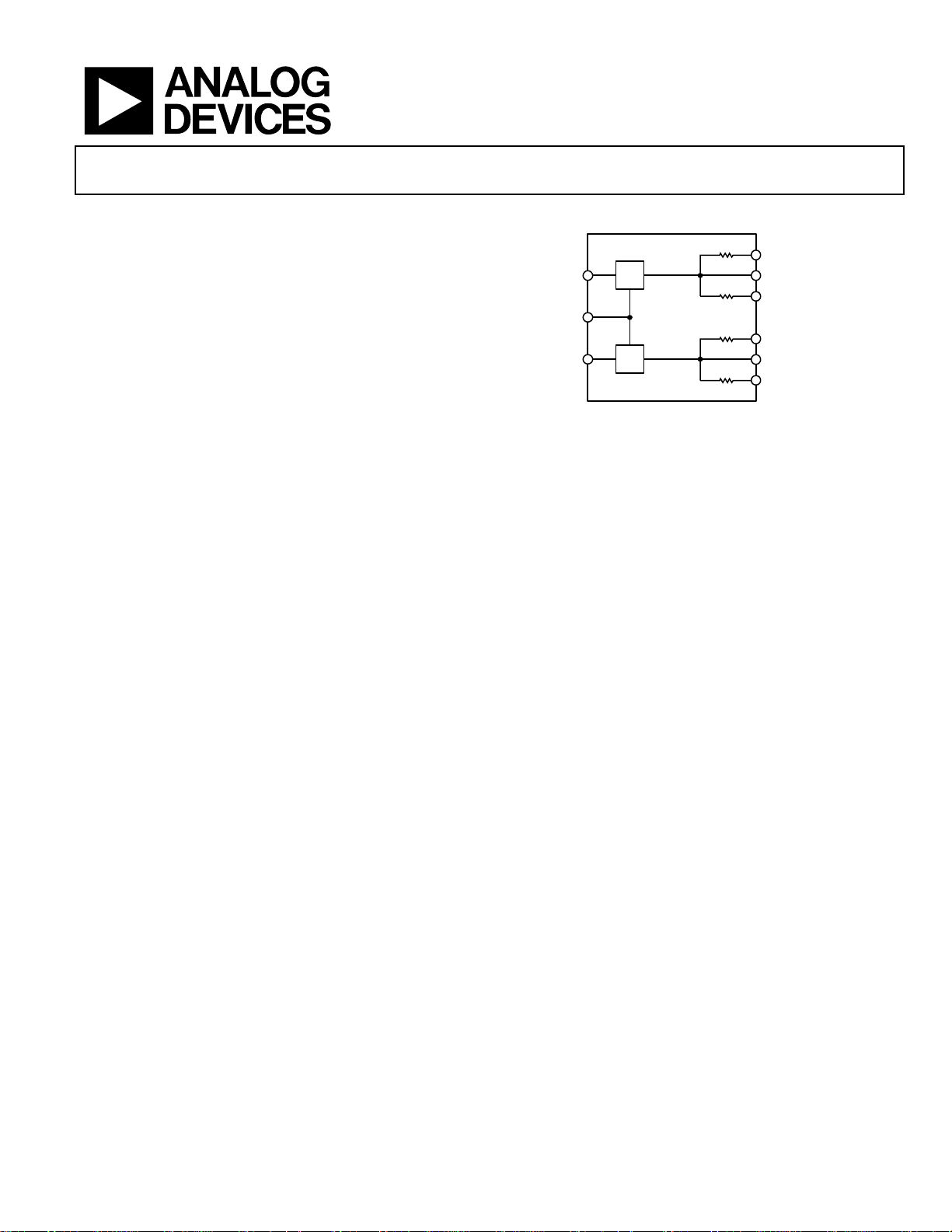
The AD539 is a low distortion analog multiplier having two
identical signal channels (Y1 and Y2), with a common X input
providing linear control of gain. Excellent ac characteristics up
to video frequencies and a −3 dB bandwidth of over 60 MHz are
provided. Although intended primarily for applications where
speed is important, the circuit exhibits good static accuracy in
computational applications. Scaling is accurately determined by
a band-gap voltage reference and all critical parameters are
laser-trimmed during manufacture.
The full bandwidth can be realized over most of the gain range
using the AD539 with simple resistive loads of up to 100 Ω.
Output voltage is restricted to a few hundred millivolts under
these conditions.
The two channels provide flexibility. In single-channel applications,
they can be used in parallel to double the output current, in
series to achieve a square-law gain function with a control range of
over 100 dB, or differentially to reduce distortion. Alternatively,
OUT
)
Linear Multiplier/Divider
AD539
FUNCTIONAL BLOCK DIAGRAM
AD539
V
Y1
V
X
V
Y2
×
×
they can be used independently, as in audio stereo applications,
with low crosstalk between channels. Voltage-controlled filters
and oscillators using the state-variable approach are easily
designed, taking advantage of the dual channels and common
control. The AD539 can also be configured as a divider with
signal bandwidths up to 15 MHz.
Power consumption is only 135 mW using the recommended
±5 V supplies. The AD539 is available in three versions: the J
and K grades are specified for 0 to 70°C operation and S grade is
guaranteed over the extended range of −55°C to +125°C. The J and
K grades are available in either a hermetic ceramic SBDIP (D-16)
or a low cost PDIP (N-16), whereas the S grade is available in
ceramic SBDIP (D-16) or LCC (E-20-1). The S grade is available in MIL-STD-883 and Standard Military Drawing (DESC)
Number 5962-8980901EA versions.
6kΩ
6kΩ
6kΩ
6kΩ
Figure 1.
W1
CHAN1 OUTPUT
Z1
Z2
CHAN2 OUTPUT
W2
09679-001
Rev. B
Information furnished by Analog Devices is believed to be accurate and reliable. However, no
responsibility is assumed by Anal og Devices for its use, nor for any infringements of patents or ot her
rights of third parties that may result from its use. Specifications subject to change without notice. No
license is granted by implication or otherwise under any patent or patent rights of Analog Devices.
Trademarks and registered trademarks are the property of their respective owners.
One Technology Way, P.O. Box 9106, Norwood, MA 02062-9106, U.S.A.
Tel: 781.329.4700 www.analog.com
Fax: 781.461.3113 ©1983–2011 Analog Devices, Inc. All rights reserved.

AD539
TABLE OF CONTENTS
Features.............................................................................................. 1
Applications....................................................................................... 1
Functional Block Diagram .............................................................. 1
General Description ......................................................................... 1
Revision History ............................................................................... 2
Specifications..................................................................................... 3
Pin Configurations and Function Descriptions ........................... 5
Typical Performance Characteristics ............................................. 7
Theory of Operation ...................................................................... 10
Circuit Description..................................................................... 10
General Recommendations....................................................... 10
REVISION HISTORY
4/11—Rev. A to Rev. B
Updated Format..................................................................Universal
Changed Pin Configuration to Functional Block Diagram........ 1
Changes to General Description Section ...................................... 1
Added Pin Configurations and Function Descriptions
Section................................................................................................ 5
Added Table 2; Renumbered Sequentially .................................... 5
Added Table 3.................................................................................... 6
Added Typical Performance Characteristics Section .................. 7
Added Figure 6 and Figure 9; Renumbered Sequentially ........... 7
Changes to Figure 18...................................................................... 10
Transfer Function....................................................................... 11
Dual Signal Channels................................................................. 11
Common Control Channel....................................................... 11
Flexible Scaling ........................................................................... 11
Applications Information.............................................................. 12
Basic Multiplier Connections................................................... 12
A 50 MHz Voltage-Controlled Amplifier ............................... 15
Basic Divider Connections ....................................................... 16
Outline Dimensions....................................................................... 17
Ordering Guide .......................................................................... 18
Moved Dual Signal Channels Section, Common Control
Channel Section, and Flexible Scaling Section........................... 11
Changes to Figure 20...................................................................... 12
Changes to Table 4, Figure 21, and Table 5................................. 13
Changes to Figure 22 and Figure 23............................................. 14
Changes to Figure 24...................................................................... 15
Changes to Figure 25...................................................................... 16
Updated Outline Dimensions....................................................... 17
Changes to Ordering Guide.......................................................... 18
12/91—Rev. 0 to Rev. A
Rev. B | Page 2 of 20
AD539
SPECIFICATIONS
TA = 25°C, VS = ±5 V, unless otherwise specified. VY = VY1 − VY2, VX = VX1 – VX2. All minimum and maximum specifications are
guaranteed.
Table 1.
AD539J AD539K AD539S
Parameter Test Conditions/Comments Min Typ Max Min Typ Max Min Typ Max Unit
SIGNAL CHANNEL DYNAMICS
Minimal Configuration
See Figure 22
Bandwidth, −3 dB RL = 50 Ω, CC = 0.01 μF 30 60 30 60 30 60 MHz
Maximum Output 0.1 V < VX < 3 V, VY ac = 1 V rms −10 −10 −10 dBm
Feedthrough VX = 0 V, VY ac = 1.5 V rms
f < 1 MHz −75 −75 −75 dBm
f = 20 MHz −55 −55 −55 dBm
Differential Phase Linearity
−1 V < VY dc < +1 V f = 3.58 MHz, VX = 3 V,
ac = 100 mV
V
Y
−2 V < VY dc < +2 V f = 3.58 MHz, VX = 3 V,
ac = 100 mV
V
Y
Group Delay VX = 3 V, VY ac = 1 V rms,
±0.2 ±0.2 ±0.2 Degrees
±0.5 ±0.5 ±0.5 Degrees
4 4 4 ns
f = 1 MHz
Standard 2-Channel Multiplier
See Figure 20
Maximum Output VX = 3 V, VY ac = 1.5 V rms 4.5 4.5 4.5 V
Feedthrough, f < 100 kHz VX = 0 V, VY ac = 1.5 V rms 1 1 1 mV rms
Crosstalk (Channel 1 to
Channel 2)
VY1 = 1 V rms, VY2 = 0 V,
= 3 V, f < 100 kHz
V
X
−40 −40 −40 dB
RTO Noise, 10 Hz to 1 MHz VX = 1.5 V, VY = 0 V 200 200 200 nV/√Hz
THD + Noise
VX = 1 V f = 10 kHz, VY ac = 1 V rms 0.02 0.02 0.02 %
VY = 3 V f = 10 kHz, VY ac = 1 V rms 0.04 0.04 0.04 %
Wideband 2-Channel Multiplier
See Figure 20
Bandwidth, −3 dB (LH0032) 0.1 V < VX < 3 V,
V
ac = 1 V rms
Y
25 25 25 MHz
Maximum Output VX = 3 V VY ac = 1.5 V rms, f = 3 MHz 4.5 4.5 4.5 V rms
Feedthrough VX = 0 V VY ac = 1.0 V rms, f = 3 MHz 14 14 14 mV rms
Wideband Single-Channel VCA
See Figure 24
Bandwidth, −3 dB 0.1 V < VX < 3 V,
V ac = 1 V rms
Y
50 50 50 MHz
Maximum Output 75 Ω load ±1 ±1 ±1 V
Feedthrough VX = −0.01 V, f = 5 MHz −54 −54 −54 dB
CONTROL CHANNEL DYNAMICS
Bandwidth, −3 dB CC = 3000 pF, VX dc = 1.5 V,
V
ac = 100 mV rms
X
SIGNAL INPUTS, V AND V
Y1 Y2
5 5 5 MHz
Nominal Full-Scale Input ±2 ±2 ±2 V
Operational Range, Degraded
−VS ≤ 7 V ±4.21
±4.2
Performance
Input Resistance 400 400 400 kΩ
Bias Current 10 301 10 201 10 301 μA
Offset Voltage VX = 3 V, VY = 0 V 5 201 5 101 5 201 mV
T to T
MIN MAX
10 5 15 35 mV
Power Supply Sensitivity VX = 3 V, VY = 0 V 2 2 2 mV/V
1
V
±4.21
Rev. B | Page 3 of 20

AD539
AD539J AD539K AD539S
Parameter Test Conditions/Comments Min Typ Max Min Typ Max Min Typ Max Unit
CONTROL INPUT, VX
Nominal Full-Scale Input 3.0 3.0 3.0 V
Operational Range, Degraded
Performance
Input Resistance2 500 500 500 Ω
Offset Voltage 1 41 1 21 1 41 mV
T
to T
MIN
3 2 2 51 mV
MAX
Power Supply Sensitivity 30 30 30 μV/V
Gain
Absolute Gain Error VX = 0.1 V to 3.0 V, VY = ±2 V 0.2 0.41 0.1
T
to T
MIN
V
MAX
CURRENT OUTPUT2
Full-Scale Output Current VX = 3 V, VY = ±2 V ±1 ±1 ±1 mA
Peak Output Current VX = 3.3 V, VY = ±5 V,
Output Offset Current VX = 0 V, VY = 0 V 0.2 1.51 0.2 1.51 0.2 1.51 μA
Output Offset Voltage3
Output Resistance 1.2 1.2 1.2 kΩ
Scaling Resistors
Channel 1 Z1, W1 to CH1 6 6 6 kΩ
Channel 2 Z2, W2 to CH2 6 6 6 kΩ
VOLTAGE OUTPUTS, VW1 AND V
Multiplier Transfer Function
Either Channel VW = −VX × VY/VU V
Multiplier Scaling Voltage, VU 0.981 1.0 1.021 0.991 1.0 1.011 0.981 1.0 1.021 V
Accuracy 0.5 21 0.5 11 0.5 2 %
T
to T
MIN
1 0.5 1.0 31 %
MAX
Power Supply Sensitivity 0.04 0.04 0.04 %/V
Total Multiplication Error4 V
T
to T
MIN
2 1 2 41 %
MAX
Control Feedthrough VX = 0 V to 3 V, VY = 0 V 25
T
to T
MIN
30 15 60 1201 mV
MAX
TEMPERATURE RANGE
Rated Performance 0 +70 0 +70 −55 +125 °C
POWER SUPPLIES
Operational Range ±4.5 ±15 ±4.5 ±15 ±4.5 ±15 V
Current Consumption
+VS 8.5 10.21 8.5 10.21 8.5 10.21 mA
−VS 18.5 22.21 18.5 22.21 18.5 22.21 mA
1
Tested on all production units at final electrical test. Results from those tests are used to calculate outgoing quality levels.
2
Resistance value and absolute current outputs subject to 20% tolerance.
3
Specification assumes the external op amp is trimmed for negligible input offset.
4
Includes all errors.
+3.2 +3.2 +3.2 V
See Figure 20
= 0.1 V to 3.0 V, VY = ±2 V 0.3 0.15 0.25 0.51 dB
X
1
0.2 0.4
0.2
±2 ±2.8 ±2 ±2.8 ±2 ±2.8 mA
= ±7.5 V
V
S
See Figure 20, VX = 0 V,
V
= 0 V
Y
3
See Figure 20
W2
≤ 3 V, −2 V < VY < +2 V 1 2.5 0.6 1.5 1 2.5 % FSR
X
3 10
1
3 101 3 101 mV
60
1
= −VX × VY/VU V
W
15 30
1
15 601 mV
= −VX × VY/VU
W
1
dB
Rev. B | Page 4 of 20
AD539
P
PIN CONFIGURATIONS AND FUNCTION DESCRIPTIONS
X
V
HF COM
3
V
4
Y1
+V
5
S
6
NC
–V
S
V
Y2
7
8
TOP VIEW
(Not to Scale)
AD539
19Z120W11NC2
18
CHAN1 OUTPUT
17
BASE COMM ON
16
NC
15
BASE COMM ON
14
CHAN2 OUTPUT
9
INPUT COMMON
13Z212W211NC10
NOTES
1. NC = NO CONNECT. DO NOT
CONNECT TO THIS PIN.
OUTPUT COMMON
09679-002
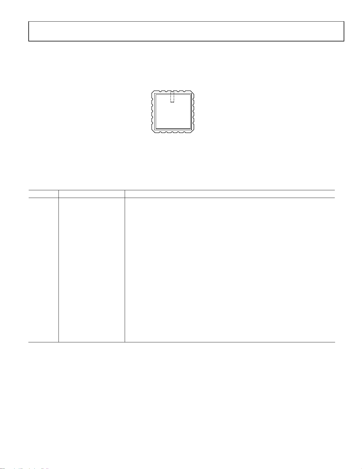
Figure 2. 20-Lead LLC Pin Configuration (E-20-1)
Table 2. 20-Lead LLC Pin Function Descriptions
Pin No. Mnemonic Description
1 NC No Connect. Do not connect to this pin.
2 VX Control Channel Input.
3 HF COMP High Frequency Compensation.
4 VY1 Channel 1 Input.
5 +VS Positive Supply Rail.
6 NC No Connect. Do not connect to this pin.
7 –VS Negative Supply Rail.
8 VY2 Channel 2 Input.
9 INPUT COMMON Internal Common Connection for the Input Amplifier Circuitry.
10 OUTPUT COMMON Internal Common Connection for the Output Amplifier Circuitry.
11 NC No Connect.
12 W2 6 kΩ Feedback Resistor for Channel 2.
13 Z2 6 kΩ Feedback Resistor for Channel 2.
14 CHAN2 OUTPUT Channel 2 Product of VX and VY2.
15 BASE COMMON Increases Negative Output Compliance.
16 NC No Connect. Do not connect to this pin.
17 BASE COMMON Increases Negative Output Compliance.
18 CHAN1 OUTPUT Channel 1 Product of VX and VY1.
19 Z1 6 kΩ Feedback Resistor for Channel 1.
20 W1 6 kΩ Feedback Resistor for Channel 1.
Rev. B | Page 5 of 20
AD539
V
1
X
HF COMP
INPUT COMMON
OUTPUT COMMON
V
+V
–V
V
Y1
S
S
Y2
2
3
AD539
4
TOP VIEW
(Not to Scale)
5
6
7
8
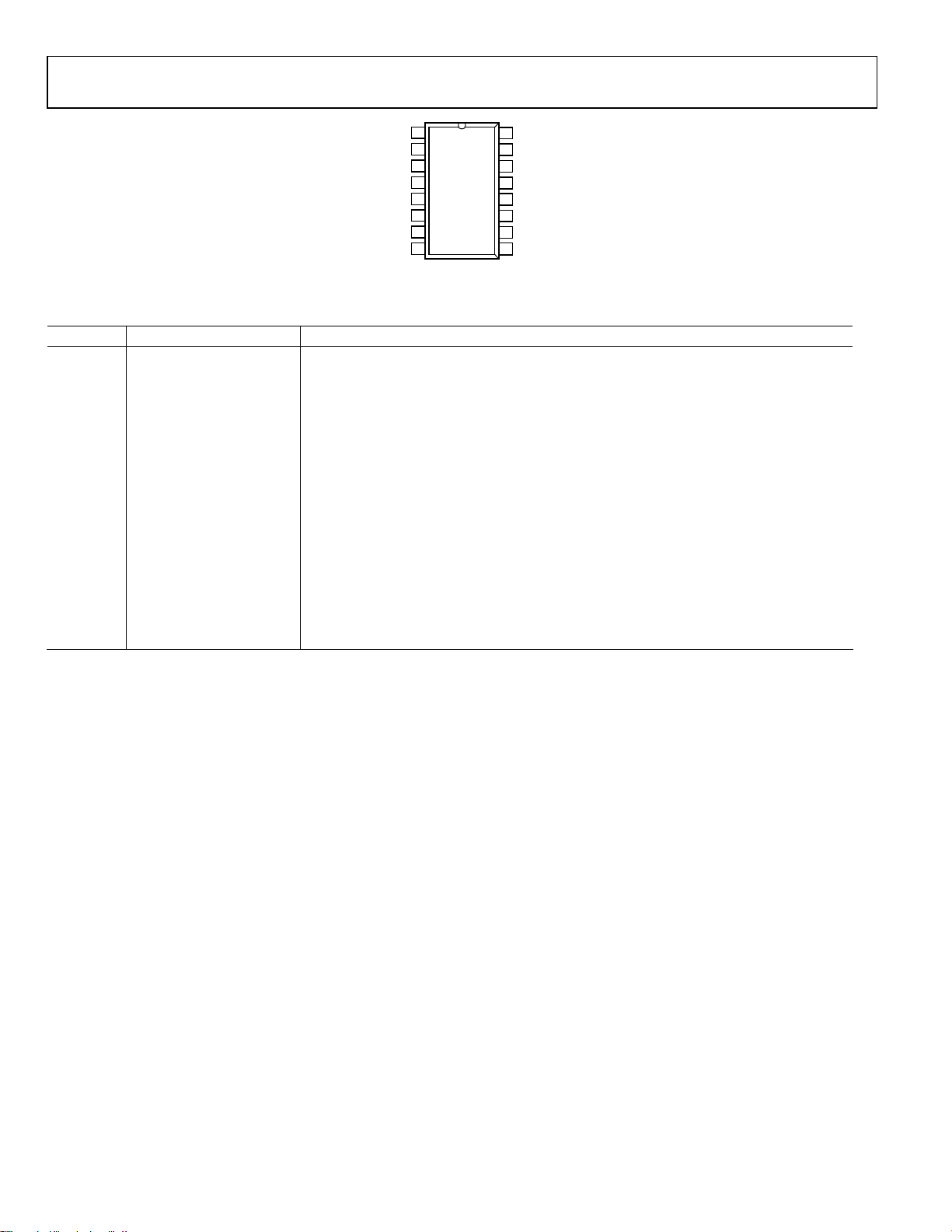
Figure 3. 16-Lead PDIP and SBDIP Pin Configurations (N-16, D-16)
Table 3. 16-Lead PDIP and SBDIP Pin Function Descriptions
Pin No. Mnemonic Description
1 VX Control Channel Input.
2 HF COMP High Frequency Compensation.
3 VY1 Channel 1 Input.
4 +VS Positive Supply Rail.
5 –VS Negative Supply Rail.
6 VY2 Channel 2 Input.
7 INPUT COMMON Internal Common Connection for the Input Amplifier Circuitry.
8 OUTPUT COMMON Internal Common Connection for The Output Amplifier Circuitry.
9 W2 6 kΩ Feedback Resistor for Channel 2.
10 Z2 6 kΩ Feedback Resistor for Channel 2.
11 CHAN2 OUTPUT Channel 2 Product of VX and VY2.
12 BASE COMMON Increases Negative Output Compliance.
13 BASE COMMON Increases Negative Output Compliance.
14 CHAN1 OUTPUT Channel 1 Product of VX and VY1.
15 Z1 6 kΩ Feedback Resistor for Channel 1.
16 W1 6 kΩ Feedback Resistor for Channel 1.
W1
16
15
Z1
14
CHAN1 OUTPUT
13
BASE COMMON
12
BASE COMMON
11
CHAN2 PUTPUT
10
Z2
9
W2
09679-003
Rev. B | Page 6 of 20

AD539
TYPICAL PERFORMANCE CHARACTERISTICS
VY = VY1 − VY2, VX = VX1 – VX2, unless otherwise noted.
3
2
)
X
AD539J, S
SPECS
1
AD539K
0
SPECS
–1
GAIN/LOSS ERRORS ( dB)
–2
–3
0.01 0.1 1 10
CONTROL VOLTAGE (V
Figure 4. Maximum AC Gain Error Boundaries
0.20
f = 10kHz
0.15
100
90
10
0%
09679-004
Figure 7. Multiplier Pulse Response Using LH0032 Op Amp, V
100
90
1V 50n s
2V
VX = +3V
1V 50n s
= 3 V
X
09679-007
0.10
V
= 1.5V rms
Y
0.05
V
= 0.5V rms
TOTAL HARMONIC DISTORTI ON (%)
0
01 2
CONTROL VOLTAGE (V)
Y
3
Figure 5. Total Harmonic Distortion vs. Control Voltage
20
10
0
–10
–20
–30
–40
HIGH FREQUENCY RESPONSE (dB)
–50
–60
100k 1M 10M 100M
VX = 3.162V
VX = 1.00V
VX = 0.316V
VX = 0.1V
VX = 0.032V
VX = 0.01V
FEEDTHROUGH
= –0.01V
V
X
FREQUENCY (Hz)
Figure 6. Multiplier High Frequency Response Using LH0032 Op Amps
10
0%
09679-005
100mV
VX = +0.1V
09679-008
Figure 8. Multiplier Pulse Response Using LH0032 Op Amp, VX = 0.1 V
0
–10
–20
–30
–40
–50
HIGH FREQUENCY RESPONSE (dB)
–60
–70
100k 1M 10M 100M
09679-006
VX = 3.162V
VX = 1.00V
VX = 0.316V
VX = 0.1V
VX = 0.032V
VX = 0.01V
FREQUENCY (Hz)
09679-009
Figure 9. High Frequency Response in Minimal Configuration
Rev. B | Page 7 of 20

AD539
2
100
1
0
90
20mV
100µs
–1
PHASE LI NEARITY (Degrees)
–2
05
FREQUENCY (MHz)
10
09679-010
Figure 10. Phase Linearity Error in Minimal Configuration
5.0
f = 3.579MHz
= 0.1V
V
2.5
0
–2.5
PHASE LINEARITY (Degrees)
–5.0
–2 –1 10
X
= 0.3V
V
X
V
= 1V
X
= 3V
V
X
SIGNAL INPUT BIAS VOLTAGE (V)
2
09679-011
Figure 11. Differential Phase Linearity in Minimal Configuration for a Typical
Device
20mV
100
90
10
0%
100µs
09679-012
Figure 12. Control Feedthrough One Channel of Figure 22
10
0%
Figure 13. Control Feedthrough Differential Mode of Figure 22
0.050
V
= 1.5V rms
Y
0.025
= 0.5V rms
V
Y
TOTAL HARMONIC DISTO RTION (%)
0
01 2
CONTROL VO LTAGE (V)
f = 10kHz
Figure 14. Distortion in Differential Mode Using LH0032 Op Amp
10
VX = +3.162V
0
VX = +1.00V
–10
VX = +0.316V
–20
VX = +0.1V
–30
VX = +0.032V
RESPONSE (dB)
–40
VX = +0.01V
–50
–60
Figure 15. AC Response of the VCA at Different Gains, V
VX = –0.01V
110
FREQUENCY ( MHz)
= 0.5 V RMS
Y
9679-013
3
09679-014
100
09679-015
Rev. B | Page 8 of 20

AD539
20ns2V 500µV
100
90
V
OUT
10
0%
V
IN
Figure 16. Transient Response of the Voltage-Controlled Amplifier,
= +2 V, VY = ±1 V
V
X
50
VX = +0.01V
40
VX = +0.032V
30
VX = +0.1V
20
VX = +0.316V
10
GAIN (dB)
VX = +1V
0
VX = +3.162V
–10
9679-016
–20
10k 100k 1M 10M
FREQUENCY (Hz)
Figure 17. High Frequency Response of Divider in Figure 25
09679-017
Rev. B | Page 9 of 20

AD539
V
THEORY OF OPERATION
CIRCUIT DESCRIPTION
Figure 18 shows a simplified schematic of the AD539. Q1 to Q6
are large-geometry transistors designed for low distortion and
low noise. Emitter-area scaling further reduces distortion: Q1 is
three times larger than Q2; Q4 and Q5 are each three times
larger than Q3 and Q6 and are twice as large as Q1 and Q2. A
stable reference current of I
band gap reference circuit and applied to the common emitter
node of a controlled cascode formed by Q1 and Q2. When V
0 V, all of I
flows in Q1 due to the action of the high gain
REF
control amplifier, which lowers the voltage on the base of Q2.
As V
is raised, the fraction of I
X
balance the control current, V
V
(3 V) this fraction is 0.873. Because the base of Q1, Q4, and
X
Q5 are at ground potential and the bases of Q2, Q3, and Q6 are
commoned, all three controlled cascodes divide the current
applied to their emitter nodes in the same proportion. The
control loop is stabilized by the external capacitor, C
The signal voltages, V
Y1
are first converted to currents by voltage-to-current converters
with a g
of 575 μmhos. Thus, the full-scale input of ±2 V
m
becomes a current of ±1.15 mA, which is superimposed on a
bias of 2.75 mA and applied to the common emitter node of
controlled cascode Q3/Q4 or Q5/Q6. As previously explained,
the proportion of this current steered to the output node is
linearly dependent on V
inputs, a signal of ±1 mA (0.873 × ±1.15 mA) and a bias
component of 2.4 mA (0.873 × 2.75 mA) appear at the output.
The bias component absorbed by the 1.25 kΩ resistors also
connected to V
and the resulting signal current can be applied
X
to an external load resistor (in which case scaling is not
accurate) or can be forced into either or both of the 6 kΩ
feedback resistors (to the Z and W nodes) by an external op
amp. In the latter case, scaling accuracy is guaranteed.
0V TO +3V FS
BASE COMMON
= 1.375 mA is produced by a
REF
X
flowing in Q2 is forced to
REF
/2.5 kΩ. At the full-scale value of
X
.
C
and VY2 (generically referred to as VY),
. Therefore, for full-scale VX and VY
X
X
1
1.2mA FS
13
I
REF
1.375mA
S
S
4
5
BAND-GAP
REFERENCE
GENERATOR
+V
–V
2.5kΩ 1.25kΩ
Q1 Q2 Q3 Q4 Q5 Q6
=
Figure 18. Simplified Schematic of AD539 Multiplier (16-Lead SBDIP and PDIP Shown)
CONTROL
AMPLIFIER
HF COMP
±2V FS
2
V
Y1
=
OUTPUT
CC (EXT)
3nF MIN
CHAN1
±1mA FS ±1mA FS
3
GENERAL RECOMMENDATIONS
The AD539 is a high speed circuit and requires considerable
care to achieve its full performance potential. A high quality
ground plane should be used with the device either soldered
directly into the board or mounted in a low profile socket. In
Figure 18, an open triangle denotes a direct, short connection
to this ground plane; the BASE COMMON pins (Pin 12 and
Pin 13) are especially prone to unwanted signal pickup. Power
supply decoupling capacitors of 0.1 μF to 1 μF should be
connected from the +V
ground plane. In applications using external high speed op
amps, use separate supply decoupling. It is good practice to
insert small (10 Ω) resistors between the primary supply and
the decoupling capacitor.
The control amplifier compensation capacitor, C
likewise have short leads to ground and a minimum value of
3 nF. Unless maximum control bandwidth is essential, it is
advisable to use a larger value of 0.01 μF to 0.1 μF to improve
the signal channel phase response, high frequency crosstalk,
and high frequency distortion. The control bandwidth is
inversely proportional to this capacitance, typically 2 MHz for C
0.01 μF, V
= 1.7 V. The bandwidth and pulse response of the
X
control channel can be improved by using a feedforward
capacitor of 5% to 20% the value of C
HF COMP pins (Pin 1 and Pin 2). Optimum transient response
results when the rise/fall time of V
control channel response time.
V
should not exceed the specified range of 0 V to 3 V. The ac
X
gain is zero for V
(see Figure 18) causing control feedthrough. Recovery time
from negative values of V
signal Schottky diode with its cathode connected to HF COMP
(Pin 2) and its anode grounded. This constrains the voltage
swing on C
. Above VX = 3.2 V, the ac gain limits at its
C
maximum value, but any overdrive appears as control
feedthrough at the output.
6kΩ
14
16
6kΩ
15
INPUT COMMON
W1
Z1
9
W2
10
Z2
12
7
and −VS pins (Pin 4 and Pin 5) to the
S
, should
C
between the VX and
C
are commensurate with the
X
< 0 V but there remains a feedforward path
X
can be improved by adding a small
X
1.25kΩ
6kΩ
6kΩ
CHAN2
11
OUTPUT
OUTPUT
8
COMMON
V
6
±2V FS
Y2
09679-018
=
C
Rev. B | Page 10 of 20

AD539
V
The power supplies to the AD539 can be as low as ±4.5 V and as
high as ±16.5 V. The maximum allowable range of the signal
inputs, V
value is 2.5 V above −V
, is approximately 0.5 V above +VS; the minimum
Y
. To accommodate the peak specified
S
inputs of ±4.2 V the supplies should be nominally +5 V and
−7.5 V. Although there is no performance advantage in raising
supplies above these values, it may often be convenient to use
the same supplies as for the op amps. The AD539 can tolerate
the excess voltage with only a slight effect on dc accuracy but
dissipation at ±16.5 V can be as high as 535 mW, and some
form of heat sink is essential in the interests of reliability.
TRANSFER FUNCTION
In using any analog multiplier or divider, careful attention must
be paid to the matter of scaling, particularly in computational
applications. To be dimensionally consistent, a scaling voltage
must appear in the transfer function, which, for each channel
of the AD539 in the standard multiplier configuration (see
Figure 20), is
V
= −VXVY/V
W
where the VX and VY inputs, the VW output, and the scaling
voltage, V
, are expressed in a consistent unit, usually volts.
U
In this case, V
acceptable in the interest of simplification to use the less rigorous
expression
= −VXV
V
W
where it is understood that all signals must be expressed in volts,
that is, they are rendered dimensionless by division by 1 V.
The accuracy specifications for V
two feedback resistors supplied with each channel, because
these are very closely matched, or they can be used in parallel to
halve the gain (double the effective scaling voltage), when
V
= −VXVY/2
W
When an external load resistor, R
longer exact because the internal thin film resistors, although
trimmed to high ratiometric accuracy, have an absolute
tolerance of 20%. However, the nominal transfer function is
V
= −VXVY/VU’
W
where the effective scaling voltage, V
each channel using the formula
V
’ = VU (5RL + 6.25)/RL
U
where R
100 Ω, V
is expressed in kilohms. For example, when RL =
L
’ = 67.5 V. Tabl e 5 provides more detailed data for the
U
case where both channels are used in parallel. The AD539 can
U
is fixed by the design to be 1 V and it is often
U
Y
allow the use of either of the
U
, is used, the scaling is no
L
’, c an be c a l c ul at ed fo r
U
also be used with no external load (CHAN2 OUTPUT, Pin 11,
or CHAN1 OUTPUT, Pin 14, open circuit), when VU’ is
precisely 5 V.
DUAL SIGNAL CHANNELS
The signal voltage inputs, VY1 and VY2, have nominal full-scale
(FS) values of ±2 V with a peak range to ±4.2 V (using a negative
supply of 7.5 V or greater). For video applications where
differential phase is critical, a reduced input range of ±1 V is
recommended, resulting in a phase variation of typically ±0.2°
at 3.579 MHz for full gain. The input impedance is typically
400 kΩ shunted by 3 pF. Signal channel distortion is typically
well under 0.1% at 10 kHz and can be reduced to 0.01% by using
the channels differentially.
COMMON CONTROL CHANNEL
The control channel accepts positive inputs, VX, from 0 V to 3 V
FS, ±3.3 V peak. The input resistance is 500 Ω. An external,
grounded capacitor determines the small-signal bandwidth and
recovery time of the control amplifier; the minimum value of
3 nF allows a bandwidth at midgain of about 5 MHz. Larger
compensation capacitors slow the control channel but improve
the high frequency performance of the signal channels.
FLEXIBLE SCALING
Using either one or two external op amps in conjunction with
the on-chip 6 kΩ scaling resistors (see Figure 19), the output
currents (nominally ±1 mA FS, ±2.25 mA peak) can be
converted to voltages with accurate transfer functions of V
−V
/2, VW = −VXVY, or VW = −2VXVY (where the VX and VY
XVY
inputs and V
output are expressed in volts), with correspond-
W
i n g f u l l - s ca le o u t pu ts of ± 3 V, ± 6 V, a n d ± 12 V. A lt e r na t i v el y,
low impedance grounded loads can be used to achieve the full
signal bandwidth of 60 MHz, in which mode the scaling is less
accurate.
Z1
CHAN1
MULTIPLY
Y1
V
Y2
V
X
CHAN2
MULTIPLY
Z2
Figure 19. Block Diagram Showing Scaling Resistors and External Op Amps
–
EXTRNAL
OP AMPS
–
W1
V
= –VXV
W1
VW2 = –VXV
W2
Y1
Y2
=
W
09679-019
Rev. B | Page 11 of 20

AD539
APPLICATIONS INFORMATION
BASIC MULTIPLIER CONNECTIONS
Figure 20 shows the connections for the standard dual-channel
multiplier, using op amps to provide useful output power and
the AD539 feedback resistors to achieve accurate scaling. The
transfer function for each channel is
V
= −VXVY
W
where the inputs and outputs are expressed in volts (see the
Transf e r Funct i on section).
At the nominal full-scale inputs of V
full-scale outputs are ±6 V. Depending on the choice of op amp,
their supply voltages may need to be about 2 V more than the
peak output. Thus, supplies of at least ±8 V are required; the
AD539 can share these supplies. Higher outputs are possible if
V
and VY are driven to their peak values of +3.2 V and ±4.2 V,
X
respectively, when the peak output is ±13.4 V. This requires
operating the op amps at supplies of ±15 V. Under these conditions, it is advisable to reduce the supplies to the AD539 to
±7.5 V to limit its power dissipation; however, with some form
of heat-sinking, it is permissible to operate the AD539 directly
from ±15 V supplies.
V
X
V
Y1
V
Y2
NOTES
1. ALL DEC OUPLING CAPACITO RS ARE 0.47µF CERAMIC.
1
CC = 3nF
V
HF COMP
2
3
V
+V
S
4
+V
–V
S
5 12
–V
V
6 11
INPUT
7 10
COMMON
OUTPUT
8 9
COMMON
X
Y1
Y2
S
S
AD539
Figure 20. Standard Dual-Channel Multiplier
(16-Lead SBDIP and PDIP Shown)
CHAN1
OUTPUT
BASE
COMMON
CHAN2
OUTPUT
W1
Z1
Z2
W2
Viewed as a voltage-controlled amplifier, the decibel gain is simply
G = 20 log V
where V
V
is expressed in volts. This results in a gain of 10 dB at
X
= 3.162 V, 0 dB at VX = 1 V, −20 dB at VX = 0.1 V, and so on.
X
X
In many ac applications, the output offset voltage (for V
= 0 V) is not a major concern; however, it can be elimi-
or V
Y
nated using the offset nulling method recommended for the
particular op amp, with V
At small values of V
= VY = 0 V.
X
, the offset voltage of the control channel
X
degrades the gain/loss accuracy. For example, a ±1 mV offset
uncertainty causes the nominal 40 dB attenuation at V
0.01 V to range from 39.2 dB to 40.9 dB. Figure 4 shows the
maximum gain error boundaries based on the guaranteed
control channel offset voltages of ±2 mV for the AD539K and
±4 mV for the AD539J. These curves include all scaling errors
= 3 V and VY = ±2 V, the
X
16
15
NC
14
13
NC
–V
S
C
F
+V
C
F
–V
S
VW1=
–V
XVY1
S
VW2=
–V
XVY2
= 0 V
X
=
X
Rev. B | Page 12 of 20
09679-020
and apply to all configurations using the internal feedback
resistors (W1 and W2 or, alternatively, Z1 and Z2).
Distortion is a function of the signal input level (V
control input (V
). It is also a function of frequency, although
X
) and the
Y
in practice, the op amp generates most of the distortion at frequencies above 100 kHz. Figure 5 shows typical results at f = 10 kHz
as a function of V
with VY = 0.5 V rms and 1.5 V rms.
X
In some cases, it may be desirable to alter the scaling. This can
be achieved in several ways. One option is to use both the Z and
W feedback resistors (see Figure 18) in parallel, in which case
V
= −VXVY/2. This may be preferable where the output swing
W
must be held at ±3 V FS (±6.75 peak), for example, to allow the use
of reduced supply voltages for the op amps. Alternatively, the
gain can be doubled by connecting both channels in parallel and
using only a single feedback resistor, in which case V
= −2VXYY
W
and the full-scale output is ±12 V. Another option is to insert a
resistor in series with the control channel input, permitting the
use of a large (for example, 0 V to 10 V) control voltage. A
disadvantage of this scheme is the need to adjust this resistor to
accommodate the tolerance of the nominal 500 Ω input resistance
at Pin 1, V
attenuated to permit operation at higher values of V
. The signal channel inputs can also be resistively
X
, in which
Y
case it may often be possible to partially compensate for the
response roll-off of the op amp by adding a capacitor across the
upper arm of this attenuator.
Signal Channel AC and Transient Response
The HF response is dependent almost entirely on the op amp.
Note that the noise gain for the op amp in Figure 20 is determined
by the value of the feedback resistor (6 kΩ) and the 1.25 kΩ
control-bias resistors (see Figure 18). Op amps with provision
for external frequency compensation should be compensated
for a closed-loop gain of 6.
The layout of the circuit components is very important if low
feedthrough and flat response at low values of V
is to be
X
maintained (see the General Recommendations section).
For wide bandwidth applications requiring an output voltage
swing greater than ±1 V, the LH0032 hybrid op amp is recommended. Figure 6 shows the HF response of the circuit of Figure 20
usin
g this amplifier with V
as shown in Tab l e 4 . C
= 1 V rms and other conditions
Y
was adjusted for 1 dB peaking at VX = 1
F
V; the −3 dB bandwidth exceeds 25 MHz. The effect of signal
feedthrough on the response becomes apparent at V
The minimum feedthrough results when V
is taken slightly
X
= 0.01 V.
X
negative to ensure that the residual control channel offset is
exceeded and the dc gain is reliably zero. Measurements show
that the feedthrough can be held to −90 dB relative to full
output at low frequencies and to −60 dB up to 20 MHz with
careful board layout. The corresponding pulse response is
shown in Figure 7 for a signal input of V
values of V
(3 V and 0.1 V).
X
of ±1 V and two
Y

AD539
Table 4. Summary of Operating Conditions and
Performance for the AD539 When Used with Various
External Op Amp Output Amplifiers
Operating Conditions AD7111 LH00321
Op Amp Supply Voltages ±15 V ±10 V
Op Amp Compensation Capacitor None 1 pF to 5 pF
Feedback Capacitor, CF None 1 pF to 4 pF
−3 dB Bandwidth, VX = 1 V 900 kHz 25 MHz
Load Capacitance <1 nF <10 pF
HF Feedthrough
VX = −0.01 V, f = 5 MHz N/A −70 dB
RMS Output Noise
VX = 1 V, BW 10 Hz to10 kHz 50 μV 30 μV
VX = 1 V, BW 10 Hz to 5 MHz 120 μV 500 μV
1
For the circuit of Figure 20.
In all cases, 0.47 μF ceramic supply decoupling capacitors were
used at each IC pin, the AD539 supplies were ±5 V, and the
control compensation capacitor C
was 3 nF.
C
Minimal Wideband Configurations
The maximum bandwidth can be achieved using the AD539
with simple resistive loads to convert the output currents to
voltages. These currents (nominally ±1 mA FS, ±2.25 mA peak,
into short-circuit loads) are shunted by their source resistance
of 1.25 kΩ (each channel). Calculations of load power and
effective scaling-voltage must allow for this shunting effect
when using resistive loads. The output power is quite low in this
mode, and the device behaves more like a voltage-controlled
attenuator than a classical multiplier. The matching of gain and
phase between the two channels is excellent. From dc to 10 MHz,
the gains are typically within ±0.025 dB (measured using precision 50 Ω load resistors) and the phase difference within ±0.1°.
For a given load resistance, the output power can be quadrupled
by using both channels in parallel, as shown in Figure 21. The
small signal silicon diode, D, connected between ground and
BASE COMMON (Pin 12 and Pin 13) provides extra voltage
compliance at the output nodes in the negative direction (to
−1 V at 25°C); it is not required if the output swing does not
exceed −300 mV. Tabl e 5 compares performance for various
load resistances, using this configuration.
V
X
CC = 3nF
V
Y
0.47µF
Figure 21. Minimal Single-Channel Multiplier
V
1
X
2
HF COMP
V
3
+V
–V
Y1
S
S
AD539
4
+V
S
5 12
–V
S
V
6 11
Y2
INPUT
7 10
COMMON
OUTPUT
8 9
COMMON
CHAN1
OUTPUT
BASE
COMMON
CHAN2
OUTPUT
W1
W2
16
15
Z1
14
13
Z2
(16-Lead SBDIP and PDIP Shown)
NC
NC
D*
NC
NC
*
REQUIRED IF LOAD
RESISTANCE >300Ω
VW =
R
V
XVY
V
U
L
Figure 9 shows the high frequency response for Figure 21 with
the AD539 in a carefully shielded 50 Ω test environment; the
test system response was first characterized and this
background removed by digital signal processing to show the
inherent circuit response.
In many applications phase linearity over frequency is important.
Figure 10 shows the deviation from an ideal linear-phase response
for a typical AD539 over the frequency range dc to 10 MHz, for
V
= 3 V; the peak deviation is slightly more than 1°. Differen-
X
tial phase linearity (the stability of phase over the signal window
at a fixed frequency) is shown in Figure 11 for f = 3.579 MHz
and various values of V
V
above 1 V; in applications where this characteristic is critical,
Y
. The most rapid variation occurs for
X
it is recommended that a ground-referenced, negative-going
signal be used.
09679-021
Table 5. Summary of Performance for Minimal Configuration
Load Resistance 50 Ω 75 Ω 100 Ω 150 Ω 600 Ω Open Circuit
FS Output Voltage
DC ±92.6 mV ±134 mV ±172 mV ±242 mV ±612 mV ±1 V
AC (RMS) 65.5 mV rms 94.7 mV rms 122 mV rms 171 mV rms 433 mV rms Note1
FS Output 0.086 mW 0.12 mW 0.15 mW 0.195 mW 0.312 mW N/A2
Power in Load −10.5 dBm −9.2 dBm −8.3 dBm −7.1 dBm −5.05 dBm N/A
Peak Output Voltage
DC ±210 mV ±300 mV ±388 mV ±544 mV ±1 mV ±1 V
AC (RMS) 148 mV rms 212 mV rms 274 mV rms 385 mV rms Note1 Note1
Peak Output 0.44 mW 0.6 mW 0.75 mW 1 mW ±1 V ±1 V
Power in Load −7 dBm −4.4 dBm −2.5 dBm 0 dBm Note1 Note1
Effective Scaling Voltage, VU’ 67.5 V 46.7 V 36.3 V 25.8 V 10.2 V 5 V
1
Peak negative voltage swing limited by output compliance.
2
N/A means not applicable.
Rev. B | Page 13 of 20

AD539
Differential Configurations
When only one signal channel must be handled, it is often
advantageous to use the channels differentially. By subtracting
the Channel 1 and Channel 2 outputs, any residual transient
control feedthrough is virtually eliminated. Figure 22 shows a
minimal configuration where it is assumed that the host system
uses differential signals and a 50 Ω environment throughout.
This figure also shows a recommended control feedforward
network to improve large-signal response time. The control
feedthrough glitch is shown in Figure 12, where the input was
applied to Channel 1 and only the output of Channel 1 was
displayed on the oscilloscope. The improvement obtained when
CH1 and CH2 outputs are viewed differentially is clear in
Figure 13. The envelope rise time is of the order of 40 ns.
CONTROL
INPUT
)
(V
CHAN1
INPUT
CHAN2
INPUT
S
56Ω
51Ω
51Ω
5nF
0.1µF
0.1µF
100Ω
150pF
V
1
HF COMP
2
3
V
+5V
4
+V
5 12
–V
–5V
V
6 11
INPUT
7 10
COMMON
OUTPUT
8 9
COMMON
X
Y1
S
S
Y2
AD539
COMMON
W1
CHAN1
OUTPUT
BASE
CHAN2
OUTPUT
W2
16
15
Z1
14
13
Z2
CHAN1
OUTPUT
CHAN2
OUTPUT
Figure 22. High Speed Differential Configuration
(16-Lead SBDIP and PDIP Shown)
Lower distortion results when Channel 1 and Channel 2 are
driven by complementary inputs and the outputs are utilized
differentially, using a circuit such as the one shown in Figure 23.
Resistors R1 and R2 minimize a secondary distortion mechanism
09679-022
caused by a collector modulation effect in the controlled cascode
stages (see the Theory of Operation section) by keeping the
voltage swing at the outputs to an acceptable level and should
have a value in the range of 100 Ω to 1000 Ω. Figure 14 shows
the improvement in distortion over the standard configuration
(compare with Figure 5). Note that the Z nodes (Pin 10 and
15) are returned to the control input; this prevents the early
Pin
onse
t of output transistor saturation.
V
V
V
Y1
Y2
X
CC = 3nF
+V
–V
1
V
X
HF COMP
2
3
V
Y1
S
S
AD539
4
+V
S
5 12
–V
S
6 11
V
Y2
INPUT
7 10
COMMON
OUTPUT
8 9
COMMON
CHAN1
OUTPUT
BASE
COMMON
CHAN2
OUTPUT
W1
W2
16
15
Z1
14
13
Z2
R1
VW = VX (VY2 – VY1)
R2
Figure 23. Low Distortion Differential Configuration
(16-Lead SBDIP and PDIP Shown)
Even lower distortion (0.01%, or −80 dB) has been measured
using two output op amps in a configuration similar to that
shown in Figure 20 connected as virtual ground current summers
(to prevent the modulation effect). Note that to generate the
difference output it is merely necessary to connect the output of
the Channel 1 op amp to the Z node of Channel 2. In this way,
the net input to the Channel 2 op amp is the difference signal,
and the low distortion resultant appears as its output.
09679-023
Rev. B | Page 14 of 20

AD539
S
V
V
A 50 MHZ VOLTAGE-CONTROLLED AMPLIFIER
Figure 24 is a circuit for a 50 MHz voltage-controlled amplifier
(VCA) suitable for use in high quality video-speed applications.
The outputs from the two signal channels of the AD539 are
applied to the op amp in a subtracting configuration. This
connection has two main advantages: first, it results in better
rejection of the control voltage, particularly when overdriven
(V
< 0 V or VX > 3.3 V). Secondly, it provides a choice of either
X
noninverting or inverting response, using either input, V
V
, respectively. In this circuit, the output of the op amp equals
Y2
)(
−
VVV
YYX
=
V
OUT
21
V2
Therefore, the gain is unity at V
V
X
= 2 V. Because VX can over-
X
V0for
>
range to 3.3 V, the maximum gain in this configuration is
about 4.3 dB.
The −3 dB bandwidth of this circuit is over 50 MHz at a full
gain and is not substantially affected at lower gains. When V
V
X
C
10Ω
10Ω
F
600pF
CC 3000pF
75Ω
D1
75Ω
IN
Y2
+9V
–9V
IN
Y2
NOTES
1. THOM PSON-CS F BAR. 10 O R SIMI LAR SCHOTTKY DI ODE
HORT DIRE CT CONNECT ION TO GROUND PL ANE.
Figure 24. A Wide Bandwidth Voltage-Controlled Amplifier (16-Lead SBDIP and PDIP Shown)
or
Y1
X
V
1
X
2
HF COMP
V
3
Y1
4
+V
1µF
1µF
75Ω
S
5 12
–V
S
V
6 11
Y2
INPUT
7 10
COMMON
OUTPUT
8 9
COMMON
is
AD539
COMMON
zero (or slightly negative, to override the residual input offset)
there is still a small amount of capacitive feedthrough at high
frequencies; therefore, extreme care is required in laying out the
PC board to minimize this effect. In addition, for small values
of V
, the combination of this feedthrough with the multiplier
X
output can cause a dip in the response where they are out of
phase. Figure 15 shows the ac response from the noninverting
input, with the response from the inverting input, V
identical. Test conditions include V
from 10 mV to 3.16 V; this is with a 75 Ω load on the output.
V
X
The feedthrough at V
= −10 mV is also shown.
X
= 0.5 V rms for values of
Y1
, essentially
Y2
With the VCA driving a 75 Ω load and the transient response of
the signal channel at V
= 2 V, VY = V
X
= ±1 V is shown in
OUT
Figure 16. The rise and fall times are approximately 7 ns.
A more detailed description of this circuit, including differential
gain and phase characteristics, is given in the AN-213 Application
Note, Low Cost, Two Chip Voltage-Controlled Amplifier and
Video Switch, available from Analog Devices.
(OPTIONAL)
OUTPUT OFFSET
W1
CHAN1
OUTPUT
BASE
CHAN2
OUTPUT
W2
16
15
Z1
14
13
Z2
50kΩ
+9V
100kΩ
180Ω
180Ω
C
F
0.25pF TO
1.5pF
200Ω
GAIN ADJUST
(±4% RANGE)
14
1
2.7Ω
–9V
2.7Ω
–9V
3
+9V
0.47µF
10
7
0.47µF
9
V
OUT
470Ω
09679-024
Rev. B | Page 15 of 20

AD539
BASIC DIVIDER CONNECTIONS
Standard Scaling
The AD539 provides excellent operation as a two-quadrant
analog divider in wideband, wide gain-range applications, with
the advantage of dual-channel operation. Figure 25 shows the
simplest connections for division with a transfer function of
V
= −VUVW/VX
Y
Recalling that the nominal value of V
simplified to
V
= −VW/VX
Y
where all signals are expressed in volts. The circuit thus exhibits
unity gain for V
= 1 V and a gain of 40 dB when VX = 0.01 V.
X
The output swing is limited to ±2 V nominal full scale and ±4.2 V
peak (using a −V
supply of at least 7.5 V for the AD539).
S
Because the maximum loss is 10 dB (at V
that the maximum input to V
W
low distortion applications and no more than ±13.4 V (9.5 V
is 1 V, this can be
U
= 3.162 V), it follows
X
should be ±6.3 V (4.4 V rms) for
rms) to avoid clipping. Note that offset adjustment is needed for
the op amps to maintain accurate dc levels at the output in high
gain applications: the noise gain is 6 V/V
, or 600 at VX = 0.01 V.
X
The gain magnitude response for this configuration using the
LH0032 op amps with nominally 12 pF compensation (HF
COMP, Pin 2, to V
, Pin 3) and CF = 7 pF is shown in Figure 17;
Y1
however, other amplifiers can also be used. Because there is some
manufacturing variation in the HF response of the op amps and
load conditions also affect the response, these capacitors should
be adjustable: 5 pF to 15 pF is recommended for both positions.
The bandwidth in this configuration is nominally 17 MHz at
V
= 3.162 V, 4.5 MHz at VX = 1 V, 350 kHz at VX = 0.1 V, and
X
35 kHz at V
= 0.01 V. The general recommendations regarding
X
the use of a good ground plane and power supply decoupling
should be carefully observed. Other suitable high speed op amps
include: AD844, AD827, and AD811. Consult these data sheets
for suitable applications circuits.
NUMERATOR 1
V
W1
V
W2
2pF TO
15pF
2pF TO 15pF
2
3
LH0032
3
2
2pF TO 15pF
2pF TO
15pF
VY1 = –
VY2 = –
V
W1
V
X
V
W2
V
X
09679-025
DENOMINAT OR
INPUT, V
X
0.47µF
0.47µF
NOTES
1. DECOUPLE OP AMP SUPPLIES.
CC = 3nF
+5V
–7.5V
CHAN1
OUTPUT
BASE
COMMON
CHAN2
OUTPUT
W1
Z1 NC
Z2
W2
NUMERATOR 2
1
V
X
2
HF COMP
V
3
Y1
AD539
4
+V
S
5 12
–V
S
V
6 11
Y2
INPUT
7 10
COMMON
OUTPUT
8 9
COMMON
16
15
14
13
NC
Figure 25. 2-Channel Divider with 1 V Scaling (16-Lead SBDIP and PDIP Shown)
Rev. B | Page 16 of 20

AD539
S
OUTLINE DIMENSIONS
0.800 (20.32)
0.790 (20.07)
0.780 (19.81)
16
1
0.100 (2.54)
BSC
0.210 (5.33)
MAX
0.150 (3.81)
0.130 (3.30)
0.115 (2.92)
0.022 (0.56)
0.018 (0.46)
0.014 (0.36)
0.070 (1.78)
0.060 (1.52)
0.045 (1.14)
CONTROL LING DI MENSIO NS ARE IN INCHES; MIL LIME TER DIME NSIONS
(IN PARENTHESES) ARE ROUNDED-OFF INCH EQUIVALENTS FOR
REFERENCE O NLY AND ARE NOT APPROPRIATE FO R USE IN DES IGN.
CORNER LEADS M AY BE CONFIGURED AS WHOLE OR HALF LEADS.
Figure 26. 16-Lead Plastic Dual In-Line Package [PDIP]
PIN 1
0.200 (5.08)
MAX
0.200 (5.08)
0.125 (3.18)
CONTROLLING DIMENSIONS ARE IN INCHES; MILLIMETER DIMENSION
(IN PARENTHESES) ARE ROUNDED-OFF INCH EQUIVALENTS FOR
REFERENCE ONLY AND ARE NOT APPROPRIATE FOR USE IN DESIGN.
Figure 27. 16-Lead Side-Brazed Ceramic Dual In-Line Package (SBDIP]
9
0.280 (7.11)
0.250 (6.35)
0.240 (6.10)
8
0.060 (1.52)
0.015
(0.38)
0.015 (0.38)
MIN
SEATING
PLANE
0.005 (0.13)
MIN
COMPLI ANT TO JEDEC STANDARDS MS-001-AB
GAUGE
PLANE
MAX
0.325 (8.26)
0.310 (7.87)
0.300 (7.62)
0.430 (10.92)
Narrow Body
(N-16)
Dimensions shown in inches and (millimeters)
0.005 (0.13) MIN
16
0.023 (0.58)
0.014 (0.36)
0.080 (2.03) MAX
1
0.840 (21.34) MAX
0.100
0.070 (1.78)
(2.54)
0.030 (0.76)
BSC
9
8
0.310 (7.87)
0.220 (5.59)
0.060 (1.52)
0.015 (0.38)
0.150
(3.81)
MIN
SEATING
PLANE
0.320 (8.13)
0.290 (7.37)
(D-16)
Dimensions shown in inches and (millimeters)
MAX
0.015 (0.38)
0.008 (0.20)
0.195 (4.95)
0.130 (3.30)
0.115 (2.92)
0.014 (0.36)
0.010 (0.25)
0.008 (0.20)
073106-B
Rev. B | Page 17 of 20

AD539
0.075 (1.91)
0.095 (2.41)
0.075 (1.90)
0.011 (0.28)
0.007 (0.18)
R TYP
0.075 (1.91)
REF
0.055 (1.40)
0.045 (1.14)
REF
19
18
14
13
BOTTOM
0.100 (2.54)
0.064 (1.63)
0.358 (9.09)
0.342 (8.69)
SQ
CONTROL LING DIMENSI ONS ARE IN INCHES; MILL IMET ER DIMENS IONS
(IN PARENTHESES) ARE ROUNDED-OFF INCH EQUIVALENTS FOR
REFERENCE ONLY AND ARE NOT APPROPRIATE FOR USE IN DESIGN.
0.358
(9.09)
MAX
0.088 (2.24)
0.054 (1.37)
SQ
20
1
VIEW
0.150 (3.81)
BSC
0.200 (5.08)
REF
0.100 (2.54) REF
0.015 (0.38)
MIN
3
4
0.028 (0.71)
0.022 (0.56)
0.050 (1.27)
8
BSC
9
45° TYP
022106-A
Figure 28. 20-Terminal Ceramic Leadless Chip Carrier [LCC]
(E-20-1)
Dimensions shown in inches and (millimeters)
ORDERING GUIDE
Model1 Notes Temperature Range Package Description Package Option
AD539JN 0°C to 70°C 16-Lead PDIP N-16
AD539JNZ 0°C to 70°C 16-Lead PDIP N-16
AD539JDZ 0°C to 70°C 16-Lead SBDIP D-16
AD539KN 0°C to 70°C 16-Lead PDIP N-16
AD539KNZ 0°C to 70°C 16-Lead PDIP N-16
AD539KDZ 0°C to 70°C 16-Lead SBDIP D-16
AD539SD −55°C to +125°C 16-Lead SBDIP D-16
AD539SD/883B −55°C to +125°C 16-Lead SBDIP D-16
5962-8980901EA
AD539SE/883B −55°C to +125°C 20-Terminal LCC E-20-1
1
Z = RoHS Compliant Part.
2
The standard military drawing version of the AD539 (5962-8980901EA) is now available.
2
−55°C to +125°C 16-Lead SBDIP D-16
Rev. B | Page 18 of 20

AD539
NOTES
Rev. B | Page 19 of 20

AD539
NOTES
©1983–2011 Analog Devices, Inc. All rights reserved. Trademarks and
registered trademarks are the property of their respective owners.
D09679-0-4/11(B)
Rev. B | Page 20 of 20
 Loading...