

Internally Trimmed
FEATURES
Pretrimmed to ±0.25% maximum 4-quadrant error (AD534L)
All inputs (X, Y, and Z) differential, high impedance for
[(X
− X2)(Y1 − Y2)/10 V] + Z2 transfer function
1
Scale factor adjustable to provide up to ×100 gain
Low noise design: 90 μV rms, 10 Hz to10 kHz
Low cost, monolithic construction
Excellent long-term stability
APPLICATIONS
High quality analog signal processing
Differential ratio and percentage computations
Algebraic and trigonometric function synthesis
Wideband, high crest rms-to-dc conversion
Accurate voltage controlled oscillators and filters
Available in chip form
GENERAL DESCRIPTION
The AD534 is a monolithic laser trimmed four-quadrant multiplier divider having accuracy specifications previously found
only in expensive hybrid or modular products. A maximum
multiplication error of ±0.25% is guaranteed for the AD534L
without any external trimming. Excellent supply rejection, low
temperature coefficients and long-term stability of the on-chip
thin film resistors and buried Zener reference preserve accuracy
even under adverse conditions of use. It is the first multiplier to
offer fully differential, high impedance operation on all inputs,
including the Z input, a feature that greatly increases its
flexibility and ease of use. The scale factor is pretrimmed to the
Precision IC Multiplier
AD534
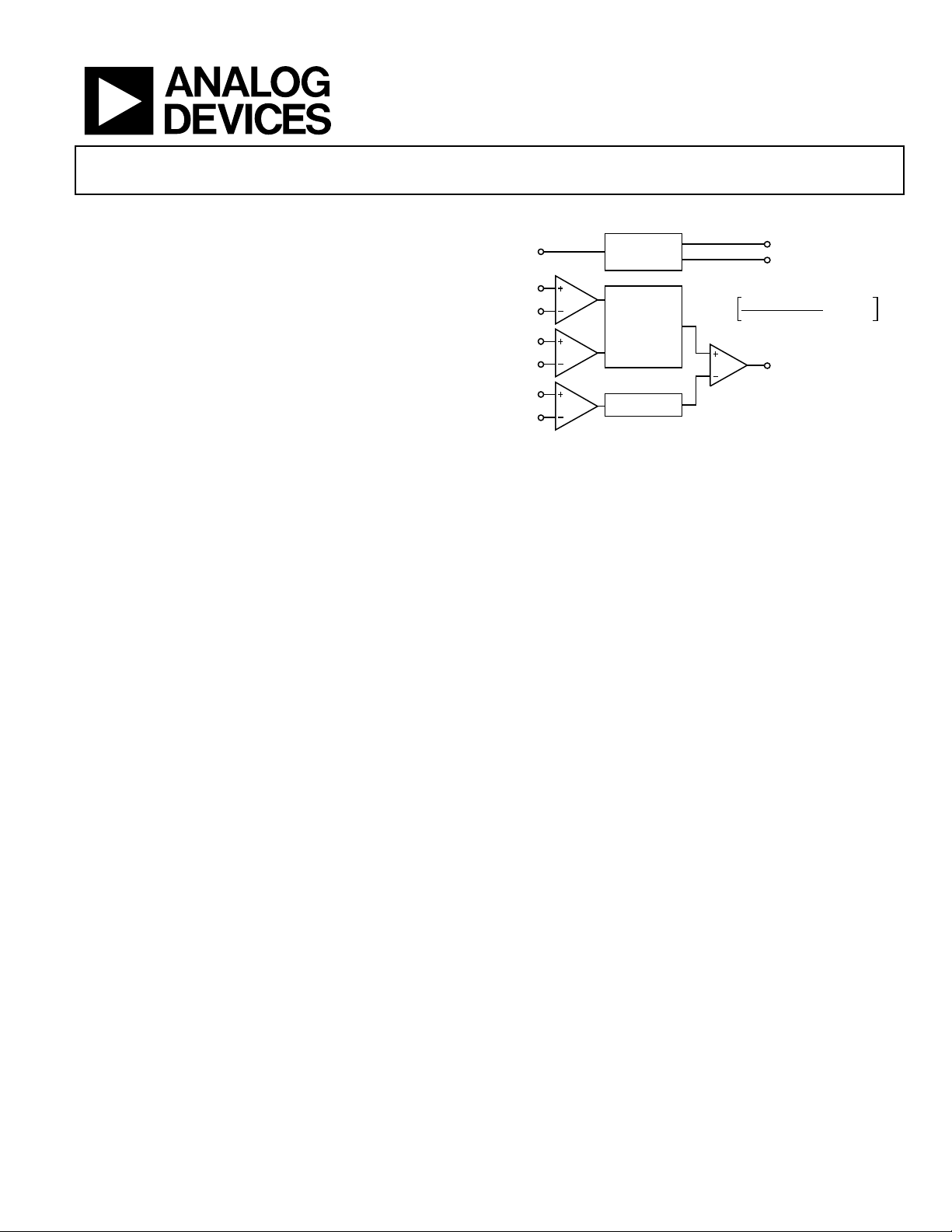
FUNCTIONAL BLOCK DIAGRAM
STABLE
SF
X
1
V-TO-1
X
2
Y
1
V-TO-1
Y
2
Z
1
V-TO-1
Z
2
REFERENCE
AND BIAS
TRANSLINEAR
MULTIPLIER
ELEMENT
0.75 AT TEN
TRANSFER FUNCT ION
V
= A
OUT
A
Figure 1.
standard value of 10.00 V; by means of an external resistor, this
can be reduced to values as low as 3 V.
The wide spectrum of applications and the availability of several
grades commend this multiplier as the first choice for all new
designs. The AD534J (±1% maximum error), AD534K (±0.5%
maximum), and AD534L (±0.25% maximum) are specified for
operation over the 0°C to +70°C temperature range. The AD534S
(±1% maximum) and AD534T (±0.5% maximum) are specified
over the extended temperature range, −55°C to +125°C. All
grades are available in hermetically sealed TO-100 metal cans
and SBDIP packages. AD534K, AD534S, and AD534T chips are
also available.
– X2) (Y1 – Y2)
(X
1
HIGH GAIN
OUTPUT
AMPLIFIER
+V
–V
SF
OUT
S
S
– Z2)
– (Z
1
09675-006
Rev. C
Information furnished by Analog Devices is believed to be accurate and reliable. However, no
responsibility is assumed by Analog Devices for its use, nor for any infringements of patents or other
rights of third parties that may result from its use. Specifications subject to change without notice. No
license is granted by implication or otherwise under any patent or patent rights of Analog Devices.
Trademarks and registered trademarks are the property of their respective owners.
One Technology Way, P.O. Box 9106, Norwood, MA 02062-9106, U.S.A.
Tel: 781.329.4700 www.analog.com
Fax: 781.461.3113 ©1977–2011 Analog Devices, Inc. All rights reserved.

AD534
TABLE OF CONTENTS
Features.............................................................................................. 1
Applications....................................................................................... 1
Functional Block Diagram .............................................................. 1
General Description ......................................................................... 1
Revision History ............................................................................... 2
Specifications..................................................................................... 3
Absolute Maximum Ratings............................................................ 7
Thermal Resistance ...................................................................... 7
ESD Caution.................................................................................. 7
Pin Configurations and Function Descriptions ........................... 8
Typical Performance Characteristics ........................................... 10
REVISION HISTORY
4/11—Rev. B to Rev. C
Changes to Features Section, Figure 1, and
General Description Section ........................................................... 1
Added Pin Configurations and Function Descriptions
Section................................................................................................ 8
Moved Provides Gain with Low Noise Section .......................... 12
Moved Unprecedented Flexibility Section .................................. 14
Updated Outline Dimensions....................................................... 17
Changes to Ordering Guide.......................................................... 18
Functional Description.................................................................. 12
Provides Gain with Low Noise ..................................................... 12
Operation as a Multiplier.......................................................... 12
Operation as a Squarer .............................................................. 13
Operation as a Divider............................................................... 13
Operation as a Square Rooter................................................... 14
Unprecedented Flexibility......................................................... 14
Applications Information.............................................................. 15
Outline Dimensions....................................................................... 17
Ordering Guide .......................................................................... 18
Rev. C | Page 2 of 20

AD534
−
−
−
SPECIFICATIONS
TA = 25°C, ±VS = ±15 V, R ≥ 2 kΩ, all minimum and maximum specifications are guaranteed, unless otherwise noted.
Table 1.
AD534J AD534K AD534L
Parameter Min Typ Max Min Typ Max Min Typ Max Unit
MULTIPLIER PERFORMANCE
Transfer Function
−
))((
YYXX
2121
Z
+
V10
2
))((
YYXX
2121
Z
+
V10
2
YYXX
−−
))((
2121
V10
+
Tot al E r ror1 (−10 V ≤ X, Y ≤ +10 V) ±1.02 ±0.52 ±0.252 %
TA = T
MIN
to T
±1.5 ±1.0 ±0.5 %
MAX
Total Error vs. Temperature ±0.022 ±0.015 ±0.008 %/°C
Scale Factor Error
(SF = 10.000 V Nominal)3 ±0.25 ±0.1 ±0.1 %
Temperature Coefficient of
Scaling Voltage ±0.02 ±0.01 ±0.005 %/°C
Supply Rejection (±15 V ± 1 V) ±0.01 ±0.01 ±0.01 %
2
Nonlinearity, X (X = 20 V p-p,
±0.4 ±0.2 ±0.3
±0.10 ±0.122 %
Y = 10 V)
Nonlinearity, Y (Y = 20 V p-p, X = 10 V ±0.2 ±0.1 ±0.12 ±0.005 ±0.12 %
Feedthrough4, X (Y Nulled,
±0.3 ±0.15 ±0.3
2
±0.05 ±0.122 %
X = 20 V p-p 50 Hz)
2
Feedthrough4, Y (X Nulled,
±0.01 ±0.01 ±0.1
±0.003 ±0.12 %
Y = 20 V p-p, 50 Hz)
Output Offset Voltage ±5 ±302 ±2 ±152 ±2 ±102 mV
Output Offset Voltage Drift 200 100 100 μV/°C
DYNAMICS
Small Signal BW (V
1% Amplitude Error (C
Slew Rate (V
OUT
Settling Time (to 1%, D V
= 0.1 rms) 1 1 1 MHz
OUT
= 1000 pF) 50 50 50 kHz
LOAD
20 p-p) 20 20 20 V/μs
= 20 V) 2 2 2 μs
OUT
NOISE
Noise Spectral Density
SF = 10 V 0.8 0.8 0.8 μV/√Hz
SF = 3 V5 0.4 0.4 0.4 μV/√Hz
Wideband Noise
f = 10 Hz to 5 MHz 1 1 1 mV rms
f = 10 Hz to 10 kHz 90 90 90 μV rms
OUTPUT
Output Voltage Swing ±112 ±112 ±112 V
Output Impedance (f ≤ 1 kHz) 0.1 0.1 0.1 Ω
Output Short-Circuit Current
(RL = 0 Ω, TA = T
MIN
to T
) 30 30 30 mA
MAX
Amplifier Open-Loop Gain (f = 50 Hz) 70 70 70 dB
INPUT AMPLIFIERS (X, Y, and Z)6
Signal Voltage Range
Differential or Common Mode ±10 ±10 ±10 V
Operating Differential ±12 ±12 ±12 V
Offset Voltage (X, Y) ±5 ±202 ±2 ±102 ±2 ±102 mV
Offset Voltage Drift (X, Y) 100 50 50 μV/°C
Offset Voltage (Z) ±5 ±302 ±2 ±152 ±2 ±102 mV
Offset Voltage Drift (Z) 200 100 100 μV/°C
CMRR 602 80 702 90 702 90 dB
Z
2
Rev. C | Page 3 of 20

AD534
−
AD534J AD534K AD534L
Parameter Min Typ Max Min Typ Max Min Typ Max Unit
Bias Current 0.8 2.02 0.8 2.02 0.8 2.02 μA
Offset Current 0.1 0.1 0.05 0.22 μA
Differential Resistance 10 10 10 MΩ
DIVIDER PERFORMANCE
Transfer Function (X1 > X2)
V10
)(
ZZ
12
+
Y
−−)(
1
XX
21
ZZ
)(
12
V10
+
Y
−
1
XX
)(
21
V10
)(
ZZ
12
+
Y
−−)(
1
XX
21
Tot al E r ror1
X = 10 V, −10 V ≤ Z ≤ +10 V ±0.75 ±0.35 ±0.2 %
X = 1 V, −1 V ≤ Z ≤ +1 V ±2.0 ±1.0 ±0.8 %
0.1 V ≤ X ≤ 10 V, −10 V ≤ Z ≤ +10 V ±2.5 ±1.0 ±0.8 %
SQUARER PERFORMANCE
Transfer Function
2
−
)(
21
ZXX+
V10
2
2
−
)(
21
ZXX+
V10
2
2
−
)(
21
ZXX+
V10
2
Total Error (−10 V ≤ X ≤ +10 V) ±0.6 ±0.3 ±0.2 %
SQUARE-ROOTER PERFORMANCE
Transfer Function (Z1 ≤ Z2) √(10 V(Z2 – Z1)) + X2 √(10 V(Z2 – Z1)) + X
2
√(10 V(Z
– Z1)) + X
2
Tot al E r ror1 (1 V ≤ Z ≤ 10 V) ±1.0 ±0.5 ±0.25 %
POWER SUPPLY SPECIFICATIONS
Supply Voltage
Rated Performance ±15 ±15 ±15 V
Operating ±8 ±182 ±8 ±182 ±8 ±182 V
Supply Current
Quiescent 4 62 4 62 4 62 mA
1
Specifications given are percent of full scale, ±10 V (that is, 0.01% = 1 mV).
2
Tested on all production units at final electrical test. Results from those tests are used to calculate outgoing quality levels.
3
Can be reduced down to 3 V using external resistor between –VS and SF.
4
Irreducible component due to nonlinearity; excludes effect of offsets.
5
Using external resistor adjusted to give SF = 3 V.
6
See for definition of sections. Figure 1
2
Rev. C | Page 4 of 20

AD534
−
−
TA = 25°C, ±VS = ±15 V, R ≥ 2 kΩ, all minimum and maximum specifications are guaranteed, unless otherwise noted.
Table 2.
AD534S AD534T
Parameter Min Typ Max Min Typ Max Unit
MULTIPLIER PERFORMANCE
Transfer Function
))((
YYXX
2121
Z
+
V10
2
YYXX
−−
))((
2121
Z
V10
+
Tot al E r ror1 (−10 V ≤ X, Y ≤ +10 V) ±1.02 ±0.52 %
TA = T
MIN
to T
±2.02 ±1.0 %
MAX
Total Error vs. Temperature ±0.022 ±0.012 %/°C
Scale Factor Error
(SF = 10.000 V Nominal)3 ±0.25 ±0.1 %
Temperature Coefficient of Scaling Voltage ±0.02 ±0.01 %/°C
Supply Rejection (±15 V ± 1 V) ±0.01 ±0.01 %
Nonlinearity, X (X = 20 V p-p, Y = 10 V) ±0.4 ±0.2 ±0.32 %
Nonlinearity, Y (Y = 20 V p-p, X = 10 V ±0.2 ±0.1 ±0.12 %
Feedthrough4, X (Y Nulled,
X = 20 V p-p, 50 Hz) ±0.3 ±0.15 ±0.32 %
Feedthrough4, Y (X Nulled,
Y = 20 V p-p, 50 Hz) ±0.01 ±0.01 ±0.12 %
Output Offset Voltage ±5 ±302 ±2 ±152 mV
Output Offset Voltage Drift 5002 3002 μV/°C
DYNAMICS
Small Signal BW (V
1% Amplitude Error (C
Slew Rate (V
OUT
Settling Time (to 1%, ΔV
= 0.1 rms) 1 1 MHz
OUT
= 1000 pF) 50 50 kHz
LOAD
20 p-p) 20 20 V/μs
= 20 V) 2 2 μs
OUT
NOISE
Noise Spectral Density
SF = 10 V 0.8 0.8 μV/√Hz
SF = 3 V5 0.4 0.4 μV/√Hz
Wideband Noise
f = 10 Hz to 5 MHz 1 1 mV/rms
f = 10 Hz to 10 kHz 90 90 μV/rms
OUTPUT
Output Voltage Swing ±112 ±112 V
Output Impedance (f ≤ 1 kHz) 0.1 0.1 Ω
Output Short-Circuit Current (RL = 0 Ω, TA = T
MIN
to T
) 30 30 mA
MAX
Amplifier Open-Loop Gain (f = 50 Hz) 70 70 dB
INPUT AMPLIFIERS (X, Y, and Z)6
Signal Voltage Range
Differential or Common Mode ±10 ±10 V
Operating Differential ±12 ±12 V
Offset Voltage (X, Y) ±5 ±202 ±2 ±102 mV
Offset Voltage Drift (X, Y) 100 150 μV/°C
Offset Voltage (Z) ±5 ±302 ±2 ±152 mV
Offset Voltage Drift (Z) 5002 3002 μV/°C
CMRR 602 80 702 90 dB
Bias Current 0.8 2.02 0.8 2.02 μA
Offset Current 0.1 0.1 μA
Differential Resistance 10 10 MΩ
2
Rev. C | Page 5 of 20

AD534
−
AD534S AD534T
Parameter Min Typ Max Min Typ Max Unit
DIVIDER PERFORMANCE
Transfer Function (X1 > X2)
ZZ
)(
12
V10
+
Y
−
1
XX
)(
21
V10
)(
ZZ
12
+
Y
−−)(
1
XX
21
Tot al E r ror1
X = 10 V, −10 V ≤ Z ≤ +10 V ±0.75 ±0.35 %
X = 1 V, −1 V ≤ Z ≤ +1 V ±2.0 ±1.0 %
0.1 V ≤ X ≤ 10 V, −10 V ≤ Z ≤ +10 V ±2.5 ±1.0 %
SQUARER PERFORMANCE
Transfer Function
2
−
)(
21
ZXX+
V10
2
2
−
)(
21
ZXX+
V10
2
Total Error (−10 V ≤ X ≤ +10 V) ±0.6 ±0.3 %
SQUARE-ROOTER PERFORMANCE
Transfer Function (Z1 ≤ Z2) √(10 V(Z2 – Z1)) + X2 √(10 V(Z2 – Z1)) + X2
Tot al E r ror1 (1 V ≤ Z ≤ 10 V) ±1.0 ±0.5 %
POWER SUPPLY SPECIFICATIONS
Supply Voltage
Rated Performance ±15 ±15 V
Operating ±8 ±222 ±8 ±222 V
Supply Current
Quiescent 4 62 4 62 mA
1
Specifications given are percent of full scale, ±10 V (that is, 0.01% = 1 mV).
2
Tested on all production units at final electrical test. Results from those tests are used to calculate outgoing quality levels.
3
Can be reduced down to 3 V using external resistor between –VS and SF.
4
Irreducible component due to nonlinearity: excludes effect of offsets.
5
Using external resistor adjusted to give SF = 3 V.
6
See for definition of sections. Figure 1
Rev. C | Page 6 of 20

AD534
V
X
5
ABSOLUTE MAXIMUM RATINGS
Table 3.
AD534J,
Parameter
AD534L
Supply Voltage ±18 V ±22 V
Internal Power Dissipation 500 mW 500 mW
Output Short Circuit to
Ground Indefinite Indefinite
Input Voltages (X1, X2, Y1, Y2,
AD534K,
, Z2) ±VS ±VS
Z
1
Rated Operating
Temperature Range 0°C to +70°C −55°C to +125°C
Storage Temperature
Range −65°C to +150°C −65°C to +150°C
Lead Temperature Range,
60 sec Soldering 300°C 300°C
Stresses above those listed under Absolute Maximum Ratings
may cause permanent damage to the device. This is a stress
rating only; functional operation of the device at these or any
other conditions above those indicated in the operational
section of this specification is not implied. Exposure to absolute
maximum rating conditions for extended periods may affect
device reliability.
THERMAL RESISTANCE
θJA is specified for the worst-case conditions, that is, a device
soldered in a circuit board for surface-mount packages.
Table 4. Thermal Resistance
Package Type θJA θ
10-Pin TO-100 (H-10) 150 25 °C/W
14-Lead SBDIP (D-14) 95 25 °C/W
20-Terminal LCC (E-20-1) 95 25 °C/W
AD534S,
AD534T
Unit
JC
+
1
X
2
SF
Y
1
Y
2
S
0.100 (2.54)
5
3
4
8
A
–V
S
Figure 2. Chip Dimensions and Bonding Diagram
Dimensions shown in inches and (mm)
Contact factory for latest dimensions.
+V
S
0kΩ
470kΩ
–V
S
1kΩ
TO APPROP RIATE
INPUT TERMINAL
Figure 3. Optional Trimming Configuration
ESD CAUTION
OUT
Z
09675-005
0.076
(1.93)
Z
1
2
09675-004
Rev. C | Page 7 of 20

AD534
V
PIN CONFIGURATIONS AND FUNCTION DESCRIPTIONS
+
S
X1
10
X2
1
TOP VIEW
2
SF
Y1
Figure 4. TO-100 (H-10) Pin Configuration
Table 5. H-10 Package Pin Function Descriptions
Pin No. Mnemonic Description
1 X2 Inverting Differential Input of the X Multiplicand Input.
2 SF Scale Factor Input.
3 Y1 Noninverting Differential Input of the Y Multiplicand Input.
4 Y2 Inverting Differential Input of the Y Multiplicand Input.
5 −VS Negative Supply Rail.
6 Z2 Inverting Differential Input of the Z Reference Input.
7 Z1 Noninverting Differential Input of the Z Reference Input.
8 OUT Product Output.
9 +VS Positive Supply Rail.
10 X1 Noninverting Differential Input of the X Multiplicand Input.
9
AD534
(Not to
Scale)
3
4
Y2
OUT
8
Z1
7
6
Z2
5
–V
S
09675-001
1
X1
2
X2
3
NC
NC
AD534
TOP VIEW
4
SF
(Not to Scale)
5
Y1
6
Y2
7
NC = NO CONNECT. DO NOT
CONNECT TO T HIS PIN.
14
+V
S
13
NC
12
OUT
11
Z1
10
Z2
NC
9
8
–V
S
09675-002
Figure 5. TO-100 (D-14) Pin Configuration
Table 6. D-14 Package Pin Function Descriptions
Pin No. Mnemonic Description
1 X1 Noninverting Differential Input of the X Multiplicand Input.
2 X2 Inverting Differential Input of the X Multiplicand Input.
3, 5, 9, 13 NC No Connect. Do not connect to this pin.
4 SF Scale Factor Input.
6 Y1 Noninverting Differential Input of the Y Multiplicand Input.
7 Y2 Inverting Differential Input of the Y Multiplicand Input.
8 −VS Negative Supply Rail.
10 Z2 Inverting Differential Input of the Z Reference Input.
11 Z1 Noninverting Differential Input of the Z Reference Input.
12 OUT Product Output.
14 +VS Positive Supply rail.
Rev. C | Page 8 of 20

AD534
X2
4
NC
5
NC
6
SF
NC
NC
(Not to Scale)
7
8
Y1
NC = NO CONNECT . DO NOT
CONNECT TO THIS PIN.
1NC2X13
AD534
TOP VIEW
11NC10Y29
S
+V
19NC20
18
OUT
17
NC
16
Z1
15
NC
14
Z2
13NC12
S
–V
09675-003
Figure 6. LCC (E-20-1) Pin Configuration
Table 7. E-20-1 Package Pin Function Descriptions
Pin No. Mnemonic Description
1, 4, 5, 7, 8, 11, 13, 15, 17, 19 NC No Connect. Do not connect to this pin.
2 X1 Noninverting Differential Input of the X Multiplicand Input.
3 X2 Inverting Differential Input of the X Multiplicand Input.
6 SF Scale Factor Input.
9 Y1 Noninverting Differential Input of the Y Multiplicand Input.
10 Y2 Inverting Differential Input of the Y Multiplicand Input.
12 −VS Negative Supply Rail.
14 Z2 Inverting Differential Input of the Z Reference Input.
16 Z1 Noninverting Differential Input of the Z Reference Input.
19 OUT Product Output.
20 +VS Positive Supply Rail.
Rev. C | Page 9 of 20

AD534
TYPICAL PERFORMANCE CHARACTERISTICS
Typical at 25°C, with ±VS = ±15 V dc, unless otherwise noted.
14
OUTPUT, RL ≥ 2kΩ
12
10
8
6
PEAK POSITIVE OR NEGATIVE SIGNAL (V)
4
8 10121416182
POSITIVE OR NEGATIVE SUPPLY (V)
ALL INPUTS, SF = 10V
Figure 7. Input/Output Signal Range vs. Supply Voltages
0
09675-020
1000
100
10
FEEDTHRO UGH (mV p- p)
0.1
X-FEEDTHRO UGH
1
Y-FEEDTHROUGH
10 100 1k 10k 100k 1M 10M
FREQUENCY (Hz)
Figure 10. AC Feedthrough vs. Frequency
09675-023
800
700
600
500
400
300
BIAS CURRENT (nA)
200
100
0
–60 –40 –20 0 20 40 60 80 100 120 140
SCALING V OLTAG E = 10V
SCALING VOLTAGE = 3V
TEMPERAT URE (°C)
Figure 8. Bias Current vs. Temperature (X, Y, or Z Input)
90
80
70
60
50
40
CMRR (dB)
30
20
10
0
100 1k 10k 100k 1M
TYPICAL FOR
ALL INPUTS
FREQUENCY ( Hz)
Figure 9. Common-Mode Rejection Ratio vs. Frequency
1.5
1
0.5
NOISE SPECTRAL DENSITY (µV/ Hz)
0
10 100 1k 10 k 100k
09675-021
SCALING V OLTAG E = 10V
SCALING VOLTAG E = 3V
FREQUENCY ( Hz)
09675-024
Figure 11. Noise Spectral Density vs. Frequency
100
90
CONDITIONS:
80
70
60
OUTPUT NOISE VOLTAGE (µV rms)
50
09675-022
2.5 5.0 7.5 10.0
10Hz TO 10kHz BANDWIDTH
SCALING VOLTAGE, SF (V)
09675-025
Figure 12. Wideband Noise vs. Scaling Voltage
Rev. C | Page 10 of 20

AD534
10
0dB = 0.1V RMS, RL = 2kΩ
60
0
CL = 0pF
–10
OUTPUT RESPONSE (dB)
–20
–30
10k
C
≤ 1000pF
L
C
= 0pF
F
FEEDBACK
ATTENUATO R
100k
FREQUENCY (Hz )
CL ≤ 1000pF
C
≤ 200pF
F
WITH ×10
1M 10M
NORMAL
CONNECTIO N
09675-026
Figure 13. Frequency Response as a Multiplier
40
Z
VOV
( )
20
OUTPUT – dB
0
–20
1k 10k 100k
VX = 100mV dc
V
= 10mV rms
Z
FREQUENCY (Hz)
V
= 1V dc
X
V
= 100mV rms
Z
= 10V dc
V
X
V
= 1V rms
Z
1M 10M
Figure 14. Frequency Response vs. Divider Denominator Input Voltage
09675-027
Rev. C | Page 11 of 20

AD534
±
K
Y
±
K
FUNCTIONAL DESCRIPTION
Figure 1 shows a functional block diagram of the AD534. Inputs
are converted to differential currents by three identical voltageto-current converters, each trimmed for zero offset. The product
of the X and Y currents is generated by a multiplier cell using
Gilbert’s translinear technique. An on-chip buried Zener
provides a highly stable reference, which is laser trimmed to
provide an overall scale factor of 10 V. The difference between
XY/SF and Z is then applied to the high gain output amplifier.
This permits various closed-loop configurations and dramatically reduces nonlinearities due to the input amplifiers, a
dominant source of distortion in earlier designs.
The effectiveness of the new scheme can be judged from the
fact that, under typical conditions as a multiplier, the nonlinearity on the Y input, with X at full scale (±10 V), is ±0.005% of FS.
Even at its worst point, which occurs when X = ±6.4 V, nonlinearity is typically only ±0.05% of FS. Nonlinearity for signals applied
to the X input, on the other hand, is determined almost entirely
by the multiplier element and is parabolic in form. This error is a
major factor in determining the overall accuracy of the unit and
therefore is closely related to the device grade.
The generalized transfer function for the AD534 is given by
OUT
()()
AV
=
SF
YYXX
−−
2121
()
−−
ZZ
21
where:
A is the open-loop gain of the output amplifier, typically
70 dB at dc.
X
, Y1, Z1, X2, Y2, and Z2 are the input voltages (full scale = ±SF,
1
peak = ±1.25 SF).
SF is the scale factor, pretrimmed to 10.00 V but adjustable by
the user down to 3 V.
In most cases, the open-loop gain can be regarded as infinite,
and SF is 10 V. The operation performed by the AD534, can
then be described in terms of the following equation:
(X
− X2)(Y1 −Y2 ) = 10 V (Z1 − Z2)
1
The user can adjust SF for values between 10.00 V and 3 V by
connecting an external resistor in series with a potentiometer
between SF and −V
. The approximate value of the total
S
resistance for a given value of SF is given by the relationship:
R
S
F
Due to device tolerances, allowance should be made to vary R
SF
k4.5
SF
−=01
SF
by ±25% using the potentiometer. Considerable reduction in
bias currents, noise, and drift can be achieved by decreasing SF.
This has the overall effect of increasing signal gain without the
customary increase in noise. Note that the peak input signal is
always limited to 1.25 SF (that is, ±5 V for SF = 4 V) so the
overall transfer function shows a maximum gain of 1.25. The
performance with small input signals, however, is improved by
using a lower scale factor because the dynamic range of the
Rev. C | Page 12 of 20
inputs is now fully utilized. Bandwidth is unaffected by the use
of this option.
Supply voltages of ±15 V are generally assumed. However,
satisfactory operation is possible down to ±8 V (see Figure 7).
Because all inputs maintain a constant peak input capability of
±1.25 SF, some feedback attenuation is necessary to achieve
output voltage swings in excess of ±12 V when using higher
supply voltages.
PROVIDES GAIN WITH LOW NOISE
The AD534 is the first general-purpose multiplier capable of
providing gains up to ×100, frequently eliminating the need for
separate instrumentation amplifiers to precondition the inputs.
The AD534 can be very effectively employed as a variable gain
differential input amplifier with high common-mode rejection.
The gain option is available in all modes and simplifies the
implementation of many function-fitting algorithms such as
those used to generate sine and tangent. The utility of this
feature is enhanced by the inherent low noise of the AD534:
90 µV rms (depending on the gain), a factor of 10 lower than
previous monolithic multipliers. Drift and feedthrough are also
substantially reduced over earlier designs.
OPERATION AS A MULTIPLIER
Figure 15 shows the basic connection for multiplication. Note
that the circuit meets all specifications without trimming.
+V
X
X INPUT
±10V FS
12V P
INPUT
±10V FS
12V P
1
X
2
OUT
AD534
SF
Y
1
Y
2
Figure 15. Basic Multiplier Connection
To reduce ac feedthrough to a minimum (as in a suppressed
carrier modulator), apply an external trim voltage (±30 mV
range required) to the X or Y input (see Figure 3). Figure 10
shows the typical ac feedthrough with this adjustment mode.
Note that the Y input is a factor of 10 lower than the X input
and should be used in applications where null suppression is
critical.
The high impedance Z
terminal of the AD534 can be used to
2
sum an additional signal into the output. In this mode, the
output amplifier behaves as a voltage follower with a 1 MHz
small signal bandwidth and a 20 V/µs slew rate. This terminal
should always be referenced to the ground point of the driven
system, particularly if this is remote. Likewise, the differential
inputs should be referenced to their respective ground potentials to realize the full accuracy of the AD534.
A much lower scaling voltage can be achieved without any
reduction of input signal range using a feedback attenuator as
shown in Figure 16. In this example, the scale is such that V
+15V
S
OUTPUT, ±12V PK =
(X1 – X
) (Y1 – Y2)
2
Z
1
Z
2
–15V
–V
S
10V
OPTIO NAL SUMMING
INPUT, Z, ±10V PK
+ Z
2
OUT
09675-007
=

AD534
K
K
(X1 – X2)(Y1 – Y2), so that the circuit can exhibit a maximum
gain of 10. This connection results in a reduction of bandwidth
to about 80 kHz without the peaking capacitor C
= 200 pF. In
F
addition, the output offset voltage is increased by a factor of 10
making external adjustments necessary in some applications.
Adjustment is made by connecting a 4.7 MΩ resistor between
Z
and the slider of a potentiometer connected across the
1
supplies to provide ±300 mV of trim range at the output.
X INPUT
±10V FS
±12V P
Y INPUT
±10V FS
±12V P
X
1
X
2
AD534
SF
Y
1
Y
2
OUT
+15V
S
OUTPUT , ±12V PK =
(X
– X2) (Y1 – Y2)
1
90kΩ
Z
1
10kΩ
Z
2
–15V
–V
S
(SCALE = 1V )
OPTIO NAL PEAKING
CAPACITOR C
= 200pF
F
09675-008
+V
Figure 16. Connections for Scale Factor of Unity
Feedback attenuation also retains the capability for adding a
signal to the output. Signals can be applied to the high impedance
Z
terminal where they are amplified by +10 or to the common
2
ground connection where they are amplified by +1. Input signals
can also be applied to the lower end of the 10 kΩ resistor, giving
a gain of −9. Other values of feedback ratio, up to ×100, can be
used to combine multiplication with gain.
Occasionally, it may be desirable to convert the output to a
current into a load of unspecified impedance or dc level. For
example, the function of multiplication is sometimes followed
by integration; if the output is in the form of a current, a simple
capacitor provides the integration function. Figure 17 shows
how this can be achieved. This method can also be applied in
squaring, dividing, and square rooting modes by appropriate
choice of terminals. This technique is used in the voltage
controlled low-pass filter and the differential input voltage-tofrequency converter shown in the Applications Information
section.
X INPUT
±10V FS
±12V PK
Y INPUT
±10V FS
±12V PK
X
1
X
2
SF
Y
1
Y
2
AD534
OUT
–V
S
Z
1
Z
2
S
CURRENT-SENSING
RESISTOR, RS, 2kΩ MIN
– X2) (Y1 – Y2)
(X
1
I
=×
OUT
10V
INTEGRATOR
CAPACITOR
(SEE TEXT)
1
RS
+V
Figure 17. Conversion of Output to Current
OPERATION AS A SQUARER
Operation as a squarer is achieved in the same fashion as the
multiplier except that the X and Y inputs are used in parallel.
The differential inputs can be used to determine the output
polarity (positive for X
of the inputs is reversed). Accuracy in the squaring mode is
typically a factor of 2 better than in the multiplying mode and
the largest errors occurring with small values of output for
input below 1 V.
= Yl and X2 = Y2, negative if either one
1
9675-009
If the application depends on accurate operation for inputs that
are always less than ±3 V, the use of a reduced value of SF is recommended as described in the Functional Description section.
Alternatively, a feedback attenuator can be used to raise the
output level. This is put to use in the difference-of-squares
application to compensate for the factor of 2 loss involved in
generating the sum term (see Figure 20).
The difference of squares function is also used as the basis for a
novel rms-to-dc converter shown in Figure 27. The averaging
filter is a true integrator, and the loop seeks to zero its input. For
this to occur, (V
well below the averaging time constant). Therefore, V
forced to equal the rms value of V
)2 − (V
IN
)2 = 0 V (for signals whose period is
OUT
OUT
. The absolute accuracy of
IN
is
this technique is very high; at medium frequencies and for
signals near full scale, it is determined almost entirely by the
ratio of the resistors in the inverting amplifier. The multiplier
scaling voltage affects only open-loop gain. The data shown is
typical of performance that can be achieved with an AD534K,
but even using an AD534J, this technique can readily provide
better than 1% accuracy over a wide frequency range, even for
crest factors in excess of 10.
OPERATION AS A DIVIDER
Figure 18 shows the connection required for division. Unlike
earlier products, the AD534 provides differential operation on
both numerator and denominator, allowing the ratio of two
floating variables to be generated. Further flexibility results
from access to a high impedance summing input to Y
all dividers based on the use of a multiplier in a feedback loop,
the bandwidth is proportional to the denominator magnitude,
as shown in Figure 14.
X INPUT
(DENOMINATOR)
±10V FS
±12V PK
OPTIONAL
SUMMING
INPUT
±10V PK
+
–
X
1
X
2
AD534
SF
Y
1
Y
2
+V
OUT
–V
+15V
S
Z
1
Z
2
–15V
S
Figure 18. Basic Divider Connection
OUTPUT, ±12V PK =
Z INPUT
(NUMERATOR)
±10V FS
±12V PK
Without additional trimming, the accuracy of the AD534K and
AD534L is sufficient to maintain a 1% error over a 10 V to 1 V
denominator range. This range can be extended to 100:1 by
simply reducing the X offset with an externally generated trim
voltage (range required is ±3.5 mV maximum) applied to the
unused X input (see Figure 3). To trim, apply a ramp of +100 mV
to +V at 100 Hz to both X
and Z1 (if X2 is used for offset adjust-
1
ment; otherwise, reverse the signal polarity) and adjust the trim
voltage to minimize the variation in the output
Because the output is near 10 V, it should be ac-coupled for
this adjustment. The increase in noise level and reduction in
bandwidth preclude operation much beyond a ratio of 100 to 1.
10V (Z
(X
. As with
1
– Z1)
2
– X2)
1
+ Y
1
09675-010
Rev. C | Page 13 of 20

AD534
X
As with the multiplier connection, overall gain can be introduced
by inserting a simple attenuator between the output and Y
2
terminal. This option and the differential ratio capability of the
AD534 are used in the percentage computer application shown
in Figure 24. This configuration generates an output proportional to the percentage deviation of one variable (A) with
respect to a reference variable (B), with a scale of 1% per volt.
OPERATION AS A SQUARE ROOTER
The operation of the AD534 in the square root mode is shown
in Figure 19. The diode prevents a latching condition, which
may occur if the input momentarily changes polarity. As shown,
the output is always positive; it can be changed to a negative
output by reversing the diode direction and interchanging the X
inputs. Because the signal input is differential, all combinations
of input and output polarities can be realized, but operation is
restricted to the one quadrant associated with each combination
of inputs.
OUTPUT, ±12V PK =
10V (Z
– Z1) + X
2
R
L
(MUST BE
PROVIDED)
OPTIO NAL
SUMMING
INPUT
, ±10V PK
X
1
X
2
AD534
SF
Y
1
Y
2
+V
OUT
–V
S
Z
1
Z
2
S
+15V
–
+
–15V
Z INPUT
±10V FS
±12V PK
REVERSE THIS
AND X INPUTS
FOR NEGAT IVE
OUTPUTS
Figure 19. Square-Rooter Connection
2
09675-011
In contrast to earlier devices, which were intolerant of capacitive
loads in the square root modes, the AD534 is stable with all
loads up to at least 1000 pF. For critical applications, a small
adjustment to the Z input offset (see Figure 3) improves
accuracy for inputs below 1 V.
UNPRECEDENTED FLEXIBILITY
The precise calibration and differential Z input provide a degree
of flexibility found in no other currently available multiplier.
Standard multiplication, division, squaring, square-rooting
(MDSSR) functions are easily implemented while the restriction
to particular input/output polarities imposed by earlier designs
has been eliminated. Signals can be summed into the output,
with or without gain and with either a positive or negative
sense. Many new modes based on implicit function synthesis
have been made possible, usually requiring only external
passive components. The output can be in the form of a current,
if desired, facilitating such operations as integration.
Rev. C | Page 14 of 20

AD534
A
–
E
2
3
4
θ
C
V
APPLICATIONS INFORMATION
The versatility of the AD534 allows the creative designer to implement a variety of circuits such as wattmeters, frequency doublers, and
automatic gain controls.
+V
+V
X
1
A – B
2
X
2
OUT
AD534
SF
Y
1
A + B
B
2
Y
–V
2
+15V
S
OUTPUT =
30kΩ
Z
1
10kΩ
Z
2
–15V
S
Figure 20. Difference of Squares
+V
X
2kΩ
1
X
2
AD534
SF
Y
1
Y
2
C
OUT
, ZERO TO × 50.
CONTROL I NPUT,
, 0V TO ±5V
E
C
SET GAIN
1kΩ
V
S
SIGNAL INPUT,
, ±5V PK
E
S
NOTES
1. GAIN IS × 10 PER VOLT OF
. WIDEBAN D (10Hz TO 30kHz) OUT PUT NOI SE IS 3mV rms,
TYP CORRESPONDING TO A.F.S. SNR OF 70dB.
. NOISE REFERRED TO SIGNAL INPUT, WITH EC = ±5V, IS
60µV rms, TYP.
. BANDWIDTH IS DC TO 20kHz, –3dB, INDEPENDENT OF GAIN.
+15V
S
OUTPUT , ±12V PK =
39kΩ
Z
1
1kΩ
Z
2
–V
S
0.005µF
–15V
Figure 21. Voltage-Controlled Amplifier
X
MODULATION
INPUT, ±E
M
1
X
2
OUT
AD534
2
2
A
10V
– B
09675-012
ARRIER INP UT
sin ωt
E
C
THE SF PIN OR A Z ATT ENUATOR CAN BE USED TO PROVIDE O VERALL
SIGNAL AMPLIFICATION. OPERATION FROM A SINGLE SUPPLY POSSIBLE;
TO VS/2.
BIAS Y
2
SF
Y
1
Y
2
Figure 23. Linear AM Modulator
E
C ES
0.1V
9kΩ
1kΩ
B INPUT,
(+
ONLY)
E
09675-013
OTHER SCALES, FROM 10% PER VOLT TO 0.1% PER VOLT
CAN BE OBTAINED BY ALTE RING THE FEEDBACK RATI O.
X
1
X
2
AD534
SF
Y
1
Y
2
+V
OUT
–V
S
Z
Z
S
Figure 24. Percentage Computer
+15V
S
E
OUTPUT = 1 ± EC sin ωt
Z
1
Z
2
–15V
–V
S
10V
M
+15V
OUTPUT = (100V)
(1% PER VOLT)
1
2
A INPU T (± )
A – B
B
–15V
09675-015
09675-016
INPUT, E
0V TO +10V
+V
X
1
X
2
18kΩ
10kΩ
θ
USING CL OSE TOLERANCE R ESISTORS AND AD543L ,
ACCURACY OF F IT I S WIT HIN ±0.5% AT ALL P OINT S.
θ IS IN RADIANS.
AD534
SF
Y
1
Y
2
OUT
–V
+15V
S
Z
Z
4.7kΩ
1
4.3kΩ
2
–15V
S
3kΩ
Figure 22. Sine Function Generator
OUTPUT = (10V) sin
WHERE θ = ×
π
10V
2
+V
X
E
θ
1
X
2
OUT
AD534
SF
INPUT, Y ±10V FS
09675-014
Y
1
Y
2
+15V
S
OUTPUT, ±5V/PK =
y
(10V)
Z
1
Z
2
–15V
–V
S
1 + y
WHERE y =
Y
(10V)
09675-017
Figure 25. Bridge Linearization Function
Rev. C | Page 15 of 20

AD534
C
±
K
A
%
ADJ 8kHz
39kΩ
+V
ONTROL INPUT,
E
100mV TO 10V
C
X
1
X
2
OUT
AD534
SF
+
Y
1
–
Y
2
CALIBRATIO N PROCEDURE:
WITH E
= 1.0V, ADJUST POTENTIOMETER TO SET f = 1.000kHz WITH
C
E
= 8.0V, ADJUST TRIMMER CA PACITOR TO SET f = 8.000kHz. LINEARITY
C
WILL TYPICALLY BE WITHIN ±0.1% OF FS FORANY OTHER INPUT.
DUE TO DELAYS IN THE COMPARATOR, THIS TE CHNIQUE IS NOT SUITABLE
FOR MAXI MUM FREQ UENCIES ABOVE 10kHz. FOR FREQUENCI ES ABOVE
10kHz THE AD537 VO LTAGE-TO-FREQ UENCY CONVERTER IS RE COMMENDED.
A TRIANGLE-WAVE OF ±5V PK APPEARS ACRO SS THE 0.01µF CAPACITOR: IF
USED AS AN OUTPUT, A VOLTAGE -FOLL OWER SHOULD BE I NTERPOSED.
+15V
S
ADJ
Z
1
Z
2
–V
S
1kHz
500Ω
(= R)
–15V
2.2kΩ
0.01
(= C)
3pF to 30pF
2
3
AD211
PINS 5, 6, 8 TO +15V
PINS 1, 4 TO –15V
f = ×
WITH VALUES SHOWN
7
E
40
82kΩ
C
1
CR
+15V
2kΩ
OUTPUT
±15V APPROX.
= 1kHz PER VOLT
09675-018
Figure 26. Differential Input Voltage-to-Frequency Converter
M
TCHED TO 0.025
20kΩ 10kΩ 10kΩ
INPUT
5V RMS FS
10V PEA
RMS + DC
MODE
AC RMS
10µF
NONPOLAR
10kΩ
X
1
X
2
AD534
SF
Y
1
Y
2
20kΩ
+V
OUT
–V
AD741K
+15V
S
10kΩ
Z
1
10kΩ
Z
2
S
–15V
ZERO
ADJ
10MΩ
5kΩ
+
10µF SOLID Ta
AD741J
+15V
OUTPUT
0V TO 5V
CALIBRATIO N PROCEDURE:
WITH MODE SWITCH IN ‘RMS + DC’ POSITION, APPLY AN INPUT OF +1.00V DC.
ADJUST ZERO UNTIL OUTPUT READS SAME AS INPUT. CHECK FOR INPUTS
OF ±10V; OUTPUT SHOULD BE WITHIN ±0.05% (5mV).
ACCURACY I S MAINTAINED FRO M 60Hz TO 100kHz , AND IS TYPICALLY HIGH
BY 0.5% AT 1MHz FOR V
PROVIDED THAT THE PEAK INPUT IS NOT EXCEEDED, CREST FACTORS UP
TO AT LEAST 10 HAVE NO APPRECIABLE EF FECT ON ACCURACY.
INPUT IM PEDANCE IS ABOUT 10kΩ; F OR HIGH (10MΩ) IMPEDANCE, REMOVE
MODE SWI TCH AND INPUT COUPLI NG COMPONENTS.
FOR GUARANTEED SPECIFICATIONS THE AD536A AND AD636 ARE OFFERED
AS A SINGLE PACKAGE RMS-TO-DC CONVERT ER.
= 4V RMS (SINE, SQUARE, OR TRIANGLULAR-WAVE).
IN
09675-019
Figure 27. Wideband, High-Crest Factor, RMS-to-DC Converter
Rev. C | Page 16 of 20

AD534
C
OUTLINE DIMENSIONS
REFERENCE PLANE
0.185 (4.70)
0.165 (4.19)
0.370 (9.40)
0.335 (8.51)
0.335 (8.51)
0.040 (1.02) MAX
0.050 (1.27) MAX
0.500 (12.70)
MIN
0.021 (0.53)
0.016 (0.40)
0.305 (7.75)
BASE & SEATING PLANE
DIMENSI ONS PER JE DEC STANDARDS MO-006-AF
CONTROL LING DIMENSIONS ARE IN INCHES; MILLI METER DI MENSIO NS
(IN PARENT HESES) ARE ROUNDED-OFF INCH EQUIVALENTS FOR
REFERENCE O NLY AND ARE NOT APPROPRIATE F OR USE IN DESIGN.
0.115
(2.92)
BSC
0.230 (5.84)
BSC
0.160 (4.06)
0.110 (2.79)
5
4
3
2
6
7
8
0.045 (1.14)
9
0.025 (0.65)
1
10
36° BSC
0.034 (0.86)
0.025 (0.64)
022306-A
Figure 28. 10-Pin Metal Header Package [TO-100]
(H-10)
Dimensions shown in inches and (millimeters)
0.005 (0.13) MIN
PIN 1
0.200 (5.08)
MAX
0.200 (5.08)
0.125 (3.18)
0.023 (0.58)
0.014 (0.36)
0.080 (2.03) MAX
14
1
0.100 (2.54)
BSC
0.765 (19.43) MAX
0.070 (1.78)
0.030 (0.76)
8
7
0.310 (7.87)
0.220 (5.59)
0.060 (1.52)
0.015 (0.38)
0.150
(3.81)
MIN
SEATING
PLANE
0.320 (8.13)
0.290 (7.37)
0.015 (0.38)
0.008 (0.20)
ONTROLLING DIMENSIONS ARE IN INCHES; MILLIMETER DIMENSIONS
(IN PARENTHESES) ARE ROUNDED-OFF INCH EQUIVALENTS FOR
REFERENCE ONLY AND ARE NOT APPROPRIATE FOR USE IN DESIGN.
Figure 29. 14-Lead Side-Brazed Ceramic Dual In-Line Package [SBDIP]
(D-14)
Dimensions shown in inches and (millimeters)
1
VIEW
0.150 (3.81)
BSC
0.200 (5.08)
REF
0.100 (2.54) REF
0.015 (0.38)
MIN
3
4
0.028 (0.71)
0.022 (0.56)
0.050 (1.27)
8
BSC
9
45° TYP
022106-A
0.075 (1.91)
0.095 (2.41)
0.075 (1.90)
0.011 (0.28)
0.007 (0.18)
R TYP
0.075 (1.91)
REF
0.055 (1.40)
0.045 (1.14)
REF
19
18
14
13
20
BOTTOM
0.100 (2.54)
0.064 (1.63)
0.358 (9.09)
0.342 (8.69)
SQ
CONTROLL ING DIMENSI ONS ARE IN INCHES; MILLIME TER DIMENSIONS
(IN PARENTHESES) ARE ROUNDED-OF F INCH EQUI VALENTS FOR
REFERENCE ONLY AND ARE NOT APPROPRIATE FOR USE IN DESI GN.
0.358
(9.09)
MAX
0.088 (2.24)
0.054 (1.37)
SQ
Figure 30. 20-Terminal Ceramic Leadless Chip Carrier [LCC]
(E-20-1)
Dimensions shown in inches and (millimeters)
Rev. C | Page 17 of 20

AD534
ORDERING GUIDE
Model1 Temperature Range Package Description Package Option
AD534JD 0°C to +70°C 14-Lead Side Brazed Ceramic Dual In-Line Package [SBDIP] D-14
AD534JDZ 0°C to +70°C 14-Lead Side Brazed Ceramic Dual In-Line Package [SBDIP] D-14
AD534KD 0°C to +70°C 14-Lead Side Brazed Ceramic Dual In-Line Package [SBDIP] D-14
AD534KDZ 0°C to +70°C 14-Lead Side Brazed Ceramic Dual In-Line Package [SBDIP] D-14
AD534LD 0°C to +70°C 14-Lead Side Brazed Ceramic Dual In-Line Package [SBDIP] D-14
AD534LDZ 0°C to +70°C 14-Lead Side Brazed Ceramic Dual In-Line Package [SBDIP] D-14
AD534JH 0°C to +70°C 10-Pin Metal Header Package [TO-100] H-10
AD534JHZ 0° C to +70°C 10-Pin Metal Header Package [TO-100] H-10
AD534KH 0°C to +70°C 10-Pin Metal Header Package [TO-100] H-10
AD534KHZ 0°C to +70°C 10-Pin Metal Header Package [TO-100] H-10
AD534LH 0°C to +70°C 10-Pin Metal Header Package [TO-100] H-10
AD534LHZ 0°C to +70°C 10-Pin Metal Header Package [TO-100] H-10
AD534K Chips 0°C to +70°C Chip
AD534SD −55°C to +125°C 14-Lead Side Brazed Ceramic Dual In-Line Package [SBDIP] D-14
AD534SD/883B −55°C to +125°C 14-Lead Side Brazed Ceramic Dual In-Line Package [SBDIP] D-14
AD534TD −55°C to +125°C 14-Lead Side Brazed Ceramic Dual In-Line Package [SBDIP] D-14
AD534TD/883B −55°C to +125°C 14-Lead Side Brazed Ceramic Dual In-Line Package [SBDIP] D-14
AD534SE/883B −55°C to +125°C 20-Terminal Ceramic Leadless Chip Carrier [LCC] E-20-1
AD534TE/883B −55°C to +125°C 20-Terminal Ceramic Leadless Chip Carrier [LCC] E-20-1
AD534SH −55°C to +125°C 10-Pin Metal Header Package [TO-100] H-10
AD534SH/883B −55°C to +125°C 10-Pin Metal Header Package [TO-100] H-10
AD534TH −55°C to +125°C 10-Pin Metal Header Package [TO-100] H-10
AD534TH/883B −55°C to +125°C 10-Pin Metal Header Package [TO-100] H-10
AD534S Chips −55°C to +125°C Chip
AD534T Chips −55°C to +125°C Chip
1
Z = RoHS Compliant Part.
Rev. C | Page 18 of 20

AD534
NOTES
Rev. C | Page 19 of 20

AD534
NOTES
©1977–2011 Analog Devices, Inc. All rights reserved. Trademarks and
registered trademarks are the property of their respective owners.
D09675-0-4/11(C)
Rev. C | Page 20 of 20
 Loading...