

2.5 V to 5.5 V, 400 μA, Quad Voltage Output,
FEATURES
AD5307: 4 buffered 8-bit DACs in 16-lead TSSOP
A version: ±1 LSB INL; B version: ±0.625 LSB INL
AD5317: 4 buffered 10-bit DACs in 16-lead TSSOP
A version: ±4 LSB INL; B version: ±2.5 LSB INL
AD5327: 4 buffered 12-bit DACs in 16-lead TSSOP
A version: ±16 LSB INL; B version: ±10 LSB INL
Low power operation: 400 μA @ 3 V, 500 μA @ 5 V
2.5 V to 5.5 V power supply
Guaranteed monotonic by design over all codes
Power down to 90 nA @ 3 V, 300 nA @ 5 V (
Double-buffered input logic
Buffered/unbuffered reference input options
Output range: 0 V to V
or 0 V to 2 V
REF
Power-on reset to 0 V
CLR
LDAC
pin)
Simultaneous update of outputs (
Asynchronous clear facility (
Low power, SPI®-, QSPI™-, MICROWIRE™-, and DSP-
compatible 3-wire serial interface
SDO daisy-chaining option
On-chip rail-to-rail output buffer amplifiers
Temperature range of −40°C to +105°C
APPLICATIONS
Portable battery-powered instruments
Digital gain and offset adjustment
Programmable voltage and current sources
Programmable attenuators
Industrial process control
LDAC
pin)
REF
pin)
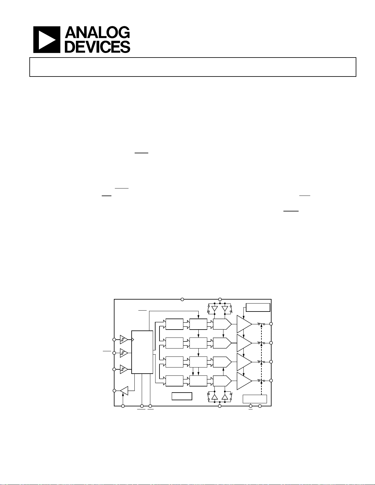
FUNCTIONAL BLOCK DIAGRAM
AD5307/AD5317/AD5327
LDAC
8-/10-/12-Bit DACs in 16-Lead TSSOP
AD5307/AD5317/AD5327
GENERAL DESCRIPTION
The AD5307/AD5317/AD53271 are quad 8-,10-,12-bit buffered
voltage-output DACs in 16-lead TSSOP that operate from single
2.5 V to 5.5 V supplies and consume 400 A at 3 V. Their onchip output amplifiers allow the outputs to swing rail-to-rail with
a slew rate of 0.7 V/s. The AD5307/AD5317/AD5327 utilize
versatile 3-wire serial interfaces that operate at clock rates up to
30 MHz; these parts are compatible with standard SPI, QSPI,
MICROWIRE, and DSP interface standards.
The references for the four DACs are derived from two reference
pins (one per DAC pair). These reference inputs can be configured
as buffered or unbuffered inputs. Each part incorporates a poweron reset circuit, ensuring that the DAC outputs power up to 0 V
and remain there until a valid write to the device takes place.
CLR
LDAC
input. Each part
pin that clears all
INPUT
REGISTER
V
DD
There is also an asynchronous active low
DACs to 0 V. The outputs of all DACs can be updated simultaneously using the asynchronous
contains a power-down feature that reduces the current
consumption of the device to 300 nA @ 5 V (90 nA @ 3 V). The
parts can also be used in daisy-chaining applications using the
SDO pin.
All three parts are offered in the same pinout, allowing users to
select the amount of resolution appropriate for their application
without redesigning their circuit board.
V
AB
REF
GAIN-SELECT
LOGIC
DAC
REGISTER
STRING
DAC A
BUFFER
V
A
OUT
SCLK
SYNC
DIN
SDO
1
Protected by U.S. Patent No. 5,969,657; other patents pending.
Rev. C
Information furnished by Analog Devices is believed to be accurate and reliable. However, no
responsibility is assumed by Anal og Devices for its use, nor for any infringements of patents or ot her
rights of third parties that may result from its use. Specifications subject to change without notice. No
license is granted by implication or otherwise under any patent or patent rights of Analog Devices.
Trademarks and registered trademarks are the property of their respective owners.
INTERFACE
LOGIC
INPUT
REGISTER
INPUT
REGISTER
INPUT
REGISTER
POWER-ON
RESET
DAC
REGISTER
DAC
REGISTER
DAC
REGISTER
STRING
DAC B
STRING
DAC C
STRING
DAC D
V
REF
V
BUFFER
BUFFER
BUFFER
POWER-DOWN
LOGIC
CD
GND
PDLDAC CLRDCEN
B
OUT
V
C
OUT
V
D
OUT
02067-001
Figure 1.
One Technology Way, P.O. Box 9106, Norwood, MA 02062-9106, U.S.A.
Tel: 781.329.4700 www.analog.com
Fax: 781.461.3113 ©2006 Analog Devices, Inc. All rights reserved.

AD5307/AD5317/AD5327
TABLE OF CONTENTS
Features .............................................................................................. 1
Input Shift Register .................................................................... 17
Applications....................................................................................... 1
General Description......................................................................... 1
Functional Block Diagram .............................................................. 1
Revision History ............................................................................... 2
Specifications..................................................................................... 3
AC Characteristics........................................................................ 5
Timing Characteristics ................................................................ 5
Absolute Maximum Ratings............................................................ 7
ESD Caution.................................................................................. 7
Pin Configuration and Function Descriptions............................. 8
Typical Performance Characteristics ............................................. 9
Te r mi n ol o g y .................................................................................... 13
Transf e r Fu ncti o n ........................................................................... 14
Functional Description ..................................................................15
Digital-to-Analog Section ......................................................... 15
Resistor String............................................................................. 15
DAC Reference Inputs ............................................................... 15
Output Amplifier........................................................................ 16
Power-On Reset .......................................................................... 16
Control Bits................................................................................. 17
Low Power Serial Interface ....................................................... 18
Daisy Chaining ........................................................................... 18
Double-Buffered Interface........................................................ 18
Load DAC Input (
Power-Down Mode .................................................................... 18
Microprocessor Interfacing....................................................... 19
Applications..................................................................................... 20
Typical Applicat i o n C i rc uit ....................................................... 20
Driving V
Bipolar Operation....................................................................... 20
Opto-Isolated Interface for Process-Control Applications... 21
Decoding Multiple AD5307/AD5317/AD5327 Devices....... 21
AD5307/AD5317/AD5327 as Digitally Programmable
Window Detectors ..................................................................... 21
Daisy Chaining ........................................................................... 22
Power Supply Bypassing and Grounding................................ 22
Outline Dimensions ....................................................................... 24
Ordering Guide .......................................................................... 25
DD
LDAC
).......................................................... 18
from the Reference Voltage................................ 20
Serial Interface ................................................................................ 17
REVISION HISTORY
3/06—Rev. B to Rev. C
Changes to Table 3............................................................................ 5
Changes to Ordering Guide.......................................................... 25
10/05—Rev. A to Rev. B
Updated Format..................................................................Universal
Changes to Bipolar Operation Section ........................................ 21
Changes to Ordering Guide.......................................................... 25
Rev. C | Page 2 of 28
8/03—Rev. 0 to Rev. A
Added A Version ................................................................Universal
Changes to Features ..........................................................................1
Changes to Specifications.................................................................2
Changes to Absolute Maximum Ratings........................................6
Changes to Ordering Guide.............................................................6
Changes to TPC 21......................................................................... 12
Added Octals section to Table II.................................................. 20
Updated Outline Dimensions....................................................... 21
AD5307/AD5317/AD5327
SPECIFICATIONS
VDD = 2.5 V to 5.5 V, V
Table 1.
A Version
Parameter
DC PERFORMANCE
DAC REFERENCE INPUTS
OUTPUT CHARACTERISTICS
2
3, 4
AD5307
Resolution 8 8 Bits
Relative Accuracy ±0.15 ±1 ±0.15 ±0.625 LSB
Differential Nonlinearity ±0.02 ±0.25 ±0.02 ±0.25 LSB Guaranteed monotonic by design
AD5317
Resolution 10 10 Bits
Relative Accuracy ±0.5 ±4 ±0.5 ±2.5 LSB
Differential Nonlinearity ±0.05 ±0.5 ±0.05 ±0.5 LSB Guaranteed monotonic by design
AD5327
Resolution 12 12 Bits
Relative Accuracy ±2 ±16 ±2 ±10 LSB
Differential Nonlinearity ±0.2 ±1 ±0.2 ±1 LSB Guaranteed monotonic by design
Offset Error ±5 ±60 ±5 ±60 mV VDD = 4.5 V, gain = 2; see Figure 29
Gain Error ±0.3 ±1.25 ±0.3 ±1.25 % FSR VDD = 4.5 V, gain = 2; see Figure 29
Lower Dead Band
Upper Dead Band 10 60 10 60 mV See Figure 30, upper dead band
Offset Error Drift
6
Gain Error Drift −5 −5 ppm of
DC Power Supply Rejection Ratio −60 −60 dB ∆VDD = ±10%
DC Crosstalk 200 200 mV RL = 2 kΩ to GND or V
V
Input Range 1 V
REF
0.25 V
V
Input Impedance (R
REF
74 90 74 90 kΩ Unbuffered reference mode,
37 45 37 45 kΩ Unbuffered reference mode,
Reference Feedthrough −90 −90 dB Frequency = 10 kHz
Channel-to-Channel Isolation −75 −75 dB Frequency = 10 kHz
Minimum Output Voltage
Maximum Output Voltage V
DC Output Impedance 0.5 0.5 Ω
Short-Circuit Current 25 25 mA VDD = 5 V
16 16 mA VDD = 3 V
Power-Up Time 2.5 2.5 μs Coming out of power-down mode,
5 5 μs Coming out of power-down mode,
= 2 V, RL = 2 k to GND, CL = 200 pF to GND. All specifications T
REF
1
B Version
MIN
to T
, unless otherwise noted.
MAX
Min Typ Max Min Typ Max Unit Conditions/Comments
over all codes
over all codes
over all codes
Figure 30
and
Figure 30
5
10 60 10 60 mV See Figure 29, lower dead band
and
exists only if offset error is negative
exists only if V
plus gain error is positive
−12 −12 ppm of
FSR/°C
FSR/°C
DD
DD
) >10 >10 MΩ Buffered reference mode and
DAC
1 V
0.25 V
DD
DD
V Buffered reference mode
V Unbuffered reference mode
power-down mode
0 V to V
0 V to 2 V
7
0.001 0.001 V A measure of the minimum drive
output range
REF
REF
capability of the output amplifier
−
DD
0.001
V
−
DD
0.001
V A measure of the maximum drive
capability of the output amplifier
V
= 5 V
DD
V
= 3 V
DD
= VDD and offset
REF
DD
output range
Rev. C | Page 3 of 28

AD5307/AD5317/AD5327
A Version
Parameter
2
Min Typ Max Min Typ Max Unit Conditions/Comments
1
B Version
LOGIC INPUTS
Input Current ±1 ±1 mA
Input Low Voltage, VIL 0.8 0.8 V VDD = 5 V ± 10%
0.6 0.6 V VDD = 3 V ± 10%
0.5 0.5 V VDD = 2.5 V
Input High Voltage, VIH
(Excluding DCEN)
1.7 1.7 V VDD = 2.5 V to 5.5 V; TTL and
1.8 V CMOS compatible
Input High Voltage, VIH
2.4 2.4 VDD = 5 V ± 10%
(DCEN)
2.1 2.1 V VDD = 3 V ± 10%
2.0 2.0 V VDD = 2.5 V
Pin Capacitance 3 3 pF
LOGIC OUTPUT (SDO)
VDD = 4.5 V to 5.5 V
Output Low Voltage, VOL 0.4 0.4 V I
Output High Voltage, VOH VDD − 1 VDD − 1 V I
= 2 mA
SINK
SOURCE
= 2 mA
VDD = 2.5 V to 3.6 V
Output Low Voltage, VOL 0.4 0.4 V I
Output High Voltage, VOH VDD −
0.5
V
−
DD
0.5
V I
= 2 mA
SINK
SOURCE
= 2 mA
Floating State Leakage Current ±1 ±1 μA DCEN = GND
Floating State Output Capacitance 3 3 pF DCEN = GND
POWER REQUIREMENTS
VDD 2.5 5.5 2.5 5.5 V
IDD (Normal Mode)8 V
VDD = 4.5 V to 5.5 V 500 900 500 900 μA
VDD = 2.5 V to 3.6 V 400 750 400 750 μA
= VDD and VIL = GND
IH
All DACs in unbuffered mode; in
buffered mode, extra current is
typically x mA per DAC, where
x = 5 mA + V
REF/RDAC
IDD (Power-Down Mode) VIH = VDD and VIL = GND
VDD = 4.5 V to 5.5 V 0.3 1 0.3 1 μA
VDD = 2.5 V to 3.6 V 0.09 1 0.09 1 μA
1
Temperature range (A, B versions): −40°C to +105°C; typical at +25°C.
2
See the Terminology section.
3
DC specifications tested with the outputs unloaded, unless otherwise noted.
4
Linearity is tested using a reduced code range: AD5307 (Code 8 to Code 255); AD5317 (Code 28 to Code 1023); AD5327 (Code 115 to Code 4095).
5
This corresponds to x codes, where x = deadband voltage/LSB size.
6
Guaranteed by design and characterization; not production tested.
7
For the amplifier output to reach its minimum voltage, offset error must be negative. For the amplifier output to reach its maximum voltage, V
gain error must be positive.
8
Interface inactive. All DACs active. DAC outputs unloaded.
= VDD and offset plus
REF
Rev. C | Page 4 of 28
AD5307/AD5317/AD5327
AC CHARACTERISTICS
VDD = 2.5 V to 5.5 V, RL = 2 k to GND, CL = 200 pF to GND. All specifications T
Table 2.
A, B Versions
Parameter
2, 3
Min Typ Max Unit Conditions/Comments
1
Output Voltage Settling Time V
AD5307 6 8 μs 1/4 scale to 3/4 scale change (0x40 to 0xC0)
AD5317 7 9 μs 1/4 scale to 3/4 scale change (0x100 to 0x300)
AD5327 8 10 μs 1/4 scale to 3/4 scale change (0x400 to 0xC00)
Slew Rate 0.7 V/μs
Major-Code Change Glitch Energy 12 nV-s 1 LSB change around major carry
Digital Feedthrough 0.5 nV-s
SDO Feedthrough 4 nV-s Daisy-chain mode; SDO load is 10 pF
Digital Crosstalk 0.5 nV-s
Analog Crosstalk 1 nV-s
DAC-to-DAC Crosstalk 3 nV-s
Multiplying Bandwidth 200 kHz V
Total Harmonic Distortion −70 dB V
1
Temperature range (A, B versions): −40°C to +105°C; typical at +25°C.
2
Guaranteed by design and characterization; not production tested.
3
See the Terminology section.
to T
MIN
= VDD = 5 V
REF
= 2 V ± 0.1 V p-p; unbuffered mode
REF
= 2.5 V ± 0.1 V p-p; frequency = 10 kHz
REF
, unless otherwise noted.
MAX
TIMING CHARACTERISTICS
VDD = 2.5 V to 5.5 V; all specifications T
Table 3.
A, B Versions
Parameter
3
1, , 2
Limit at T
MIN
, T
MAX
t1 33 ns min SCLK cycle time
t2 13 ns min SCLK high time
t3 13 ns min SCLK low time
t4 13 ns min
t5 5 ns min Data set-up time
t6 4.5 ns min Data hold time
t7 5 ns min
t8 50 ns min
t9 20 ns min
t10 20 ns min
t11 20 ns min
t12 0 ns min
4, 5
t
13
20 ns max SCLK rising edge to SDO valid (VDD = 3.6 V to 5.5 V)
25 ns max SCLK rising edge to SDO valid (VDD = 2.5 V to 3.5 V)
t
14
t
15
t
16
1
Guaranteed by design and characterization; not production tested.
2
All input signals are specified with tR = tF = 5 ns (10% to 90% of VDD) and timed from a voltage level of (VIL + VIH)/2.
3
See Figure 3 and Figure 4.
4
This is measured with the load circuit of Figure 2. t13 determines maximum SCLK frequency in daisy-chain mode.
5
Daisy-chain mode only.
5 ns min
8 ns min
0 ns min
MIN
to T
, unless otherwise noted.
MAX
Unit Conditions/Comments
SYNC to SCLK falling edge set-up time
SCLK falling edge to
Minimum
SYNC high time
SYNC rising edge
LDAC pulse width
SCLK falling edge to
LDAC rising edge
CLR pulse width
SCLK falling edge to
SCLK falling edge to
LDAC falling edge
SYNC rising edge
SYNC rising edge to SCLK rising edge
SYNC rising edge to LDAC falling edge
Rev. C | Page 5 of 28
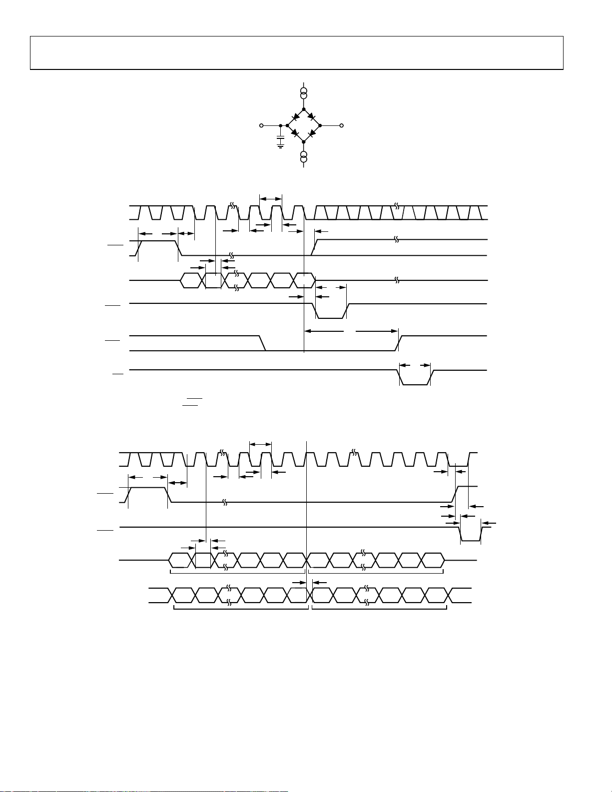
AD5307/AD5317/AD5327
2mA I
OL
SCLK
t
t
8
SYNC
DIN
1
LDAC
2
LDAC
CLR
NOTES
1
ASYNCHRONOUS LDAC UPDATE MODE.
2
SYNCHRONOUS LDAC UPDATE MODE.
DB15
TO OUTPUT
PIN
50pF
C
L
2mA I
OH
V
OH (MIN)
02067-002
Figure 2. Load Circuit for Digital Output (SDO) Timing Specifications
t
1
t
4
t
5
t
3
t
6
2
DB0
t
7
t
9
t
12
t
10
Figure 3. Serial Interface Timing Diagram
t
11
02067-003
t
1
SCLK
t
14
t
15
t
16
DB0
t
9
02067-004
SYNC
LDAC
DIN
SDO
t
t
t
8
4
t
DB15
INPUT WORD FOR DAC N INPUT WORD FOR DAC (N+1)
t
3
t
6
5
UNDEFINED INPUT WORD FOR DAC N
2
DB0 DB15' DB0'
t
13
DB15
Figure 4. Daisy-Chaining Timing Diagram
Rev. C | Page 6 of 28
AD5307/AD5317/AD5327
ABSOLUTE MAXIMUM RATINGS
TA = 25°C, unless otherwise noted.
Table 4.
Parameter
VDD to GND −0.3 V to +7 V
Digital Input Voltage to GND −0.3 V to VDD + 0.3 V
Digital Output Voltage to GND −0.3 V to VDD + 0.3 V
Reference Input Voltage to GND −0.3 V to VDD + 0.3 V
V
OUT
Operating Temperature Range
Industrial (A, B Versions) −40°C to +105°C
Storage Temperature Range −65°C to +150°C
Junction Temperature (TJ max) 150°C
16-Lead TSSOP
Power Dissipation (TJ max − TA)/θ
θJA Thermal Impedance 150.4°C/W
Reflow Soldering
Peak Temperature 220°C
Time at Peak Temperature 10 sec to 40 sec
1
Transient currents of up to 100 mA do not cause SCR latch-up.
1
A − V
D to GND −0.3 V to VDD + 0.3 V
OUT
Ratings
JA
Stresses above those listed under Absolute Maximum Ratings
may cause permanent damage to the device. This is a stress
rating only; functional operation of the device at these or any
other conditions above those indicated in the operational
section of this specification is not implied. Exposure to absolute
maximum rating conditions for extended periods may affect
device reliability.
ESD CAUTION
ESD (electrostatic discharge) sensitive device. Electrostatic charges as high as 4000 V readily accumulate on
the human body and test equipment and can discharge without detection. Although this product features
proprietary ESD protection circuitry, permanent damage may occur on devices subjected to high energy
electrostatic discharges. Therefore, proper ESD precautions are recommended to avoid performance
degradation or loss of functionality.
Rev. C | Page 7 of 28
AD5307/AD5317/AD5327
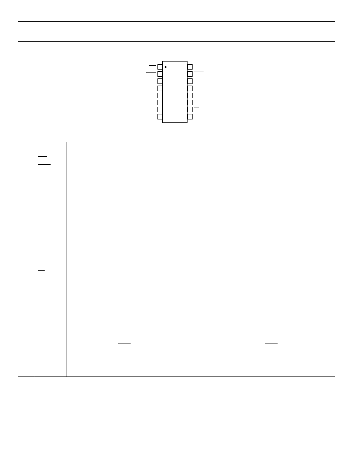
PIN CONFIGURATION AND FUNCTION DESCRIPTIONS
V
V
LDAC
V
OUT
V
OUT
V
OUT
REF
REF
CLR
V
DD
AB
CD
1
2
3
4
A
5
B
6
C
7
8
AD5307/
AD5317/
AD5327
TOP VIEW
(Not to Scale)
16
SDO
SYNC
15
SCLK
14
13
DIN
12
GND
11
V
D
OUT
10
PD
DCEN
9
02067-005
Figure 5. Pin Configuration
Table 5. Pin Function Descriptions
Pin
No.
Mnemonic Description
1
CLR
2
LDAC Active Low Control Input. Transfers the contents of the input registers to their respective DAC registers. Pulsing this
Active Low Control Input. Loads all 0s to all input and DAC registers. Therefore, the outputs also go to 0 V.
pin low allows any or all DAC registers to be updated if the input registers have new data. This allows simultaneous
update of all DAC outputs. Alternatively, this pin can be tied permanently low.
3 VDD
Power Supply Input. These parts can be operated from 2.5 V to 5.5 V, and the supply should be decoupled with a 10 μF
capacitor in parallel with a 0.1 μF capacitor to GND.
4 V
5 V
6 V
7 V
A Buffered Analog Output Voltage from DAC A. The output amplifier has rail-to-rail operation.
OUT
B Buffered Analog Output Voltage from DAC B. The output amplifier has rail-to-rail operation.
OUT
C Buffered Analog Output Voltage from DAC C. The output amplifier has rail-to-rail operation.
OUT
REF
AB
Reference Input Pin for DAC A and DAC B. It can be configured as a buffered or unbuffered input to each or both of
the DACs, depending on the state of the BUF bits in the serial input words to DAC A and DAC B. It has an input range
in unbuffered mode and 1 V to VDD in buffered mode.
DD
8 V
REF
CD
of 0.25 V to V
Reference Input Pin for DAC C and DAC D. It can be configured as a buffered or unbuffered input to each or both of
the DACs, depending on the state of the BUF bits in the serial input words to DAC C and DAC D. It has an input range
in unbuffered mode and 1 V to VDD in buffered mode.
DD
9 DCEN
of 0.25 V to V
Enables the Daisy-Chaining Option. It should be tied high if the part is being used in a daisy chain, and tied low if it is
being used in standalone mode.
10
PD Active Low Control Input. It acts like a hardware power-down option. All DACs go into power-down mode when this
pin is tied low. The DAC outputs go into a high impedance state, and the current consumption of the part drops to
300 nA @ 5 V (90 nA @ 3 V).
11 V
D Buffered Analog Output Voltage from DAC D. The output amplifier has rail-to-rail operation.
OUT
12 GND Ground Reference Point for All Circuitry on the Part.
13 DIN
Serial Data Input. These devices each have a 16-bit shift register. Data is clocked into the register on the falling edge of
the serial clock input. The DIN input buffer is powered down after each write cycle.
14 SCLK
Serial Clock Input. Data is clocked into the input shift register on the falling edge of the serial clock input. Data can be
transferred at rates of up to 30 MHz. The SCLK input buffer is powered down after each write cycle.
15
SYNC Active Low Control Input. This is the frame synchronization signal for the input data. When SYNC goes low, it powers
on the SCLK and DIN buffers and enables the input shift register. Data is transferred in on the falling edges of the
following 16 clocks. If SYNC is taken high before the 16th falling edge, the rising edge of SYNC acts as an interrupt and
the write sequence is ignored by the device.
16 SDO
Serial Data Output. Can be used for daisy-chaining a number of these devices together or for reading back the data in
the shift register for diagnostic purposes. The serial data is transferred on the rising edge of SCLK and is valid on the
falling edge of the clock.
Rev. C | Page 8 of 28
AD5307/AD5317/AD5327
TYPICAL PERFORMANCE CHARACTERISTICS
1.0
0.5
TA = 25°C
V
= 5V
DD
0.3
0.2
0.1
TA = 25°C
V
= 5V
DD
0
INL ERROR (LSB)
–0.5
–1.0
0 50 100 150 200
CODE
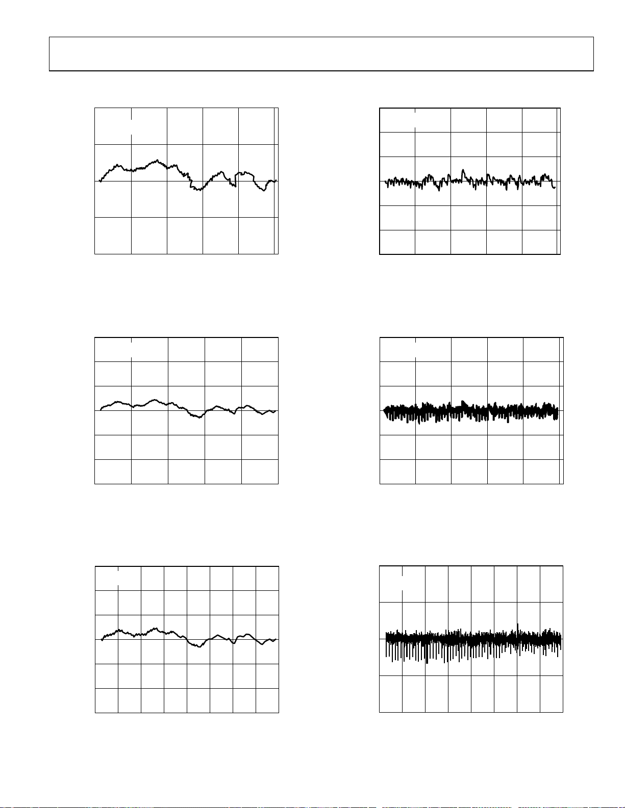
Figure 6. AD5307 INL
3
2
1
0
INL ERROR (LSB)
–1
–2
TA = 25°C
V
= 5V
DD
250
02067-006
0
–0.1
DNL ERROR (LSB)
–0.2
–0.3
0 50 100 150 200
CODE
Figure 9. AD5307 DNL
0.6
TA = 25°C
V
= 5V
0.4
0.2
–0.2
DNL ERROR (LSB)
–0.4
DD
0
02067-009
250
–3
0 200 400 600 900
CODE
Figure 7. AD5317 INL
12
TA = 25°C
V
= 5V
DD
8
4
0
INL ERROR (LSB)
–4
–8
–12
0 1000 2000 3000
CODE
Figure 8. AD5327 INL
02067-007
1000
02067-008
4000
Rev. C | Page 9 of 28
–0.6
0 200 400 600 800
CODE
Figure 10. AD5317 DNL
1.0
TA = 25°C
= 5V
V
DD
0.5
0
DNL ERROR (LSB)
–0.5
–1.0
0 1000 2000 3000
CODE
Figure 11. AD5327 DNL
02067-010
1000
02067-011
4000

AD5307/AD5317/AD5327
0.50
TA = 25°C
= 5V
V
DD
0.25
MAX INL
MAX DNL
0.2
0.1
–0.1
TA = 25°C
= 2V
V
REF
0
GAIN ERROR
0
ERROR (LSB)
REF
MIN INL
MIN INL
45
(V)
–0.25
–0.50
0123
V
Figure 12. AD5307 INL Error and DNL Error vs. V
0.5
VDD = 5V
0.4
0.3
0.2
0.1
0
–0.1
ERROR (LSB)
–0.2
–0.3
–0.4
–0.5
–40 0 40 80
= 3V
V
REF
MAX INL
MAX DNL
MIN DNL
MIN INL
TEMPERATURE (°C)
Figure 13. AD5307 INL Error and DNL Error vs. Temperature
–0.2
–0.3
ERROR (% FSR)
V
DD
(V)
5V SINK
OFFSET ERROR
02067-015
6
DD
3V SINK
02067-016
6
–0.4
–0.5
02067-012
–0.6
012345
REF
(V)
OUT
V
02067-013
120
Figure 15. Offset Error and Gain Error vs. V
5
4
3
2
1
0
012345
Figure 16. V
5V SOURCE
3V SOURCE
SINK/SOURCE CURRENT (mA)
Source and Sink Current Capability
OUT
1.0
VDD = 5V
V
= 2V
REF
0.5
GAIN ERROR
0
ERROR (% FSR)
–0.5
–1.0
–40 0 40 80
OFFSET ERROR
TEMPERATURE (°C)
Figure 14. AD5307 Offset Error and Gain Error vs. Temperature
02067-014
120
Rev. C | Page 10 of 28
600
500
400
(µA)
300
DD
I
200
100
0
ZERO SCALE
CODE
Figure 17. Supply Current vs. DAC Code
TA = 25°C
V
= 5V
DD
V
= 2V
REF
FULL SCALE
02067-017

AD5307/AD5317/AD5327
600
+25°C
500
400
(µA)
300
DD
I
200
100
0
2.5 3.0 3.5 4.0 4. 5 5.0 5.5
+105°C
V
DD
Figure 18. Supply Current vs. Supply Voltage
0.5
(V)
–40°C
TA = 25°C
= 5V
V
DD
= 5V
V
REF
CH1
V
A
OUT
SCLK
CH2
02067-018
CH1 1V, CH2 5V, T IME BASE = 1µs/DIV
02067-021
Figure 21. Half-Scale Settling (1/4 to 3/4 Scale Code Change)
0.4
0.3
(µA)
DD
I
0.2
0.1
0
2.5 3.0 3.5 4.0 4. 5 5.0 5.5
V
+25°C
DD
–40°C
+105°C
(V)
Figure 19. Power-Down Current vs. Supply Voltage
800
700
600
(µA)
DD
I
500
DECREASING
INCREASING
VDD = 5V
TA = 25°C
TA = 25°C
= 5V
V
DD
= 2V
V
CH1
CH2
02067-019
REF
V
DD
V
A
OUT
CH1 2.00V, CH2 200mV, TIME BAS E = 200µs/DI V
02067-022
Figure 22. Power-On Reset to 0 V
TA = 25°C
V
= 5V
DD
V
= 2V
CH1
REF
V
A
OUT
400
300
01 2 34 5
INCREASING
DECREASING
V
LOGIC
VDD = 3V
02067-020
(V)
Figure 20. Supply Current vs. Logic Input Voltage for SCLK and DIN Increasing
and Decreasing
Rev. C | Page 11 of 28
CH2
PD
CH1 500MV, CH2 5.00V , TIME BASE = 1µs/DI V
Figure 23. Exiting Power-Down to Midscale
02067-023

AD5307/AD5317/AD5327
VDD = 3V
FREQUENCY
VDD = 5V
FULL-SCALE ERROR (V)
0.02
0.01
–0.01
VDD= 5V
T
= 25°C
A
0
350 400 450 500 550 600
2.50
2.49
(V)
OUT
V
2.48
2.47
Figure 24. I
Histogram with VDD = 3 V and VDD = 5 V
DD
I
DD
1µs/DIV
(µA)
Figure 25. AD5327 Major-Code Transition Glitch Energy
02067-024
02067-025
–0.02
012345
Figure 27. Full-Scale Error vs. V
1mV/DIV
V
REF
150ns/DIV
(V)
REF
02067-027
6
02067-028
Figure 28. DAC-to-DAC Crosstalk
10
0
–10
–20
(dB)
–30
–40
–50
–60
10 100 1k 10k 100k 1M
FREQUENCY (Hz)
10M
Figure 26. Multiplying Bandwidth (Small-Signal Frequency Response)
02067-026
Rev. C | Page 12 of 28

AD5307/AD5317/AD5327
TERMINOLOGY
Relative Accuracy
For the DAC, relative accuracy, or integral nonlinearity (INL), is
a measure of the maximum deviation in LSB from a straight line
passing through the endpoints of the DAC transfer function.
Figure 6 through Figure 8 show plots of typical INL vs. code.
Differential Nonlinearity
Differential nonlinearity (DNL) is the difference between the
measured change and the ideal 1 LSB change between any two
adjacent codes. A specified differential nonlinearity of ±1 LSB
maximum ensures monotonicity. This DAC is guaranteed
monotonic by design.
typical DNL vs. code.
Offset Error
Offset error is a measure of the deviation in the output voltage
from 0 V when zero-code is loaded to the DAC (see
and
Figure 30.) It can be negative or positive. It is expressed in
millivolts.
Gain Error
Gain error is a measure of the span error of the DAC. It is the
deviation in slope of the actual DAC transfer characteristic from
the ideal expressed as a percentage of the full-scale range.
Offset Error Drift
Offset error drift is a measure of the change in offset error
with changes in temperature. It is expressed in (ppm of fullscale range)/°C.
Gain Error Drift
Gain error drift is a measure of the change in gain error
with changes in temperature. It is expressed in (ppm of fullscale range)/°C.
DC Power Supply Rejection Ratio (PSRR)
PSRR indicates how the output of the DAC is affected by
changes in the supply voltage. It is the ratio of the change in
V
to a change in VDD for full-scale output of the DAC. It is
OUT
measured in decibels. V
Figure 9 through Figure 11 show plots of
Figure 29
is held at 2 V, and VDD is varied ±10%.
REF
Major-Code Transition Glitch Energy
Major-code transition glitch energy is the energy of the impulse
injected into the analog output when the code in the DAC
register changes state. It is normally specified as the area of the
glitch in nV-s and is measured when the digital code is changed
by 1 LSB at the major carry transition (011 . . . 11 to 100 . . . 00
or 100 . . . 00 to 011 . . . 11).
Digital Feedthrough
Digital feedthrough is a measure of the impulse injected into
the analog output of a DAC from the digital input pins of the
device, but it is measured when the DAC is not being written to
SYNC
(
held high). It is specified in nV-s and is measured with a
full-scale change on the digital input pins, that is, from all 0s to
all 1s or vice versa.
Digital Crosstalk
Digital crosstalk is the glitch impulse transferred to the output
of one DAC at midscale in response to a full-scale code change
(all 0s to all 1s or vice versa) in the input register of another DAC.
It is measured in standalone mode and is expressed in nV-s.
Analog Crosstalk
Analog crosstalk is the glitch impulse transferred to the output
of one DAC due to a change in the output of another DAC. It is
measured by loading one of the input registers with a full-scale
code change (all 0s to all 1s or vice versa) while keeping
high, and then pulsing
the DAC whose digital code has not changed. The area of the
glitch is expressed in nV-s.
DAC-to-DAC C rosst a l k
DAC-to-DAC crosstalk is the glitch impulse transferred to the
output of one DAC due to a digital code change and subsequent
output change of another DAC. This includes both digital and
analog crosstalk. It is measured by loading one of the DACs
with a full-scale code change (all 0s to all 1s or vice versa) with
LDAC
low while monitoring the output of another DAC. The
energy of the glitch is expressed in nV-s.
LDAC
low and monitoring the output of
LDAC
DC Crosstalk
DC crosstalk is the dc change in the output level of one DAC in
response to a change in the output of another DAC. It is measured
with a full-scale output change on one DAC while monitoring
another DAC. It is expressed in microvolts.
Reference Feedthrough
Reference feedthrough is the ratio of the amplitude of the signal at
the DAC output to the reference input when the DAC output is not
being updated (that is,
Channel-to-Channel Isolation
Channel-to-channel isolation is the ratio of the amplitude of the
signal at the output of one DAC to a sine wave on the reference
input of another DAC. It is measured in decibels.
LDAC
is high). It is expressed in decibels.
Rev. C | Page 13 of 28
Multiplying Bandwidth
The amplifiers within the DAC have a finite bandwidth, and the
multiplying bandwidth is a measure of this. A sine wave on the
reference (with full-scale code loaded to the DAC) appears on
the output. The multiplying bandwidth is the frequency at
which the output amplitude falls to 3 dB below the input.
Total Harmonic Distortion (THD)
THD is the difference between an ideal sine wave and its attenuated
version using the DAC. The sine wave is used as the reference for
the DAC, and the THD is a measure of the harmonics present
on the DAC output. It is measured in decibels.

AD5307/AD5317/AD5327
R
V
TRANSFER FUNCTION
OUTPUT
VOLTAGE
NEGATI VE
OFFSET
ERROR
AMPLIFIER
FOOTROOM
ER
W
LO
DEAD BAND
DES
CO
DAC CODE
ACTUAL
IDEAL
GAIN ERROR
+
OFFSET ERRO
NEGATIVE
OFFSET
ERROR
02067-029
Figure 29. Transfer Function with Negative Offset
GAIN ERROR
+
OFFSET ERROR
UPPER
OUTPUT
OLTAGE
POSITIVE
OFFSET
ERROR
DAC CODE
Figure 30. Transfer Function with Positive Offset (V
DEADBAND
CODES
ACTUAL
IDEAL
FULL SCALE
REF
= VDD)
02067-030
Rev. C | Page 14 of 28

AD5307/AD5317/AD5327
FUNCTIONAL DESCRIPTION
The AD5307/AD5317/AD5327 are quad resistor-string DACs
fabricated on a CMOS process with resolutions of 8, 10, and 12
bits respectively. Each contains four output buffer amplifiers
and is written to via a 3-wire serial interface. They operate from
single supplies of 2.5 V to 5.5 V, and the output buffer amplifiers
provide rail-to-rail output swing with a slew rate of 0.7 V/µs.
DAC A and DAC B share a common reference input, V
DAC C and DAC D share a common reference input, V
REF
REF
AB.
CD.
Each reference input can be buffered to draw virtually no
current from the reference source, or can be unbuffered to give
a reference input range of 0.25 V to V
. The devices have a
DD
power-down mode in which all DACs can be completely turned
off with a high impedance output.
DIGITAL-TO-ANALOG SECTION
The architecture of one DAC channel consists of a resistorstring DAC followed by an output buffer amplifier. The voltage
at the V
corresponding DAC.
DAC architecture. Because the input coding to the DAC is
straight binary, the ideal output voltage is given by
where:
D is the decimal equivalent of the binary code that is loaded to
the DAC register:
0 to 255 for AD5307 (8 bits).
0 to 1023 for AD5317 (10 bits).
0 to 4095 for AD5327 (12 bits).
N is the DAC resolution.
REGISTER
pin provides the reference voltage for the
REF
Figure 31 shows a block diagram of the
DV
×
OUT
REF
=
N
2
BUF
REGISTER
DAC
V
AB
REF
RESISTOR
STRING
V
INPUT
REFERENCE
BUFFER
GAIN MODE
(GAIN = 1 OR 2)
V
OUT
A
RESISTOR STRING
The resistor string section is shown in Figure 32. It is simply a
string of resistors, each of value R. The digital code loaded to
the DAC register determines at which node on the string the
voltage is tapped off to be fed into the output amplifier. The
voltage is tapped off by closing one of the switches connecting
the string to the amplifier. Because it is a string of resistors, it is
guaranteed monotonic.
DAC REFERENCE INPUTS
There is a reference pin for each pair of DACs. The reference
inputs are buffered but can also be individually configured as
unbuffered. The advantage with the buffered input is the high
impedance it presents to the voltage source driving it. However,
if the unbuffered mode is used, the user can have a reference
voltage as low as 0.25 V and as high as V
restriction due to headroom and footroom of the reference
amplifier.
R
R
R
R
R
Figure 32. Resistor String
If there is a buffered reference in the circuit (for example, REF192),
there is no need to use the on-chip buffers of the AD5307/AD5317/
AD5327. In unbuffered mode, the input impedance is still large
at typically 90 k per reference input for 0 V to V
45 k or 0 V to 2 V
mode.
REF
The buffered/unbuffered option is controlled by the BUF bit in
the data-word. The BUF bit setting applies to whichever DAC is
selected.
, because there is no
DD
TO OUTPUT
AMPLIFIER
02067-032
mode and
REF
OUTPUT
BUFFER AMPLIFIER
Figure 31. Single DAC Channel Architecture
02067-031
Rev. C | Page 15 of 28

AD5307/AD5317/AD5327
OUTPUT AMPLIFIER
The output buffer amplifier is capable of generating output
voltages to within 1 mV of either rail. Its actual range depends
on the value of V
, GAIN, offset error, and gain error.
REF
POWER-ON RESET
The AD5307/AD5317/AD5327 are each provided with a poweron reset function so that they power up in a defined state. The
power-on state is
If a gain of 1 is selected (GAIN = 0), the output range is 0.001 V
to V
.
REF
If a gain of 2 is selected (GAIN = 1), the output range is 0.001 V
to 2 V
is limited to V
. Because of clamping, however, the maximum output
REF
− 0.001 V.
DD
The output amplifier is capable of driving a load of 2 k to GND
or V
in parallel with 500 pF to GND or VDD. The source and
DD
sink capabilities of the output amplifier can be seen in
Figure 16.
The slew rate is 0.7 V/s, with a half-scale settling time to
±0.5 LSB (at eight bits) of 6 s.
• Normal operation
• Reference inputs unbuffered
• 0 V to V
output range
REF
• Output voltage set to 0 V
Both input and DAC registers are filled with 0s until a valid
write sequence is made to the device. This is particularly useful
in applications where it is important to know the state of the
DAC outputs while the device is powering up.
Rev. C | Page 16 of 28

AD5307/AD5317/AD5327
SERIAL INTERFACE
The AD5307/AD5317/AD5327 are controlled over versatile 3-wire
serial interfaces that operate at clock rates of up to 30 MHz and
are compatible with SPI, QSPI, MICROWIRE, and DSP
interface standards.
INPUT SHIFT REGISTER
The input shift register is 16 bits wide. Data is loaded into the
device as a 16-bit word under the control of a serial clock input,
SCLK. The timing diagram for this operation is shown in
Figure 3. The 16-bit word consists of four control bits followed
by 8, 10, or 12 bits of DAC data, depending on the device type.
Data is loaded MSB first (Bit 15), and the first two bits
determine whether the data is for DAC A, DAC B, DAC C, or
DAC D. Bit 13 and Bit 12 control the operating mode of the
DAC. Bit 13 is GAIN, which determines the output range of the
part. Bit 12 is BUF, which controls whether the reference inputs
are buffered or unbuffered.
Table 6. Address Bits for the AD53x7
A1 (Bit 15) A0 (Bit 14) DAC Addressed
0 0 DAC A
0 1 DAC B
1 0 DAC C
1 1 DAC D
CONTROL BITS
GAIN controls the output range of the addressed DAC.
0: output range of 0 V to V
1: output range of 0 V to 2 V
BUF controls whether reference of the addressed DAC is
buffered or unbuffered.
0: unbuffered reference.
1: buffered reference.
.
REF
.
REF
BIT 15
(MSB)
A1 BUF D7 D6 D5 D4 D3 D2 D1 D0GAINA0 XXXX
Figure 33. AD5307 Input Shift Register Contents
BIT 15
(MSB)
A1 BUF D9 D8 D7 D6 D5 D4 D3 D2GAINA0 D1 D0 X X
Figure 34. AD5317 Input Shift Register Contents
DATA BITS
The AD5327 uses all 12 bits of DAC data; the AD5317 uses
10 bits and ignores the 2 LSBs. The AD5307 uses eight bits and
ignores the last four bits. The data format is straight binary, with
all 0s corresponding to 0 V output and all 1s corresponding to
full-scale output (V
SYNC
The
input is a level-triggered input that acts as a frame
− 1 LSB).
REF
synchronization signal and chip enable. Data can be transferred
into the device only while
transfer,
SYNC
SYNC
should be taken low, observing the minimum
to SCLK falling edge set-up time, t4. After
SYNC
is low. To start the serial data
SYNC
low, serial data is shifted into the device’s input shift register on
the falling edges of SCLK for 16 clock pulses. In standalone
mode (DCEN = 0), any data and clock pulses after the 16th
falling edge of SCLK are ignored, and no further serial data
transfer can occur until
SYNC
can be taken high after the falling edge of the 16th SCLK
SYNC
is taken high and low again.
pulse, observing the minimum SCLK falling edge to
rising edge time, t
.
7
After the end of serial data transfer, data is automatically transferred from the input shift register to the input register of the
selected DAC. If
SYNC
is taken high before the 16th falling
edge of SCLK, the data transfer is aborted and the DAC input
registers are not updated.
When data has been transferred into the input register of a DAC,
the corresponding DAC register and DAC output can be updated
by taking
LDAC
low.
CLR
is an active low, asynchronous clear
that clears the input registers and DAC registers to all 0s.
BIT 0
(LSB)
02067-033
BIT 0
(LSB)
DATA BITS
02067-034
goes
SYNC
BIT 15
(MSB)
A1 BUF D11 D10 D9 D8 D7 D6 D5 D4GAINA0 D3 D2 D1 D0
DATA BITS
Figure 35. AD5327 Input Shift Register Contents
Rev. C | Page 17 of 28
BIT 0
(LSB)
02067-035

AD5307/AD5317/AD5327
LOW POWER SERIAL INTERFACE
To minimize the power consumption of the device, the interface
powers up fully only when the device is being written to, that is,
on the falling edge of
are powered down on the rising edge of
DAISY CHAINING
For systems that contain several DACs, or where the user
wishes to read back the DAC contents for diagnostic purposes,
the SDO pin can be used to daisy-chain several devices together
and provide serial readback.
By connecting the DCEN (daisy-chain enable) pin high, the
daisy-chain mode is enabled. It is tied low in the case of
standalone mode. In daisy-chain mode, the internal gating on
SCLK is disabled. The SCLK is continuously applied to the
input shift register when
pulses are applied, the data ripples out of the shift register and
appears on the SDO line. This data is clocked out on the rising
edge of SCLK and is valid on the falling edge. By connecting
this line to the DIN input on the next DAC in the chain, a
multi-DAC interface is constructed. Each DAC in the system
requires 16 clock pulses; therefore, the total number of clock
cycles must equal 16N, where N is the total number of devices
in the chain. When the serial transfer to all devices is complete,
SYNC
should be taken high. This prevents any further data
from being clocked into the input shift register.
A continuous SCLK source can be used if
the correct number of clock cycles. Alternatively, a burst clock
containing the exact number of clock cycles can be used and
SYNC
can be taken high some time later.
When the transfer to all input registers is complete, a common
LDAC
signal updates all DAC registers and all analog outputs
are updated simultaneously.
DOUBLE-BUFFERED INTERFACE
The AD5307/AD5317/AD5327 DACs have double-buffered
interfaces consisting of two banks of registers: input registers
and DAC registers. The input registers are connected directly to
the input shift register and the digital code is transferred to the
relevant input register on completion of a valid write sequence.
The DAC registers contain the digital code used by the resistor
strings.
Access to the DAC registers is controlled by the
When the
the input registers can change state without affecting the
contents of the DAC registers. When
however, the DAC registers become transparent and the
contents of the input registers are transferred to them.
LDAC
SYNC
. The SCLK and DIN input buffers
SYNC
.
SYNC
is low. If more than 16 clock
SYNC
is held low for
LDAC
pin.
pin is high, the DAC registers are latched and
LDAC
is brought low,
Rev. C | Page 18 of 28
The double-buffered interface is useful if the user requires
simultaneous updating of all DAC outputs. The user can write
to three of the input registers individually and then, by bringing
LDAC
low when writing to the remaining DAC input register,
all outputs update simultaneously.
These parts each contain an extra feature whereby a DAC
register is not updated unless its input register has been updated
since the last time
is brought low, the DAC registers are filled with the contents of
the input registers. In the case of the AD5307/AD5317/AD5327,
the DAC register updates only if the input register has changed
since the last time the DAC register was updated, thereby removing
unnecessary digital crosstalk.
LDAC
was brought low. Normally, when
LDAC
LOAD DAC INPUT (LDAC)
LDAC
transfers data from the input registers to the DAC
registers and therefore updates the outputs. Use of the
function enables double buffering of the DAC data, GAIN, and
BUF. There are two
LDAC
modes: synchronous and asynchronous.
LDAC
Synchronous Mode
In this mode, the DAC registers are updated after new data is
LDAC
read from on the falling edge of the 16th SCLK pulse.
can be tied permanently low or pulsed as in
Figure 3.
Asynchronous Mode
In this mode, the outputs are not updated at the same time that
the input registers are written to. When
registers are updated with the contents of the input register.
LDAC
goes low, the DAC
POWER-DOWN MODE
The AD5307/AD5317/AD5327 have low power consumption,
typically dissipating 1.2 mW with a 3 V supply and 2.5 mW with
a 5 V supply. Power consumption can be further reduced when
the DACs are not in use by putting them into power-down mode,
which is selected by taking the
When the
power consumption of 500 A at 5 V (400 A at 3 V). However,
in power-down mode, the supply current falls to 300 nA at 5 V
(90 nA at 3 V) when all DACs are powered down. Not only does
the supply current drop, but the output stage is also internally
switched from the output of the amplifier, making it an open
circuit. This has the advantage that the output is three-state
while the part is in power-down mode and provides a defined
input condition for whatever is connected to the output of the
DAC amplifier. The output stage is illustrated in
The bias generator, output amplifiers, resistor string, and all
other associated linear circuitry are shut down when the powerdown mode is activated. However, the contents of the registers
are unaffected when in power-down. In fact, it is possible to
load new data to the input registers and DAC registers during
power-down. The DAC outputs update as soon as
PD
pin is high, all DACs work normally with a typical
PD
pin low.
Figure 36.
PD
goes high.

AD5307/AD5317/AD5327
The time to exit power-down is typically 2.5 s for VDD = 5 V
and 5 s when V
PD
of
to when the output voltage deviates from its power-down
voltage. See
RESISTOR
STRING DAC
= 3 V. This is the time from the rising edge
DD
Figure 23 for a plot.
AMPLIFIER
POWER-DOWN
CIRCUITRY
Figure 36. Output Stage During Power-Down
V
OUT
02067-036
MICROPROCESSOR INTERFACING
ADSP-2101/ADSP-2103-toAD5307/AD5317/AD5327 Interface
Figure 37 shows a serial interface between the AD5307/AD5317/
AD5327 and the ADSP-2101/ADSP-2103. The ADSP-2101/
ADSP-2103 should be set up to operate in the SPORT transmit
alternate framing mode. The ADSP-2101/ADSP-2103 SPORT is
programmed through the SPORT control register and should be
configured as follows: internal clock operation, active low framing,
16-bit word length. Transmission is initiated by writing a word
to the Tx register after SPORT is enabled. The data is clocked
out on each rising edge of the DSP’s serial clock and clocked
into the AD5307/AD5317/AD5327 on the falling edge of the
DAC’s SCLK.
ADSP-2101/
ADSP-2103
1
ADDITIONAL PINS OMIT TED FOR CLARITY.
1
TFS
DT
SCLK
Figure 37. ADSP-2101/ADSP-2103-to-AD5307/AD5317/AD5327 Interface
68HC11/68L11-to-AD5307/AD5317/AD5327 Interface
Figure 38 shows a serial interface between the AD5307/AD5317/
AD5327 and the 68HC11/68L11 microcontroller. SCK of the
68HC11/68L11 drives the SCLK of the AD5307/AD5317/
AD5327, and the MOSI output drives the serial data line (DIN)
of the DAC. The
SYNC
signal is derived from a port line (PC7).
The set-up conditions for correct operation of this interface are as
follows: The 68HC11/68L11 should be configured so that its CPOL
bit is 0 and its CPHA bit is 1. When data is being transmitted to the
DAC, the
SYNC
line is taken low (PC7). With this configuration,
data appearing on the MOSI output is valid on the falling edge
of SCK. Serial data from the 68HC11/68L11 is transmitted in
8-bit bytes, with only eight falling clock edges occurring in the
transmit cycle. Data is transmitted MSB first. To load data to
the AD5307/AD5317/AD5327, PC7 is left low after the first
eight bits are transferred and a second serial write operation
is performed to the DAC. PC7 is taken high at the end of this
procedure.
AD5307/
AD5317/
AD5327
SYNC
DIN
SCLK
1
02067-037
PC7
SCK
MOSI
1
AD5307/
AD5317/
AD5327
SYNC
SCLK
DIN
1
8
3
0
7
6
0
2
0
68HC11/68L11
1
ADDITIONAL PINS OMITTED FOR CLARITY.
Figure 38. 68HC11/68L11-to-AD5307/AD5317/AD5327 Interface
80C51/80L51-to-AD5307/AD5317/AD5327 Interface
Figure 39 shows a serial interface between the AD5307/AD5317/
AD5327 and the 80C51/80L51 microcontroller. The setup for
the interface is as follows: TxD of the 80C51/80L51 drives SCLK
of the AD5307/AD5317/AD5327, and RxD drives the serial data
line of the part. The
SYNC
signal is again derived from a bitprogrammable pin on the port. In this case, Port Line P3.3 is
used. When data is to be transmitted to the AD5307/AD5317/
AD5327, P3.3 is taken low. The 80C51/80L51 transmits data only
in 8-bit bytes; therefore, only eight falling clock edges occur in
the transmit cycle. To load data to the DAC, P3.3 is left low after
the first eight bits are transmitted, and a second write cycle is
initiated to transmit the second byte of data. P3.3 is taken high
following the completion of this cycle. The 80C51/80L51 outputs
the serial data LSB first. The AD5307/AD5317/AD5327 require
their data with the MSB as the first bit received. The
80C51/80L51 transmit routine should take this into account.
80C51/80L51
1
ADDITIONAL PINS OMITTED FOR CLARITY.
1
P3.3
TxD
RxD
Figure 39. 80C51/80L51-to-AD5307/AD5317/AD5327 Interface
AD5307/
AD5317/
AD5327
SYNC
SCLK
DIN
1
02067-039
MICROWIRE-to-AD5307/AD5317/AD5327 Interface
Figure 40 shows an interface between the AD5307/AD5317/
AD5327 and a MICROWIRE-compatible device. Serial data is
shifted out on the falling edge of the serial clock, SK, and is
clocked into the AD5307/AD5317/AD5327 on the rising edge
of SK, which corresponds to the falling edge of the DAC’s SCLK.
MICROWIRE
1
ADDITIONAL PINS OMI TTED FO R CLARITY.
Figure 40. MICROWIRE-to-AD5307/AD5317/AD5327 Interface
1
CS SYNC
SK
SO
AD5307/
AD5317/
AD5327
SCLK
DIN
1
02067-040
Rev. C | Page 19 of 28

AD5307/AD5317/AD5327
V
V
(
APPLICATIONS
TYPICAL APPLICATION CIRCUIT
The AD5307/AD5317/AD5327 can be used with a wide range
of reference voltages and offer full, one-quadrant multiplying
capability over a reference range of 0.25 V to V
these devices are used with a fixed precision reference voltage.
Suitable references for 5 V operation are the AD780 and REF192
(2.5 V references). For 2.5 V operation, a suitable external reference would be the AD589, a 1.23 V band gap reference.
shows a typical setup for the AD5307/AD5317/AD5327 when
using an external reference.
= 2.5V TO 5.5
DD
1µF
SERIAL
INTERFACE
10µF
V
REF
V
REF
AD5307/AD5317/
SCLK
DIN
SYNC
V
IN
V
OUT
EXT
REF
AD780/REF192
= 5V
WITH V
DD
OR AD589 WIT H
= 2.5V
V
DD
0.1µF
Figure 41. AD5307/AD5317/AD5327 Using a 2.5 V External Reference
DRIVING VDD FROM THE REFERENCE VOLTAGE
If an output range of 0 V to VDD is required when the reference
inputs are configured as unbuffered, the simplest solution is to
connect the reference input to V
noisy and not very accurate, the AD5307/AD5317/AD5327 can
be powered from the reference voltage, for example, from a 5 V
reference such as the REF195, which outputs a steady supply
voltage. The typical current required from the REF195 with no
load on the DAC outputs is 500 A supply current and ≈112 A
into the reference inputs (if unbuffered). When the DAC
outputs are loaded, the REF195 also needs to supply the current
to the loads. The total current required with a 10 k load on
each output is
612 A + 4 (5 V/10 k) = 2.6 mA
. Because this supply can be
DD
. More typically,
DD
AB
V
CD
V
AD5327
V
OUT
V
OUT
GND
OUT
OUT
Figure 41
A
B
C
D
02067-041
BIPOLAR OPERATION
The AD5307/AD5317/AD5327 are designed for single-supply
operation, but a bipolar output range is also possible using the
circuit shown in
voltage range of 5 V. Rail-to-rail operation at the amplifier
output is achievable by using an AD820 or an OP295 as the
output amplifier.
The output voltage for any input code can be calculated as
follows:
V
OUT
where:
D is the decimal equivalent of the code loaded to the DAC.
N is the DAC resolution.
REFIN is the reference voltage input.
When REFIN = 5 V, R1 = R2 = 10 k,
V
OUT
+6V TO +16V
10µF
V
IN
REF195
V
OUT
GND
Figure 42. Bipolar Operation with the AD5307/AD5317/AD5327
Figure 42. This circuit provides an output
⎡
=
⎢
⎢
⎣
N
)
1
R
⎤
)(2/
R2R1DREFIN
+××
⎥
⎥
⎦
= (10 × D/2N) − 5 V
+5V
R1
10kΩ
1µF
0.1µF
AD5307/AD5317/
V
REF
V
REF
GND
DIN
V
V
DD
AD5327
AB
V
CD
V
V
SCLK
SYNC
SERIAL
INTERFACE
OUT
OUT
OUT
OUT
A
B
C
D
×−
R2
10kΩ
+5V
–5V
)/(
R1R2REFIN
AD820/
OP295
±5V
02067-042
The load regulation of the REF195 is typically 2 ppm/mA,
which results in an error of 5.2 ppm (26 V) for the 2.6 mA
current drawn from it. This corresponds to a 0.0013 LSB error
at eight bits and a 0.021 LSB error at 12 bits.
Rev. C | Page 20 of 28

AD5307/AD5317/AD5327
C
A
OPTO-ISOLATED INTERFACE FOR PROCESS-CONTROL APPLICATIONS
The AD5307/AD5317/AD5327 each have a versatile 3-wire serial
interface, making them ideal for generating accurate voltages in
process-control and industrial applications. Due to noise, safety
requirements, or distance, it may be necessary to isolate the
AD5307/AD5317/AD5327 from the controller. This can easily
be achieved by using opto-isolators capable of providing isolation
in excess of 3 kV. The actual data rate achieved can be limited
by the type of optocouplers chosen. The serial loading structure
of the AD5307/AD5317/AD5327 makes them ideally suited for
use in opto-isolated applications.
Figure 43 shows an opto-isolated
interface to the AD5307/AD5317/AD5327 where DIN, SCLK,
SYNC
and
are driven from optocouplers. The power supply to
the part should also be isolated. This is done by using a transformer. On the DAC side of the transformer, a 5 V regulator
provides the 5 V supply required for the AD5307/AD5317/
AD5327.
5V
POWER
SCLK
SYN
DIN
REGULATOR
V
DD
10kΩ
10kΩ
10kΩ
V
DD
V
DD
SCLK
SYNC
DIN
DCEN
V
DD
AD5307
GND
V
REF
V
REF
V
OUT
V
OUT
V
OUT
V
OUT
Figure 43. AD5307 in an Opto-Isolated Interface
10µF
AB
CD
0.1µF
A
B
C
D
02067-043
DECODING MULTIPLE AD5307/AD5317/AD5327 DEVICES
SYNC
The
applications to decode a number of DACs. In this application,
all DACs in the system receive the same serial clock and serial
data, but the
given time, allowing access to four channels in this 16-channel
system. The 74HC139 is used as a 2-to-4 line decoder to address
any of the DACs in the system. To prevent timing errors, the
enable input should be brought to its inactive state while the
coded address inputs are changing state.
diagram of a typical setup for decoding multiple AD5307
devices in a system.
pin on the AD5307/AD5317/AD5327 can be used in
SYNC
to only one of the devices is active at any
Figure 44 shows a
SCLK
DIN
ENABLE
CODED
DDRESS
1G
1A
1B
V
DD
V
CC
74HC139
DGND
1Y0
1Y1
1Y2
1Y3
Figure 44. Decoding Multiple AD5307 Devices in a System
AD5307/AD5317/AD5327 AS DIGITALLY PROGRAMMABLE WINDOW DETECTORS
A digitally programmable upper/lower limit detector using two of
the DACs in the AD5307/AD5317/AD5327 is shown in
The upper and lower limits for the test are loaded to DAC A
and DAC B, which, in turn, set the limits on the CMP04. If the
signal at the V
an LED indicates the fail condition. Similarly, DAC C and DAC D
can be used for window detection on a second V
5V
V
REF
SYNC
DIN
SCLK
input is not within the programmed window,
IN
V
REF
V
REF
SYNC
DIN
SCLK
10µF0.1µF
AB
CD
AD5307/
AD5317/
AD5327
GND
V
IN
V
DD
A
V
OUT
1/2
CMP04
V
B
OUT
Figure 45. Window Detection
AD5307
SYNC
DIN
SCLK
AD5307
SYNC
DIN
SCLK
AD5307
SYNC
DIN
SCLK
AD5307
SYNC
DIN
SCLK
V
OUT
V
OUT
V
OUT
V
OUT
V
OUT
V
OUT
V
OUT
V
OUT
V
OUT
V
OUT
V
OUT
V
OUT
V
OUT
V
OUT
V
OUT
V
OUT
signal.
IN
1kΩ
FAIL
PASS/FAIL
1/6 74HC05
A
B
C
D
A
B
C
D
A
B
C
D
A
B
C
D
Figure 45.
1kΩ
PASS
02067-044
02067-045
Rev. C | Page 21 of 28

AD5307/AD5317/AD5327
DAISY CHAINING
For systems that contain several DACs, or where the user
wishes to read back the DAC contents for diagnostic purposes,
the SDO pin can be used to daisy-chain several devices together
and provide serial readback.
for daisy-chain applications. The daisy-chain mode is enabled
by connecting DCEN high (see
1
68HC11
MOSI
SCK
PC7
PC6
MISO
1
ADDITIONAL PINS OMITTED FOR CLARITY.
Figure 46. AD5307 in Daisy-Chain Mode
Figure 4 shows the timing diagram
Figure 46).
1
AD5307
DIN
SCLK
SYNC
DCEN
LDAC
SDO
DIN
1
AD5307
SCLK
SYNC
DCEN
LDAC
SDO
DIN
1
AD5307
SCLK
SYNC
DCEN
LDAC
SDO
02067-046
POWER SUPPLY BYPASSING AND GROUNDING
In any circuit where accuracy is important, careful consideration
of the power supply and ground return layout helps to ensure
the rated performance. The printed circuit board on which the
AD5307/AD5317/AD5327 are mounted should be designed so
that the analog and digital sections are separated and confined
to certain areas of the board. If the AD5307/AD5317/AD5327
are in a system where multiple devices require an AGND-toDGND connection, the connection should be made at one
point only. The star ground point should be established as close
as possible to the device. The AD5307/AD5317/AD5327 should
have ample supply bypassing of 10 F in parallel with 0.1 F on
the supply located as close to the package as possible, ideally right
up against the device. The 10 F capacitors are the tantalum bead
type. The 0.1 F capacitor should have low effective series
resistance (ESR) and low effective series inductance (ESI), such
as is typical of the common ceramic types that provide a low
impedance path to ground at high frequencies to handle
transient currents due to internal logic switching.
The power supply lines of the AD5307/AD5317/AD5327 should
use as large a trace as possible to provide low impedance paths
and reduce the effects of glitches on the power supply line. Components, such as clocks, with fast switching signals should be
shielded with digital ground to avoid radiating noise to other
parts of the board, and they should never be run near the reference inputs. Avoid crossover of digital and analog signals. Traces
on opposite sides of the board should run at right angles to each
other. This reduces the effects of feedthrough on the board. A
microstrip technique is by far the best, but it is not always
possible with a double-sided board. In this technique, the component side of the board is dedicated to ground plane, and signal
traces are placed on the solder side.
Rev. C | Page 22 of 28

AD5307/AD5317/AD5327
Table 7. Overview of AD53xx Serial Devices
1
Part No. Resolution No. of DACs DNL Interface Settling Time (μs) Package Pin
SINGLES
AD5300 8 1 ±0.25 SPI 4 SOT-23, MSOP 6, 8
AD5310 10 1 ±0.5 SPI 6 SOT-23, MSOP 6, 8
AD5320 12 1 ±1.0 SPI 8 SOT-23, MSOP 6, 8
AD5301 8 1 ±0.25 2-Wire 6 SOT-23, MSOP 6, 8
AD5311 10 1 ±0.5 2-Wire 7 SOT-23, MSOP 6, 8
AD5321 12 1 ±1.0 2-Wire 8 SOT-23, MSOP 6, 8
DUALS
AD5302 8 2 ±0.25 SPI 6 MSOP 8
AD5312 10 2 ±0.5 SPI 7 MSOP 8
AD5322 12 2 ±1.0 SPI 8 MSOP 8
AD5303 8 2 ±0.25 SPI 6 TSSOP 16
AD5313 10 2 ±0.5 SPI 7 TSSOP 16
AD5323 12 2 ±1.0 SPI 8 TSSOP 16
QUADS
AD5304 8 4 ±0.25 SPI 6 MSOP 10
AD5314 10 4 ±0.5 SPI 7 MSOP 10
AD5324 12 4 ±1.0 SPI 8 MSOP 10
AD5305 8 4 ±0.25 2-Wire 6 MSOP 10
AD5315 10 4 ±0.5 2-Wire 7 MSOP 10
AD5325 12 4 ±1.0 2-Wire 8 MSOP 10
AD5306 8 4 ±0.25 2-Wire 6 TSSOP 16
AD5316 10 4 ±0.5 2-Wire 7 TSSOP 16
AD5326 12 4 ±1.0 2-Wire 8 TSSOP 16
AD5307 8 4 ±0.25 SPI 6 TSSOP 16
AD5317 10 4 ±0.5 SPI 7 TSSOP 16
AD5327 12 4 ±1.0 SPI 8 TSSOP 16
OCTALS
AD5308 8 8 ±0.25 SPI 6 TSSOP 16
AD5318 10 8 ±0.5 SPI 7 TSSOP 16
AD5328 12 8 ±1.0 SPI 8 TSSOP 16
1
Visit www.analog.com/support/standard_linear/selection_guides/AD53xx.html for more information.
Table 8. Overview of AD53xx Parallel Devices
Additional Pin Functions
Part No. Resolution DNL V
SINGLES
AD5330 8 ±0.25 1 6 • • • TSSOP 20
AD5331 10 ±0.5 1 7 • • TSSOP 20
AD5340 12 ±1.0 1 8 • • • TSSOP 24
AD5341 12 ±1.0 1 8 • • • • TSSOP 20
DUALS
AD5332 8 ±0.25 2 6 • TSSOP 20
AD5333 10 ±0.5 2 7 • • • TSSOP 24
AD5342 12 ±1.0 2 8 • • • TSSOP 28
AD5343 12 ±1.0 1 8 • • TSSOP 20
QUADS
AD5334 8 ±0.25 2 6 • • TSSOP 24
AD5335 10 ±0.5 2 7 • • TSSOP 24
AD5336 10 ±0.5 4 7 • • TSSOP 28
AD5344 12 ±1.0 4 8 TSSOP 28
Pin Settling Time (μs) BUF GAIN HBEN CLR Package Pin
REF
Rev. C | Page 23 of 28

AD5307/AD5317/AD5327
OUTLINE DIMENSIONS
5.10
5.00
4.90
0.15
0.05
4.50
4.40
4.30
PIN 1
16
0.65
BSC
COPLANARITY
COMPLIANT TO JEDEC STANDARDS MO-153-AB
0.10
0.30
0.19
9
BSC
81
1.20
MAX
SEATING
PLANE
6.40
0.20
0.09
8°
0°
Figure 47. 16-Lead Thin Shrink Small Outline Package [TSSOP]
(RU-16)
Dimensions shown in millimeters
0.75
0.60
0.45
Rev. C | Page 24 of 28

AD5307/AD5317/AD5327
ORDERING GUIDE
Model Temperature Range Package Description Package Option
AD5307ARU −40°C to +105°C 16-Lead Thin Shrink Small Outline Package [TSSOP] RU-16
AD5307ARU-REEL7 −40°C to +105°C 16-Lead Thin Shrink Small Outline Package [TSSOP] RU-16
AD5307ARUZ1 −40°C to +105°C 16-Lead Thin Shrink Small Outline Package [TSSOP] RU-16
AD5307ARUZ-REEL71 −40°C to +105°C 16-Lead Thin Shrink Small Outline Package [TSSOP] RU-16
AD5307BRU −40°C to +105°C 16-Lead Thin Shrink Small Outline Package [TSSOP] RU-16
AD5307BRU-REEL −40°C to +105°C 16-Lead Thin Shrink Small Outline Package [TSSOP] RU-16
AD5307BRU-REEL7 −40°C to +105°C 16-Lead Thin Shrink Small Outline Package [TSSOP] RU-16
AD5307BRUZ1 −40°C to +105°C 16-Lead Thin Shrink Small Outline Package [TSSOP] RU-16
AD5307BRUZ-REEL1 −40°C to +105°C 16-Lead Thin Shrink Small Outline Package [TSSOP] RU-16
AD5307BRUZ-REEL71 −40°C to +105°C 16-Lead Thin Shrink Small Outline Package [TSSOP] RU-16
AD5317ARU −40°C to +105°C 16-Lead Thin Shrink Small Outline Package [TSSOP] RU-16
AD5317ARU-REEL7 −40°C to +105°C 16-Lead Thin Shrink Small Outline Package [TSSOP] RU-16
AD5317ARUZ1 −40°C to +105°C 16-Lead Thin Shrink Small Outline Package [TSSOP] RU-16
AD5317BRU −40°C to +105°C 16-Lead Thin Shrink Small Outline Package [TSSOP] RU-16
AD5317BRU-REEL −40°C to +105°C 16-Lead Thin Shrink Small Outline Package [TSSOP] RU-16
AD5317BRU-REEL7 −40°C to +105°C 16-Lead Thin Shrink Small Outline Package [TSSOP] RU-16
AD5317BRUZ1 −40°C to +105°C 16-Lead Thin Shrink Small Outline Package [TSSOP] RU-16
AD5317BRUZ-REEL1 −40°C to +105°C 16-Lead Thin Shrink Small Outline Package [TSSOP] RU-16
AD5317BRUZ-REEL71 −40°C to +105°C 16-Lead Thin Shrink Small Outline Package [TSSOP] RU-16
AD5327ARU −40°C to +105°C 16-Lead Thin Shrink Small Outline Package [TSSOP] RU-16
AD5327ARU-REEL7 −40°C to +105°C 16-Lead Thin Shrink Small Outline Package [TSSOP] RU-16
AD5327ARUZ1
−40°C to +105°C
AD5327BRU −40°C to +105°C 16-Lead Thin Shrink Small Outline Package [TSSOP] RU-16
AD5327BRU-REEL −40°C to +105°C 16-Lead Thin Shrink Small Outline Package [TSSOP] RU-16
AD5327BRU-REEL7
AD5327BRUZ1
AD5327BRUZ-REEL1
AD5327BRUZ-REEL71
1
Z = Pb-free part.
−40°C to +105°C
−40°C to +105°C
−40°C to +105°C
−40°C to +105°C
16-Lead Thin Shrink Small Outline Package [TSSOP] RU-16
16-Lead Thin Shrink Small Outline Package [TSSOP] RU-16
16-Lead Thin Shrink Small Outline Package [TSSOP] RU-16
16-Lead Thin Shrink Small Outline Package [TSSOP] RU-16
16-Lead Thin Shrink Small Outline Package [TSSOP] RU-16
Rev. C | Page 25 of 28

AD5307/AD5317/AD5327
NOTES
Rev. C | Page 26 of 28

AD5307/AD5317/AD5327
NOTES
Rev. C | Page 27 of 28

AD5307/AD5317/AD5327
NOTES
©2006 Analog Devices, Inc. All rights reserved. Trademarks and
registered trademarks are the property of their respective owners.
C02067–0–3/06(C)
Rev. C | Page 28 of 28
 Loading...