

Compact +30V/±15V 256-Position Digital
Preliminary Technical Data
FEATURES
256-position
+4.5V to +30V Single Supply Operation
±4.5V to ±15V Dual Supply Operation
End-to-end resistance 10 kΩ, 50 kΩ, 100 kΩ
Low temperature coefficient 35 ppm/°C
Power-on preset to midscale
SPI compatible interface
Automotive temperature range –40°C
Compact MSOP-10 (3 mm × 4.9 mm) package
iCMOS™ Process Technology
APPLICATIONS
Programmable Gain and Offset
Programmable Power Supply
Industrial Actuator Control
LED Array Driver
Audio Volume Control
General Purpose DAC Replacement
Mechanical Potentiometer Replacement
to +125°C
The AD5290 is available in 10k, 50k, and 100kΩ in compact
MSOP-10 package. AD5290 can be operated from a single
supply +30 V or dual supply ±15 V. All parts are guaranteed to
operate over the automotive temperature range of -40°C to
+125°C.
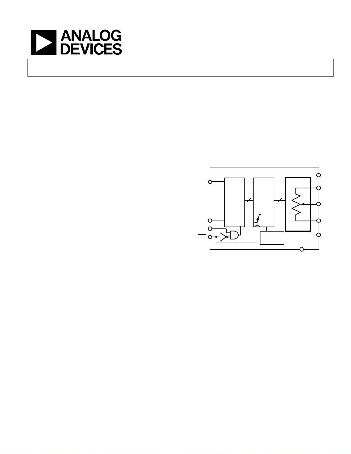
FUNCTIONAL BLOCK DIAGRAM
Q
SDO
SDO
SDI
SDI
CLK
CLK
CS
CS
Q
8-Bit
8-Bit
SERIAL
SERIAL
REG
REG
D
D
CK
CK
88
88
Potentiometer
AD5290
AD5290
AD5290
8-Bit
8-Bit
LATCH
LATCH
RS
RS
POR
POR
GENERAL OVERVIEW
DGND
The AD5290 is a low cost, compact 2.9 mm × 3 mm
+30V/±15V, 256-position digital potentiometer. This device
performs the same electronic adjustment function as
mechanical potentiometers or variable resistors, with enhanced
resolution, solid-state reliability, and superior low temperature
coefficient performance.
The wiper settings are controllable through an SPI compatible
digital interface. The resistance between the wiper and either
end point of the fixed resistor varies linearly with respect to the
digital code transferred into the RDAC latch.
iCMOS™ Process Technology
For analog systems designers within industrial/instrumentation equipment OEMs who need high performance ICs at higher-voltage levels, iCMOS is a
technology platform that enables the development of analog ICs capable of 30V and operating at +/-15V supplies while allowing dramatic reductions in
power consumption and package size, and increased AC and DC performance.
Note:
The terms digital potentiometer and RDAC are used interchangeably.
Figure 1.
DGND
V
V
DD
DD
A
A
W
W
B
B
V
V
SS
SS
Rev. PrE
Information furnished by Analog Devices is believed to be accurate and reliable.
However, no responsibility is assumed by Analog Devices for its use, nor for any
infringements of patents or other rights of third parties that may result from its use.
Specifications subject to change without notice. No license is granted by implication
or otherwise under any patent or patent rights of Anal og Devices. Trademarks and
registered trademarks are the property of their respective companies.
One Technology Way, P.O. Box 9106, Norwood, MA 02062-9106, U.S.A.
Tel: 781.329.4700
Fax: 781.326.8703 © 2005 Analog Devices, Inc. All rights reserved.
www.analog.com

Preliminary Technical Data AD5290
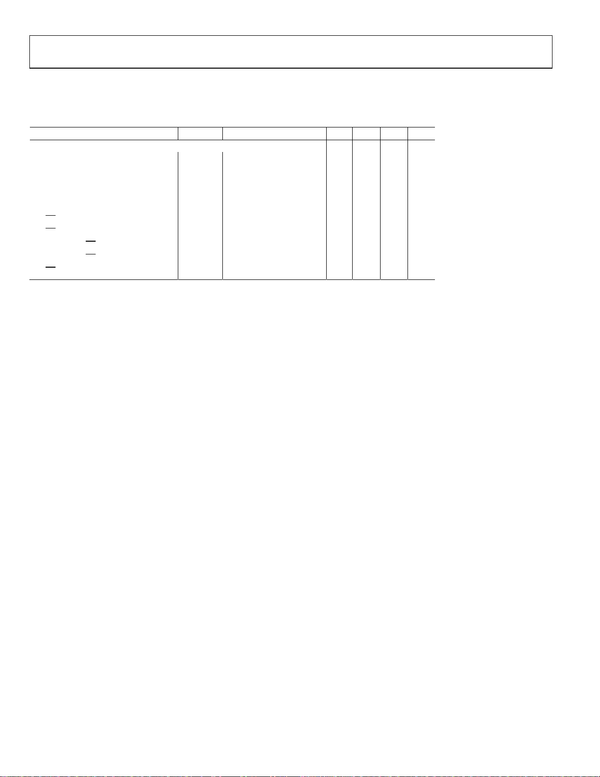
ELECTRICAL CHARACTERISTICS—10 kΩ, 50 kΩ, 100 kΩ VERSIONS
(VDD/VSS = ±15V±10% or ±5V±10%, VA = +VDD, VB = VSS/0V, -40°C < TA < +125°C unless otherwise noted)
Table 1.
Parameter Symbol Conditions Min Typ1 Max Unit
DC CHARACTERISTICS—RHEOSTAT MODE
Resistor Differential Nonlinearity2 R-DNL RWB, V
Resistor Integral Nonlinearity2 R-INL RWB, V
Nominal Resistor Tolerance3 ∆RAB T
Resistance Temperature Coefficient (∆RAB/RAB)/∆T*106
Wiper Resistance RW V
V
DC CHARACTERISTICS—POTENTIOMETER DIVIDER MODE
Resolution N 8 Bits
Differential Nonlinearity4 DNL –1 ±0.1 +1 LSB
Integral Nonlinearity4 INL –1 ±0.3 +1 LSB
Voltage Divider Temperature Coefficient (∆VW/VW)/∆T*106 Code = 0x80 5 ppm/°C
Full-Scale Error V
Zero-Scale Error V
Code = 0xFF –3 –1 0 LSB
WFSE
Code = 0x00 0 1 3 LSB
WZSE
RESISTOR TERMINALS
Voltage Range5 V
Capacitance6 A, B C
V
A,B,W
A,B
Capacitance6 W CW
Common-Mode Leakage ICM V
DIGITAL INPUTS AND OUTPUTS
Input Logic High VIH
Input Logic Low VIL
Output Logic High VOH
Output Logic Low VOL
Input Current II V
Input Capacitance CI 5 pF
POWER SUPPLIES
Power Supply Range
V
/V
SS
DD
Power Supply Range VDD
Supply Current6 IDD
Supply Current IDD
Supply Current ISS
Power Dissipation7 P
DISS
Power Supply Sensitivity PSS
DYNAMIC CHARACTERISTICS
6, 8
Bandwidth –3dB BW
= no connect –1 ±0.1 +1 LSB
A
= no connect –2 ±0.25 +2 LSB
A
= 25°C –30 +30 %
A
V
= VDD,
AB
35 ppm/°C
Wiper = no connect
= ±15 V 60 150 Ω
DD
= ±4.5 V 240 450 Ω
DD
VDD V
SS
f = 1 MHz, measured to
45 pF
GND, Code = 0x80
f = 1 MHz, measured to
60 pF
GND, Code = 0x80
= VB = VW 1 nA
A
V
= +5V or +15V
DD
V
= +5V or +15V
DD
= 2.2 kΩ to +5 V
R
L
IOL = 1.6mA, V
LOGIC
= +5V,
2.4 V
0.8 V
4.9 V
0.4 V
VDD = +15V
= 0 V or +15 V ±1 µA
IN
Dual Supply Range ±4.5 ±16.5 V
+4.5 +30 V
Single Supply Range, V
=
SS
0 V
V
= 5 V or VIL = 0 V, VDD =
IH
0.1 10 µA
+5 V
V
= 5 V or VIL = 0 V, VDD =
IH
0.75 2 mA
+15 V
V
= 5 V or VIL = 0 V, VSS = -
IH
0.02 0.1 mA
5 V or –15 V
= 5 V or VIL = 0 V, VDD =
V
IH
+15 V, V
∆V
∆V
= -15 V
SS
= +15V ±10%, or
DD
= -15V ±10%, Code =
SS
11 30 mW
±0.01 ±0.02 %/%
Midscale
= 10 kΩ/50 kΩ/100 kΩ,
R
AB
525/125/60 kHz
Code = 0x80
Rev. Pr E | Page 2 of 11

Preliminary Technical Data AD5290
Total Harmonic Distortion THDW
VW Settling Time (10 kΩ/50 kΩ/100 kΩ) tS
Resistor Noise Voltage Density e
N_WB
=1 V rms, VB = 0 V,
V
A
f = 1 kHz, R
= 5 V, VB = 0 V,
V
A
= 10 kΩ
AB
±1 LSB error band
R
= 25 kΩ 14 nV/√Hz
WB
0.005 %
4 µs
Rev. Pr E | Page 3 of 11
Preliminary Technical Data AD5290
TIMING CHARACTERISTICS— 10 kΩ, 50 kΩ, 100 kΩ VERSIONS
(VDD/VSS = ±15V±10% or ±5V±10%, VA = +VDD, VB = 0V, -40°C < TA < +125°C unless otherwise noted.)
Table 2.
Parameter Symbol Conditions Min Typ1 Max Unit
SPI INTERFACE TIMING CHARACTERISTICS
Clock Frequency f
Input Clock Pulsewidth tCH, tCL Clock level high or low 120 ns
Data Setup Time tDS 30 ns
Data Hold Time tDH 20 ns
CLK to SDO Propagation Delay tPD
CS Setup Time
CS High Pulsewidth
CLK Fall to CS Fall Hold Time
CLK Fall to CS Rise Hold Time
CS Rise to Clock Rise Setup
NOTES
1. Typical specifications represent average readings at +25°C and V
2. Resistor position nonlinearity error R-INL is the deviation from an ideal value measured between the maximum resistance and the minimum resistance wiper
positions. R-DNL measures the relative step change from ideal between successive tap positions. Parts are guaranteed monotonic.
3. V
= VDD, Wiper (VW) = no connect.
AB
4. INL and DNL are measured at V
5. Resistor terminals A, B, W have no limitations on polarity with respect to each other.
6. Guaranteed by design and not subject to production test.
7. P
8. All dynamic characteristics use V
9. See timing diagram for location of measured values. All input control voltages are specified with t
is calculated from (IDD × VDD+ ISS × VSS) CMOS logic level inputs result in minimum power dissipation.
DISS
of 1.5 V.
with the RDAC configured as a potentiometer divider similar to a voltage output D/A converter. VA=VDD and VB=0 V.
W
/ VSS = ±15 V.
DD
6, 8,9
(Specifications Apply to All Parts)
CLK
R
= 1KΩ, CL < 20pF
PU
t
120 ns
CSS
t
150 ns
CSW
t
TBD ns
CSH0
t
120 ns
CSH1
t
120 ns
CS1
= ±15 V.
DD/VSS
10 100 ns
= tF = 2 ns (10% to 90% of 3 V) and timed from a voltage level
R
4 MHz
Rev. Pr E | Page 4 of 11

Preliminary Technical Data AD5290
ABSOLUTE MAXIMUM RATINGS1
(TA = +25°C, unless otherwise noted.)
Table 3.
Parameter Value
VDD to VSS –0.3 V to +35 V
VDD to GND –0.3 V to +35 V
VSS to GND +0.3 V to –16.5 V
VA, VB, VW to GND VSS , VDD
Maximum Current
I
, IWA Pulsed
WB
I
Continuous (RWB ≤ 1 kΩ, A open)
WB
IWA Continuous (R
≤ 1 kΩ, B open)1
WA
±20 mA
1
±5 mA
±5 mA
Digital Inputs Voltage to GND VDD + 0.3 V
Digital Output Voltage to GND 0 V, +7 V
Operating Temperature Range –40°C to +125°C
Maximum Junction Temperature (T
) 150°C
JMAX
Storage Temperature –65°C to +150°C
Lead Temperature (Soldering, 10 – 30 sec) 245°C
Thermal Resistance2 θJA: MSOP-10 230°C/W
NOTES
1
Maximum terminal current is bounded by the maximum current handling
of the switches, maximum power dissipation of the package, and maximum
applied voltage across any two of the A, B, and W terminals at a given
resistance.
2
Package power dissipation = (T
– TA)/θJA.
JMAX
Stresses above those listed under Absolute Maximum Ratings
may cause permanent damage to the device. This is a stress
rating only and functional operation of the device at these or
any other conditions above those indicated in the operational
section of this specification is not implied. Exposure to
absolute maximum rating conditions for extended periods
may affect device reliability.
Rev. Pr E | Page 5 of 11

Preliminary Technical Data AD5290
PIN CONFIGURATION AND FUNCTION DESCRIPTIONS
1
A
2
B
AD5290
3
VSS
TOP VIEW
4
CS
Figure 2. AD5290 Pin Configuration
Table 7. AD5290 Pin Function Descriptions
Pin Menmonic Description
1 A
2 B
A Terminal. V
B Terminal. V
≤ VA ≤ VDD
SS
≤ VB ≤ VDD
SS
3 VSS Negative Supply. Connect to zero volts for single supply applications.
4 GND Digital Ground.
5
CS
Chip Select Input, Active Low. When
Register
6 CLK Serial Clock Input. Positive edge triggered
7 SDI Serial Data Input Pin. Shifts in one bit at a time on positive clock CLK edges. MSB loaded first.
8 SDO
Serial Data Output Pin. Internal N-Ch FET with open-drain output that requires external pull-
up resistor. It shifts out the previous 8 SDI bits that allows daisy-chain operation of multiple
packages
9 VDD Positive Power Supply
10 W
W Terminal. V
≤ VW ≤ VDD
SS
10
W
VDD
9
8
SDO
SDIGND
7
CLK
65
CS
returns high, data will be loaded into the Wiper
Rev. Pr E | Page 6 of 11

Preliminary Technical Data AD5290
V
SPI Interface
Table 4. AD5290 Serial Data-Word Format
B7 B6 B5 B4 B3 B2 B1 B0
D7 D6 D5 D4 D3 D2 D1 D0
MSB LSB
7
2
2
0
1
SDI
0
1
CLK
0
1
CS
0
1
OUT
0
D7 D6 D5 D4 D3 D2 D1 D0
RDAC REGISTER LOAD
Figure 3. AD5290 SPI Interface Timing Diagram
= VDD, VB = 0 V, VW = V
(V
A
OUT
)
1
SDI
(DATA IN)
CLK
CS
VOUT
0
1
0
t
1
0
V
DD
0
Figure 2. SPI Interface Detailed Timing Diagram (V
Dx Dx
CSH0
t
CSS
t
t
CH
DS
t
CL
t
CH
t
CSH1
t
CS1
t
CSW
t
S
±
1LSB
= VDD, VB = 0 V, VW = V
A
OUT
)
Rev. Pr E | Page 7 of 11

Preliminary Technical Data AD5290
−
OPERATION
The AD5290 is a 256-position digitally controlled variable
resistor device that can be controlled digitally through SPI
interface.
An internal power-on preset places the wiper at midscale
during power-on, which simplifies the fault condition recovery
at power-up.
DETERMINING THE VARIABLE RESISTANCE
AND VOLTAGE
Rheostat Mode Operation
If only the W-to-B or W-to-A terminals are used as variable
resistors, the unused terminal can be opened or shorted with W.
This operation is called rheostat mode (Figure 3).
A
W
B
Figure 3. Rheostat Mode Configuration
The nominal resistance (RAB) of the RDAC has 256 contact
points accessed by the wiper terminal, plus the B terminal
contact if R
is considered. The 8-bit data in the RDAC latch is
WB
decoded to select one of the 256 settings. Assuming that a 10
kΩ part is used, the wiper’s first connection starts at the B
terminal for data 0x00. Such connection yields a minimum of
60 Ω resistance between terminals W and B because of the 60 Ω
wiper contact resistance. The second connection is the first tap
point, which corresponds to 99 Ω (R
for data 0x01, and so on. Each LSB data value increase moves
the wiper up the resistor ladder until the last tap point is reached
at 10020 Ω ((255) × R
diagram of the equivalent RDAC circuit. The general equation
determining R
WB
is
)D(R +×= (1)
where:
D is the decimal equivalent of the 8-bit binary code.
R
is the end-to-end resistance.
AB
is the wiper resistance contributed by the on-resistance of
R
W
the internal switch.
Table 1. R
the A Terminal Is Opened
D (Dec) RWB (Ω) Output State
255 10020 Full-Scale (RAB + RW)
128 5060 Midscale
1 99 1 LSB
0 60 Zero-Scale (Wiper Contact Resistance)
vs. Codes; RAB = 10 kΩ and
WB
A
W
B
/256 + RW). Figure 6 shows a simplified
AB
D
RR
256
A
W
B
= (1) × RAB/256 + RW)
WB
WABWB
03437-0-050
Since a finite wiper resistance of 60 Ω is present in the zeroscale condition, care should be taken to limit the current flow
between W and B in this state to a maximum pulse current of
no more than 20 mA. Otherwise, degradation or possible
destruction of the internal switch contact can occur.
Similar to the mechanical potentiometer, the resistance of the
RDAC between the wiper W and terminal A also produces a
complementary resistance R
. When these terminals are used,
WA
the B terminal can be opened or shorted to W. Setting the
resistance value for R
starts at a maximum value of resistance
WA
and decreases as the data loaded in the latch increases in value.
The general equation for this operation is
Table 2. R
)D(R +×
=
D256
256
vs. Codes; RAB =10 kΩ and
WA
(2)
RR
WABWA
B Terminal Is Opened
D (Dec) RWA (Ω) Output State
255 60 Full-Scale
128 5060 Midscale
1 10020 1 LSB
0 10060 Zero-Scale
The typical distribution of the resistance tolerance from device
to device is process lot dependent, and it is possible to have
±30% tolerance.
A
R
S
D7
D6
D5
D4
D3
D2
D1
D0
DECODER
Figure 6. AD5290 Equivalent RDAC Circuit
RDAC
LATCH
AND
R
S
R
S
W
R
W
R
S
B
Potentiometer Mode Operation
If all three terminals are used, the operation is called the
potentiometer mode. The most common configuration is the
voltage divider operation (Figure 7).
Rev. Pr E | Page 8 of 11

Preliminary Technical Data AD5290
The data setup and data hold times in the specification table
V
I
A
W
V
O
B
03437-0-051
Figure 7. Potentiometer Mode Configuration
Ignoring the effect of the wiper resistance, the transfer function
is simply
D
256
V
AW
)D(V = (3)
A more accurate calculation, which includes the wiper
resistance effect, yields
D
256
)D(V
=
W
R
AB
RR
+
WAB
(4)
V
R2
+
A
W
determine the valid timing requirements. The AD5290 uses an
8-bit serial input data register word that is transferred to the
CS
internal RDAC register when the
returns to logic high. If
dataword contains more than 8-bit, the extra MSB bits will be
ignored.
ESD PROTECTION
All digital inputs are protected with a series input resistor and
parallel Zener ESD structures shown in 8 and Figure 9. This
CS
applies to the digital input pins SDI, CLK, and
340Ω
Figure 8. ESD Protection of Digital Pins
A,B,W
LOGIC
V
SS
.
If there is an applied voltage at the B terminal, then the transfer
function becomes
D
DV
W
V
)(
256
A
D
−
256
+=
256
(5)
V
B
Unlike in rheostat mode operation where the absolute tolerance
is high, potentiometer mode operation yields an almost ratiometric function of D/256 with a relatively small error contributed
by the RW terms, and therefore the tolerance effect is almost
cancelled. Although the thin film step resistor R
switches resistance R
have very different temperature coeffi-
W
and CMOS
S
cients, the ratiometric adjustment also reduces the overall
temperature coefficient effect to 5 ppm/°C, except at low value
codes where R
dominates.
W
Potentiometer mode operations include others such as op amp
input, feedback resistor networks, and other voltage scaling
applications. A, W, and B terminals can in fact be input or
output terminals provided that |V
exceed |V
| and |VSS|.
DD
|, |VW|, and |VB| do not
A
SPI COMPATIBLE 3-WIRE SERIAL BUS
The AD5290 contains a 3-wire SPI compatible digital interface
CS
(SDI,
first. The format of the word is shown in Table .
The positive-edge sensitive CLK input requires clean transitions
to avoid clocking incorrect data into the serial input register.
Standard logic families work well.
goes low, the clock loads data into the serial register on each
positive clock edge (see Figure 3).
, and CLK). The 8-bit serial word must be loaded MSB
CS
should start high, when it
V
SS
Figure 9. ESD Protection of Resistor Terminals
TERMINAL VOLTAGE OPERATING RANGE
The AD5290 VDD and GND power supply defines the boundary
conditions for proper 3-terminal digital potentiometer
operation. Supply signals present on terminals A, B, and W that
exceed V
or GND will be clamped by the internal forward
DD
biased diodes (see Figure 10).
V
DD
A
W
B
V
SS
Figure 10. Maximum Terminal Voltages Set by V
DD
and V
SS
POWER-UP SEQUENCE
Since the ESD protection diodes limit the voltage compliance at
terminals A, B, and W (see Figure 10), it is important to power
–to-GND and VSS-to-GND before applying any voltage to
V
DD
terminals A, B, and W; otherwise, the diode will be forward
biased such that V
affect the rest of the user’s circuit. The ideal power-up sequence
is in the following order: GND, V
will be powered unintentionally and may
DD
, digital inputs, and then
SS,VDD
Rev. Pr E | Page 9 of 11

Preliminary Technical Data AD5290
A
A
V
. The relative order of powering VA, VB, VW, and the
A/B/W
digital inputs is not important as long as they are powered after
and VSS with respect to GND.
V
DD
m
V
D D
LAYOUT AND POWER SUPPLY BYPASSING
It is a good practice to employ compact, minimum lead length
layout design. The leads to the inputs should be as direct as
possible with a minimum conductor length. Ground paths
should have low resistance and low inductance.
Similarly, it is also a good practice to bypass the power supplies
with quality capacitors for optimum stability. Supply leads to
the device should be bypassed with disc or chip ceramic
capacitors of 0.01 µF to 0.1 µF. Low ESR 1 µF to 10 µF tantalum
or electrolytic capacitors should also be applied at the supplies
to minimize any transient disturbance and low frequency ripple
(see Figure 1111). Note that the digital ground should also be
joined remotely to the analog ground at one point to minimize
the ground bounce.
AD5290
Figure 11. Power Supply Bypassing
DAISY CHAIN OPERATION
The serial data output pin (SDO) can be used to daisy chain
multiple devices for simultaneous operations, see Figure 12. The
SDO pin contains an open drain N-Ch FET and requires a pullup resistor. Users need to tie the SDO pin of one package to the
SDI pin of the next package. If many devices are daisy-chained,
users may need to increase the clock period to accommodate
the time delay introduced by the pull-up resistors and the
capacitive loading at the SDO-SDI interface, see Figure 12.
If two AD5290 are daisy chained, this requires total 16 bits of
data. The first 8 bits goes to U2 and the second 8 bits goes to
CS
U1. The
their respective serial registers. The
complete the operation.
should be kept low until all 16 bits are clocked into
CS
is then pulled high to
D5290
uC
SCLK
MOSI
SS
U1 U2
SDI S D O
CS CLK
Figure 12. Daisy Chain Configuration
R
p
2 . 2 K
D5290
Ω
S D I SDO
CS CLK
Rev. Pr E | Page 10 of 11

Preliminary Technical Data AD5290
PR04716-0-2/05(PrE)
OUTLINE DIMENSIONS
3.00 BSC
6
10
3.00 BSC
1
PIN 1
0.50 BSC
0.95
0.85
0.75
0.15
0.00
0.27
0.17
COPLANARITY
0.10
COMPLIANT TO JEDEC STANDARDS MO-187BA
Figure 13. 10-Lead Mini Small Outline Package [MSOP]
Ordering Guide
Model1 R
AD5290YRMZ10 10 –40°C to +125°C MSOP-10 RM-10 D4U
AD5290YRMZ10-RL7 10 –40°C to +125°C MSOP-10 RM-10 D4U
AD5290YRMZ50 50 –40°C to +125°C MSOP-10 RM-10 D4T
AD5290YRMZ50-RL7 50 –40°C to +125°C MSOP-10 RM-10 D4T
AD5290YRMZ100 100 –40°C to +125°C MSOP-10 RM-10 D4V
AD5290YRMZ100-RL7 100 –40°C to +125°C MSOP-10 RM-10 D4V
AD5290EVAL 10 Evaluation Board
NOTES:
1. Z in Model Number denotes Lead Free Package
Purchase of licensed I2C components of Analog Devices or one of its sublicensed Associated Companies conveys a license for the purchaser under the Philips I2C Patent
Rights to use these components in an I2C system, provided that the system conforms to the I2C Standard Specification as defined by Philips.
(kΩ) Temperature Range Package Description Package Option Branding
AB
4.90 BSC
5
1.10 MAX
SEATING
PLANE
0.23
0.08
(RM-10)
Dimensions shown in millimeters
8°
0°
0.80
0.60
0.40
ESD CAUTION
ESD (electrostatic discharge) sensitive device. Electrostatic charges as high as 4000 V readily accumulate on the
human body and test equipment and can discharge without detection. Although this product features
proprietary ESD protection circuitry, permanent damage may occur on devices subjected to high energy
electrostatic discharges. Therefore, proper ESD precautions are recommended to avoid performance
degradation or loss of functionality.
Rev. Pr E | Page 11 of 11
 Loading...