

I2C-Compatible,
A
A
FEATURES
256 positions
10 kΩ, 100 kΩ, 1 MΩ
Low temperature coefficient: 30 ppm/°C
Internal power on midscale preset
Single-supply 2.7 V to 5.5 V or dual-supply ±2.7 V for ac or
bipolar operation
2
I
C-compatible interface with readback capability
Extra programmable logic outputs
Self-contained shutdown feature
Extended temperature range: −40°C to +105°C
APPLICATIONS
Multimedia, video, and audio
Communications
Mechanical potentiometer replacement
Instrumentation: gain, offset adjustment
Programmable voltage-to-current conversion
Line impedance matching
256-Position Digital Potentiometers
AD5241/AD5242
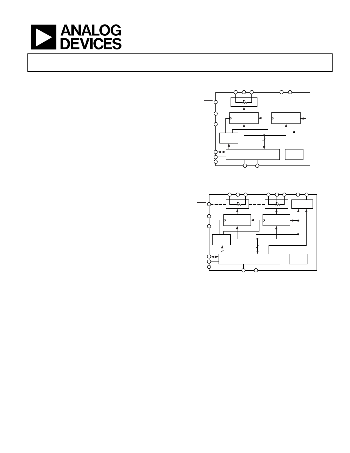
FUNCTIONAL BLOCK DIAGRAM
O1O
2
REGISTER 2
8
PWR-ON
RESET
A2W2B2O1O
REGISTER
00926-001
2
SHDN
1W1B1
SHDN
V
V
SDA
SCL
GND
DD
SS
DECODE
RDAC
REGIS TER 1
ADDR
AD5241
SERIAL INPUT REGIST ER
AD0
AD1
Figure 1. AD5241 Functional Block Diagram
1W1B1
GENERAL DESCRIPTION
The AD5241/AD5242 provide a single-/dual-channel, 256position, digitally controlled variable resistor (VR) device. These
devices perform the same electronic adjustment function as a
potentiometer, trimmer, or variable resistor. Each VR offers a
completely programmable value of resistance between the A
terminal and the wiper, or the B terminal and the wiper. For the
AD5242, the fixed A-to-B terminal resistance of 10 kΩ, 100 kΩ,
or 1 MΩ has a 1% channel-to-channel matching tolerance. The
nominal temperature coefficient of both parts is 30 ppm/°C.
V
V
SDA
SCL
GND
DD
SS
DECODE
RDAC
REGISTER 1
ADDR
AD5242
1
SERIAL INPUT REGISTER
AD0 AD1
REGISTER 2
8
RDAC
PWR-ON
RESET
00926-002
Figure 2. AD5242 Functional Block Diagram
Wiper position programming defaults to midscale at system
power on. When powered, the VR wiper position is programmed
2
by an I
C®-compatible, 2-wire serial data interface. Both parts
have two extra programmable logic outputs available that
enable users to drive digital loads, logic gates, LED drivers, and
analog switches in their system.
The AD5241/AD5242 are available in surface-mount, 14-lead
SOIC and 16-lead SOIC packages and, for ultracompact solutions,
14-lead TSSOP and 16-lead TSSOP packages. All parts are
guaranteed to operate over the extended temperature range of
−40°C to +105°C.
Rev. C
Information furnished by Analog Devices is believed to be accurate and reliable. However, no
responsibility is assumed by Analog Devices for its use, nor for any infringements of patents or other
rights of third parties that may result from its use. Specifications subject to change without notice. No
license is granted by implication or otherwise under any patent or patent rights of Analog Devices.
Trademarks and registered trademarks are the property of their respective owners.
One Technology Way, P.O. Box 9106, Norwood, MA 02062-9106, U.S.A.
Tel: 781.329.4700 www.analog.com
Fax: 781.461.3113 ©2001–2009 Analog Devices, Inc. All rights reserved.

AD5241/AD5242
TABLE OF CONTENTS
Features .............................................................................................. 1
Applications ....................................................................................... 1
Functional Block Diagram .............................................................. 1
General Description ......................................................................... 1
Revision History ............................................................................... 2
Specifications ..................................................................................... 3
10 kΩ, 100 kΩ, 1 MΩ Version .................................................... 3
Timing Diagrams .......................................................................... 5
Absolute Maximum Ratings ............................................................ 6
ESD Caution .................................................................................. 6
Pin Configurations and Function Descriptions ........................... 7
Typical Performance Characteristics ............................................. 8
REVISION HISTORY
12/09—Rev. B to Rev. C
Changes to Features Section............................................................ 1
Changes to 10 kΩ, 100 kΩ, 1 MΩ Version Section ...................... 3
Changes to Table 3 ............................................................................ 6
Deleted Digital Potentiometer Selection Guide Section ........... 14
Changed Self-Contained Shutdown Function Section to
Shutdown Function Section .......................................................... 15
Changes to Shutdown Function Section ..................................... 15
Changes to Ordering Guide .......................................................... 18
8/02—Rev. A to Rev. B
Additions to Features ....................................................................... 1
Changes to General Description .................................................... 1
Changes to Specifications ................................................................ 2
Changes to Absolute Maximum Ratings ....................................... 4
Additions to Ordering Guide .......................................................... 4
Changes to TPC 8 and TPC 9 ......................................................... 8
Changes to Readback RDAC Value Section ................................ 11
Changes to Additional Programmable Logic Output Section .. 11
Added Self-Contained Shutdown Section ................................... 12
Added Figure 8 ................................................................................ 12
Changes to Digital Potentiometer Selection Guide ................... 14
Test Circuits ..................................................................................... 11
Theory of Operation ...................................................................... 12
Programming the Variable Resistor ......................................... 12
Programming the Potentiometer Divider ............................... 13
Digital Interface .......................................................................... 13
Readback RDAC Value .............................................................. 14
Multiple Devices on One Bus ................................................... 14
Level-Shift for Bidirectional Interface ..................................... 14
Additional Programmable Logic Output ................................ 15
Shutdown Function .................................................................... 15
Outline Dimensions ....................................................................... 16
Ordering Guide .......................................................................... 18
2/02—Rev. 0 to Rev. A
Edits to Features ................................................................................. 1
Edits to Functional Block Diagrams ............................................... 1
Edits to Absolute Maximum Ratings .............................................. 4
Changes to Ordering Guide ............................................................. 4
Edits to Pin Function Descriptions ................................................. 5
Edits to Figures 1, 2, 3 ....................................................................... 6
Added Readback RDAC Value Section, Additional
Programmable Logic Output Section, and Figure 7;
Renumbered Sequentially ............................................................. 11
Changes to Digital Potentiometer Selection Guide ................... 14
Rev. C | Page 2 of 20

AD5241/AD5242
V
SPECIFICATIONS
10 kΩ, 100 kΩ, 1 MΩ VERSION
VDD = 2.7 V to 5.5 V, VA = VDD, VB = 0 V, −40°C < TA < +105°C, unless otherwise noted.
Table 1.
Parameter Symbol Conditions Min Typ1 Max Unit
DC CHARACTERISTICS, RHEOSTAT MODE
(SPECIFICATIONS APPLY TO ALL VRs)
Resolution N 8 Bits
Resistor Differential Nonlinearity2 R-DNL RWB, VA = no connect −1 ±0.4 +1 LSB
Resistor Integral Nonlinearity2 R-INL RWB, VA = no connect −2 ±0.5 +2 LSB
Nominal Resistor Tolerance ΔRAB/RAB T
Resistance Temperature Coefficient
Wiper Resistance RW I
DC CHARACTERISTICS, POTENTIOMETER DIVIDER
MODE (SPECIFICATIONS APPLY TO ALL VRs)
Resolution N 8 Bits
Differential Nonlinearity3 DNL −1 ±0.4 +1 LSB
Integral Nonlinearity3 INL −2 ±0.5 +2 LSB
Voltage Divider Temperature Coefficient (ΔVW/VW)/∆T × 106 Code = 0x80 5 ppm/°C
Full-Scale Error V
Zero-Scale Error V
RESISTOR TERMINALS
Voltage Range4 V
Capacitance (A, B)5 C
Capacitance (W)5 C
Common-Mode Leakage ICM V
DIGITAL INPUTS
Input Logic High (SDA and SCL) VIH 0.7 × VDD VDD + 0.5 V V
Input Logic Low (SDA and SCL) VIL −0.5 +0.3 × VDD V
Input Logic High (AD0 and AD1) VIH V
Input Logic Low (AD0 and AD1) VIL V
Input Logic High VIH V
Input Logic Low VIL V
Input Current IIL V
Input Capacitance5 C
DIGITAL OUTPUT
Output Logic Low (SDA) VOL I
Output Logic Low (O1 and O2) VOL I
Output Logic High (O1 and O2) VOH I
Three-State Leakage Current (SDA) IOZ V
Output Capacitance5 C
POWER SUPPLIES
Power Single-Supply Range V
Power Dual-Supply Range VDD/V
Positive Supply Current IDD V
Negative Supply Current ISS V
Power Dissipation6 P
Power Supply Sensitivity PSS −0.01 +0.002 +0.01 %/%
= 25°C, RAB = 10 kΩ −30 +30 %
A
−30 +50 %
30 ppm/°C
(ΔR
AB/RAB
ΔT × 10
= 25°C,
T
A
= 100 kΩ/1 MΩ
R
AB
)/
6
= VDD, wiper =
V
AB
no connect
= VDD/R 60 120 Ω
W
Code = 0xFF −1 −0.5 0 LSB
WFSE
Code = 0x00 0 0.5 1 LSB
WZSE
, VB, VW V
A
A
, CB
f = 1 MHz, measured
V
SS
V
DD
45 pF
to GND, code = 0x80
W
f = 1 MHz, measured
60 pF
to GND, code = 0x80
= VB = VW 1 nA
A
= 5 V 2.4 VDD V
DD
= 5 V 0 0.8 V
DD
= 3 V 2.1 VDD V
DD
= 3 V 0 0.6 V
DD
= 5 V or VIL = GND 1 μA
IH
3 pF
IL
OL
3 8 pF
OZ
V
DD RANGE
±2.3 ±2.7 V
SS RANGE
DISS
IOL= 3 mA 0.4 V
= 6 mA 0.6 V
OL
= 1.6 mA 0.4 V
SINK
= 40 μA 4 V
SOURCE
= 5 V or VIL = GND ±1 μA
IH
= 0 V 2.7 5.5 V
SS
= 5 V or VIL = GND 0.1 50 μA
IH
= −2.5 V, VDD = +2.5 V +0.1 −50 μA
SS
= 5 V or VIL = GND,
V
IH
V
= 5 V
DD
0.5 250
μW
Rev. C | Page 3 of 20

AD5241/AD5242
Parameter Symbol Conditions Min Typ1 Max Unit
DYNAMIC CHARACTERISTICS
−3 dB Bandwidth BW_10 kΩ RAB = 10 kΩ, code = 0x80 650 kHz
BW_100 kΩ RAB = 100 kΩ, code = 0x80 69 kHz
BW_1 MΩ RAB = 1 MΩ, code = 0x80 6 kHz
Total Harmonic Distortion THDW
VW Settling Time tS
Resistor Noise Voltage e
INTERFACE TIMING CHARACTERISTICS
(APPLIES TO ALL PARTS
SCL Clock Frequency f
Bus Free Time Between Stop and Start, t
5, 7 , 8
0.005 %
2 μs
5, 9
= 1 V rms + 2 V dc,
V
A
= 2 V dc, f = 1 kHz
V
B
= VDD, VB = 0 V, ± 1 LSB
V
A
error band, R
R
N_WB
= 5 kΩ, f = 1 kHz 14 nV√Hz
WB
= 10 kΩ
AB
)
0 400 kHz
SCL
t1 1.3 μs
BUF
Hold Time (Repeated Start), t
t
HD; STA
2
After this period, the first
600 ns
clock pulse is generated
Low Period of SCL Clock, t
High Period of SCL Clock, t
Setup Time for Repeated Start Condition, t
Data Hold Time, t
Data Setup Time, t
HD; DAT
SU; DAT
t
LOW
t
HIGH
SU; STA
t
t
1.3 μs
3
0.6 50 μs
4
t5 600 ns
900 ns
6
100 ns
7
Rise Time of Both SDA and SCL Signals, tR t8 300 ns
Fall Time of Both SDA and SCL Signals, tF t9 300 ns
Setup Time for Stop Condition, t
1
Typicals represent average readings at 25°C, VDD = 5 V.
2
Resistor position nonlinearity error R-INL is the deviation from an ideal value measured between the maximum resistance and the minimum resistance wiper
positions. R-DNL measures the relative step change from ideal between successive tap positions. Parts are guaranteed monotonic. See Test Circuits.
3
INL and DNL are measured at VW with the RDAC configured as a potentiometer divider similar to a voltage output D/A converter. VA = VDD and VB = 0 V. DNL
specification limits of ±1 LSB maximum are guaranteed monotonic operating conditions. See Figure 37.
4
Resistor Terminal A, Resistor Terminal B, and Resistor Terminal W have no limitations on polarity with respect to each other.
5
Guaranteed by design, not subject to production test.
6
P
is calculated from (IDD × VDD). CMOS logic level inputs result in minimum power dissipation.
DISS
7
Bandwidth, noise, and settling time are dependent on the terminal resistance value chosen. The lowest R value results in the fastest settling time and highest
bandwidth. The highest R value results in the minimum overall power consumption.
8
All dynamic characteristics use VDD = 5 V.
9
See timing diagram in Figure 3 for location of measured values.
t
SU; STO
10
Rev. C | Page 4 of 20
AD5241/AD5242
SDA
S
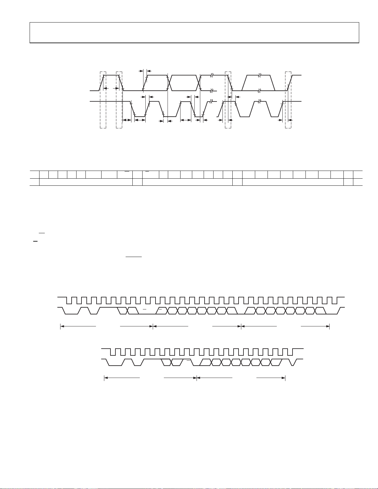
TIMING DIAGRAMS
t
8
t
1
t
8
t
9
t
2
SCL
t
2
t
SP
3
t
t
4
6
t
7
t
5
S P
t
10
Figure 3. Detail Timing Diagram
Data of AD5241/AD5242 is accepted from the I
2
C bus in the following serial format.
Table 2.
S 0 1 0 1 1 AD1 AD0
Slave Address Byte Instruction Byte Data Byte
W
R/
A
/B
A
RS SD O
O2 X X X A D7 D6 D5 D4 D3 D2 D1 D0 A P
1
where:
S = start condition
P = stop condition
A = acknowledge
X = don’t care
AD1, AD0 = Package pin programmable address bits. Must be matched with the logic states at Pins AD1 and AD0.
W
R/
= Read enable at high and output to SDA. Write enable at low.
A
/B = RDAC subaddress select; 0 for RDAC1 and 1 for RDAC2.
RS = Midscale reset, active high.
SD = Shutdown in active high. Same as
O
, O2 = Output logic pin latched values
1
SHDN
except inverse logic.
D7, D6, D5, D4, D3, D2, D1, D0 = data bits.
SCL
SDA
TART BY
MASTER
1 119 99
0
0
1
SLAVE ADDRESS BYT E
1
FRAME 1
1
AD1 AD0
R/W
A/B D0D4D5D6D7 D3 D2 D1
ACK BY
AD5241
SDRS
OO
21
FRAME 2
INSTRUCTIO N BYTE
XXX
ACK BY
AD5241
Figure 4. Writing to the RDAC Serial Register
SCL
SDA
START BY
MASTER
1
0
0
1
SLAVE ADDRESS BYTE
11
FRAME 1
AD1 AD0
R/W
D6 D5 D4 D3 D2 D1 D0
D7
ACK BY
AD5241
DATA BYTE FROM PREVIO USLY SELECTED
RDAC REGISTER I N WRITE MO DE
FRAME 2
Figure 5. Reading Data from a Previously Selected RDAC Register in Write Mode
FRAME 3
DATA BYTE
919
NO ACK BY
MASTER
STOP BY
MASTER
0926-005
ACK BY
AD5241
STOP BY
MASTER
0926-007
00926-006
Rev. C | Page 5 of 20
AD5241/AD5242
ABSOLUTE MAXIMUM RATINGS
TA = 25°C, unless otherwise noted.
Table 3.
Parameter Rating
VDD to GND −0.3 V to +7 V
VSS to GND 0 V to −7 V
VDD to VSS 7 V
VA, VB, VW to GND VSS to VDD
IA, IB, IW
RAB = 10 kΩ in TSSOP-14 5.0 mA1
RAB = 100 kΩ in TSSOP-14 1.5 mA1
RAB = 1 MΩ in TSSOP-14 0.5 mA1
Digital Input Voltage to GND 0 V to VDD + 0.3 V
Operating Temperature Range −40°C to +105°C
Thermal Resistance θJA
14-Lead SOIC 158°C/W
16-Lead SOIC 73°C/W
14-Lead TSSOP 206°C/W
16-Lead TSSOP 180°C/W
Maximum Junction Temperature (TJ max) 150°C
Package Power Dissipation PD = (TJ max − TA)/θJA
Storage Temperature Range −65°C to +150°C
Lead Temperature
Vapor Phase, 60 sec 215°C
Infrared, 15 sec 220°C
1
Maximum current increases at lower resistance and different packages.
Stresses above those listed under Absolute Maximum Ratings
may cause permanent damage to the device. This is a stress
rating only; functional operation of the device at these or any
other conditions above those indicated in the operational
section of this specification is not implied. Exposure to absolute
maximum rating conditions for extended periods may affect
device reliability.
ESD CAUTION
Rev. C | Page 6 of 20
AD5241/AD5242
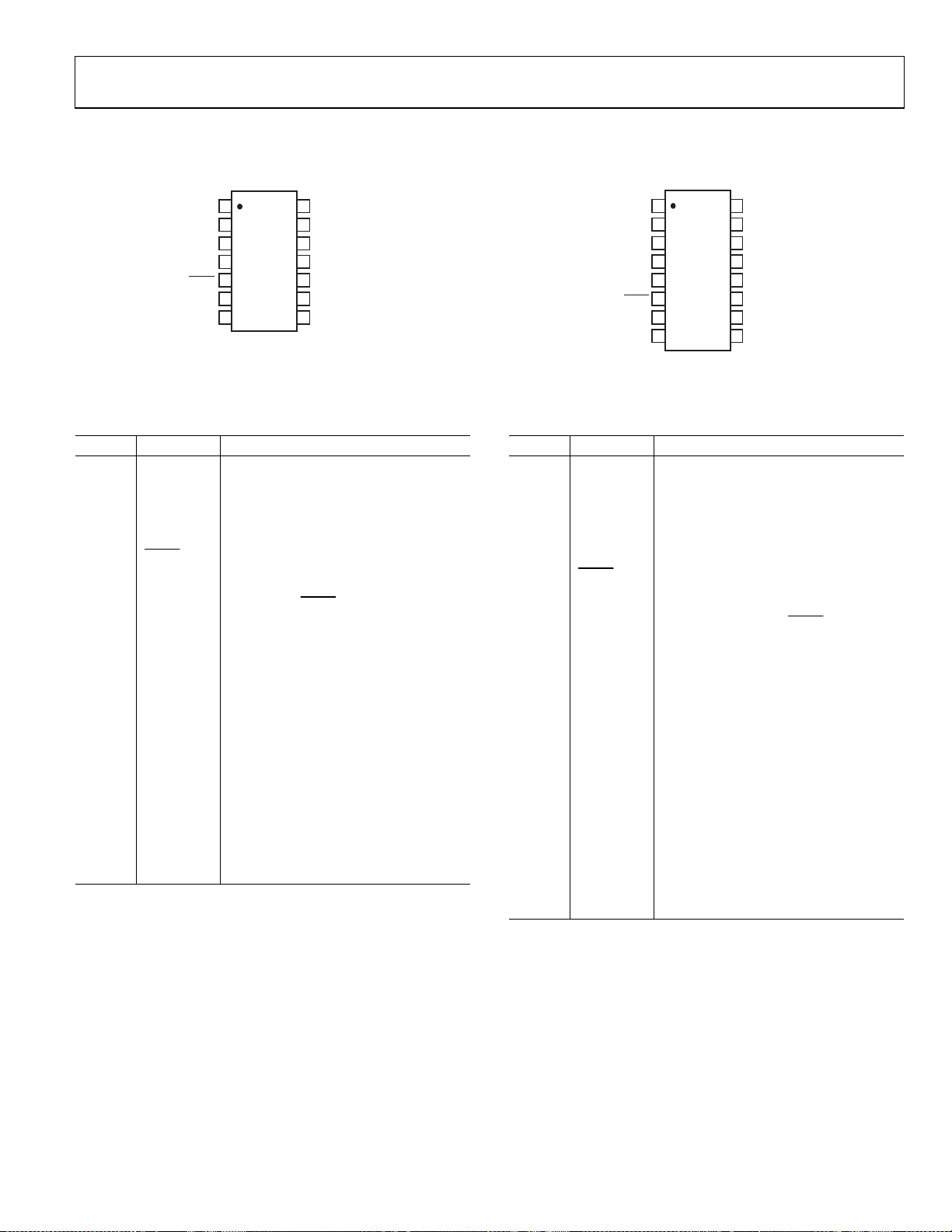
PIN CONFIGURATIONS AND FUNCTION DESCRIPTIONS
1
A
1
2
W
1
3
B
1
4
V
DD
5
SHDN
6
SCL
7
SDA
NC = NO CONNECT
AD5241
TOP VIEW
(Not to Scale)
14
O
1
13
NC
12
O
2
11
V
SS
10
DGND
9
AD1
8
AD0
00926-003
Figure 6. AD5241 Pin Configuration
Table 4. AD5241 Pin Function Descriptions
Pin No. Mnemonic Description
1 A1 Resistor Terminal A1.
2 W1 Wiper Terminal W1.
3 B1 Resistor Terminal B1.
4 VDD
Positive Power Supply, Specified for
Operation from 2.2 V to 5.5 V.
5
Active low, asynchronous connection of
SHDN
Wiper W to Terminal B, and open circuit
of Terminal A. RDAC register contents
unchanged. SHDN should tie to VDD
if not used.
6 SCL Serial Clock Input.
7 SDA Serial Data Input/Output.
8 AD0
Programmable Address Bit for Multiple
Package Decoding. Bit AD0 and Bit AD1
provide four possible addresses.
9 AD1
Programmable Address Bit for Multiple
Package Decoding. Bit AD0 and Bit AD1
provide four possible addresses.
10 DGND Common Ground.
11 VSS
Negative Power Supply, Specified for
Operation from 0 V to −2.7 V.
12 O2 Logic Output Terminal O2.
13 NC No Connect.
14 O1 Logic Output Terminal O1.
16
15
14
13
12
11
10
9
A
2
W
2
B
2
O
2
V
SS
DGND
AD1
AD0
00926-004
W
V
SHDN
SCL
SDA
O
1
A
1
1
B
1
DD
1
2
3
AD5242
4
TOP VIEW
5
(Not to Scale)
6
7
8
Figure 7. AD5242 Pin Configuration
Table 5. AD5242 Pin Function Descriptions
Pin No. Mnemonic Description
1 O1 Logic Output Terminal O1.
2 A1 Resistor Terminal A1.
3 W
4 B
5 V
Wiper Terminal W1.
1
Resistor Terminal B1.
1
DD
Positive Power Supply, Specified for
Operation from 2.2 V to 5.5 V.
6
Active Low, Asynchronous Connection
SHDN
of Wiper W to Terminal B, and Open
Circuit of Terminal A. RDAC register
contents unchanged. SHDN should
7 SCL
8 SDA
9 AD0
tie to V
Serial Clock Input.
Serial Data Input/Output.
Programmable Address Bit for Multiple
, if not used.
DD
Package Decoding. Bit AD0 and Bit AD1
provide four possible addresses.
10 AD1
Programmable Address Bit for Multiple
Package Decoding. Bit AD0 and Bit AD1
provide four possible addresses.
11 DGND
12 V
SS
Common Ground.
Negative Power Supply, Specified for
Operation from 0 V to −2.7 V.
13 O
14 B
15 W
16 A
Logic Output Terminal O2.
2
Resistor Terminal B2.
2
Wiper Terminal W2.
2
Resistor Terminal A2.
2
Rev. C | Page 7 of 20
AD5241/AD5242
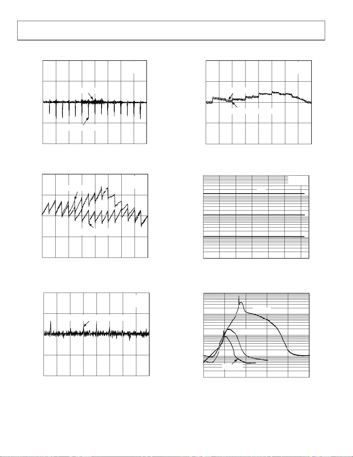
TYPICAL PERFORMANCE CHARACTERISTICS
1.0
V
DD
V
DD
V
DD
= +2.7V
= +5.5V
= ±2.7V
0.50
VDD = +2.7V
V
= +5.5V
DD
V
= ±2.7V
DD
0.5
VDD/VSS = +2.7V/0V
0
NONLINEARITY (LSB)
–0.5
RHEOSTAT MODE DIFFERENTIAL
–1.0
V
DD/VSS
= +5.5V/0V, ±2.7V
CODE (Decimal)
256
2241921601289664320
0926-008
Figure 8. RDNL vs. Code
1.0
VDD/VSS = +2.7V/0V
0.5
0
NONLINEARITY (LSB)
–0.5
RHEOSTAT MODE INTEGRAL
VDD/VSS = +5.5V/0V, ±2.7V
VDD = +2.7V
= +5.5V
V
DD
= ±2.7V
V
DD
0.25
VDD/VSS = +2.7V
0
V
= +2.7V/0V, +5.5V/0V
DD/VSS
POTENTIOMETER MODE
–0.25
INTEGRAL NONLINEARITY (LSB)
–0.50
128
64320196 92
CODE (Decimal)
160
224
256
00926-011
Figure 11. INL vs. Code
10k
1k
100
10
NOMINAL RESISTANCE (kΩ)
1MΩ
100kΩ
10kΩ
VDD = 2.7V
T
= 25°C
A
–1.0
CODE (Decimal)
256
2241921601289664320
0926-009
Figure 9. RINL vs. Code
0.25
0.13
0
POTENTIOMETER MODE
–0.13
DIFFERENTIAL NONLINEARITY (LSB)
–0.25
VDD/VSS = +2.7V/0V, +5.5V/0V, ±2.7V
CODE (Dec imal)
VDD = +2.7V
= +5.5V
V
DD
= ±2.7V
V
DD
2241921601289664320
256
00926-010
Figure 10. DNL vs. Code
1
TEMPERATURE ( °C)
806040200–20–40
00926-012
Figure 12. Nominal Resistance vs. Temperature
10k
VDD = 3V
VDD = 5V
54321
00926-013
1k
A)
µ
100
SUPPLY CURRENT (
DD
10
I
VDD = 2.5V
1
0
INPUT LOGIC VOLTAGE (V)
Figure 13. Supply Current vs. Input Logic Voltage
Rev. C | Page 8 of 20

AD5241/AD5242
A)
µ
(
SHUTDOWN CURRENT
0.1
0.01
0.001
–40
–20
0
20
TEMPERATURE (°C)
RAB= 10k
VDD = 5.5V
6040
80
Figure 14. Shutdown Current vs. Temperature
70
60
10MΩ VERSION
50
40
30
20
10
0
–10
–20
POTENTI OMETER MO DE TEMPCO ( ppm/°C)
–30
10kΩ VERSION
100kΩ VERSION
CODE (Decimal)
1289664320
160 192 224 256
V
DD/VSS
= 25°C
T
A
= 2.7V/0V
Figure 15. ΔVWB/ΔT Potentiometer Mode Temperature Coefficient
120
100
80
pm/°C)
60
40
20
0
–20
–40
RHEOSTAT MODE TEMPCO (p
–60
–80
100kΩ VERSION
10kΩ VERSION
10MΩ VERSION
9664320
CODE (Decimal)
VDD/VSS = 2.7V/0V
T
A
160128
192
= 25°C
224
256
Figure 16. ΔRWB/ΔT Rheostat Mode Temperature Coefficient
Ω
0926-014
0926-015
00926-016
100
TA = 25°C
90
80
70
60
50
40
30
WIPER RESISTANCE (Ω)
20
10
COMMON-MO DE (V)
Figure 17. Incremental Wiper Contact vs. VDD/VSS
300
A: VDD/VSS = 5.5V/0V
250
200
150
SUPPLY CURRENT (µA)
100
DD
I
50
0
10
CODE = 0xFF
B: V
CODE = 0xFF
C: V
CODE = 0xFF
D: V
CODE = 0x55
E: V
CODE = 0x55
F: V
CODE = 0x55
DD/VSS
DD/VSS
DD/VSS
DD/VSS
DD/VSS
= 3.3V/0V
= 2.5V/0V
= 5.5V/0V
= 3.3V/0V
= 2.5V/0V
FREQUENCY (kHz)
Figure 18. Supply Current vs. Frequency
6
0
–6
–12
–18
–24
GAIN (dB)
–30
–36
–42
–48
–54
100
0xFF
0x80
0x40
0x20
0x10
0x08
0x04
0x02
0x01
FREQUENCY (Hz)
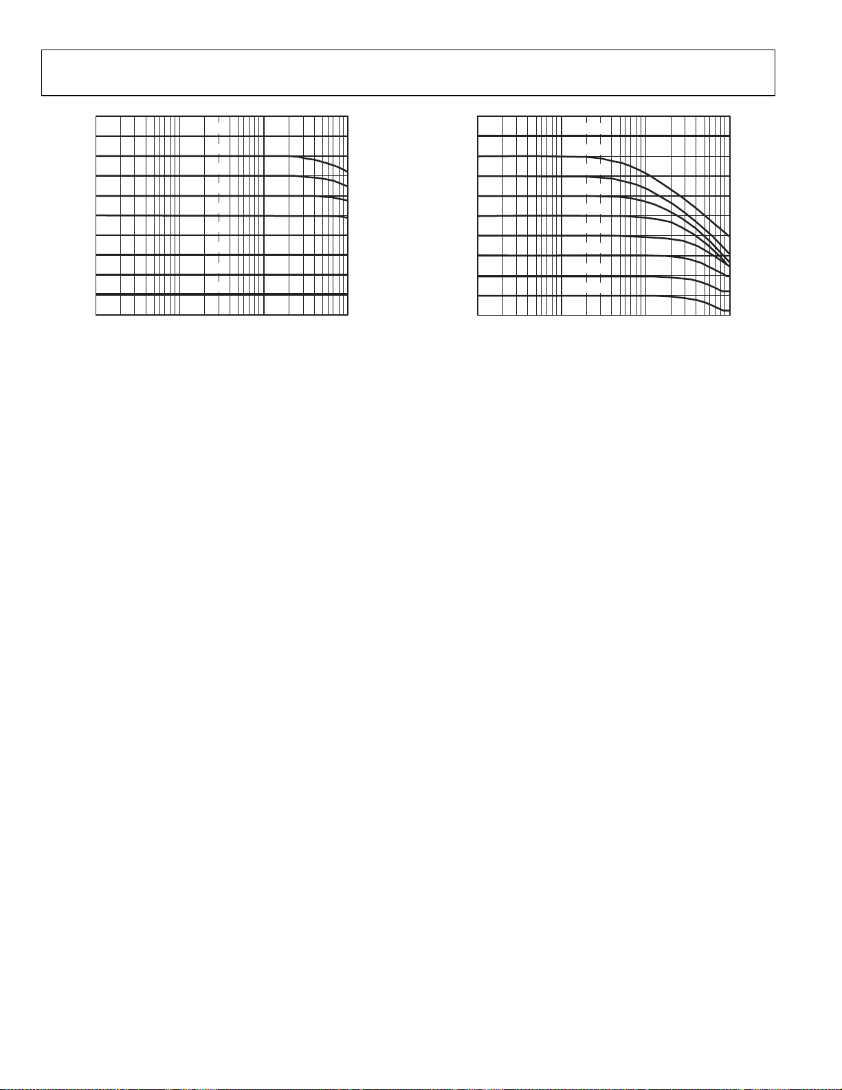
Figure 19. AD5242 10 k Ω Gain vs. Frequency vs. Code
VDD/VSS = +2.7V/0V
VDD/VSS = ±2.7V/0V
VDD/VSS = +5.5V/0V
543210–1–2–3
100k10k1k
1M
6
00926-017
D
A
E
B
F
C
1k100
00926-019
00926-018
Rev. C | Page 9 of 20
AD5241/AD5242
6
0
–6
–12
–18
–24
GAIN (dB)
–30
–36
–42
–48
–54
100
0xFF
0x80
0x40
0x20
0x10
0x08
0x04
0x02
0x01
FREQUENCY (Hz)
100k10k1k
00926-020
Figure 20. AD5242 100 kΩ Gain vs. Frequency vs. Code
6
0
–6
–12
–18
–24
GAIN (dB)
–30
–36
–42
–48
–54
0xFF
0x80
0x40
0x20
0x10
0x08
0x04
0x02
0x01
FREQUENCY (Hz)
100k10k1k100
00926-021
Figure 21. AD5242 1 MΩ Gain vs. Frequency vs. Code
Rev. C | Page 10 of 20

AD5241/AD5242
V
V
O
V
TEST CIRCUITS
Figure 22 to Figure 30 define the test conditions used in the product specifications table.
5
DUT
A
V+
W
B
V+ = V
DD
1 LSB = V+/ 2
V
MS
Figure 22. Potentiometer Divider Nonlinearity Error (INL, DNL)
NO CONNE CT
DUT
A
B
W
I
W
V
MS
Figure 23. Resistor Position Nonlinearity Error
(Rheostat Operation; R-INL, R-DNL)
DUT
A
V
MS2
W
B
IW = VDD/R
V
W
V
MS1
RW = [V
NOMIN AL
MS1
Figure 24. Wiper Resistance
A
V
DD
A
V+
W
B
V+ = V
±10%
DD
PSRR (dB) = 20 LO G
PSS (%/%) =
V
MS
Figure 25. Power Supply Sensitivity (PSS, PSRR)
DUT
OFFSET
BIAS
B
5V
W
OP279
OFFSET
GND
A
Figure 26. Inverting Gain
Δ
VMS%
Δ
VDD%
N
– V
DUT
OP279
W
B
V
IN
OFFSET
GND
0926-029
A
OFFSET
BIAS
V
OUT
00926-034
Figure 27. Noninverting Gain
A
V
FFSET
GND
00926-030
DUT
IN
2.5V
B
+15V
W
OP42
–15V
V
OUT
00926-035
Figure 28. Gain vs. Frequency
0.1
RSW =
I
CODE = 0x00
VSS TO V
SW
0.1V
DD
00926-036
MS2
DUT
W
B
I
SW
]/I
W
00926-031
Figure 29. Incremental On Resistance
NC
Δ
V
MS
Δ
V
DD
0926-032
V
DUT
V
GND
NC
A
W
B
DD
SS
I
CM
V
CM
00926-037
Figure 30. Common-Mode Leakage Current
V
OUT
00926-033
Rev. C | Page 11 of 20

AD5241/AD5242
−
THEORY OF OPERATION
The AD5241/AD5242 provide a single-/dual-channel, 256position digitally controlled variable resistor (VR) device. The
terms VR, RDAC, and programmable resistor are commonly
used interchangeably to refer to digital potentiometer.
To program the VR settings, refer to the Digital Interface section.
Both parts have an internal power-on preset that places the wiper
in midscale during power-on that simplifies the fault condition
recovery at power-up. In addition, the shutdown pin (
SHDN
)
of AD5241/AD5242 places the RDAC in an almost zero power
consumption state where Terminal A is open circuited and Wiper
W is connected to Terminal B, resulting in only leakage current
being consumed in the VR structure. During shutdown, the VR
latch contents are maintained when the RDAC is inactive. When
the part returns from shutdown, the stored VR setting is applied
to the RDAC.
A
SHDN
SW
SHDN
D7
D6
D5
D4
D3
D2
D1
D0
RDAC
LATCH
AND
DECODER
R
R
R
R
Figure 31. Equivalent RDAC Circuit
N
SW
2–1
N
SW
2–2
SW
1
SW
0
DIGITAL CIRCUITRY
B
OMITT ED FOR CLARIT Y
W
RR
N
/2
AB
00926-022
PROGRAMMING THE VARIABLE RESISTOR
Rheostat Operation
The nominal resistance of the RDAC between Terminal A and
Terminal B is available in 10 kΩ, 100 kΩ, and 1 MΩ. The final two
or three digits of the part number determine the nominal resistance
value, for example, 10 kΩ = 10, 100 kΩ = 100, and 1 MΩ = 1 M.
The nominal resistance (R
accessed by the wiper terminal, plus the B terminal contact. The
8-bit data in the RDAC latch is decoded to select one of the 256
possible settings. Assume a 10 kΩ part is used; the first connection
of the wiper starts at the B terminal for Data 0x00. Because there is
a 60 Ω wiper contact resistance, such connection yields a minimum
of 60 Ω resistance between Terminal W and Terminal B. The
second connection is the first tap point that corresponds to 99 Ω
(R
= RAB/256 + RW = 39 + 60) for Data 0x01. The third connection
WB
is the next tap point representing 138 Ω (39 × 2 + 60) for Data 0x02,
and so on. Each LSB data value increase moves the wiper up the
resistor ladder until the last tap point is reached at 10,021 Ω
[R
– 1 LSB + RW].
AB
) of the VR has 256 contact points
AB
Figure 31 shows a simplified diagram of the equivalent RDAC
circuit where the last resistor string is not accessed; therefore,
there is 1 LSB less of the nominal resistance at full scale in
addition to the wiper resistance.
The general equation determining the digitally programmed
resistance between W and B is
(D) =
D
256
× R
+ RW (1)
AB
R
WB
where:
D is the decimal equivalent of the binary code between 0 and 255,
which is loaded in the 8-bit RDAC register.
is the nominal end-to-end resistance.
R
AB
is the wiper resistance contributed by the on resistance of
R
W
the internal switch.
Again, if R
tied to W. Tabl e 6 shows the R
= 10 kΩ, Terminal A can be either open circuit or
AB
resistance based on the code
WB
set in the RDAC latch.
Table 6. RWB (D) at Selected Codes for RAB = 10 kΩ
D (DEC) RWB (Ω) Output State
255 10021 Full-scale (RWB – 1 LSB + RW)
128 5060 Midscale
1 99 1 LSB
0 60 Zero-scale (wiper contact resistance)
Note that in the zero-scale condition, a finite wiper resistance of
60 Ω is present. Care should be taken to limit the current flow
between W and B in this state to a maximum current of no more
than 20 mA. Otherwise, degradation or possible destruction of
the internal switch contact can occur.
Similar to the mechanical potentiometer, the resistance of the
RDAC between Wiper W and Terminal A also produces a
digitally controlled resistance, R
. When these terminals are
WA
used, Terminal B can be opened or tied to the wiper terminal.
The minimum R
resistance is for Data 0xFF and increases as
WA
the data loaded in the latch decreases in value. The general
equation for this operation is
256 D
(D) =
R
WA
= 10 kΩ, Terminal B can be either open circuit or tied
For R
AB
to W. Ta ble 7 shows the R
× RAB + RW (2)
256
resistance based on the code set in
WA
the RDAC latch.
Table 7. RWA (D) at Selected Codes for RAB = 10 kΩ
D (DEC) RWA (Ω) Output State
255 99 Full-scale
128 5060 Midscale
1 10021 1 LSB
0 10060 Zero-scale
Rev. C | Page 12 of 20

AD5241/AD5242
The typical distribution of the nominal resistance RAB from
channel to channel matches within ±1% for AD5242. Deviceto-device matching is process lot dependent, and it is possible to
have ±30% variation. Because the resistance element is processed in
thin film technology, the change in R
with temperature has no
AB
more than a 30 ppm/°C temperature coefficient.
PROGRAMMING THE POTENTIOMETER DIVIDER
Voltage Output Operation
The digital potentiometer easily generates output voltages at
wiper-to-B and wiper-to-A to be proportional to the input
voltage at A-to-B. Unlike the polarity of V
be positive, voltage across terminal A to terminal B, terminal W
to terminal A, and terminal W to terminal B can be at either
polarity provided that V
is powered by a negative supply.
SS
If ignoring the effect of the wiper resistance for approximation,
connecting Terminal A to 5 V and Terminal B to ground produces
an output voltage at the wiper-to-B starting at 0 V up to 1 LSB less
than 5 V. Each LSB of voltage is equal to the voltage applied across
Terminal AB divided by the 256 positions of the potentiometer
divider. Because AD5241/AD5242 can be supplied by dual
supplies, the general equation defining the output voltage at V
with respect to ground for any valid input voltage applied to
Terminal A and Terminal B is
()
W
D
256
V
A
DV
D
256
−
256
V
B
+=
which can be simplified to
()
W
DV +=
D
256
(4)
VV
B
AB
where D is the decimal equivalent of the binary code between 0
to 255 that is loaded in the 8-bit RDAC register.
For a more accurate calculation, including the effects of wiper
resistance, V
where R
can be found as
W
()
DV
W
(D) and RWA(D) can be obtained from Equation 1 and
WB
V
R
A
AB
DR
)(
WB
DR
WA
+=
R
AB
Equation 2.
Operation of the digital potentiometer in divider mode results
in a more accurate operation over temperature. Unlike rheostat
mode, the output voltage is dependent on the ratio of the internal
resistors, R
and RWB, and not the absolute values; therefore,
WA
the temperature drift reduces to 5 ppm/°C.
/VSS, which must
DD
W
(3)
)(
(5)
V
B
Rev. C | Page 13 of 20
DIGITAL INTERFACE
2-Wire Serial Bus
The AD5241/AD5242 are controlled via an I2C-compatible
serial bus. The RDACs are connected to this bus as slave devices.
Referring to Figure 3 and Figure 4, the first byte of AD5241/
AD5242 is a slave address byte. It has a 7-bit slave address and
W
bit. The five MSBs are 01011 and the following two bits
an R/
are determined by the state of the AD0 and AD1 pins of the
device. AD0 and AD1 allow users to use up to four of these
devices on one bus.
The 2-wire, I
1.
The master initiates a data transfer by establishing a start
condition, which is when a high-to-low transition on the SDA
line occurs while SCL is high (see Figure 4). The following
byte is the Frame 1, slave address byte, which consists of the
7-bit slave address followed by an R/
whether data is read from or written to the slave device).
The slave whose address corresponds to the transmitted
address responds by pulling the SDA line low during the
ninth clock pulse (this is the acknowledge bit). At this stage,
all other devices on the bus remain idle while the selected
device waits for data to be written to or read from its serial
register. If the R/
slave device. If the R/
slave device.
A write operation contains an extra instruction byte more
2.
than the read operation. The Frame 2 instruction byte in
write mode follows the slave address byte. The MSB of the
instruction byte labeled
low selects RDAC1 and a high selects RDAC2 for the dualchannel AD5242. Set
second MSB, RS, is the midscale reset. A logic high of this
bit moves the wiper of a selected RDAC to the center tap
where R
logic high on SD causes the RDAC to open circuit at
Terminal A while shorting the wiper to Terminal B. This
operation yields almost a 0 Ω rheostat mode or 0 V in
potentiometer mode. This SD bit serves the same function
as the
low. The following two bits are O
programmable logic outputs that users can use to drive
other digital loads, logic gates, LED drivers, analog switches,
and the like. The three LSBs are don’t care (see ). Figure 4
After acknowledging the instruction byte, the last byte in
3.
write mode is the, Frame 3 data byte. Data is transmitted
over the serial bus in sequences of nine clock pulses (eight
data bits followed by an acknowledge bit). The transitions
on the SDA line must occur during the low period of SCL
and remain stable during the high period of SCL (see Figure 4).
2
C serial bus protocol operates as follows:
W
bit (this bit determines
W
bit is high, the master reads from the
W
bit is low, the master writes to the
A
/B is the RDAC subaddress select. A
A
/B to low for the AD5241. The
= RWB. The third MSB, SD, is a shutdown bit. A
WA
SHDN
pin except that the
SHDN
pin reacts to active
and O1. They are extra
2

AD5241/AD5242
V
V
V
V
V
4. Unlike the write mode, the data byte follows immediately
after the acknowledgment of the slave address byte in
Frame 2 read mode. Data is transmitted over the serial bus
in sequences of nine clock pulses (slightly different from
the write mode, there are eight data bits followed by a no
acknowledge Logic 1 bit in read mode). Similarly, the
transitions on the SDA line must occur during the low
period of SCL and remain stable during the high period of
SCL (see Figure 5).
When all data bits have been read or written, a stop condition
5.
is established by the master. A stop condition is defined as
a low-to-high transition on the SDA line while SCL is high.
In write mode, the master pulls the SDA line high during
the tenth clock pulse to establish a stop condition (see
Figure 4). In read mode, the master issues a no acknowledge
for the ninth clock pulse (that is, the SDA line remains high).
The master then brings the SDA line low before the tenth
clock pulse, which goes high to establish a stop condition
(see Figure 5).
A repeated write function gives the user flexibility to update the
RDAC output a number of times after addressing and instructing
the part only once. During the write cycle, each data byte updates
the RDAC output. For example, after the RDAC has acknowledged
its slave address and instruction bytes, the RDAC output is
updated. If another byte is written to the RDAC while it is still
addressed to a specific slave device with the same instruction,
this byte updates the output of the selected slave device. If
different instructions are needed, the write mode has to start a
completely new sequence with a new slave address, instruction,
and data bytes transferred again. Similarly, a repeated read
function of the RDAC is also allowed.
READBACK RDAC VALUE
Specific to the AD5242 dual-channel device, the channel of
interest is the one that was previously selected in the write mode.
In addition, to read both RDAC values consecutively, users have to
perform two write-read cycles. For example, users may first specify
the RDAC1 subaddress in write mode (it is not necessary to issue
the data byte and stop condition), and then change to read mode
to read the RDAC1 value. To continue reading the RDAC2 value,
users have to switch back to write mode, specify the subaddress,
and then switch once again to read mode to read the RDAC2
value. It is not necessary to issue the write mode data byte or
the first stop condition for this operation. Users should refer to
Figure 4 and Figure 5 for the programming format.
5
RPR
P
MASTER
V
SDA SCL
AD1
AD0
AD5242
DD
SDA SCL
AD1
AD0
AD5242
Figure 33. Multiple AD5242 Devices on One Bus
MULTIPLE DEVICES ON ONE BUS
Figure 33 shows four AD5242 devices on the same serial bus.
Each has a different slave address because the state of their AD0
and AD1 pins are different. This allows each RDAC within each
device to be written to or read from independently. The master
device output bus line drivers are open-drain pull-downs in a
2
C-compatible interface. Note, a device is addressed properly
fully I
only if the bit information of AD0 and AD1 in the slave address
byte matches with the logic inputs at the AD0 and AD1 pins of
that particular device.
LEVEL-SHIFT FOR BIDIRECTIONAL INTERFACE
While most old systems can operate at one voltage, a new
component may be optimized at another. When they operate
the same signal at two different voltages, a proper method of
level-shifting is needed. For instance, a 3.3 V E
used to interface with a 5 V digital potentiometer. A level-shift
scheme is needed to enable a bidirectional communication so that
the setting of the digital potentiometer can be stored to and
2
retrieved from the E
PROM. Figure 32 shows one of the techniques.
M1 and M2 can be N-channel FETs (2N7002) or low threshold
FDV301N if V
= 3.3
DD
SDA1
SCL1
Figure 32. Level-Shift for Different Voltage Devices Operation
falls below 2.5 V.
DD
RPR
3.3V
2
PROM
E
G
P
SD
M1
G
SD
M2
SDA
SCL
V
DD
SDA SCL
AD1
AD0
AD5242
V
DD
SDA SCL
AD1
AD0
AD5242
0926-023
2
PROM can be
RPR
P
5V
AD5242
DD
= 5
SDA2
SCL2
0926-024
Rev. C | Page 14 of 20

AD5241/AD5242
V
A
ADDITIONAL PROGRAMMABLE LOGIC OUTPUT
The AD5241/AD5242 feature additional programmable logic
outputs, O
switches, and logic gates. They can also be used as a self-contained
shutdown preset to Logic 0 that is further explained in the
Shutdown Function section. O
power-up. The logic states of O
Frame 2 under the write mode (see Figure 4). Figure 34 shows
the output stage of O
channel MOSFETs in push-pull configuration. As shown in
Figure 34, the output is equal to V
outputs have adequate current driving capability to drive
milliamperes of load.
Users can also activate O1 and O2 in the following three different
ways without affecting the wiper settings:
1.
Start, slave address byte, acknowledge, instruction byte
Complete the write cycle with stop, then start, slave address
2.
Do not complete the write cycle by not issuing the stop,
3.
All digital inputs are protected with a series input resistor and
the parallel Zener ESD structures shown in Figure 36. This
applies to the digital input pins, SDA, SCL, and
and O2, that can be used to drive digital load, analog
1
and O2 default to Logic 0 during
1
and O2 can be programmed in
1
, which employs large P-channel and N-
1
or VSS, and these logic
DD
DD
M
P
1 2
IN
O1DATA IN FRAME 2
OF WRITE MODE
M
N
Figure 34. Output Stage of Logic Output, O
O
1
V
SS
00926-025
1
and O2 specified, acknowledge, stop.
with O
1
byte, acknowledge, instruction byte with O
and O2 specified,
1
acknowledge, stop.
then start, slave address byte, acknowledge, instruction
byte with O
and O2 specified, acknowledge, stop.
1
SHDN
.
SHUTDOWN FUNCTION
0926-026
00926-027
00926-028
SHDN
pin or
1
Shutdown can be activated by strobing the
programming the SD bit in the write mode instruction byte (see
). If the RDAC Register 1 or RDAC Register 2 (AD5242
Tabl e 2
only) is placed in shutdown mode by the software, SD bit, the
part returns the wiper to its prior position when a new command
is received.
In addition, shutdown can be implemented with the device digital
output, as shown in Figure 35. In this configuration, the device
is shutdown during power-up but users are allowed to program
the device. Thus, when O
is programmed high, the device exits
1
shutdown mode and responds to the new setting. This self-contained
shutdown function allows absolute shutdown during power-up,
which is crucial in hazardous environments, and it does not add
extra components.
O
1
SHDN
R
PD
SDA
SCL
Figure 35. Shutdown by Internal Logic Output, O
340
Ω
LOGIC
V
SS
Figure 36. ESD Protection of Digital Pins
,B,W
V
SS
Figure 37. ESD Protection of Resistor Terminals
Rev. C | Page 15 of 20
AD5241/AD5242
OUTLINE DIMENSIONS
5.10
5.00
4.90
4.50
4.40
4.30
PIN 1
1.05
1.00
0.80
0.15
0.05
COPLANARITY
0.10
14
1
0.65 BSC
0.30
0.19
COMPLIANT TO JEDEC STANDARDS MO-153-AB-1
8
6.40
BSC
7
1.20
0.20
MAX
SEATING
PLANE
0.09
8°
0°
0.75
0.60
0.45
061908-A
Figure 38. 14-Lead Thin Shrink Small Outline Package [TSSOP]
(RU-14)
Dimensions shown in millimeters
8.75 (0.3445)
8.55 (0.3366)
BSC
8
6.20 (0.2441)
5.80 (0.2283)
7
1.75 (0.0689)
1.35 (0.0531)
SEATING
PLANE
8°
0°
0.25 (0.0098)
0.17 (0.0067)
0.50 (0.0197)
0.25 (0.0098)
1.27 (0.0500)
0.40 (0.0157)
45°
4.00 (0.1575)
3.80 (0.1496)
0.25 (0.0098)
0.10 (0.0039)
COPLANARIT Y
0.10
14
1
1.27 (0.0500)
0.51 (0.0201)
0.31 (0.0122)
CONTROLL ING DIMENSIONS ARE IN MILLIMETERS; INCH DI MENSIONS
(IN PARENTHESES) ARE ROUNDED-O FF MIL LIMETE R EQUIVALENTS FOR
REFERENCE ON LY AND ARE NOT APPROPRI ATE FOR USE IN DESIGN.
COMPLIANT TO JEDEC STANDARDS MS-012-AB
060606-A
Figure 39. 14-Lead Standard Small Outline Package [SOIC_N]
Narrow Body
(R-14)
Dimensions shown in millimeters and (inches)
Rev. C | Page 16 of 20

AD5241/AD5242
4.50
4.40
4.30
PIN 1
0.15
0.05
0.65
BSC
5.10
5.00
4.90
16
COPLANARITY
COMPLIANT TO JEDEC STANDARDS MO-153-AB
0.10
0.30
0.19
9
81
1.20
MAX
SEATING
PLANE
6.40
BSC
0.20
0.09
8°
0°
0.75
0.60
0.45
Figure 40. 16-Lead Thin Shrink Small Outline Package [TSSOP]
(RU-16)
Dimensions shown in millimeters
10.00 (0.3937)
9.80 (0.3858)
4.00 (0.1575)
3.80 (0.1496)
16
1
9
8
6.20 (0.2441)
5.80 (0.2283)
0.25 (0.0098)
0.10 (0.0039)
COPLANARITY
0.10
CONTROLL ING DIMENSIONS ARE IN MILLIMETERS; INCH DI MENSIONS
(IN PARENTHESES) ARE ROUNDED-O FF MIL LIMET ER EQUIVALENTS FOR
REFERENCE ON LY AND ARE NOT APPROPRI ATE FOR USE IN DESIGN.
1.27 (0.0500)
BSC
0.51 (0.0201)
0.31 (0.0122)
COMPLIANT TO JEDEC STANDARDS MS-012-AC
1.75 (0.0689)
1.35 (0.0531)
SEATING
PLANE
0.25 (0.0098)
0.17 (0.0067)
8°
0°
0.50 (0.0197)
0.25 (0.0098)
1.27 (0.0500)
0.40 (0.0157)
45°
060606-A
Figure 41. 16-Lead Standard Small Outline Package [SOIC_N]
Narrow Body
(R-16)
Dimensions shown in millimeters and (inches)
Rev. C | Page 17 of 20

AD5241/AD5242
ORDERING GUIDE
1, 2
Model
AD5241BR10 1 10 kΩ –40°C to +105°C 14-Lead SOIC_N R-14
AD5241BR10-REEL7 1 10 kΩ –40°C to +105°C 14-Lead SOIC_N R-14
AD5241BRZ10 1 10 kΩ –40°C to +105°C 14-Lead SOIC_N R-14
AD5241BRZ10-RL7 1 10 kΩ –40°C to +105°C 14-Lead SOIC_N R-14
AD5241BRU10 1 10 kΩ –40°C to +105°C 14-Lead TSSOP RU-14
AD5241BRU10-REEL7 1 10 kΩ –40°C to +105°C 14-Lead TSSOP RU-14
AD5241BRUZ10 1 10 kΩ –40°C to +105°C 14-Lead TSSOP RU-14
AD5241BRUZ10-R7 1 10 kΩ –40°C to +105°C 14-Lead TSSOP RU-14
AD5241BR100 1 100 kΩ –40°C to +105°C 14-Lead SOIC_N R-14
AD5241BR100-REEL7 1 100 kΩ –40°C to +105°C 14-Lead SOIC_N R-14
AD5241BRZ100 1 100 kΩ –40°C to +105°C 14-Lead SOIC_N R-14
AD5241BRZ100-RL7 1 100 kΩ –40°C to +105°C 14-Lead SOIC_N R-14
AD5241BRU100 1 100 kΩ –40°C to +105°C 14-Lead TSSOP RU-14
AD5241BRU100-REEL7 1 100 kΩ –40°C to +105°C 14-Lead TSSOP RU-14
AD5241BRUZ100 1 100 kΩ –40°C to +105°C 14-Lead TSSOP RU-14
AD5241BRUZ100-R7 1 100 kΩ –40°C to +105°C 14-Lead TSSOP RU-14
AD5241BR1M 1 1 MΩ –40°C to +105°C 14-Lead SOIC_N R-14
AD5241BRZ1M 1 1 MΩ –40°C to +105°C 14-Lead SOIC_N R-14
AD5241BRZ1M-REEL 1 1 MΩ –40°C to +105°C 14-Lead SOIC_N R-14
AD5241BRU1M 1 1 MΩ –40°C to +105°C 14-Lead SOIC_N R-14
AD5241BRU1M-REEL7 1 1 MΩ –40°C to +105°C 14-Lead TSSOP RU-14
AD5241BRUZ1M 1 1 MΩ –40°C to +105°C 14-Lead TSSOP RU-14
AD5241BRUZ1M-R7 1 1 MΩ –40°C to +105°C 14-Lead TSSOP RU-14
AD5242BR10 2 10 kΩ –40°C to +105°C 16-Lead SOIC_N R-16
AD5242BR10-REEL7 2 10 kΩ –40°C to +105°C 16-Lead SOIC_N R-16
AD5242BRZ10 2 10 kΩ –40°C to +105°C 16-Lead SOIC_N R-16
AD5242BRZ10-REEL7 2 10 kΩ –40°C to +105°C 16-Lead SOIC_N R-16
AD5242BRU10 2 10 kΩ –40°C to +105°C 16-Lead TSSOP RU-16
AD5242BRU10-REEL7 2 10 kΩ –40°C to +105°C 16-Lead TSSOP RU-16
AD5242BRUZ10 2 10 kΩ –40°C to +105°C 16-Lead TSSOP RU-16
AD5242BRUZ10-RL7 2 10 kΩ –40°C to +105°C 16-Lead TSSOP RU-16
AD5242BR100 2 100 kΩ –40°C to +105°C 16-Lead SOIC_N R-16
AD5242BR100-REEL7 2 100 kΩ –40°C to +105°C 16-Lead SOIC_N R-16
AD5242BRZ100 2 100 kΩ –40°C to +105°C 16-Lead SOIC_N R-16
AD5242BRZ100-REEL7 2 100 kΩ –40°C to +105°C 16-Lead SOIC_N R-16
AD5242BRU100 2 100 kΩ –40°C to +105°C 16-Lead TSSOP RU-16
AD5242BRU100-REEL7 2 100 kΩ –40°C to +105°C 16-Lead TSSOP RU-16
AD5242BRUZ100 2 100 kΩ –40°C to +105°C 16-Lead TSSOP RU-16
AD5242BRUZ100-RL7 2 100 kΩ –40°C to +105°C 16-Lead TSSOP RU-16
AD5242BR1M 2 1 MΩ
AD5242BRZ1M 2 1 MΩ –40°C to +105°C 16-Lead SOIC_N R-16
AD5242BRU1M 2 1 MΩ –40°C to +105°C 16-Lead SOIC_N R-16
AD5242BRU1M-REEL7 2 1 MΩ –40°C to +105°C 16-Lead TSSOP RU-16
AD5242BRUZ1M 2 1 MΩ –40°C to +105°C 16-Lead TSSOP RU-16
AD5242BRUZ1M-REEL7 2 1 MΩ –40°C to +105°C 16-Lead TSSOP RU-16
EVAL-AD5242EBZ 2 Evaluation Board
1
The AD5241/AD5242 die size is 69 mil × 78 mil, 5,382 sq. mil. Contains 386 transistors for each channel. Patent Number 5,495,245 applies.
2
Z = RoHS Compliant Part.
No. of Channels End-to-End RAB Temperature Range Package Description Package Option
–40°C to +105°C
16-Lead SOIC_N R-16
Rev. C | Page 18 of 20

AD5241/AD5242
NOTES
Rev. C | Page 19 of 20

AD5241/AD5242
NOTES
©2001–2009 Analog Devices, Inc. All rights reserved. Trademarks and
registered trademarks are the property of their respective owners.
D00926-0-12/09(C)
Rev. C | Page 20 of 20
 Loading...