

Precision
www.BDTIC.com/ADI
FEATURES
Low noise: 0.3 μV p-p at 0.1 Hz to 10 Hz
Low nonlinearity: 0.003% (G = 1)
High CMRR: 120 dB (G = 1000)
Low offset voltage: 50 μV
Low offset voltage drift: 0.5 μV/°C
Gain bandwidth product: 25 MHz
Pin programmable gains of 1, 10, 100, 1000
Input protection, power-on/power-off
No external components required
Internally compensated
MIL-STD-883B and chips available
16-lead ceramic DIP and SOIC packages and 20-terminal
leadless chip carrier available
Available in tape and reel in accordance with EIA-481A
standard
Standard military drawing also available
GENERAL DESCRIPTION
The AD524 is a precision monolithic instrumentation amplifier
designed for data acquisition applications requiring high accuracy under worst-case operating conditions. An outstanding
combination of high linearity, high common-mode rejection,
low offset voltage drift, and low noise makes the AD524 suitable
for use in many data acquisition systems.
The AD524 has an output offset voltage drift of less than
25 μV/°C, input offset voltage drift of less than 0.5 μV/°C, CMR
above 90 dB at unity gain (120 dB at G = 1000), and maximum
nonlinearity of 0.003% at G = 1. In addition to the outstanding
dc specifications, the AD524 also has a 25 kHz bandwidth
(G = 1000). To make it suitable for high speed data acquisition
systems, the AD524 has an output slew rate of 5 V/μs and settles
in 15 μs to 0.01% for gains of 1 to 100.
As a complete amplifier, the AD524 does not require any external components for fixed gains of 1, 10, 100 and 1000. For other
gain settings between 1 and 1000, only a single resistor is required.
The AD524 input is fully protected for both power-on and
power-off fault conditions.
The AD524 IC instrumentation amplifier is available in four
different versions of accuracy and operating temperature range.
The economical A grade, the low drift B grade, and lower drift,
Instrumentation Amplifier
AD524
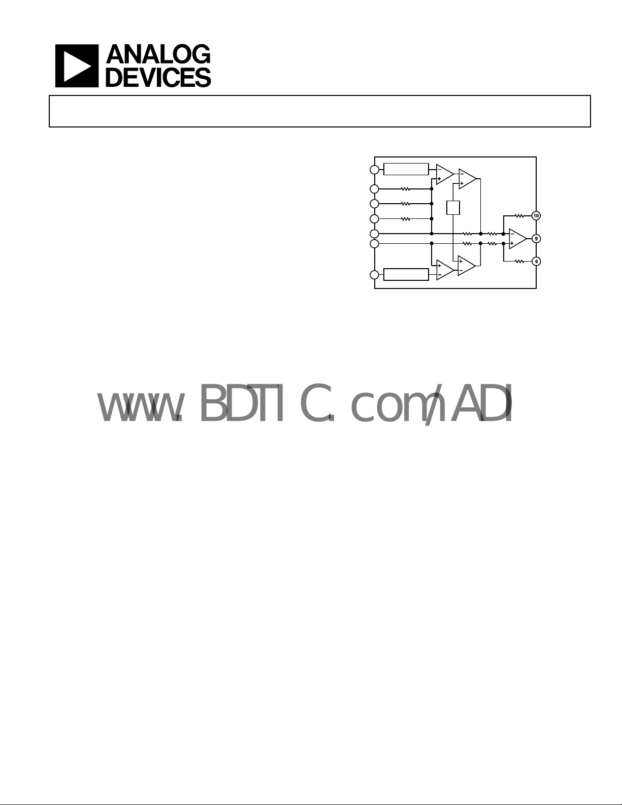
FUNCTIONAL BLOCK DIAGRAM
PROTECTION
1
– INPUT
G = 10
G = 100
G = 1000
RG
RG
+ INPUT
1
2
12
11
16
3
2
PROTECTION
404Ω
40Ω
V
b
20kΩ
20kΩ
Figure 1.
4.44kΩ
13
higher linearity C grade are specified from −25°C to +85°C.
The S grade guarantees performance to specification over the
extended temperature range −55°C to +125°C. The AD524 is
available in a 16-lead ceramic DIP, 16-lead SBDIP, 16-lead SOIC
wide packages, and 20-terminal leadless chip carrier.
PRODUCT HIGHLIGHTS
1. The AD524 has guaranteed low offset voltage, offset
voltage drift, and low noise for precision high gain
applications.
2. The AD524 is functionally complete with pin program-
mable gains of 1, 10, 100, and 1000, and single resistor
programmable for any gain.
3. Input and output offset nulling terminals are provided for
very high precision applications and to minimize offset
voltage changes in gain ranging applications.
4. The AD524 is input protected for both power-on and
power-off fault conditions.
5. The AD524 offers superior dynamic performance with a
gain bandwidth product of 25 MHz, full power response of
75 kHz and a settling time of 15 μs to 0.01% of a 20 V step
(G = 100).
20kΩ
20kΩ
AD524
20kΩ
20kΩ
SENSE
OUTPUT
REFERENCE
00500-001
Rev. F
Information furnished by Analog Devices is believed to be accurate and reliable. However, no
responsibility is assumed by Anal og Devices for its use, nor for any infringements of patents or ot her
rights of third parties that may result from its use. Specifications subject to change without notice. No
license is granted by implication or otherwise under any patent or patent rights of Analog Devices.
Trademarks and registered trademarks are the property of their respective owners.
One Technology Way, P.O. Box 9106, Norwood, MA 02062-9106, U.S.A.
Tel: 781.329.4700 www.analog.com
Fax: 781.461.3113 ©2007 Analog Devices, Inc. All rights reserved.

AD524
www.BDTIC.com/ADI
TABLE OF CONTENTS
Features .............................................................................................. 1
Functional Block Diagram .............................................................. 1
General Description ......................................................................... 1
Product Highlights ........................................................................... 1
Revision History ............................................................................... 2
Specifications ..................................................................................... 3
Absolute Maximum Ratings ............................................................ 8
Connection Diagrams .................................................................. 8
ESD Caution .................................................................................. 8
Typical Performance Characteristics ............................................. 9
Test Circuits ................................................................................. 14
Theory of Operation ...................................................................... 15
Input Protection .......................................................................... 15
REVISION HISTORY
11/07—Rev. E to Rev. F
Updated Format .................................................................. Universal
Changes to General Description .................................................... 1
Changes to Figure 1 .......................................................................... 1
Changes to Figure 3 and Figure 4 Captions .................................. 8
Changes to Error Budget Analysis Section ................................. 21
Changes to Ordering Guide .......................................................... 25
4/99—Rev. D to Rev. E
Input Offset and Output Offset ................................................ 15
Gain .............................................................................................. 16
Input Bias Currents .................................................................... 17
Common-Mode Rejection ........................................................ 17
Grounding ................................................................................... 18
Sense Terminal ............................................................................ 18
Reference Terminal .................................................................... 18
Programmable Gain ................................................................... 20
Autozero Circuits ....................................................................... 20
Error Budget Analysis ................................................................ 21
Outline Dimensions ....................................................................... 24
Ordering Guide .......................................................................... 25
Rev. F | Page 2 of 28
AD524
www.BDTIC.com/ADI
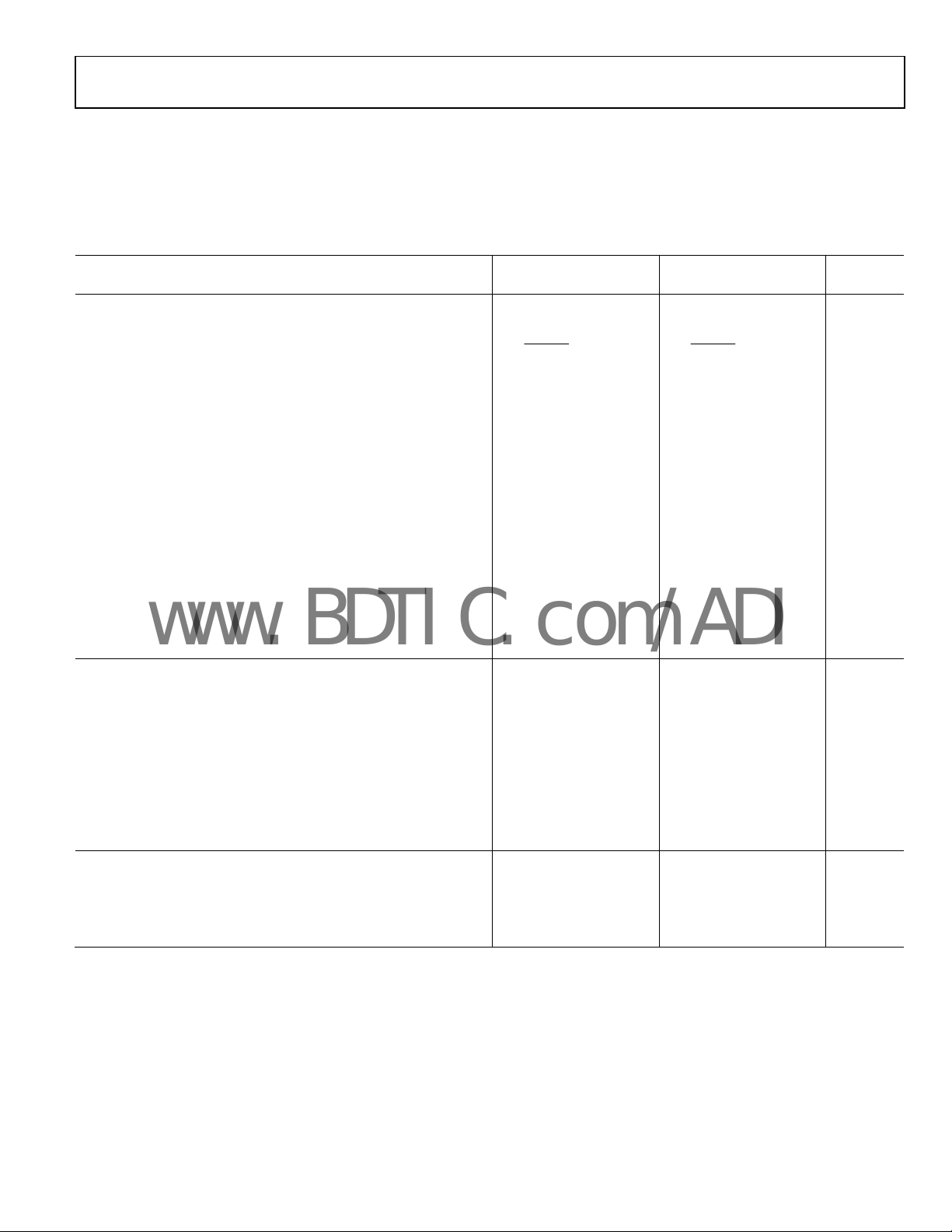
SPECIFICATIONS
@ VS = ±15 V, RL = 2 kΩ and TA = +25°C, unless otherwise noted.
All min and max specifications are guaranteed. Specifications shown in boldface are tested on all production units at the final electrical
test. Results from those tests are used to calculate outgoing quality levels.
Table 1.
AD524A AD524B
Parameter Min Typ Max Min Typ Max Unit
GAIN
Gain Equation (External Resistor Gain Programming)
Gain Range (Pin Programmable) 1 to 1000 1 to 1000
Gain Error
Nonlinearity
Gain vs. Temperature
VOLTAGE OFFSET (May be Nulled)
Input Offset Voltage
Output Offset Voltage 5
Offset Referred to the Input vs. Supply
INPUT CURRENT
Input Bias Current
Input Offset Current
1
G = 1
G = 10
G = 100
G = 1000
G = 1 ±0.01 ±0.005 %
G = 10, G = 100 ±0.01 ±0.005 %
G = 1000 ±0.01 ±0.01 %
G = 1 5 5 ppm/°C
G = 10 15 10 ppm/°C
G = 100 35 25 ppm/°C
G = 1000 100 50 ppm/°C
vs. Temperature 2
vs. Temperature 100
G = 1
G = 10
G = 100
G = 1000
vs. Temperature ±100 ±100 pA/°C
vs. Temperature ±100 ±100 pA/°C
70
85
95
100
⎡
⎢
R
⎣
⎤
000,40
+
G
±
⎥
⎦
%201
±0.05
±0.25
±0.5
±2.0
250
±50
±35
⎡
⎢
⎣
75
95
105
110
⎤
000,40
+
R
⎥
G
⎦
dB
dB
dB
dB
±
±0.03
±0.15
±0.35
±1.0
100
0.75
3
50
±25
±15
%201
%
%
%
%
μV
μV/°C
mV
μV
nA
nA
Rev. F | Page 3 of 28
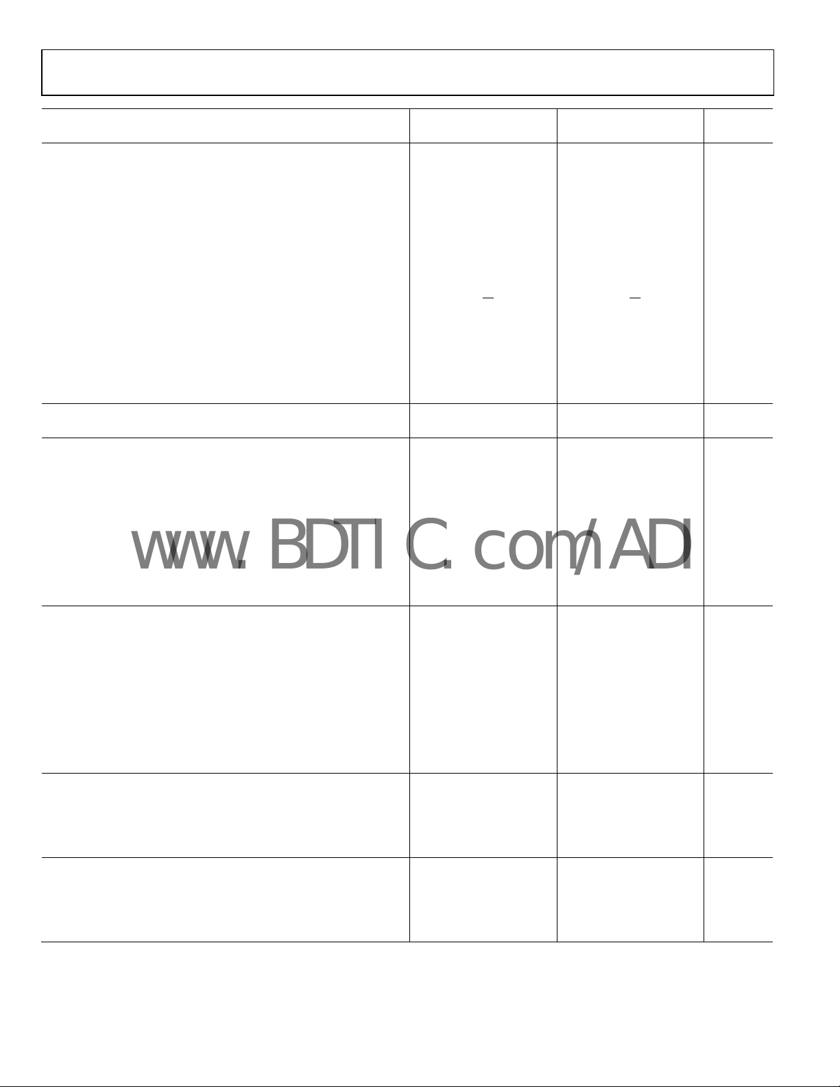
AD524
www.BDTIC.com/ADI
AD524A AD524B
Parameter Min Typ Max Min Typ Max Unit
INPUT
Input Impedance
Differential Resistance 109 109 Ω
Differential Capacitance 10 10 pF
Common-Mode Resistance 109 109 Ω
Common-Mode Capacitance 10 10 pF
Input Voltage Range
Maximum Differential Input Linear (VDL)
Maximum Common-Mode Linear (VCM)
Common-Mode Rejection DC to 60 Hz with 1 kΩ Source Imbalance V
G = 1
G = 10
G = 100
G = 1000
OUTPUT RATING
V
, RL = 2 kΩ ±10 ±10 V
OUT
DYNAMIC RESPONSE
Small Signal – 3 dB
G = 1 1 1 MHz
G = 10 400 400 kHz
G = 100 150 150 kHz
G = 1000 25 25 kHz
Slew Rate 5.0 5.0 V/μs
Settling Time to 0.01%, 20 V Step
G = 1 to 100 15 15 μs
G = 1000 75 75 μs
NOISE
Voltage Noise, 1 kHz
RTI 7 7 nV/√Hz
RTO 90 90 nV√Hz
RTI, 0.1 Hz to 10 Hz
G = 1 15 15 μV p-p
G = 10 2 2 μV p-p
G = 100, 1000 0.3 0.3 μV p-p
Current Noise
0.1 Hz to 10 Hz 60 60 pA p-p
SENSE INPUT
RIN 20 20 kΩ ± 20%
IIN 15 15 μA
Voltage Range ±10 ±10 V
Gain to Output 1 1 %
REFERENCE INPUT
RIN 40 40 kΩ ± 20%
IIN 15 15 μA
Voltage Range ±10 ±10 V
Gain to Output 1 1 %
2
±10 ±10 V
2
70
90
100
110
G
⎛
V12
⎜
⎝
⎞
×−
V
⎟
D
2
⎠
G
75
95
105
115
⎛
V12
⎜
⎝
dB
dB
dB
dB
⎞
×−
V
⎟
D
2
⎠
V
Rev. F | Page 4 of 28
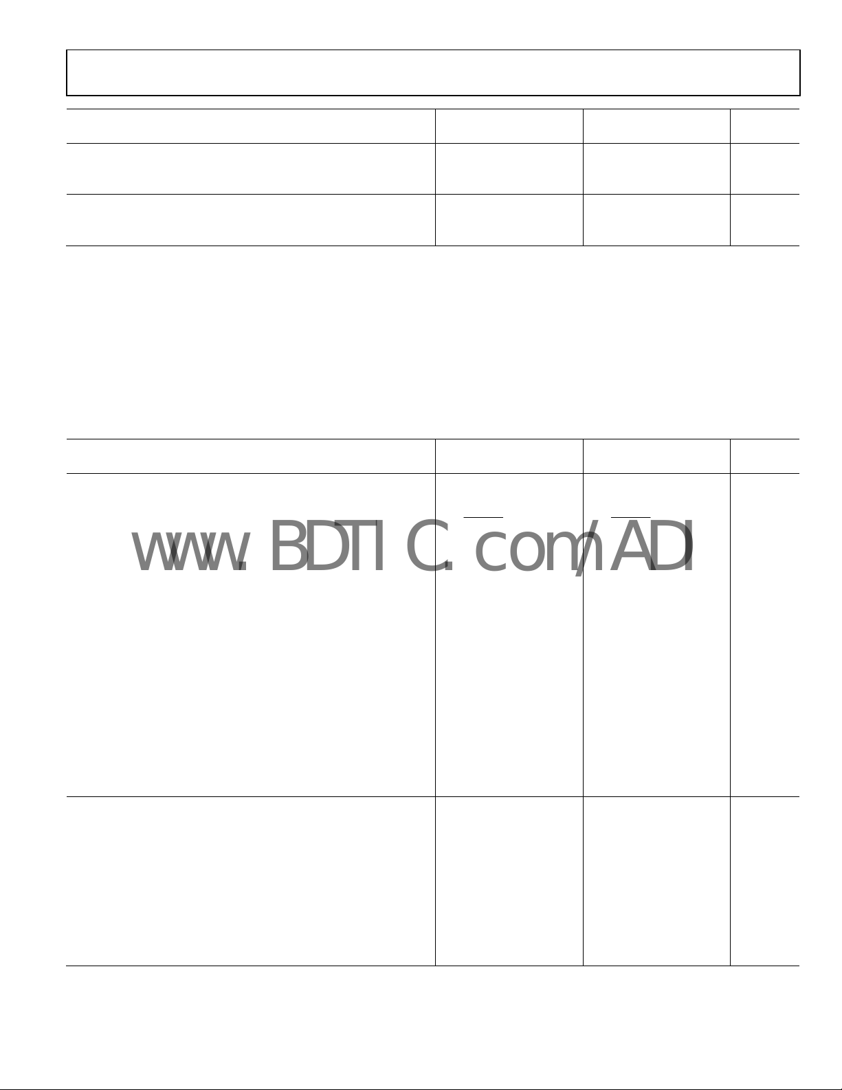
AD524
www.BDTIC.com/ADI
AD524A AD524B
Parameter Min Typ Max Min Typ Max Unit
TEMPERATURE RANGE
Specified Performance –25 +85 –25 +85 °C
Storage –65 +150 –65 +150 °C
POWER SUPPLY
Power Supply Range
Quiescent Current 3.5
1
Does not include effects of external resistor, RG.
2
VOL is the maximum differential input voltage at G = 1 for specified nonlinearity.
VDL at the maximum = 10 V/G.
VD = actual differential input voltage.
Example: G = 10, V
V
= 12 V − (10/2 × 0.50 V) = 9.5 V.
CM
= 0.50.
D
±6
@ V
= ±15 V, RL = 2 kΩ and TA = +25°C, unless otherwise noted.
S
All min and max specifications are guaranteed. Specifications shown in boldface are tested on all production units at the final electrical
test. Results from those tests are used to calculate outgoing quality levels.
Table 2.
AD524C AD524S
Parameter Min Typ Max Min Typ Max Unit
GAIN
Gain Equation (External Resistor Gain Programming)
Gain Range (Pin Programmable) 1 to 1000 1 to 1000
Gain Error
Nonlinearity
Gain vs. Temperature
VOLTAGE OFFSET (May be Nulled)
Input Offset Voltage
Output Offset Voltage
Offset Referred to the Input vs. Supply
1
G = 1
G = 10
G = 100
G = 1000
G = 1 ±0.003 ±0.01 %
G = 10, G = 100 ±0.003 ±0.01 %
G = 1000 ±0.01 ±0.01 %
G = 1 5 5 ppm/°C
G = 10 10 10 ppm/°C
G = 100 25 25 ppm/°C
G = 1000 50 50 ppm/°C
vs. Temperature
vs. Temperature
G = 1
G = 10
G = 100
G = 1000
80
100
110
115
±15
⎡
000,40
⎢
⎣
+
R
G
±18 ±6
5.0
⎤
±
⎥
3.5
%201
⎦
±0.02
±0.1
±0.25
±0.5
50
0.5
2.0
25
75
95
105
110
±15
⎡
000,40
⎢
R
G
⎣
dB
dB
dB
dB
±18
5.0
⎤
+
⎥
%201
±
⎦
±0.05
±0.25
±0.5
±2.0
100
2.0
3.0
50
V
mA
%
%
%
%
μV
μV/°C
mV
μV
Rev. F | Page 5 of 28
AD524
www.BDTIC.com/ADI
AD524C AD524S
Parameter Min Typ Max Min Typ Max Unit
INPUT CURRENT
Input Bias Current
vs. Temperature ±100 ±100 pA/°C
Input Offset Current
vs. Temperature ±100 ±100 pA/°C
INPUT
Input Impedance
Differential Resistance 109 109 Ω
Differential Capacitance 10 10 pF
Common-Mode Resistance 109 109 Ω
Common-Mode Capacitance 10 10 pF
Input Voltage Range
Maximum Differential Input Linear (VDL)
Maximum Common-Mode Linear (VCM)
2
±10 ±10 V
2
V12
Common-Mode Rejection DC to 60 Hz with 1 kΩ Source Imbalance V
G = 1
G = 10
G = 100
G = 1000
OUTPUT RATING
V
, RL = 2 kΩ ±10 ±10 V
OUT
DYNAMIC RESPONSE
Small Signal – 3 dB
G = 1 1 1 MHz
G = 10 400 400 kHz
G = 100 150 150 kHz
G = 1000 25 25 kHz
Slew Rate 5.0 5.0 V/μs
Settling Time to 0.01%, 20 V Step
G = 1 to 100 15 15 μs
G = 1000 75 75 μs
NOISE
Voltage Noise, 1 kHz
RTI 7 7 nV/√Hz
RTO 90 90 nV√Hz
RTI, 0.1 Hz to 10 Hz
G = 1 15 15 μV p-p
G = 10 2 2 μV p-p
G = 100, 1000 0.3 0.3 μV p-p
Current Noise
0.1 Hz to 10 Hz 60 60 pA p-p
SENSE INPUT
RIN 20 20 kΩ ± 20%
IIN 15 15 μA
Voltage Range ±10 ±10 V
Gain to Output 1 1 %
80
100
110
120
±15
±10
G
⎛
⎜
⎝
⎞
V
×−
⎟
D
2
⎠
70
90
100
110
±50
±35
G
⎛
V12
⎜
⎝
dB
dB
dB
dB
⎞
V
×−
⎟
D
2
⎠
nA
nA
V
Rev. F | Page 6 of 28

AD524
www.BDTIC.com/ADI
AD524C AD524S
Parameter Min Typ Max Min Typ Max Unit
REFERENCE INPUT
RIN 40 40 kΩ ± 20%
IIN 15 15 μA
Voltage Range 10 10 V
Gain to Output 1 1 %
TEMPERATURE RANGE
Specified Performance –25 +85 –55 +85 °C
Storage –65 +150 –65 +150 °C
POWER SUPPLY
Power Supply Range
Quiescent Current 3.5
1
Does not include effects of external resistor RG.
2
VOL is the maximum differential input voltage at G = 1 for specified nonlinearity.
V
at the maximum = 10 V/G.
DL
VD = actual differential input voltage.
Example: G = 10, VD = 0.50.
VCM = 12 V − (10/2 × 0.50 V) = 9.5 V.
±6
±15
±18 ±6
5.0
3.5
±15
±18
5.0
V
mA
Rev. F | Page 7 of 28
AD524
O
O
www.BDTIC.com/ADI
ABSOLUTE MAXIMUM RATINGS
Table 3.
Parameter Rating
Supply Voltage ±18 V
Internal Power Dissipation 450 mW
Input Voltage1
(Either Input Simultaneously) |VIN| + |VS| <36 V
Output Short-Circuit Duration Indefinite
Storage Temperature Range
(R) –65°C to +125°C
(D, E) –65°C to +150°C
Operating Temperature Range
AD524A/AD524B/AD524C –25°C to +85°C
AD524S –55°C to +125°C
Lead Temperature (Soldering, 60 sec) +300°C
1
Maximum input voltage specification refers to maximum voltage to which
either input terminal may be raised with or without device power applied.
For example, with ±18 volt supplies maximum, VIN is ±18 V; with zero supply
voltage maximum, VIN is ±36 V.
Stresses above those listed under Absolute Maximum Ratings
may cause permanent damage to the device. This is a stress
rating only; functional operation of the device at these or any
other conditions above those indicated in the operational
section of this specification is not implied. Exposure to absolute
maximum rating conditions for extended periods may affect
device reliability.
OUTPUT
UTPUT
NULL
RG116
–INPUT
+INPUT
RG
G = 10
NULL
15
1
2
2
3
13
14
4
INPUT
NULL
PAD NUMBERS CORRESPOND TO PIN NUMBERS FOR
THE D-16 AND RW-16 16-L EAD CERAMIC PACKAGES.
G = 100
12
5
INPUT
NULL
G = 1000
11
0.170 (4.33)
SENSE
10
REFERENCE
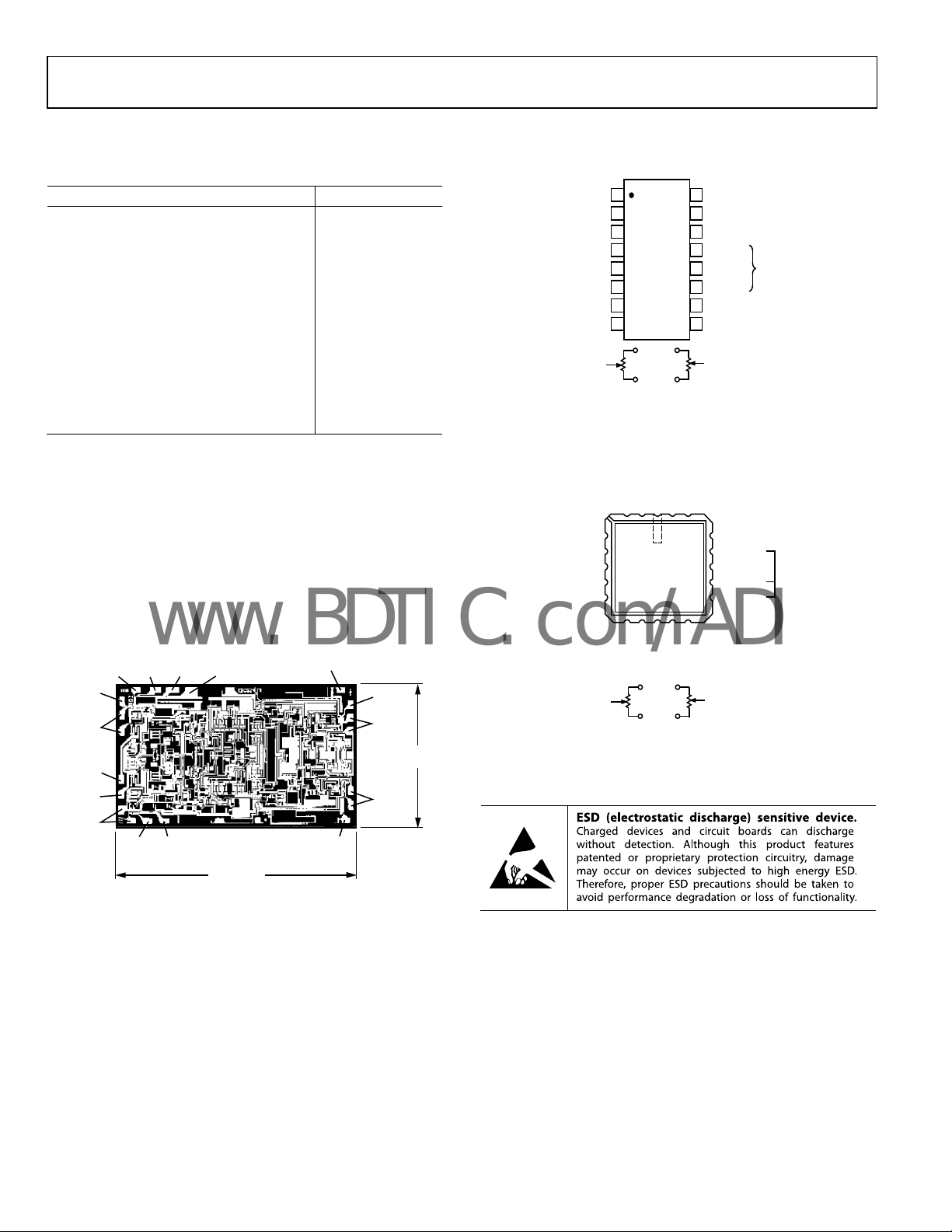
Figure 2. Metallization Photograph
Contact factory for latest dimensions;
Dimensions shown in inches and (mm)
9
OUTPUT
8 +V
S
0.103
(2.61)
7 –V
S
6
00500-002
NC = NO CONNECT
ESD CAUTION
CONNECTION DIAGRAMS
1
– INPUT
2
+ INPUT
RG
3
2
AD524
INPUT NULL
INPUT NULL
REFERENCE
OFFSET NULL
INPUT NULL
INPUT NULL
REFERENCE
OFFSET NULL
4
TOP VIEW
5
(Not to Scale)
6
–V
7
S
+V
8
S
+V
INPUT
415
S
514
Figure 3. Ceramic (D) and
SOIC (RW-16 and D-16) Packages
1
RG
–INPUT3+INPUT
20
1NC2
4
RG
2
5
AD524
6
NC
7
8
+V
INPUT
S
TOP VIEW
(Not to Scal e)
11NC10
9
S
S
–V
+V
719
518
12
OUTPUT
Figure 4. Leadless Chip Carrier (E)
16
RG
1
15
OUTPUT NULL
14
OUTPUT NULL
13
G = 10
12
G = 100
11
G = 1000
10
SENSE
9
OUTPUT
–V
S
OUTPUT
OFFSET NULL
OUTPUT
NULL
19
18
OUTPUT NULL
17
G = 10
16
NC
15
G = 100
14
G = 1000
13
SENSE
–V
S
OUTPUT
OFFSET NULL
SHORT TO
RG
FOR
2
DESIRED
GAIN
SHORT T
RG2 FOR
DESIRED
GAIN
0500-003
00500-004
Rev. F | Page 8 of 28
AD524
www.BDTIC.com/ADI
TYPICAL PERFORMANCE CHARACTERISTICS
20
15
10
+25°C
INPUT VOLTAGE (±V)
5
0
0 5 10 15 20
SUPPLY VOLTAGE (±V)
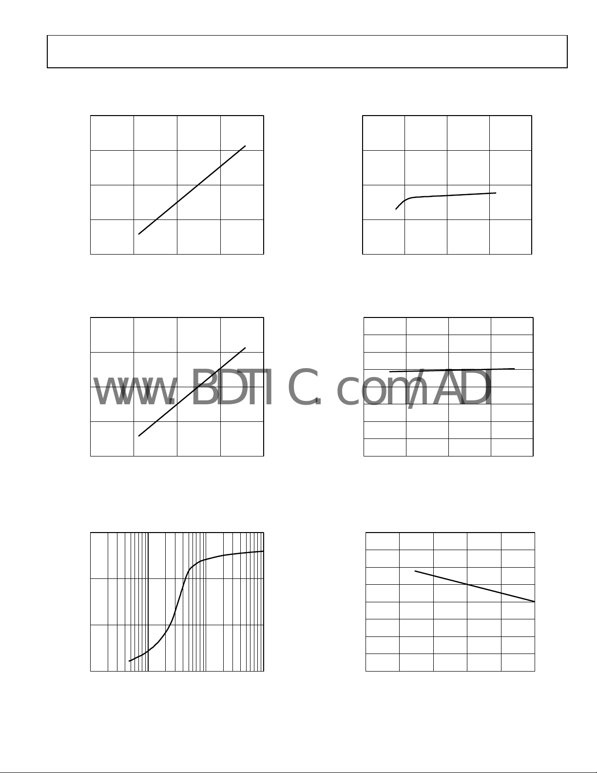
Figure 5. Input Voltage Range vs. Supply Voltage, G = 1
20
15
10
8
6
4
2
QUIESCE NT CURRENT (mA)
00500-005
0
0 5 10 15 20
SUPPLY VOLTAGE (±V)
00500-008
Figure 8. Quiescent Current vs. Supply Voltage
16
14
12
10
8
5
OUTPUT VOLTAGE SWING (±V)
0
0 5 10 15 20
SUPPLY VOLTAGE (±V)
Figure 6. Output Voltage Swing vs. Supply Voltage
30
20
10
OUTPUT VOLTAGE SWING (V p-p)
0
10 100 1k 10k
LOAD RESI STANCE (Ω)
Figure 7. Output Voltage Swing vs. Load Resistance
6
4
INPUT BI AS CURRENT (±n A)
2
00500-006
0
0 5 10 15 20
SUPPLY VOLTAG E (±V)
00500-009
Figure 9. Input Bias Current vs. Supply Voltage
40
30
20
10
0
–10
–20
INPUT BIAS CURRENT (n A)
–30
00500-007
–40
–75 –25 25 75 125
TEMPERATURE (°C)
00500-010
Figure 10. Input Bias Current vs. Temperature
Rev. F | Page 9 of 28

AD524
–
www.BDTIC.com/ADI
16
14
12
10
8
6
4
INPUT BIA S CURRENT (±n A)
2
0
0 5 10 15 20
INPUT VOLTAGE (±V)
Figure 11. Input Bias Current vs. Input Voltage
0
1
2
3
4
FROM FINAL VALUE (µV)
OS
5
ΔV
6
02461357
WARM-UP TIME (Minutes)
Figure 12. Offset Voltage, RTI, Turn-On Drift
00500-011
00500-012
8
140
G = 1000
G = 100
–120
G = 10
–100
G = 1
–80
–60
CMRR (dB)
–40
–20
0
0 100 10k 1M10 1k 100k 10M
FREQUENCY (Hz)
Figure 14. CMRR vs. Frequency, RTI, Zero to 1000 Source Imbalance
30
G = 1, 10, 100
20
10
FULL POWER RESPONSE (V p-p )
0
1k 10k 100k 1M
G = 1000 G = 100 G = 10
BANDWIDTH L IMIT ED
FREQUENCY ( Hz)
Figure 15. Large Signal Frequency Response
00500-014
00500-015
10
8
1000
100
10
GAIN (V/V)
1
0 100 10k 1M10 1k 100k 10M
FREQUENCY (Hz)
Figure 13. Gain vs. Frequency
00500-013
6
4
SLEW RATE (V/µs)
2
0
1 10 100 1000
Figure 16. Slew Rate vs. Gain
Rev. F | Page 10 of 28
G = 1000
00500-016
GAIN (V/V)

AD524
www.BDTIC.com/ADI
160
140
120
100
80
60
40
20
POWER SUPPLY REJECTI ON RATIO (dB)
0
100 10k10 1k 100k
FREQUENCY (Hz)
+VS = 15V DC +
1V p-p SINEWAVE
G
=
1
0
0
0
G
=
1
0
0
G
=
1
0
G
=
1
00500-017
Figure 17. Positive PSRR vs. Frequency
160
140
120
100
80
60
40
–VS = –15V DC +
1V p-p SINEWAVE
G
=
1
0
0
0
G
=
1
0
0
G
=
1
0
G
=
1
100k
10k
1k
100
CURRENT NOISE SPECTRAL DENSITY (fA/ Hz)
0 10k
1 10 100 1k
FREQUENCY (Hz)
Figure 20. Input Current Noise vs. Frequency
0.1Hz TO 10Hz
5mV 1s
00500-020
20
POWER SUPPLY REJECTI ON RATIO (dB)
0
100 10k10 1k 100k
FREQUENCY (Hz)
Figure 18. Negative PSRR vs. Frequency
1000
100
10
VOLT NSD (nV/ Hz)
1
0.1
1 100k
10 100 1k 10k
G = 1
G = 10
G = 100, 1000
FREQUENCY (Hz)
Figure 19. RTI Noise Spectral Density vs. Gain
G = 1000
00500-018
VERTICAL SCALE; 1 DI VISIO N = 5µV
00500-021
Figure 21. Low Frequency Noise, G = 1 (System Gain = 1000)
0.1Hz TO 10Hz
10mV 1s
00500-019
VERTICAL SCALE; 1 DIVISION = 0.1µV
00500-022
Figure 22. Low Frequency Noise, G = 1000 (System Gain = 100,000)
Rev. F | Page 11 of 28

AD524
–
www.BDTIC.com/ADI
–12 TO +12
–8 TO +8
–4 TO +4
OUTPUT
STEP (V)
+4 TO –4
1% 0.1% 0. 01%
1mV 10V 10µs
+8 TO –8
1% 0.1% 0.01%
+12 TO –12
0 5 10 15 20
SETTLING TIME (µs)
Figure 23. Settling Time, Gain = 1
10V 10µs1mV
Figure 24. Large Signal Pulse Response and Settling Time, Gain =1
00500-023
0500-026
Figure 26. Large Signal Pulse Response and Settling Time, Gain = 10
12 TO +12
–8 TO +8
–4 TO +4
OUTPUT
STEP (V)
+4 TO –4
+8 TO –8
+12 TO –12
0 5 10 15 20
00500-024
0.1%
1%
1%
0.1%
SETTLING TIME (µs)
0.01%
0.01%
00500-027
Figure 27. Settling Time, Gain = 100
–12 TO +12
–8 TO +8
–4 TO +4
OUTPUT
STEP (V)
+4 TO –4
+8 TO –8
+12 TO –12
1%
1% 0.1%
0 5 10 15 20
0.1%
SETTLING TIME (µs)
Figure 25. Settling Time, Gain = 10
0.01%
1mV 10V 10µs
0.01%
00500-025
Figure 28. Large Signal Pulse Response and Settling Time, Gain = 100
Rev. F | Page 12 of 28
0500-028

AD524
www.BDTIC.com/ADI
–12 TO +12
–8 TO +8
–4 TO +4
OUTPUT
STEP (V)
+4 TO –4
+8 TO –8
+12 TO –12
1% 0.01%
1% 0.01%
0 102030405060708
SETTLING TIME (µs)
Figure 29. Settling Time, Gain = 1000
0.1%
0.1%
00500-029
0
5mV 10V 20µs
0500-030
Figure 30. Large Signal Pulse Response and Settling Time, Gain = 1000
Rev. F | Page 13 of 28

AD524
www.BDTIC.com/ADI
TEST CIRCUITS
10kΩ
1kΩ
0.01%
INPUT
20V p-p
11kΩ
0.1%
100kΩ
0.1%
1kΩ
0.1%
100Ω
0.1%
RG
G = 10
G = 100
G = 1000
RG
1
2
+V
1
–
8
16
13
12
AD524
11
3
7
2
+
–V
Figure 31. Settling Time Test Circuit
+V
S
10kΩ
10T
0.1%
V
S
10
6
S
OUT
9
00500-031
V
B
R56
20kΩ
S
50µA
C4C3
RG
G = 100
G = 1000
I
2
Q2, Q4
2
I
4
50µA
–IN
CH
CH
CH2,
3
1
, CH
I
1
50µA
A1 A2
++
R57
20kΩ
4
Q1, Q3
4.44kΩ
RG
1
404Ω
I
50µA
3
40Ω
–V
Figure 32. Simplified Circuit of Amplifier; Gain Is Defined as
((R56 + R57)/(R
)) +1; For a Gain of 1, RG Is an Open Circuit
G
R53
20kΩ
R54
20kΩ
CH
, CH3,
2
CH
R52
20kΩ
SENSE
A3
V
O
R55
20kΩ
REFERENCE
4
CH
+IN
1
00500-032
Rev. F | Page 14 of 28

AD524
V
www.BDTIC.com/ADI
THEORY OF OPERATION
The AD524 is a monolithic instrumentation amplifier based
on the classic 3-op amp circuit. The advantage of monolithic
construction is the closely matched components that enhance
the performance of the input preamplifier. The preamplifier
section develops the programmed gain by the use of feedback
concepts. The programmed gain is developed by varying the
value of R
(smaller values increase the gain) while the feedback
G
forces the collector currents (Q1, Q2, Q3, and Q4) to be constant,
which impresses the input voltage across R
is reduced to increase the programmed gain, the
As R
G
.
G
transconductance of the input preamplifier increases to the
transconductance of the input transistors. This has three
important advantages. First, this approach allows the circuit
to achieve a very high open-loop gain of 3 × 10
8
at a programmed
gain of 1000, thus reducing gain-related errors to a negligible
30 ppm. Second, the gain bandwidth product, which is determined by C3 or C4 and the input transconductance, reaches
25 MHz. Third, the input voltage noise reduces to a value
determined by the collector current of the input transistors
for an RTI noise of 7 nV/√Hz at G = 1000.
INPUT PROTECTION
As interface amplifiers for data acquisition systems, instrumentation amplifiers are often subjected to input overloads,
that is, voltage levels in excess of the full scale for the selected
gain range. At low gains (10 or less), the gain resistor acts as a
current limiting element in series with the inputs. At high gains,
the lower value of R
does not adequately protect the inputs
G
+
–
AD524
+
S
8
10
9
6
7
–V
S
G = 1000
100
1000
RG
1
16
10
13
12
11
2
3
2
16.2kΩ
1µF
G = 1, 10, 100
100Ω
from excessive currents. Standard practice is to place series
limiting resistors in each input, but to limit input current to
below 5 mA with a full differential overload (36 V) requires
over 7k of resistance, which adds 10 nV√Hz of noise. To
provide both input protection and low noise, a special series
protection FET is used.
A unique FET design was used to provide a bidirectional
current limit, thereby protecting against both positive and
negative overloads. Under nonoverload conditions, three
channels (CH
, CH3, CH4) act as a resistance (≈1 kΩ) in series
2
with the input as before. During an overload in the positive
direction, a fourth channel, CH
, acts as a small resistance
1
(≈3 kΩ) in series with the gate, which draws only the leakage
current, and the FET limits I
. When the FET enhances under
DSS
a negative overload, the gate current must go through the small
FET formed by CH
and when this FET goes into saturation,
1
the gate current is limited and the main FET goes into controlled
enhancement. The bidirectional limiting holds the maximum
input current to 3 mA over the 36 V range.
INPUT OFFSET AND OUTPUT OFFSET
Voltage offset specifications are often considered a figure of
merit for instrumentation amplifiers. While initial offset may
be adjusted to zero, shifts in offset voltage due to temperature
variations causes errors. Intelligent systems can often correct
this factor with an autozero cycle, but there are many smallsignal high-gain applications that do not have this capability.
AD712
+V
s
3
+
8
1/2
–
2
1µF
1
9.09kΩ
1kΩ
5
6
1.62MΩ
+
1/2
–
7
4
1µF
–V
S
16.2kΩ
1.82kΩ
Figure 33. Noise Test Circuit
Rev. F | Page 15 of 28
0500-033

AD524
–
Ω
V
V
www.BDTIC.com/ADI
Voltage offset and drift comprise two components each; input
and output offset and offset drift. Input offset is the component
of offset that is directly proportional to gain, that is, input offset
as measured at the output at G = 100 is 100 times greater than at
G = 1. Output offset is independent of gain. At low gains, output
offset drift is dominant, at high gains, input offset drift dominates.
Therefore, the output offset voltage drift is normally specified as
drift at G = 1 (where input effects are insignificant), whereas
input offset voltage drift is given by drift specification at a high
gain (where output offset effects are negligible). All input
related numbers are referred to the input (RTI) that is the effect
on the output is G times larger. Voltage offset vs. power supply
is also specified at one or more gain settings and is also RTI.
By separating these errors, one can evaluate the total error
independent of the gain setting used. In a given gain configuration, both errors can be combined to give a total error referred
to the input (RTI) or output (RTO) by the following formulas:
Total error RTI = input error + (output error/gain)
Total error RTO = (gain × input error) + output error
As an illustration, a typical AD524 might have a +250 µV
output offset and a −50 µV input offset. In a unity gain
configuration, the total output offset would be 200 µV or
the sum of the two. At a gain of 100, the output offset would
be −4.75 mV or: +250 µV + 100(−50 µV) = −4.75 mV.
The AD524 provides for both input and output offset adjustment.
This simplifies very high precision applications and minimizes
offset voltage changes in switched gain applications. In such
applications, the input offset is adjusted first at the highest
programmed gain, then the output offset is adjusted at G = 1.
GAIN
The AD524 has internal high accuracy pretrimmed resistors
for pin programmable gains of 1, 10, 100, and 1000. One of the
preset gains can be selected by pin strapping the appropriate
gain terminal and RG
INPUT
G = 100
G = 1000
RG
+INPUT
Figure 34. Operating Connections for G = 100
together (for G = 1, RG2 is not connected).
2
10kΩ
4
AD524
7
–V
S
INPUT
OFFSET
NULL
5
10
9
6
RG
G = 10
2
+V
S
8
1
16
1
13
12
11
3
2
V
OUT
OUTPUT
SIGNAL
COMMON
00500-034
The AD524 can be configured for gains other than those that
are internally preset; there are two methods to do this. The first
method uses just an external resistor connected between
Pin 3 and Pin 16 (see Figure 35), which programs the gain
according to the following formula:
k40
=
R
G
For best results, R
temperature coefficient. An external R
1
−=
G
should be a precision resistor with a low
G
affects both gain
G
accuracy and gain drift due to the mismatch between it and
the internal thin-film resistors. Gain accuracy is determined
by the tolerance of the external R
and the absolute accuracy
G
of the internal resistors (±20%). Gain drift is determined by the
mismatch of the temperature coefficient of R
and the tempera-
G
ture coefficient of the internal resistors (−50 ppm/°C typical).
+
S
–INPUT
1.5kΩ
1kΩ
+INPUT
RG
2.105kΩ
RG
1
16
1
13
12
11
2
2
3
8
AD524
7
–V
10
9
6
40,000
G = + 1 = 20 ±20%
S
2.105
V
OUT
REFERENCE
Figure 35. Operating Connections for G = 20
The second method uses the internal resistors in parallel with
an external resistor (see Figure 36). This technique minimizes
the gain adjustment range and reduces the effects of temperature coefficient sensitivity.
+
S
–INPUT
RG
1
G = 10
4kΩ
RG
+INPUT
2
*R|
= 4444.44Ω
G = 10
*R|
= 404.04Ω
G = 100
*R|
= 40.04Ω
G = 1000
*NOMINAL (±20%)
Figure 36. Operating Connections for G = 20, Low Gain
1
3
2
8
AD524
7
–V
S
10
6
G =
4000||4444.44
9
40,000
16
13
12
11
Temperature Coefficient Technique
V
OUT
REFERENCE
+ 1 = 20 ±17%
00500-035
00500-036
Rev. F | Page 16 of 28

AD524
T
V
V
www.BDTIC.com/ADI
The AD524 can also be configured to provide gain in the output
stage. Figure 37 shows an H pad attenuator connected
to the reference and sense lines of the AD524. R1, R2, and R3
should be made as low as possible to minimize the gain variation
and reduction of CMRR. Varying R2 precisely sets the gain
without affecting CMRR. CMRR is determined by the match
of R1 and R3.
+V
–INPUT
+INPUT
(R2||40kΩ) + R1 + R3
G =
(R2||40kΩ)
G = 10
G = 100
G = 1000
RG
RG
1
16
1
13
12
11
3
2
2
8
AD524
7
–V
S
10
6
S
(R1 + R2 + R3)||RL ≥ 2kΩ
R1
2.26kΩ
R2
5kΩ
9
R3
2.26kΩ
V
OU
R
L
00500-037
Figure 37. Gain of 2000
Table 4. Output Gain Resistor Values
Output Gain R2 R1, R3 Nominal Gain
2 5 kΩ 2.26 kΩ 2.02
5 1.05 kΩ 2.05 kΩ 5.01
10 1 kΩ 4.42 kΩ 10.1
INPUT BIAS CURRENTS
Input bias currents are those currents necessary to bias the
input transistors of a dc amplifier. Bias currents are an
additional source of input error and must be considered in
a total error budget. The bias currents, when multiplied by
the source resistance, appear as an offset voltage. What is of
concern in calculating bias current errors is the change in bias
current with respect to signal voltage and temperature. Input
offset current is the difference between the two input bias
currents. The effect of offset current is an input offset voltage
whose magnitude is the offset current times the source
impedance imbalance.
+V
S
2
+
8
3
11
12
AD524
13
16
1
–
Figure 38. Indirect Ground Returns for Bias Currents—Transformer Coupled
2
+
3
11
AD524
12
13
16
1
–
Figure 39. Indirect Ground Returns for Bias Currents—Thermocouple
10
9
6
7
–V
S
+V
S
8
7
–V
S
LOAD
TO POWER
SUPPLY
GROUND
10
9
6
LOAD
TO POWER
SUPPLY
GROUND
00500-038
00500-039
Rev. F | Page 17 of 28
+
S
2
+
8
3
11
12
13
16
1
AD524
–
10
9
6
7
–V
S
LOAD
TO POWER
SUPPLY
GROUND
00500-040
Figure 40. Indirect Ground Returns for Bias Currents–AC-Coupled
Although instrumentation amplifiers have differential inputs,
there must be a return path for the bias currents. If this is not
provided, those currents charge stray capacitances, causing the
output to drift uncontrollably or to saturate. Therefore, when
amplifying floating input sources such as transformers and
thermocouples, as well as ac-coupled sources, there must still
be a dc path from each input to ground.
COMMON-MODE REJECTION
Common-mode rejection is a measure of the change in output
voltage when both inputs are changed equal amounts. These
specifications are usually given for a full-range input voltage
change and a specified source imbalance. Common-mode
rejection ratio (CMRR) is a ratio expression whereas commonmode rejection (CMR) is the logarithm of that ratio. For
example, a CMRR of 10,000 corresponds to a CMR of 80 dB.
In an instrumentation amplifier, ac common-mode rejection is
only as good as the differential phase shift. Degradation of ac
common-mode rejection is caused by unequal drops across
differing track resistances and a differential phase shift due
to varied stray capacitances or cable capacitances. In many
applications, shielded cables are used to minimize noise. This
technique can create common-mode rejection errors unless the
shield is properly driven. Figure 41 and Figure 42 show active
data guards that are configured to improve ac common-mode
rejection by bootstrapping the capacitances of the input cabling,
thus minimizing differential phase shift.
+
–
+
1
1
16
12
3
2
2
8
AD524
7
–V
–
AD524
+
S
10
9
V
10
6
OUT
REFERENCE
9
V
OUT
REFERENCE
6
S
+V
S
8
7
–V
S
100Ω
100Ω
100Ω
–INPUT
1
G = 100
12
RG
2
AD711
+INPUT
3
2
Figure 41. Shield Driver, G ≥ 100
–INPUT
–V
S
+INPUT
RG
RG
AD712
Figure 42. Differential Shield Driver
00500-041
00500-042

AD524
V
www.BDTIC.com/ADI
GROUNDING
Many data acquisition components have two or more ground
pins that are not connected together within the device. These
grounds must be tied together at one point, usually at the system
power-supply ground. Ideally, a single solid ground would be
desirable. However, because current flows through the ground
wires and etch stripes of the circuit cards, and because these
paths have resistance and inductance, hundreds of millivolts can
be generated between the system ground point and the data
acquisition components. Separate ground returns should be
provided to minimize the current flow in the path from the
sensitive points to the system ground point. In this way, supply
currents and logic-gate return currents are not summed into the
same return path as analog signals where they would cause
measurement errors.
Because the output voltage is developed with respect to the
potential on the reference terminal, an instrumentation
amplifier can solve many grounding problems.
DIG
COM
DIGITAL P.S.
+5V
C–15V
7 9 11 15
AD574A
SIGNAL
GROUND
1µF1µF 1µF
1
DIGITAL
DATA
OUTPUT
2
AD524
1
OUTPUT
REFERENCE
ANALOG P.S.
C+15V
0.1
9
ANALOG
GROUND*
0.1
µF
µF
AD583
SAMPLE
AND HOLD
0.1
0.1
µF
µF
8
7
10
6
*IF INDE PENDENT; OTHERW ISE, RE TURN AMPL IFIE R REFERENCE
TO MECCA AT ANALOG P.S. COMMON.
Figure 43. Basic Grounding Practice
00500-043
SENSE TERMINAL
The sense terminal is the feedback point for the instrument
amplifier’s output amplifier. Normally, it is connected to the
instrument amplifier output. If heavy load currents are to be
drawn through long leads, voltage drops due to current flowing
through lead resistance can cause errors. The sense terminal can
be wired to the instrument amplifier at the load, thus putting
the IxR drops inside the loop and virtually eliminating this
error source.
+
(SENSE)
OUTPUT
(REF)
9
CURRENT
BOOSTE R
X1
R
L
00500-044
VIN+
V
8
2
3
12
–
1
IN
AD524
7
V–
10
6
Figure 44. AD524 Instrumentation Amplifier with Output Current Booster
Typically, IC instrumentation amplifiers are rated for a full
±10 volt output swing into 2 kΩ. In some applications, however,
the need exists to drive more current into heavier loads.
Figure 44 shows how a high current booster may be connected
inside the loop of an instrumentation amplifier to provide the
required current boost without significantly degrading overall
performance. Nonlinearities and offset and gain inaccuracies of
the buffer are minimized by the loop gain of the AD524 output
amplifier. Offset drift of the buffer is similarly reduced.
REFERENCE TERMINAL
The reference terminal can be used to offset the output by up to
±10 V. This is useful when the load is floating or does not share
a ground with the rest of the system. It also provides a direct
means of injecting a precise offset. It must be remembered that
the total output swing is ±10 V to be shared between signal and
reference offset.
When the AD524 is of the 3-amplifier configuration it
is necessary that nearly zero impedance be presented to the
reference terminal.
Any significant resistance from the reference terminal to
ground increases the gain of the noninverting signal path,
thereby upsetting the common-mode rejection of the AD524.
In the AD524, a reference source resistance unbalances the CMR
trim by the ratio of 20 kΩ/R
source impedance is 1 Ω, CMR is reduced to 86 dB (20 kΩ/1 Ω
= 86 dB). An operational amplifier can be used to provide that
low impedance reference point, as shown in Figure 45. The
input offset voltage characteristics of that amplifier adds directly
to the output offset voltage performance of the instrumentation
amplifier.
. For example, if the reference
REF
Rev. F | Page 18 of 28

AD524
www.BDTIC.com/ADI
VIN+
V
–
IN
2
3
12
1
+V
8
AD524
7
–V
S
S
SENSE
10
6
REF
AD711
9
LOAD
V
OFFSET
0500-045
Figure 45. Use of Reference Terminal to Provide Output Offset
An instrumentation amplifier can be turned into a voltageto-current converter by taking advantage of the sense and
reference terminals, as shown in Figure 46.
–IN
+IN
–V
+V
ANALOG
COMMON
INPUT
OFFSET
TRIM
S
S
1µF
35V
C2
C1
GAIN TABLE
ABGAIN
0
0
1
0
0
1
1
1
1
2
3
4
R1
10kΩ
5
6
7
8
K1 – K3 =
THERMOSEN DM2C
4.5V COIL
D1 – D3 = IN4148
10
1000
100
1
PROTECTION
PROTECTION
20kΩ
20kΩ
20kΩ
+V
S
20kΩ
20kΩ
20kΩ
A1
AD524
INPUTS
GAIN
RANGE
Figure 47. Three-Decade Gain Programmable Amplifier
16
15
14
4.44kΩ
13
404Ω
12
40Ω
11
10
9
1
A
B
2
3
4
5
6
+5V
7
NC = NO CONNECT
+INPUT
–INPUT
2
3
13
1
+
AD524
–
10
6
SENSE
REF
R1
9
V
A2
I
L
X
AD711
I
L
VXV
R1
40,000
IN
(
1 +
===
R1
)
R
G
LOAD
Figure 46. Voltage-to-Current Converter
By establishing a reference at the low side of a current setting
resistor, an output current may be defined as a function of input
voltage, gain, and the value of that resistor. Because only a small
current is demanded at the input of the buffer amplifier (A2)
the forced current, I
, largely flows through the load. Offset and
L
drift specifications of A2 must be added to the output offset and
drift specifications of the AD524.
OUTPUT
OFFSET
TRIM
R2
10kΩ
OUT
74LS138
DECODER
RELAY
SHIELDS
16
Y0
15
Y1
14
Y2
13
G = 10
K1
NC
K1 K2 K3D1 D2 D3
G = 100
K2
1
2
3
4
5
6
7
G = 1000
7407N
BUFFER
DRIVER
K3
+5V
16
10µF
LOGIC
COMMON
00500-046
00500-047
Rev. F | Page 19 of 28

AD524
+
www.BDTIC.com/ADI
PROGRAMMABLE GAIN
Figure 47 shows the AD524 being used as a software programmable gain amplifier. Gain switching can be accomplished with
mechanical switches such as DIP switches or reed relays. It should
be noted that the on resistance of the switch in series with the
internal gain resistor becomes part of the gain equation and has
an effect on gain accuracy.
The AD524 can also be connected for gain in the output stage.
Figure 48 shows an AD711 used as an active attenuator in the
output amplifier’s feedback loop. The active attenuation presents
very low impedance to the feedback resistors, therefore
minimizing the common-mode rejection ratio degradation.
(+INPUT)
–IN
(–INPUT)
+IN
INPUT
OFFSET
NULL
–V
S
V
S
1µF
35V
10kΩ
AD711
1
PROTECTION
2
PROTECTION
3
4
20kΩ
5
20kΩ
6
7
AD524
8
10pF
+V
S
–
+
–V
S
20kΩ
+
+V
20kΩ
15
13
11
9
S
–
20kΩ
20kΩ
20kΩ
VSSV
DD
18
AD7590
34567
V
DD
Figure 48. Programmable Output Gain
4.44kΩ
404Ω
40Ω
GND
16
A4A3A2 WR
16
OUTPUT
OFFSET
15
NULL
TO –V
R2
14
10kΩ
13
12
11
10
9
2
39.2kΩ
14
28.7kΩ
12
316kΩ
10
V
OUT
1kΩ
1kΩ
1kΩ
00500-048
+INPUT
(–INPUT)
G = 10
G = 100
G = 1000
–INPUT
(+INPUT)
DAC A/ DAC B
RG
RG
1
13
12
11
16
1
3
2
2
DATA
INPUTS
PROTECTION
4.44kΩ
404Ω
40Ω
PROTECTION
CS
WR
AD524
V
b
20kΩ
20kΩ
+V
S
17 3
4
14
15
16
18
DAC A
DB0
7
DB7
AD7528
6
DAC B
5
20kΩ
20kΩ
20kΩ
10
9
6
20kΩ
1/2
1/2
AD712
AD712
256:1
2
1
19
20
V
OUT
Figure 49. Programmable Output Gain Using a DAC
Another method for developing the switching scheme is to
use a DAC. The AD7528 dual DAC, which acts essentially as
a pair of switched resistive attenuators having high analog
linearity and symmetrical bipolar transmission, is ideal in this
application. The multiplying DAC’s advantage is that it can
handle inputs of either polarity or zero without affecting the
programmed gain. The circuit shown uses an AD7528 to set
the gain (DAC A) and to perform a fine adjustment (DAC B).
AUTOZERO CIRCUITS
In many applications, it is necessary to provide very accurate
data in high gain configurations. At room temperature, the
offset effects can be nulled by the use of offset trim potentiometers. Over the operating temperature range, however,
offset nulling becomes a problem. The circuit of Figure 50
shows a CMOS DAC operating in bipolar mode and connected
to the reference terminal to provide software controllable offset
adjustments.
00500-049
Rev. F | Page 20 of 28

AD524
www.BDTIC.com/ADI
–V
DATA
INPUTS
CS
WR
S
39kΩ
AD589
MSB
LSB
+INPUT
RG
1
G = 10
G = 100
G = 1000
RG
2
–INPUT
V
REF
+V
S
16
14
15
4
11
AD7524
12
13
1
2
3
GND
2
16
13
12
11
3
1
C1
OUT1
OUT2
+
AD524
–
+V
–V
2
3
S
8
7
S
–
+
+V
S
8
1/2
AD712
10
9
6
R3
R5
20kΩ
20kΩ
6
5
AD712
–
+
–V
1/2
7
4
S
R4
10kΩ
1
R6
5kΩ
Figure 50. Software Controllable Offset
In many applications, complex software algorithms for autozero
applications are not available. For those applications, Figure 51
provides a hardware solution.
+V
S
+
2
15 16
RG
1
14
13
RG
2
16
13
12
11
3
1
8
AD524
7
–
–V
S
10
6
AD711
9
0.1µF LO W
LEAKAGE
–
+
1kΩ
1112
910
V
OUT
CH
+V
+10V
350Ω350Ω
350Ω350Ω
RG
G = 100
RG
2
S
8
+
–
10kΩ
4
AD524C
7
–V
S
5
10
6
14-BIT
ADC
9
0V TO 2V
F.S.
00500-052
2
16
1
13
12
11
3
1
Figure 52. Typical Bridge Application
ERROR BUDGET ANALYSIS
To illustrate how instrumentation amplifier specifications are
applied, review a typical case where an AD524 is required to
00500-050
amplify the output of an unbalanced transducer. Figure 52
shows a differential transducer, unbalanced by 100 Ω, supplying
a 0 mV to 20 mV signal to an AD524C. The output of the I
A
feeds a 14-bit ADC with a 0 V to 2 V input voltage range. The
operating temperature range is −25°C to +85°C. Therefore, the
largest change in temperature, ∆T, within the operating range is
from ambient to +85°C (85°C − 25°C = 60°C).
In many applications, differential linearity and resolution are of
prime importance in cases where the absolute value of a variable is
less important than changes in value. In these applications, only
the irreducible errors (45 ppm = 0.004%) are significant. Furthermore, if a system has an intelligent processor monitoring the
analog-to-digital output, the addition of an autogain/autozero
cycle removes all reducible errors and may eliminate the requirement for initial calibration. This also reduces errors to 0.004%.
V
DD
V
SS
GND
200µs
ZERO PULSE
8
1
2
A1 A2 A3 A4
Figure 51. Autozero Circuit
AD7510KD
00500-051
Rev. F | Page 21 of 28

AD524
www.BDTIC.com/ADI
Table 5. Error Budget Analysis
Effect on
Absolute
AD524C
Error Source
Gain Error ±0.25% ±0.25% = 2500 ppm 2500 ppm 2500 ppm –
Gain Instability 25 ppm (25 ppm/°C)(60°C) = 1500 ppm – 1500 ppm –
Gain Nonlinearity ±0.003% ±0.003% = 30 ppm – – 30 ppm
Input Offset Voltage ±50 μV, RTI ±50 μV/20 mV = ±2500 ppm 2500 ppm 2500 ppm –
Input Offset Voltage Drift
Output Offset Voltage
Output Offset Voltage Drift
Bias Current-Source
Imbalance Error
Bias Current-Source
Imbalance Drift
Offset Current-Source
Imbalance Error
Offset Current-Source
Imbalance Drift
Offset Current-Source
Resistance-Error
Offset Current-Source
Resistance-Drift
Common Mode Rejection 5 V DC 115 dB 115 dB = 1.8 ppm × 5 V = 8.8 μV
Noise, RTI (0.1 Hz to 10 Hz) 0.3 μV p-p 0.3 μV p-p/20 mV = 15 ppm – – 15 ppm
1
Output offset voltage and output offset voltage drift are given as RTI figures.
1
±2.0 mV ±2.0 mV/20 mV = 1000 ppm 1000 ppm 1000 ppm –
1
±25 μV/°C (±25 μV/°C)(60°C)= 1500 μV
Specifications Calculation
±0.5 μV/°C
–
±15 nA (±15 nA)(100 Ω ) = 1.5 μV
±100 pA/°C (±100 pA/°C)(100 Ω )(60°C) = 0.6 μV
±10 nA (±10 nA)(100 Ω ) = 1 μV
±100 pA/°C (100 pA/°C)(100 Ω )(60°C) = 0.6 μV
±10 nA (10 nA)(175 Ω ) = 3.5 μV
±100 pA/°C (100 pA/°C)(175 Ω )(60°C) = 1 μV
(±0.5 μV/°C)(60°C) = 30 μV
30 μV/20 mV = 1500 ppm
1500 μV/20 mV = 750 ppm
1.5 μV/20 mV = 75 ppm
0.6 μV/20 mV = 30 ppm
1 μV/20 mV = 50 ppm
0.6 μV/20 mV = 30 ppm
3.5 μV/20 mV = 87.5 ppm
1 μV/20 mV = 50 ppm
8.8 μV/20 mV = 444 ppm
Total Error 6656.5 ppm 10516.5 ppm 45 ppm
Accuracy
at TA = 25°C
– 1500 ppm –
– 750 ppm –
75 ppm 75 ppm –
– 30 ppm –
50 ppm 50 ppm –
– 30 ppm –
87.5 ppm 87.5 ppm –
– 50 ppm –
444 ppm 444 ppm –
Effect on
Absolute
Accuracy
at TA = 85°C
Effect
on
Resolution
Rev. F | Page 22 of 28

AD524
www.BDTIC.com/ADI
Figure 53 shows a simple application in which the variation
of the cold-junction voltage of a Type J thermocouple-iron ±
constantan is compensated for by a voltage developed in series
by the temperature-sensitive output current of an AD590
semiconductor temperature sensor.
R
A
VALUE
52.3Ω
41.2Ω
61.4Ω
40.2Ω
5.76Ω
REFERENCE
JUNCTION
+15°C < T
IRON
V
CONSTANTAN
T
EO = VT – VA +
~
= V
T
< +35°C
A
V
A
T
A
52.3ΩI
1 +
+V
+ 2.5V
A
52.3Ω
R
S
I
A
AD590
2.5V
52.3Ω
CU
– 2.5V
NOMINAL VAL UE
7.5V
AD580
G = 100
+V
S
AD524
E
O
8.66kΩ
1kΩ
+
–
–V
S
OUTPUT
AMPLIFI ER
OR METER
R
A
R
T
9135Ω
TYPE
J
K
E
T
S, R
MEASURING
JUNCTION
NOMINAL
Figure 53. Cold-Junction Compensation
The circuit is calibrated by adjusting RT for proper output
voltage with the measuring junction at a known reference
temperature and the circuit near 25°C. If resistors with low
temperature coefficients are used, compensation accuracy is
to within ±0.5°C, for temperatures between +15°C and +35°C.
0500-053
Other thermocouple types may be accommodated with the
standard resistance values shown in Table 5. For other ranges
of ambient temperature, the equation in Figure 53 may be
solved for the optimum values of R
and RA.
T
The microprocessor controlled data acquisition system shown
in Figure 54 includes both autozero and autogain capability. By
dedicating two of the differential inputs, one to ground and one
to the A/D reference, the proper program calibration cycles can
eliminate both initial accuracy errors and accuracy errors over
temperature. The autozero cycle, in this application, converts a
number that appears to be ground and then writes that same
number (8-bit) to the AD7524, which eliminates the zero error.
Because its output has an inverted scale, the autogain cycle
converts the A/D reference and compares it with full scale. A
multiplicative correction factor is then computed and applied
to subsequent readings.
For a comprehensive study of instrumentation amplifier
design and applications, refer to the Designer’s Guide to
Instrumentation Amplifiers (3
rd
Edition), available free from
Analog Devices, Inc.
2
AD7507
A0, A2,
EN, A1
LATCH
RG
2
RG
1
20kΩ
1/2
AD712
16
13
12
11
3
1
–
+
+
AD524
–
10kΩ
AD712
5kΩ
ADDRESS BUS
1/2
AD583
10
9
6
–V
20kΩ
–
AD7524
+
REF
DECODE
V
IN
AGND
AD574A
CONTROL
V
REF
MICRO-
PROCESSOR
0500-054
Figure 54. Microprocessor Controlled Data Acquisition System
Rev. F | Page 23 of 28

AD524
C
www.BDTIC.com/ADI
OUTLINE DIMENSIONS
0.005 (0.13) MIN
16
PIN 1
0.200 (5.08)
MAX
0.200 (5.08)
0.125 (3.18)
0.023 (0.58)
0.014 (0.36)
CONTROLLING DIMENSIONS ARE IN INCHES; MILLIMETER DIMENSIONS
(IN PARENTHESES) ARE ROUNDED-OFF INCH EQUIVALENTS FOR
REFERENCE ONLY AND ARE NOT APPROPRIATE FOR USE IN DESIGN.
Figure 55. 16-Lead Side-Brazed Ceramic Dual In-Line [SBDIP]
Dimensions shown in inches and (millimeters)
0.100 (2.54)
0.064 (1.63)
0.358 (9.09)
0.342 (8.69)
SQ
0.358
(9.09)
MAX
0.088 (2.24)
0.054 (1.37)
SQ
0.080 (2.03) MAX
1
0.840 (21.34) MAX
0.100
0.070 (1.78)
(2.54)
0.030 (0.76)
BSC
(D-16)
0.075 (1.91)
REF
0.095 (2.41)
0.075 (1.90)
0.011 (0.28)
0.007 (0. 18)
R TYP
0.075 (1.91)
REF
0.055 (1.40)
0.045 (1.14)
9
8
0.310 (7.87)
0.220 (5.59)
0.060 (1.52)
0.015 (0.38)
0.150
(3.81)
MIN
SEATING
PLANE
19
20
18
1
BOTTOM
VIEW
14
13
0.150 (3.81)
0.320 (8.13)
0.290 (7.37)
0.015 (0.38)
0.008 (0.20)
0.200 (5.08)
REF
0.100 (2.54) REF
3
4
8
9
45° TYP
BSC
0.015 (0.38)
MIN
0.028 (0. 71)
0.022 (0. 56)
0.050 (1.27)
BSC
CONTROL LING DIMENSIO NS ARE IN INCHES; MI LLIM ETER DIMENSIONS
(IN PARENTHESES) ARE ROUNDED-OFF INCH EQUIVALENTS FOR
REFERENCE O NLY AND ARE NOT APPROPRIATE FO R USE IN DES IGN.
022106-A
Figure 56. 20-Terminal Ceramic Leadless Chip Carrier [LCC]
(E-20)
Dimensions shown in inches and (millimeters)
10.50 (0.4134)
10.10 (0.3976)
BSC
9
7.60 (0.2992)
7.40 (0.2913)
8
10.65 (0.4193)
10.00 (0.3937)
2.65 (0.1043)
2.35 (0.0925)
SEATING
PLANE
Wide Body (RW-16)
8°
0°
0.33 (0.0130)
0.20 (0.0079)
0
0
.
7
.
2
5
(
0
5
(
0
.
0
2
9
5
)
9
8
)
.
0
0
1.27 (0.0500)
0.40 (0.0157)
45°
032707-B
0.30 (0.0118)
0.10 (0.0039)
OPLANARI TY
0.10
16
1
1.27 (0.0500)
0.51 (0.0201)
0.31 (0.0122)
CONTROLLING DIMENSIONS ARE IN MILLIMETERS; INCH DIMENSIONS
(IN PARENTHESES) ARE ROUNDED-O FF MILLIMETER EQUIVALENTS FOR
REFERENCE O NLY AND ARE NOT APPROPRIATE FOR USE IN DESIGN.
COMPLIANT TO JEDEC STANDARDS MS-013- AA
Figure 57. 16-Lead Standard Small Outline Package [SOIC_W]
Dimensions shown in millimeters and (inches)
Rev. F | Page 24 of 28

AD524
www.BDTIC.com/ADI
ORDERING GUIDE
Model Temperature Range Package Description Package Option
AD524AD −40°C to +85°C 16-Lead SBDIP D-16
AD524ADZ
AD524AE −40°C to +85°C 20-Terminal LCC E-20
AD524AR-16 −40°C to +85°C 16-Lead SOIC_W RW-16
AD524AR-16-REEL −40°C to +85°C 16-Lead SOIC_W, 13" Tape and Reel RW-16
AD524AR-16-REEL7 −40°C to +85°C 16-Lead SOIC_W, 7" Tape and Reel RW-16
AD524ARZ-16
AD524ARZ-16-REEL7
AD524BD −40°C to +85°C 16-Lead SBDIP D-16
AD524BDZ
AD524BE −40°C to +85°C 20-Terminal LCC E-20
AD524CD −40°C to +85°C 16-Lead SBDIP D-16
AD524CDZ
AD524SD −55°C to +125°C 16-Lead SBDIP D-16
AD524SD/883B −55°C to +125°C 16-Lead SBDIP D-16
5962-8853901EA2 −55°C to +125°C 16-Lead SBDIP D-16
AD524SE/883B −55°C to +125°C 20-Terminal LCC E-20
AD524SCHIPS −55°C to +125°C Die
1
Z = RoHS Compliant Part.
2
Refer to the official DESC drawing for tested specifications.
1
1
−40°C to +85°C 16-Lead SOIC_W RW-16
1
−40°C to +85°C 16-Lead SOIC_W, 7”Tape and Reel RW-16
1
−40°C to +85°C 16-Lead SBDIP D-16
1
−40°C to +85°C 16-Lead SBDIP D-16
−40°C to +85°C 16-Lead SBDIP D-16
Rev. F | Page 25 of 28

AD524
www.BDTIC.com/ADI
NOTES
Rev. F | Page 26 of 28

AD524
www.BDTIC.com/ADI
NOTES
Rev. F | Page 27 of 28

AD524
www.BDTIC.com/ADI
NOTES
©2007 Analog Devices, Inc. All rights reserved. Trademarks and
registered trademarks are the property of their respective owners.
D00500-0-11/07(F)
Rev. F | Page 28 of 28
 Loading...