

Nonvolatile Memory, Dual
1024-Position Digital Potentiometer
Enhanced Product
FEATURES
Dual-channel, 1024-position resolution
25 kΩ nominal resistance
Low temperature coefficient: 35 ppm/°C
Nonvolatile memory stores wiper settings
Permanent memory write protection
Wiper setting readback
Resistance tolerance stored in EEMEM
Predefined linear increment/decrement instructions
Predefined ±6 dB/step log taper increment/decrement
instructions
SPI-compatible serial interface
2.7 V to 5 V single supply or ±2.5 V dual supply
26 bytes extra nonvolatile memory for user-defined
information
100-year typical data retention, T
Power-on refreshed with EEMEM settings
Enhanced Features
Supports defense and aerospace applications (AQEC)
Temperature range: −40°C to +125°C
Controlled manufacturing baseline
1 assembly/test site
1 fabrication site
Enhanced product change notification
Qualification data available on request
APPLICATIONS
DWDM laser diode driver, optical supervisory systems
Mechanical potentiometer replacement
Instrumentation: gain, offset adjustment
Programmable voltage-to-current conversion
Programmable filters, delays, time constants
Programmable power supply
Low resolution DAC replacement
Sensor calibration
GENERAL DESCRIPTION
The AD5235-EP is a dual-channel, nonvolatile memory,1
digitally controlled potentiometer
The device performs the same electronic adjustment function as a
mechanical potentiometer with enhanced resolution, solid state
reliability, and superior low temperature coefficient performance.
The AD5235-EP’s versatile programming via an SPI®-compatible
serial interface allows 16 modes of operation and adjustment
including scratchpad programming, memory storing and restoring,
increment/decrement, ±6 dB/step log taper adjustment, wiper setting
readback, and extra EEMEM
memory data for other components, look-up tables, or system
identification information.
Rev. A
Information furnished by Analog Devices is believed to be accurate and reliable. However, no
responsibility is assumed by Analog Devices for its use, nor for any infringements of patents or other
rights of third parties that may result from its use. Specifications subject to change without notice. No
license is granted by implication or otherwise under any patent or patent rights of Analog Devices.
Trademarks and registered trademarks are the property of their respective owners.
1
= 55°C
A
2
with 1024-step resolution.
for user-defined information such as
AD5235-EP
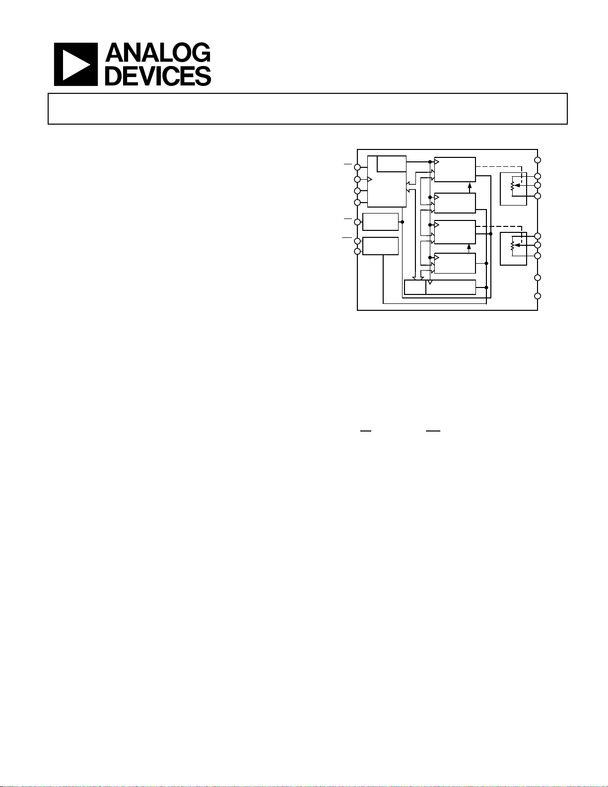
FUNCTIONAL BLOCK DIAGRAM
ADDR
CS
CLK
SDI
SDO
PR
WP
RDY
*RAB TOLERANCE
DECODE
SERIAL
INTERFACE
POWER-ON
RESET
EEMEM
CONTROL
RTOL*
RDAC1
REGISTER
EEMEM1
RDAC2
REGISTER
EEMEM2
26 BYTES
USER EEMEM
Figure 1.
In scratchpad programming mode, a specific setting can be
programmed directly to the RDAC
between Terminal W and Terminal A, and Terminal W and
Terminal B. This setting can be stored into the EEMEM and
is restored automatically to the RDAC register during system
power-on.
The EEMEM content can be restored dynamically or through
external
PR
strobing, and a WP function protects EEMEM contents.
To simplify the programming, the independent or simultaneous
linear-step increment or decrement commands can be used to move
the RDAC wiper up or down, one step at a time. For logarithmic
±6 dB changes in the wiper setting, the left or right bit shift
command can be used to double or halve the RDAC wiper setting.
The AD5235-EP patterned resistance tolerance is stored in the
EEMEM. Therefore, in readback mode, the host processor can
know the actual end-to-end resistance. The host can execute the
appropriate resistance step through a software routine that simplifies
open-loop applications as well as precision calibration and
tolerance matching applications.
The AD5235-EP is available in a thin, 16-lead TSSOP package.
The part is guaranteed to operate over the extended industrial
temperature range of −40°C to +125°C.
Full details about this enhanced product, including theory of
operation, register details, and applications information, are
available in the AD5235 data sheet, which should be consulted
in conjunction with this data sheet.
1
The terms nonvolatile memory and EEMEM are used interchangeably.
2
The terms digital potentiometer and RDAC are used interchangeably.
One Technology Way, P.O. Box 9106, Norwood, MA 02062-9106, U.S.A.
Tel: 781.329.4700 www.analog.com
Fax: 781.461.3113 ©2010–2012 Analog Devices, Inc. All rights reserved.
AD5235-EP
RDAC1
RDAC2
2
register that sets the resistance
V
DD
A1
W1
B1
A2
W2
B2
V
SS
GND
09185-001

AD5235-EP Enhanced Product
TABLE OF CONTENTS
Features .............................................................................................. 1
Applicat ions ....................................................................................... 1
General Description ......................................................................... 1
Functional Block Diagram .............................................................. 1
Revision History ............................................................................... 2
Specifications ..................................................................................... 3
Electrical Characteristics ............................................................. 3
Interface Timing and EEMEM Reliability Characteristics ..... 5
REVISION HISTORY
7/12—Rev. 0 to Rev. A
Change to Features Section .............................................................. 1
Changes to Electrical Characteristics Section and Table 1 .......... 3
Changes to Interface Timing and EEMEM Reliability
Characteristics Section and Table 2 ................................................ 5
Changes to Typical Performance Characteristics Section ............ 9
Added Figure 14 and Figure 16, Renumbered Sequentially ...... 10
Deleted Figure 21 ............................................................................. 11
Added Figure 23 ............................................................................... 12
7/10—Revision 0: Initial Version
Absolute Maximum Ratings ............................................................7
ESD Caution...................................................................................7
Pin Configuration and Function Descriptions ..............................8
Typical Performance Characteristics ..............................................9
Test Circuits ..................................................................................... 13
Outline Dimensions ....................................................................... 14
Ordering Guide .......................................................................... 14
Rev. A | Page 2 of 16

Enhanced Product AD5235-EP
SPECIFICATIONS
ELECTRICAL CHARACTERISTICS
VDD = 2.7 V to 5.5 V, VSS = 0 V; VDD = 2.5 V, VSS = −2.5 V, VA = VDD, VB = VSS, −40°C < TA < +125°C, unless otherwise noted.
Table 1.
Parameter Symbol Conditions Min Typ1 Max Unit
DC CHARACTERISTICS—RHEOSTAT MODE
(All RDACs)
Resistor Differential Nonlinearity2 R-DNL RWB −1 +1 LSB
Resistor Integral Nonlinearity2 R-INL RWB −2 +2 LSB
Nominal Resistor Tolerance ∆RAB/RAB Code = full scale −8 +8 %
Resistance Temperature Coefficient (∆RAB/RAB)/∆T × 106 35 ppm/°C
Wiper Resistance RW
Nominal Resistance Match R
DC CHARACTERISTICS—POTENTIOMETER
DIVIDER MODE (All RDACs)
Resolution N 10 Bits
Differential Nonlinearity3 DNL −1 +1 LSB
Integral Nonlinearity3 INL −1 +1 LSB
Voltage Divider Temperature Coefficient (∆VW/VW)/∆T × 106 Code = half scale 15 ppm/°C
Full-Scale Error V
Zero-Scale Error V
RESISTOR TERMINALS
Terminal Voltage Range4 V
Capacitance Ax, Bx5 C
Capacitance Wx5 C
Common-Mode Leakage Current
5, 6
DIGITAL INPUTS AND OUTPUTS
Input Logic High VIH With respect to GND, VDD = 5 V 2.4 V
Input Logic Low VIL With respect to GND, VDD = 5 V 0.8 V
Input Logic High VIH With respect to GND, VDD = 3 V 2.1 V
Input Logic Low VIL With respect to GND, VDD = 3 V 0.6 V
Input Logic High VIH
Input Logic Low VIL
Output Logic High (SDO, RDY) VOH R
Output Logic Low VOL I
Input Current IIL V
Input Capacitance5 C
= 1 V/RWB, VDD = 5 V, code =
I
W
30 65 Ω
half scale
= 1 V/RWB, VDD = 3 V, code =
I
W
50 Ω
half scale
Code = full scale, TA = 25°C ±0.1 %
AB1/RAB2
Code = full scale −7 0 LSB
WFSE
Code = zero scale 0 5 LSB
WZSE
, VB, VW V
A
A
, CB
f = 1 MHz, measured to GND,
VDD V
SS
11 pF
code = half-scale
W
f = 1 MHz, measured to GND,
80 pF
code = half-scale
ICM V
5 pF
IL
= VDD/2 0.01 ±1 μA
W
With respect to GND, V
= −2.5 V
V
SS
With respect to GND, V
= −2.5 V
V
SS
= 2.2 kΩ to 5 V 4.9 V
PULL-UP
= 1.6 mA, V
OL
= 0 V or VDD ±2.25 μA
IN
LOGI C
= +2.5 V,
DD
= +2.5 V,
DD
= 5 V 0.4 V
2.0 V
0.5 V
Rev. A | Page 3 of 16

AD5235-EP Enhanced Product
Parameter Symbol Conditions Min Typ1 Max Unit
POWER SUPPLIES
Single-Supply Power Range VDD V
Dual-Supply Power Range VDD/VSS ±2.25 ±2.75 V
Positive Supply Current IDD V
Negative Supply Current ISS
EEMEM Store Mode Current IDD (store)
I
EEMEM Restore Mode Current7 I
I
Power Dissipation8 P
Power Supply Sensitivity5 P
DYNAMIC CHARACTERISTICS
5, 9
(store) VDD = +2.5 V, VSS = −2.5 V −2 mA
SS
(restore)
DD
(restore) VDD = +2.5 V, VSS = −2.5 V −320 μA
SS
V
DISS
ΔVDD = 5 V ± 10% 0.006 0.01 %/%
SS
Bandwidth BW −3 dB, VDD/VSS = ±2.5 V 125 kHz
Total Harmonic Distortion THDW V
VW Settling Time tS
Resistor Noise Density e
T
N_WB
Crosstalk (CW1/CW2) CT
Analog Crosstalk CTA
1
Typicals represent average readings at 25°C and VDD = 5 V.
2
Resistor position nonlinearity error (R-INL) is the deviation from an ideal value measured between the maximum resistance and the minimum resistance wiper
positions. R-DNL measures the relative step change from ideal between successive tap positions. IW ~ 50 μA for VDD = 2.7 V and IW ~ 400 μA for VDD = 5 V (see Figure 25).
3
INL and DNL are measured at VW with the RDAC configured as a potentiometer divider similar to a voltage output DAC. VA = VDD and VB = VSS. DNL specification limits of
±1 LSB maximum are guaranteed monotonic operating conditions (see Figure 26).
4
Resistor Terminal A, Resistor Terminal B, and Resistor Terminal W have no limitations on polarity with respect to each other. Dual-supply operation enables ground-
referenced bipolar signal adjustment.
5
Guaranteed by design and not subject to production test.
6
Common-mode leakage current is a measure of the dc leakage from any Terminal A, Terminal B, or Terminal W to a common-mode bias level of VDD/2.
7
EEMEM restore mode current is not continuous. Current is consumed while EEMEM locations are read and transferred to the RDAC register (see Figure 22). To
minimize power dissipation, a NOP, Instruction 0 (0x0) should be issued immediately after Instruction 1 (0x1).
8
P
is calculated from (IDD × VDD) + (ISS × VSS).
DISS
9
All dynamic characteristics use VDD = +2.5 V and VSS = −2.5 V.
= 0 V 2.7 5.5 V
SS
= VDD or VIL = GND 2 7 μA
IH
= VDD or VIL = GND, VDD = +2.5 V,
V
IH
= −2.5 V
V
SS
= VDD or VIL = GND, VSS = GND,
V
IH
I
≈ 0
SS
= VDD or VIL = GND, VSS = GND,
V
IH
≈ 0
I
SS
= VDD or VIL = GND 10 40 μW
IH
= 1 V rms, VB = 0 V, f = 1 kHz 0.009 %
A
= VDD, VB = 0 V,
V
A
= 0.50% error band,
V
W
−6 −2 μA
2 mA
320 μA
4 μs
Code 0x000 to Code 0x200
= 25°C 20
A
= VDD, VB = 0 V, measured VW1
V
A
making full-scale change
with V
W2
= VA1 = +2.5 V,
V
DD
V
= VB1 = −2.5 V, measured
SS
with VW2 = 5 V p-p @ f = 1 kHz,
V
W1
30
−110
Code 1 = 0x200, Code 2 = 0x3FF
nV/√Hz
nV-s
dB
Rev. A | Page 4 of 16

Enhanced Product AD5235-EP
INTERFACE TIMING AND EEMEM RELIABILITY CHARACTERISTICS
Guaranteed by design and not subject to production test. See the Timing Diagrams section for the location of measured values. All input
control voltages are specified with t
measured using both V
= 2.7 V and VDD = 5 V.
DD
Table 2.
Parameter Symbol Conditions Min Typ1 Max Unit
Clock Cycle Time (t
) t1 20 ns
CYC
CS Setup Time
CLK Shutdown Time to CS Rise
Input Clock Pulse Width t4, t5 Clock level high or low 10 ns
Data Setup Time t6 From positive CLK transition 5 ns
Data Hold Time t7 From positive CLK transition 5 ns
CS to SDO-SPI Line Acquire
CS to SDO-SPI Line Release
CLK to SDO Propagation Delay2 t
CLK to SDO Data Hold Time t11 R
CS High Pulse Width3
CS High to CS High3
RDY Rise to CS Fall
CS Rise to RDY Fall Time
Store EEMEM Time
4, 5
Read EEMEM Time4 t
CS Rise to Clock Rise/Fall Setup
Preset Pulse Width (Asynchronous)6 t
Preset Response Time to Wiper Setting6 t
Power-On EEMEM Restore Time6 t
FLASH/EE MEMORY RELIABILITY
Endurance7 T
100
Data Retention8 100
1
Typicals represent average readings at 25°C and VDD = 5 V.
2
Propagation delay depends on the value of VDD, R
3
Valid for commands that do not activate the RDY pin.
4
The RDY pin is low only for Instruction 2, Instruction 3, Instruction 8, Instruction 9, Instruction 10, and the PR hardware pulse: CMD_8 ~ 20 μs; CMD_9, CMD_10 ~ 7 μs;
CMD_2, CMD_3 ~ 15 ms; PR hardware pulse ~ 30 μs.
5
Store EEMEM time depends on the temperature and EEMEM writes cycles. Higher timing is expected at a lower temperature and higher write cycles.
6
Not shown in Figure 2 and Figure 3.
7
Endurance is qualified to 100,000 cycles per JEDEC Standard 22, Method A117 and measured at −40°C, +25°C, and +125°C.
8
Retention lifetime equivalent at junction temperature (TJ) = 85°C per JEDEC Standard 22, Method A117. Retention lifetime based on an activation energy of 1 eV
derates with junction temperature in the Flash/EE memory.
= tF = 2.5 ns (10% to 90% of 3 V) and timed from a voltage level of 1.5 V. Switching characteristics are
R
t
10 ns
2
t
1 t
3
t
40 ns
8
t
50 ns
9
R
10
t
12
t
4 t
13
t
0 ns
14
t
0.15 0.3 ms
15
= 2.2 kΩ, CL < 20 pF 50 ns
P
= 2.2 kΩ, CL < 20 pF 0 ns
P
10 ns
CYC
CYC
t16 Applies to Instructions 0x2, 0x3 15 50 ms
Applies to Instructions 0x8, 0x9, 0x10 7 30 μs
16
t
10 ns
17
50 ns
PRW
PRESP
30 μs
EEMEM
, and CL.
PULL-UP
pulsed low to refresh wiper positions
PR
= 25°C 1
A
30 μs
MCycles
kCycles
Yea r s
Rev. A | Page 5 of 16

AD5235-EP Enhanced Product
*
Timing Diagrams
CPHA= 1
CS
t
t
CLK
CPOL = 1
HIGH
OR LOW
SDI
SDO
t
14
RDY
THE EXTRA BIT THAT IS NOT DEFINED IS NORMALLY THE LSB OF THE CHARACT ER PREVIOUSLY TRANSMITTED.
THE CPOL = 1 MI CROCONTROL LER COMMAND ALIGNS THE INCOMING DATA TO THE P OSITI VE EDGE OF THE CLOCK.
2
t
8
B24* B23 (MSB) B0 (LSB)
1
t
B23 B0
5
t
4
t
7
t
6
B23 (MSB)
t
10
t
11
B0 (LSB)
t
3
t
12
t
13
t
17
HIGH
OR LOW
t
9
t
15
t
16
09185-002
Figure 2. CPHA = 1 Timing Diagram
CPHA = 0
CLK
CPOL = 0
SDI
CS
HIGH
OR LOW
t
2
B23 (MSB IN)
t
1
t
B23 B0
5
t
4
t
7
t
6
B0 (LSB)
t
3
t
12
t
13
t
17
HIGH
OR LOW
t
8
SDO
t
14
RDY
*THE EXTRA BIT THAT IS NO T DEFINED IS NORMALL Y THE MSB OF THE CHARACTER JUST RECEIVED.
THE CPOL = 0 MICRO CONTROL LER COMMAND ALIGNS THE INCOMI NG DATA TO THE PO SITIVE EDGE OF THE CLOCK.
B23 (MSB OUT) B0 (LSB)
t
10
t
11
t
9
*
t
15
t
16
9185-003
Figure 3. CPHA = 0 Timing Diagram
Rev. A | Page 6 of 16

Enhanced Product AD5235-EP
ABSOLUTE MAXIMUM RATINGS
TA = 25°C, unless otherwise noted.
Table 3.
Parameter Rating
VDD to GND –0.3 V to +7 V
VSS to GND +0.3 V to −7 V
VDD to VSS 7 V
VA, VB, VW to GND VSS − 0.3 V to VDD + 0.3 V
IA, IB, IW
Pulsed1 ±2.5 mA
Continuous ±1.1 mA
Digital Input and Output Voltage to GND −0.3 V to VDD + 0.3 V
Operating Temperature Range2 −40°C to +125°C
Maximum Junction Temperature (TJ max) 150°C
Storage Temperature Range −65°C to +150°C
Lead Temperature, Soldering
Vapor Phase (60 sec) 215°C
Infrared (15 sec) 220°C
Thermal Resistance
Junction-to-Ambient, θJA 150°C/W
Junction-to-Case, θJC 28°C/W
Package Power Dissipation (TJ max − TA)/θJA
1
Maximum terminal current is bounded by the maximum current handling of
the switches, maximum power dissipation of the package, and maximum
applied voltage across any two of the A, B, and W terminals at a given
resistance.
2
Includes programming of nonvolatile memory.
Stresses above those listed under Absolute Maximum Ratings
may cause permanent damage to the device. This is a stress
rating only; functional operation of the device at these or any
other conditions above those indicated in the operational
section of this specification is not implied. Exposure to absolute
maximum rating conditions for extended periods may affect
device reliability.
ESD CAUTION
Rev. A | Page 7 of 16

AD5235-EP Enhanced Product
PIN CONFIGURATION AND FUNCTION DESCRIPTIONS
1
CLK
2
SDI
3
SDO
4
GND
V
SS
A1
W1
B1
AD5235-EP
TOP VIEW
5
(Not to Scale)
6
7
8
Figure 4. Pin Configuration
16
RDY
15
CS
14
PR
13
WP
12
V
DD
11
A2
10
W2
9
B2
09185-004
Table 4. Pin Function Descriptions
Pin No. Mnemonic Description
1 CLK Serial Input Register Clock. Shifts in one bit at a time on positive clock edges.
2 SDI Serial Data Input. Shifts in one bit at a time on positive clock CLK edges. MSB loads first.
3 SDO
Serial Data Output. Serves readback and daisy-chain functions. Command 9 and Command 10 activate the SDO
output for the readback function, delayed by 24 or 25 clock pulses, depending on the clock polarity before and
after the data-word (see Figure 2 and Figure 3). In other commands, the SDO shifts out the previously loaded SDI
bit pattern, delayed by 24 or 25 clock pulses depending on the clock polarity (see Figure 2 and Figure 3). This
previously shifted out SDI can be used for daisy-chaining multiple devices. Whenever SDO is used, a pull-up
resistor in the range of 1 kΩ to 10 kΩ is needed.
4 GND Ground Pin, Logic Ground Reference.
5 VSS
Negative Supply. Connect to 0 V for single-supply applications. If V
is used in dual supply, it must be able to sink
SS
35 mA for 30 ms when storing data to EEMEM.
6 A1 Terminal A of RDAC1.
7 W1 Wiper terminal of RDAC1. ADDR (RDAC1) = 0x0.
8 B1 Terminal B of RDAC1.
9 B2 Terminal B of RDAC2.
10 W2 Wiper terminal of RDAC2. ADDR (RDAC2) = 0x1.
11 A2 Terminal A of RDAC2.
12 VDD Positive Power Supply.
13
Optional Write Protect. When active low, WP prevents any changes to the present contents, except PR strobe.
WP
CMD_1 and COMD_8 refresh the RDAC register from EEMEM. Execute a NOP instruction before returning to WP
14
15
Optional Hardware Override Preset. Refreshes the scratchpad register with current contents of the EEMEM
PR
Serial Register Chip Select Active Low. Serial register operation takes place when CS returns to logic high.
CS
16 RDY
high. Tie WP
register. Factory default loads midscale 512
at the logic high transition. Tie PR
Ready. Active high open-drain output. Identifies completion of Instruction 2, Instruction 3, Instruction 8,
Instruction 9, Instruction 10, and PR
to VDD, if not used.
until EEMEM is loaded with a new value by the user. PR is activated
10
to VDD, if not used.
.
Rev. A | Page 8 of 16

Enhanced Product AD5235-EP
TYPICAL PERFORMANCE CHARACTERISTICS
0.25
–40
+25
0.20
+85
+125
0.15
0.10
0.05
0
INL ERROR (LSB)
0.05
0.10
0.15
0.20
0 200 400 600 800 1000
DIGITAL CODE
Figure 5. INL vs. Code, T
= −40°C, +25°C, +85°C, +125°C Overlay
A
09185-005
0.20
0.15
0.10
0.05
0
R-DNL ERROR (L SB)
–0.05
–0.10
–0.15
0 200 400 600 800 1000
DIGITAL CODE
–40
+25
+85
+125
Figure 8. R-DNL vs. Code, TA = −40°C, +25°C, +85°C, +125°C Overlay
09185-008
0.16
–40
+25
0.14
+85
+125
0.12
0.10
0.08
0.06
0.04
DNL ERROR (LSB)
0.02
0
0.02
0.04
0 200 400 600 800 1000
DIGITAL CODE
Figure 6. DNL vs. Code, TA = −40°C, +25°C, +85°C, +125°C Overlay
0.20
–40
+25
+85
0.15
+125
0.10
0.05
0
0.05
R-INL ERROR ( LSB)
0.10
0.15
0.20
0 200 400 600 800 1000
DIGITAL CODE
Figure 7. R-INL vs. Code, TA = −40°C, +25°C, +85°C, +125°C Overlay,
200
180
160
140
120
100
80
60
40
20
POTENTI OMETE R MODE TEMPCO (ppm/°C)
0
0 1023768512256
09185-006
CODE (Deci mal)
09185-009
Figure 9. (∆VW/VW)/∆T × 106 Potentiometer Mode Tempco
200
180
160
140
120
100
80
60
40
RHEOSTAT MODE TEMP CO (ppm/ °C)
20
0
0 1023768512256
09185-007
CODE (Decimal )
09185-010
Figure 10. (∆RWB/RWB)/∆T × 106 Rheostat Mode Tempco
Rev. A | Page 9 of 16

AD5235-EP Enhanced Product
60
50
40
30
20
WIPER ON RESISTANCE (Ω)
10
0
0 200 400 800600 1000
CODE (Decimal )
Figure 11. Wiper On Resistance vs. Code
3
IDD = 2.7V
IDD = 3.3V
IDD = 3.0V
2
IDD = 5.0V
IDD = 5.5V
1
(µA)
0
SS
/I
DD
I
–1
ISS = 2.7V
–2
–3
ISS = 3.3V
ISS = 3.0V
ISS = 5.0V
ISS = 5.5V
–55 –50 –40 –20 0 25 40 60 85 100 110 125
TEMPERAT URE (°C)
Figure 12. IDD vs. Temperature
2.7V
3.0V
3.3V
5.0V
5.5V
2.7V
400
300
(µA)
DD
200
I
100
0
012345
09185-011
VDIO (V)
3.0V
3.3V
5.0V
5.5V
09185-014
Figure 14. IDD vs. Digital Input Voltage
0.12
0.10
0.08
0.06
THD + N (%)
0.04
0.02
0
10 100 1k 10k 100k
09185-012
FREQUENC Y (Hz)
09185-015
Figure 15. THD + Noise vs. Frequency
50
FULL SCALE
MIDSCALE
ZERO SCALE
40
30
(µA)
DD
I
20
10
0
11098765432
FREQUENCY (MHz)
09185-013
Figure 13. IDD vs. Clock Frequency
10
1
0.1
THD + N (%)
0.01
0.001
0.0001 0.001 0. 01 0.1 1 10
AMPLITUDE (V rms)
Figure 16. THD + Noise vs. Amplitude
09185-016
Rev. A | Page 10 of 16

Enhanced Product AD5235-EP
3
0
–3
–6
GAIN (dB)
f
= 125kHz
–3dB
–9
–12
1k 10 k 100k 1M
= ±2.5V
V
DD/VSS
V
= 1V rms
A
D = MIDSCALE
FREQUENC Y (Hz)
Figure 17. −3 dB Bandwidth vs. Resistance (See Figure 31)
0
CODE 0x200
–10
0x100
0x080
–20
0x040
0x020
–30
GAIN (dB)
0x010
0x008
–40
0x004
0x002
–50
0x001
–60
1k 10k 100k 1M
FREQUENCY (Hz)
Figure 18. Gain vs. Frequency vs. Code, (See Figure 31)
V
DD
VW (FULL SCALE)
VDD = 5V
= 5V
V
A
= 0V
V
B
= 25°C
T
09185-017
10µs/DIV
A
1V/DIV
09185-020
Figure 20. Power-On Reset
2.5196
2.516
2.512
2.508
2.504
2.500
2.496
AMPLIT UDE (V)
2.492
2.488
2.484
2.4796
0 20406080100120
09185-018
TIME (µs)
V
= VSS= 5V
DD
CODE = 0x200 TO 0x1FF
144
09185-021
Figure 21. Midscale Glitch Energy
0
VDD = 5V ± 10% AC
= 0V, VA = 4V, VB = 0V
V
SS
–10
MEASURED AT V
= 25°C
T
A
–20
–30
–40
PSRR (dB)
–50
–60
–70
–80
10 100 1k 10k 100k 1M
WITH CO DE = 0x200
W
FREQUENC Y (Hz)
Figure 19. PSRR vs. Frequency
09185-019
Rev. A | Page 11 of 16
CS (5V/DIV)
CLK (5V/DIV)
SDI (5V/DIV)
VDD = 5V
T
IDD (2mA/DIV)
= 25°C
A
Figure 22. IDD vs. Time when Storing Data to EEMEM
02816-023

AD5235-EP Enhanced Product
2.60
100
VA = VB = OPEN
= 25°C
T
A
2.55
2.50
WIPER VOLTAGE (V)
2.45
2.40
0 0.5 1.0 1.5 2.0
TIME (µs)
Figure 23. Digital Feedthrough
09185-024
10
– mA)
WB_MAX
1
0.1
THEORECT ICAL (I
0.01
Figure 24. I
= 25kΩ
R
AB
CODE (Decimal )
vs. Code
WB_MAX
1023
896768640512384128 2560
09185-125
Rev. A | Page 12 of 16

Enhanced Product AD5235-EP
V
V
V
V
TEST CIRCUITS
Figure 25 to Figure 35 define the test conditions used in the Specifications section.
NC
DUT
A
W
B
NC = NO CONNECT
Figure 25. Resistor Position Nonlinearity Error (Rheostat Operation; R-INL, R-DNL)
DUT
A
V+
W
B
Figure 26. Potentiometer Divider Nonlinearity Error (INL, DNL)
I
W
V
MS
V+ = V
1LSB = V+/2
V
A
V
IN
OFFSET
GND
09185-026
DUT
W
B
2.5V
+15
OP42
–15V
V
OUT
09185-032
Figure 31. Gain vs. Frequency
0.1
RSW=
DUT
DD
N
MS
09185-027
B
A = NC
W
I
SW
V
I
CODE = 0x00
TO V
SS
DD
SW
+
0.1V
–
09185-033
Figure 32. Incremental On Resistance
NC
I
DUT
A
V
W
V
MS2
W
B
= VDD/R
W
V
RW = [V
MS1
Figure 27. Wiper Resistance
A
V
A
DD
V+
~
W
B
V
MS
V+ = VDD ±10%
PSRR (dB) = 20 L OG
PSS (%/%) =
Figure 28. Power Supply Sensitivity (PSS, PSRR)
ABDUT
W
OP279
OFFSET BIAS
OFFSET
GND
V
IN
Figure 29. Inverting Gain
5
V
NOMI NAL
– V
MS1
MS2
]/I
W
09185-028
DD
DUT
V
SS
Figure 33. Common-Mode Leakage Current
V
IN
V
∆
MS
)
(
∆V
∆V
∆V
5V
DD
%
MS
%
DD
09185-029
TO OUTPUT
V
OUT
09185-030
PIN
Figure 35. Load Circuit for Measuring VOH and VOL (The diode bridge test
circuit is equivalent to the application circuit with R
A
GND
B
NC
NC = NO CONNECT
A1
RDAC1 RDAC2
W1
NC
B1
CTA = 20 LOG[V
NC = NO CONNECT
I
CM
W
V
CM
V
DD
A2
W2
B2
V
SS
]
OUT/VIN
Figure 34. Analog Crosstalk
200µAI
C
L
50pF
200µAI
OL
OH
9185-034
V
OUT
VOH (MIN)
OR
V
(MAX)
OL
PULL-UP
9185-035
09185-036
of 2.2 kΩ.)
OP279
W
OFFSET
GND
V
IN
ABDUT
OFFSET BIAS
Figure 30. Noninverting Gain
V
OUT
09185-031
Rev. A | Page 13 of 16

AD5235-EP Enhanced Product
OUTLINE DIMENSIONS
5.10
5.00
4.90
0.15
0.05
4.50
4.40
4.30
PIN 1
16
0.65
BSC
COPLANARITY
COMPLIANT TO JEDEC STANDARDS MO-153-AB
0.10
0.30
0.19
9
81
1.20
MAX
SEATING
PLANE
6.40
BSC
0.20
0.09
8°
0°
0.75
0.60
0.45
Figure 36. 16-Lead Thin Shrink Small Outline Package [TSSOP]
(RU-16)
Dimensions shown in millimeters
ORDERING GUIDE
Model R
AD5235BRU25-EP-RL7 25 −40°C to +125°C 16-Lead TSSOP RU-16
(kΩ) Temperature Range Package Description Package Option
AB
Rev. A | Page 14 of 16

Enhanced Product AD5235-EP
NOTES
Rev. A | Page 15 of 16

AD5235-EP Enhanced Product
NOTES
©2010–2012 Analog Devices, Inc. All rights reserved. Trademarks and
registered trademarks are the property of their respective owners.
D09185-0-7/12(A)
Rev. A | Page 16 of 16
 Loading...