

Nonvolatile Memory,
V
S
Dual 256-Position Digital Potentiometer
Data Sheet
FEATURES
Dual-channel, 256-position resolution
10 kΩ, 50 kΩ, and 100 kΩ nominal terminal resistance
Nonvolatile memory maintenance of wiper settings
Predefined linear increment/decrement instructions
Predefined ±6 dB step log taper increment/decrement
instructions
SPI-compatible serial interface
Wiper settings and EEMEM readback
3 V to 5 V single-supply operation
±2.5 V dual-supply operation
14 bytes of general-purpose user EEMEM
Permanent memory write protection
100-year typical data retention (T
APPLICATIONS
Mechanical potentiometer replacement
Instrumentation: gain and offset adjustment
Programmable voltage-to-current conversion
Programmable filters, delays, and time constants
Programmable power supply
Low resolution DAC replacement
Sensor calibration
= 55°C)
A
CS
CLK
SDI
DO
PR
WP
RDY
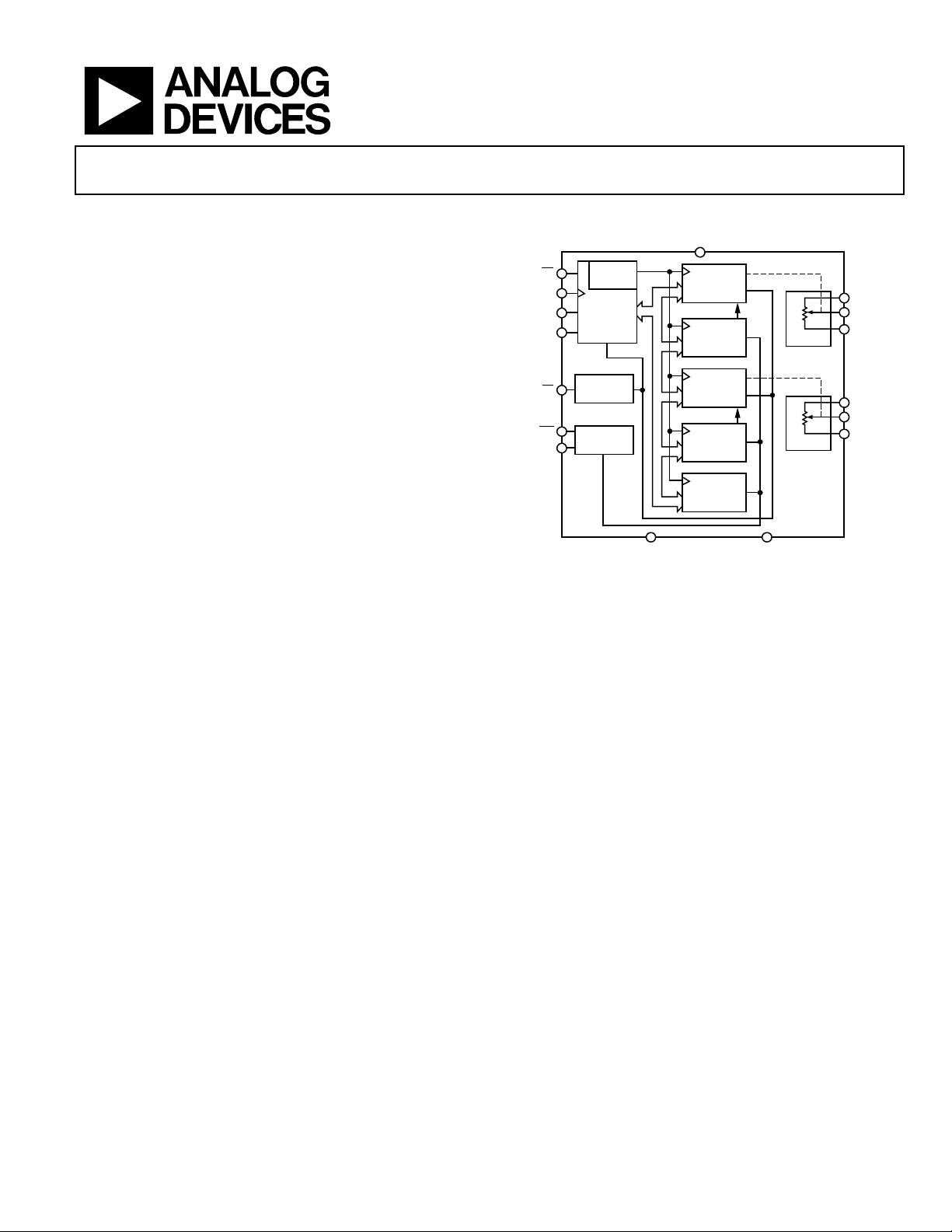
FUNCTIONAL BLOCK DIAGRAM
DD
V
SS
AD5232
ADDR
DECODE
SERIAL
INTERFACE
POWER-ON
RESET
EEMEM
CONTROL
GND
RDAC1
REGISTER
EEMEM1
RDAC2
REGISTER
EEMEM2
14 BYTES
USER
EEMEM
Figure 1.
AD5232
A1
W1
RDAC1
RDAC2
B1
A2
W2
B2
02618-001
GENERAL DESCRIPTION
The AD5232 device provides a nonvolatile, dual-channel,
digitally controlled variable resistor (VR) with 256-position
resolution. This device performs the same electronic adjustment
function as a mechanical potentiometer with enhanced resolution,
solid state reliability, and superior low temperature coefficient
performance. The versatile programming of the AD5232, perormed via a microcontroller, allows multiple modes of operation
and adjustment.
In the direct program mode, a predetermined setting of the RDAC
registers (RDAC1 and RDAC2) can be loaded directly from the
microcontroller. Another important mode of operation allows
the RDACx register to be refreshed with the setting previously
stored in the corresponding EEMEM register (EEMEM1 and
EEMEM2). When changes are made to the RDACx register to
establish a new wiper position, the value of the setting can be
saved into the EEMEMx register by executing an EEMEM save
operation. After the settings are saved in the EEMEMx register,
these values are automatically transferred to the RDACx register
to set the wiper position at system power-on. Such operation is
enabled by the internal preset strobe. The preset strobe can also
be accessed externally.
Rev. B
Information furnished by Analog Devices is believed to be accurate and reliable. However, no
responsibility is assumed by Anal og Devices for its use, nor for any infringements of patents or ot her
rights of third parties that may result from its use. Specifications subject to change without notice. No
license is granted by implication or otherwise under any patent or patent rights of Analog Devices.
Trademarks and registered trademarks are the proper ty of their respec tive owners.
All internal register contents can be read via the serial data
output (SDO). This includes the RDAC1 and RDAC2 registers,
the corresponding nonvolatile EEMEM1 and EEMEM2 registers,
and the 14 spare USER EEMEM registers that are available for
constant storage.
The basic mode of adjustment is the increment and decrement
command instructions that control the wiper position setting
register (RDACx). An internal scratch pad RDACx register can
be moved up or down one step of the nominal resistance between
Terminal A and Terminal B. This step adjustment linearly changes
the wiper to Terminal B resistance (R
of the device’s end-to-end resistance (R
) by one position segment
WB
). For exponential/
AB
logarithmic changes in wiper setting, a left/right shift command
instruction adjusts the levels in ±6 dB steps, which can be useful
for audio and light alarm applications.
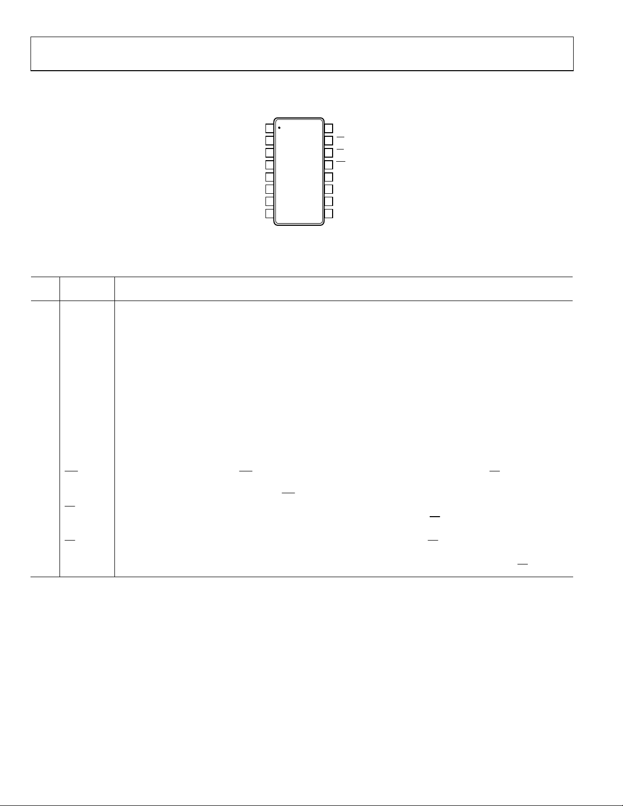
The AD5232 is available in a thin, 16-lead TSSOP package.
All parts are guaranteed to operate over the extended industrial
temperature range of −40°C to +85°C. An evaluation board, the
EVAL-AD5232-10EBZ, is available.
One Technology Way, P.O. Box 9106, Norwood, MA 02062-9106, U.S.A.
Tel: 781.329.4700 www.analog.com
Fax: 781.461.3113 ©2001–2011 Analog Devices, Inc. All rights reserved.

AD5232 Data Sheet
TABLE OF CONTENTS
Features.............................................................................................. 1
Applications....................................................................................... 1
Functional Block Diagram .............................................................. 1
General Description ......................................................................... 1
Revision History ............................................................................... 2
Specifications..................................................................................... 3
Electrical Characteristics—10 kΩ, 50 kΩ, 100 kΩ Versions .. 3
Interface Timing Characteristics................................................ 5
Absolute Maximum Ratings............................................................ 7
Thermal Resistance ...................................................................... 7
ESD Caution.................................................................................. 7
Pin Configuration and Function Descriptions............................. 8
Typical Performance Characteristics ............................................. 9
Test Circuits..................................................................................... 12
Theory of Operation ...................................................................... 14
Scratch Pad and EEMEM Programming................................. 14
Basic Operation .......................................................................... 14
EEMEM Protection.................................................................... 14
Digital Input/Output Configuration........................................ 14
Serial Data Interface................................................................... 15
Daisy-Chaining Operation........................................................ 15
Advanced Control Modes ......................................................... 17
Using Additional Internal, Nonvolatile EEMEM................... 18
Terminal Voltage Operating Range ......................................... 18
Detailed Potentiometer Operation .......................................... 18
Programming the Variable Resistor......................................... 19
Programming the Potentiometer Divider............................... 20
Operation from Dual Supplies ................................................. 20
Application Programming Examples ...................................... 20
Equipment Customer Start-up Sequence
for a PCB Calibrated Unit with Protected Settings................ 21
Flash/EEMEM Reliability.......................................................... 21
Evaluation Board........................................................................ 21
Outline Dimensions....................................................................... 22
Ordering Guide .......................................................................... 22
REVISION HISTORY
09/11—Rev. A to Rev. B
Change to Resistor Noise Voltage Parameter in Table 1.............. 4
10/09—Rev. 0 to Rev. A
Updated Format ..................................................................Universal
Changes to Data Sheet Title............................................................ 1
Changes to Features Section............................................................ 1
Changes to Applications Section .................................................... 1
Change to Wiper Resistance Parameter, Table 1 .......................... 3
Changes to
Changes to Figure 2 and Figure 3....................................................6
Changes to Figure 24...................................................................... 12
Added Figure 32 ............................................................................. 13
Changes to Serial Data Interface Section .................................... 15
Changes to Programming the Variable Resistor Section .......... 19
Changes to Ordering Guide.......................................................... 22
10/01—Revision 0: Initial Version
CS
Rise to RDY Fall Time Parameter, Table 2 ..........5
Rev. B | Page 2 of 24

Data Sheet AD5232
SPECIFICATIONS
ELECTRICAL CHARACTERISTICS—10 kΩ, 50 kΩ, 100 kΩ VERSIONS
VDD = 3 V ± 10% or 5 V ± 10% and VSS = 0 V, VA = +VDD, VB = 0 V, −40°C < TA < +85°C, unless otherwise noted.
Table 1.
Parameter Symbol Conditions Min Typ1 Max Unit
DC CHARACTERISTICS,
RHEOSTAT MODE
Resistor Differential Nonlinearity2 R-DNL RWB, VA = NC −1 ±1/2 +1 LSB
Resistor Nonlinearity2 R-INL RWB, VA = NC −0.4 +0.4 % FS
Nominal Resistor Tolerance ∆RAB −40 +20 %
Resistance Temperature Coefficient ∆RAB/∆T 600 ppm/°C
Wiper Resistance RW IW = 100 μA, VDD = 5.5 V, code = 0x1E 50 100 Ω
I
POTENTIOMETER DIVIDER MODES
Resolution N 8 Bits
Differential Nonlinearity3 DNL −1 ±1/2 +1 LSB
Integral Nonlinearity3 INL −0.4 +0.4 % FS
Voltage Divider Temperature
Coefficient
Full-Scale Error V
Zero-Scale Error V
RESISTOR TERMINALS
Terminal Voltage Range4 VA, VB, VW VSS VDD V
Capacitance Ax, Bx5 C
Capacitance Wx5 C
Common-Mode Leakage Current
DIGITAL INPUTS AND OUTPUTS
Input Logic High VIH With respect to GND, VDD = 5 V 2.4 V
Input Logic Low VIL With respect to GND, VDD = 5 V 0.8 V
Input Logic High VIH With respect to GND, VDD= 3 V 2.1 V
Input Logic Low VIL With respect to GND, VDD = 3 V 0.6 V
Input Logic High VIH With respect to GND, VDD = +2.5 V, VSS = −2.5 V 2.0 V
Input Logic Low VIL With respect to GND, VDD = +2.5 V, VSS = −2.5 V 0.5 V
Output Logic High (SDO and RDY) VOH R
Output Logic Low VOL IOL = 1.6 mA, V
Input Current IIL VIN = 0 V or VDD ±2.5 μA
Input Capacitance5 CIL 4 pF
POWER SUPPLIES
Single-Supply Power Range VDD V
Dual-Supply Power Range VDD/VSS ±2.25 ±2.75 V
Positive Supply Current IDD VIH = VDD or VIL = GND 3.5 10 μA
Programming Mode Current I
Read Mode Current7 I
Negative Supply Current ISS VIH = VDD or VIL = GND,
V
Power Dissipation8 P
Power Supply Sensitivity5 PSS ∆VDD = 5 V ± 10% 0.002 0.01 %/%
Specifications apply to all VRs
= 100 μA, VDD = 3 V, code = 0x1E 200 Ω
W
∆V
/ΔT Code = half scale 15 ppm/°C
W
Code = full scale −3 0 % FS
WFSE
Code = zero scale 0 3 % FS
WZSE
, CB f = 1 MHz, measured to GND, code = half-scale 45 pF
A
f = 1 MHz, measured to GND, code = half scale 60 pF
5, 6
W
ICM VW = VDD/2 0.01 1 μA
= 2.2 kΩ to 5 V 4.9 V
PULL-UP
= 5 V 0.4 V
LOGI C
= 0 V 2.7 5.5 V
SS
VIH = VDD or VIL = GND 35 mA
DD(PG)
VIH = VDD or VIL = GND 0.9 3 9 mA
DD(XFR)
= +2.5 V, VSS = −2.5 V 3.5 10 μA
DD
VIH = VDD or VIL = GND 0.018 0.05 mW
DISS
Rev. B | Page 3 of 24

AD5232 Data Sheet
Parameter Symbol Conditions Min Typ1 Max Unit
DYNAMIC CHARACTERISTICS
Bandwidth −3 dB, BW_10kΩ, R = 10 kΩ 500 kHz
Total Harmonic Distortion THDw VA = 1 V rms, VB = 0 V, f = 1 kHz, RAB = 10 kΩ 0.022 %
V
VW Settling Time tS V
V
for RAB = 10 kΩ/50 kΩ/100 kΩ
Resistor Noise Voltage e
Crosstalk (CW1/CW2) CT V
adjacent VR making full-scale code change
Analog Crosstalk (CW1/CW2) CTA V
5 V p-p @ f = 10 kHz; Code1 = 0x80; Code2 = 0xFF
FLASH/EE MEMORY RELIABILITY
Endurance10 100
Data Retention11 100
1
Typical parameters represent average readings at 25°C and VDD = 5 V.
2
Resistor position nonlinearity (R-INL) error is the deviation from an ideal value measured between the maximum resistance and the minimum resistance wiper
positions. R-DNL measures the relative step change from ideal between successive tap positions. Parts are guaranteed monotonic. IW ~ 50 μA @ VDD = 2.7 V and IW ~
400 μA @ VDD = 5 V for the RAB = 10 kΩ version, IW ~ 50 μA for the RAB = 50 kΩ version, and IW ~ 25 μA for the RAB = 100 kΩ version (see Figure 22).
3
INL and DNL are measured at VW with the RDACx configured as a potentiometer divider similar to a voltage output digital-to-analog converter. VA = VDD and VB = VSS.
DNL specification limits of ±1 LSB maximum are guaranteed monotonic operating conditions (see Figure 23).
4
The A, B, and W resistor terminals have no limitations on polarity with respect to each other. Dual supply operation enables ground-referenced bipolar signal
adjustment.
5
Guaranteed by design; not subject to production test.
6
Common-mode leakage current is a measure of the dc leakage from any A, B, or W terminal to a common-mode bias level of VDD/2.
7
Transfer (XFR) mode current is not continuous. Current is consumed while the EEMEMx locations are read and transferred to the RDACx register (see Figure 13).
8
P
is calculated from (IDD × VDD) + (ISS × VSS).
DISS
9
All dynamic characteristics use VDD = +2.5 V and VSS = −2.5 V, unless otherwise noted.
10
Endurance is qualified to 100,000 cycles per JEDEC Std. 22, Method A117 and measured at −40°C, +25°C, and +85°C. Typical endurance at +25°C is 700,000 cycles.
11
The retention lifetime equivalent at junction temperature (T
derates with junction temperature as shown in Figure 44 in the Flash/EEMEM Reliability section. The AD5232 contains 9,646 transistors. Die size = 69 mil × 115 mil,
7,993 sq. mil.
5, 9
= 1 V rms, VB = 0 V, f = 1 kHz, RAB = 50 kΩ, 100 kΩ 0.045 %
A
= 5 V, VSS = 0 V, VA = VDD, VB = 0 V, 0.65/3/6 μs
DD
= 0.50% error band, Code 0x00 to Code 0x80
W
RWB = 5 kΩ, f= 1 kHz 9 nV/√Hz
N_WB
= VDD, VB = 0 V, measure VW with −5 nV-sec
A
= VDD, VB1 = 0 V, measure VW1 with VW2 = −70 dB
A1
) = 55°C, as per JEDEC Std. 22, Method A117. Retention lifetime, based on an activation energy of 0.6 eV,
J
kCycles
Yea r s
Rev. B | Page 4 of 24
Data Sheet AD5232
INTERFACE TIMING CHARACTERISTICS
All input control voltages are specified with tR = tF = 2.5 ns (10% to 90% of 3 V) and are timed from a voltage level of 1.5 V. Switching
characteristics are measured using both V
= 3 V and VDD = 5 V.
DD
Table 2.
Parameter
Clock Cycle Time (t
CS Setup Time
CLK Shutdown Time to CS Rise
1, 2
Symbol Conditions Min Typ3 Max Unit
) t1 20 ns
CYC
t
10 ns
2
t
1 t
3
CYC
Input Clock Pulse Width t4, t5 Clock level high or low 10 ns
Data Setup Time t6 From positive CLK transition 5 ns
Data Hold Time t7 From positive CLK transition 5 ns
t
CS to SDO-SPI Line Acquire
CS to SDO-SPI Line Release
CLK to SDO Propagation Delay4 t
CLK to SDO Data Hold Time t11 R
CS High Pulse Width5
CS High to CS High5
RDY Rise to CS Fall
CS Rise to RDY Fall Time
Store/Read EEMEM Time6 t
40 ns
8
t
50 ns
9
R
10
t
12
t
4 t
13
t
0 ns
14
t
0.15 0.3 ms
15
16
= 2.2 kΩ, CL < 20 pF 50 ns
P
= 2.2 kΩ, CL < 20 pF 0 ns
P
Applies to Command Instruction 2, Command
10 ns
25 ms
CYC
Instruction 3, and Command Instruction 9
t
CS Rise to Clock Rise/Fall Setup
Preset Pulse Width (Asynchronous) t
Preset Response Time to RDY High t
1
Guaranteed by design; not subject to production test.
2
See the Timing Diagrams section for the location of measured values.
3
Typicals represent average readings at 25°C and VDD = 5 V.
4
Propagation delay depends on the value of VDD, R
5
Valid for commands that do not activate the RDY pin.
6
RDY pin low only for Command Instruction 2, Command Instruction 3, Command Instruction 8, Command Instruction 9, Command Instruction 10, and the PR hardware pulse:
CMD_8 ~ 1 ms, CMD_9 = CMD_10 ~ 0.12 ms, and CMD_2 = CMD_3 ~ 20 ms. Device operation at TA = −40°C and VDD < 3 V extends the save time to 35 ms.
10 ns
17
Not shown in timing diagram 50 ns
PRW
PRESP
PULL-UP
, and CL.
pulsed low to refresh wiper positions
PR
70 μs
Rev. B | Page 5 of 24
AD5232 Data Sheet
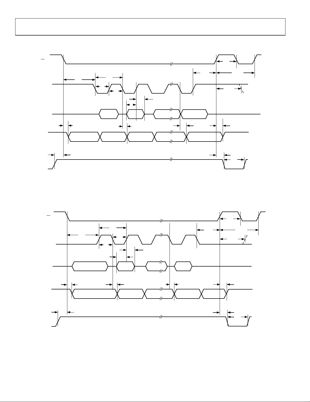
Timing Diagrams
CPHA = 1
CS
t
B0
(LSB)
3
B0
(LSB)
t
t
CLK
CPOL = 1
HIGH
OR LOW
SDI
SDO
t
14
RDY
NOTES
1. B24 IS AN EXT RA BIT THAT IS NOT DEF INED, BUT I T IS USUAL LY THE LSB OF THE CHARACT ER THAT WAS PREVIOUSL Y TRANSMIT TED.
2. THE CPOL = 1 MICROCO NTROLL ER COMMAND ALI GNS THE I NCOMING DAT A TO THE POSITI VE EDGE O F THE CLOCK.
2
t
8
B16*
1
t
B15 B0
5
t
4
t
7
t
6
B15
(MSB)
t
10
B15
(MSB)
t
11
t
12
t
13
t
17
HIGH
OR LOW
t
9
t
15
t
16
02618-002
Figure 2. CPHA = 1
CPHA = 0
CLK
CPOL = 0
SDI
CS
HIGH
OR LOW
B15
(MSB)
t
2
B15
(MSB IN)
t
1
t
B15 B0
5
t
4
t
7
t
6
B0
(LSB)
B0
(LSB)
t
3
t
12
t
13
t
17
HIGH
OR LOW
t
8
SDO
t
14
RDY
NOTES
1. THIS EXTRA BIT IS NOT DEFI NED, BUT IT IS USUALL Y THE MSB OF THE CHARACTER T HAT WAS JUST RECEIVED.
2. THE CPOL = 0 MICROCO NTROLL ER COMMAND ALI GNS THE I NCOMING DAT A TO THE POSITI VE EDGE O F THE CLOCK.
B15
(MSB OUT)
t
10
t
11
B0
(LSB)
*
Figure 3. CPHA = 0
Rev. B | Page 6 of 24
t
9
t
15
t
16
02618-003
Data Sheet AD5232
ABSOLUTE MAXIMUM RATINGS
= 25°C, unless otherwise noted.
A
Table 3.
Parameter Rating
VDD to GND −0.3 V, +7 V
VSS to GND +0.3 V, −7 V
VDD to VSS 7 V
VA, VB, VW to GND VSS − 0.3 V, VDD + 0.3 V
AX − BX, AX − WX, BX − WX
Intermittent
1
±20 mA
Continuous ±2 mA
Digital Inputs and Output Voltage to GND −0.3 V, VDD + 0.3 V
Operating Temperature Range2 −40°C to +85°C
Maximum Junction Temperature (TJ max) 150°C
Storage Temperature Range −65°C to +150°C
Lead Temperature, Soldering
Vapor Phase (60 sec) 215°C
Infrared (15 sec) 220°C
Package Power Dissipation (TJ max − TA)/θJA
1
Maximum terminal current is bounded by the maximum current handling of
the switches, maximum power dissipation of the package, and maximum
applied voltage across any two of the A, B, and W terminals at a given
resistance.
2
Includes programming of nonvolatile memory.
T
Stresses above those listed under Absolute Maximum Ratings
may cause permanent damage to the device. This is a stress
rating only; functional operation of the device at these or any
other conditions above those listed in the operational sections
of this specification is not implied. Exposure to absolute
maximum rating conditions for extended periods may affect
device reliability.
THERMAL RESISTANCE
θJA is specified for the worst-case conditions, that is, a device
soldered in a circuit board for surface-mount packages.
Table 4. Thermal Resistance
Package Type θJA θ
Unit
JC
16-Lead TSSOP (RU-16) 150 28 °C/W
ESD CAUTION
Rev. B | Page 7 of 24
AD5232 Data Sheet
PIN CONFIGURATION AND FUNCTION DESCRIPTIONS
CLK
SDI
SDO
GND
V
W1
SS
A1
B1
1
2
3
AD5232
TOP VIEW
4
(Not to Scal e)
5
6
7
8
16
RDY
15
CS
14
PR
13
WP
12
V
DD
11
A2
10
W2
9
B2
02618-004
Figure 4. Pin Configuration
Table 5. Pin Function Descriptions
Pin
No. Mnemonic Description
1 CLK Serial Input Register Clock. Shifts in one bit at a time on positive clock edges.
2 SDI Serial Data Input. The MSB is loaded first.
3 SDO
Serial Data Output. This open-drain output requires an external pull-up resistor. Command Instruction 9 and Command
Instruction 10 activate the SDO output (see Table 8). Other commands shift out the previously loaded SDI bit pattern
delayed by 16 clock pulses, allowing daisy-chain operation of multiple packages.
4 GND Ground, Logic Ground Reference.
5 VSS Negative Power Supply. Connect to 0 V for single-supply applications.
6 A1 Terminal A of RDAC1.
7 W1 Wiper Terminal W of RDAC1, ADDR (RDAC1) = 0x0.
8 B1 Terminal B of RDAC1.
9 B2 Terminal B of RDAC2.
10 W2 Wiper Terminal W of RDAC2, ADDR (RDAC2) = 0x1.
11 A2 Terminal A of RDAC2.
12 VDD Positive Power Supply.
13
Write Protect. When active low, WP prevents any changes to the present register contents, except PR, Command
WP
Instruction 1, and Command Instruction 8, which refresh the RDACx register from EEMEM. Execute an NOP instruction
14
(Command Instruction 0) before returning WP
Hardware Override Preset. Refreshes the scratch pad register with current contents of the EEMEMx register. Factory
PR
to logic high.
default loads Midscale 0x80 until EEMEMx is loaded with a new value by the user (PR
transition).
15
16 RDY
Serial Register Chip Select, Active Low. Serial register operation takes place when CS returns to logic high.
CS
Ready. This active-high, open-drain output requires a pull-up resistor. Identifies completion of Command Instruction 2,
Command Instruction 3, Command Instruction 8, Command Instruction 9, Command Instruction 10, and PR
is activated at the logic high
.
Rev. B | Page 8 of 24

Data Sheet AD5232
TYPICAL PERFORMANCE CHARACTERISTICS
2.00
VDD = 2.7V
1.75
= 0V
V
SS
1.50
1.25
1.00
0.75
0.50
0.25
0
–0.25
–0.50
INL ERROR (LSB)
–0.75
–1.00
–1.25
–1.50
–1.75
–2.00
0 64 128 192 256
INL TA = –40°C
INL TA = +85°C
DIGITAL CODE
INL TA = +25°C
Figure 5. INL vs. Code; TA = −40°C, +25°C, +85°C Overlay
02618-005
2000
1500
1000
500
RHEOSTAT MODE TEMPCO (ppm/°C)
0
0 32 64 96 128 160 192 224 256
CODE (Decimal)
VDD = 5V
T
= –40°C/+85°C
A
V
= NO CONNECT
A
R
MEASURED
WB
Figure 8. ΔRWB/ΔT vs. Code; RAB = 10 kΩ, VDD = 5 V
02618-008
2.00
VDD = 2.7V
1.75
= 0V
V
SS
1.50
1.25
1.00
0.75
0.50
0.25
0
–0.25
–0.50
DNL ERROR (LSB)
–0.75
–1.00
–1.25
–1.50
–1.75
–2.00
0 64 128 192 256
DNL TA = –40°C
DNL TA = +25°C
DNL TA = +85°C
DIGITAL CODE
Figure 6. DNL vs. Code; TA = −40°C, +25°C, +85°C Overlay
0.20
VDD = 5.5V
V
= 0V
SS
0.15
T
= 25°C
A
0.10
0.05
0
R-DNL (LSB)
–0.05
–0.10
70
60
50
40
30
20
10
0
POTENTI OMETER MO DE TEMPCO (ppm/° C)
–10
0 32 64 96 128 160 192 224 256
02618-006
CODE (Decimal)
VDD = 5V
T
= –40°C/+85° C
A
V
= 2V
A
V
= 0V
B
02618-009
Figure 9. ΔVWB/ΔT vs. Code; RAB = 10 kΩ, VDD = 5 V
1
VDD = +2.5V
V
= –2.5V
SS
V
= 0V
CM
0.1
(µA)
CM
I
0.01
–0.15
–0.20
0 32 64 96 128 160 192 224 256
Figure 7. R-DNL vs. Code; R
CODE (Decimal)
= 10 kΩ, 50 kΩ, 100 kΩ Overlay
AB
02618-007
Rev. B | Page 9 of 24
0.001
–50 –35 –20 –5 10
Figure 10. I
CM
TEMPERATURE (° C)
25 40 55 70 85
vs. Temperature (See Figure 30)
02618-010

AD5232 Data Sheet
*
4
2
(µA)
DD
I
0
–50 –35 –20 –5 10
Figure 11. I
VDD = 5.5V
VDD = 2.7V
TEMPERATURE (° C)
25 40 55 70 85
vs. Temperature
DD
02618-011
12
6
0
f
–6
–12
–18
GAIN (dB)
–24
–30
–36
–42
= 45kHz, R = 100kΩ
–3dB
f
= 95kHz, R = 50kΩ
–3dB
VIN = 100mV rms
V
= +2.5V
DD
V
= –2.5V
SS
R
= 1MΩ
L
T
= +25°C
A
1k 10k 100k 1M
FREQUENCY (Hz)
f
= 500kHz, R = 10kΩ
–3dB
Figure 14. −3 dB Bandwidth vs. Resistance
02618-014
T
1
2
3
4
CH1 5.00V
CH3 5.00V CH4 10.00V
1
2
3
4
CH1 5.00V
CH3 5.00V CH4 10.00V
SUPPLY CURRENT RETURNS TO MINIMUM PO WER CONSUMPT ION
IF COMMAND INSTRUCTIO N 0 (NOP) IS EXECUTED IMMEDIATELY
AFTER COMMAND INSTRUCTIO N 1 (READ EEMEM) .
Figure 12. I
T
CH2 5.00V
CH2 5.00V
Figure 13. I
M 2.00ms
vs. Time (Save) Program Mode
DD
M 2.00ms
vs. Time Read Mode
DD
CS
CLK
SDI
I
DD
2mA/DIV
CS
CLK
SDI
IDD*
2mA/DIV
10
VDD = 5V
= 25°C
T
A
FILTER = 22kHz
1
0.1
THD + NOISE (%)
0.01
0.001
02618-012
10 100 1k 10k 100k
RAB = 10kΩ
RAB = 50kΩ, 100kΩ
FREQUENCY (Hz)
02618-015
Figure 15. Total Harmonic Distortion + Noise vs. Frequency
110
VDD = 2.7V
100
T
= 25°C
A
90
80
70
60
(Ω)
W
50
R
40
30
20
10
0
0 32 64 96 128 160 192 224 256
02618-013
CODE (Decimal)
02618-016
Figure 16. Wiper On Resistance vs. Code
Rev. B | Page 10 of 24

Data Sheet AD5232
0
–6
–12
–18
–24
–30
GAIN (dB)
–36
–42
–48
VDD = +2.7V
V
= –2.7V
SS
–54
V
= 100mV rms
A
T
= 25°C
A
–60
1k 10k 100k 1M
Figure 17. Gain vs. Frequency vs. Code, R
0x80
0x40
0x20
0x10
0x08
0x04
0x02
0x01
V
A
FREQUENCY (Hz)
RAB = 10kΩ
= 10 kΩ Figure 20. PSRR vs. Frequency
AB
02618-017
80
60
40
VDD = 5.5V ± 100mV AC
PSRR REJECTIO N (dB)
20
V
V
V
MEASURE AT V
T
0
1k 10k 100k 1M
= 0V
SS
= 5V
B
= 0V
A
= 25°C
A
RAB = 100kΩ
RAB = 50kΩ
RAB = 10kΩ
WITH CODE = 0x80
W
FREQUENCY (Hz)
02618-020
0
–6
–12
–18
–24
–30
GAIN (dB)
–36
–42
–48
VDD = +2.7V
V
= –2.7V
SS
–54
V
= 100mV rms
A
T
= 25°C
A
–60
1k 10k 100k 1M
0x80
0x40
0x20
0x10
0x08
0x04
0x02
0x01
V
A
FREQUENCY (Hz)
RAB = 50kΩ
Figure 18. Gain vs. Frequency vs. Code, RAB = 50 kΩ Figure 21. Analog Crosstalk vs. Frequency (See Figure 31)
0
–6
–12
–18
–24
–30
GAIN (dB)
–36
–42
–48
VDD = +2.7V
V
= –2.7V
SS
–54
V
= 100mV rms
A
T
= 25°C
A
–60
1k 10k 100k 1M
0x80
0x40
0x20
0x10
0x08
0x04
0x02
0x01
V
A
FREQUENCY (Hz)
RAB = 100kΩ
Figure 19. Gain vs. Frequency vs. Code, R
= 100 kΩ
AB
120
100
80
RAB = 100kΩ
60
VDD = VA2 = +2.75V
40
V
= VB2 = –2.75V
SS
ANALOG CROSSTALK REJECTI ON (dB)
V
= +5V
IN
TA = 25°C
P-P
FREQUENCY (kHz)
TA
C
20
1 10 100
02618-018
RAB = 50kΩ
RAB = 10kΩ
02618-021
02618-019
Rev. B | Page 11 of 24

AD5232 Data Sheet
V
V
A
V
V
V
TEST CIRCUITS
Figure 22 to Figure 32 define the test conditions that are used in the Specifications section.
NC
DUT
A
W
B
NC = NO CONNECT
I
W
V
MS
02618-022
OFFSET
GND
V
IN
BDUT
W
OFFSET BIAS
OP279
5V
V
OUT
02618-026
Figure 22. Resistor Position Nonlinearity Error (Rheostat Operation; R-INL, R-DNL)
DUT
A
V+
W
B
+ = V
DD
1LSB = V+/2
V
MS
N
2618-023
Figure 23. Potentiometer Divider Nonlinearity Error (INL, DNL)
= VDD/R
DUT
A
V
V
MS2
W
B
I
W
NOMI NAL
W
RW = [V
V
MS1
MS1
– V
MS2
]/I
W
02618-024
Figure 24. Wiper Resistance
A
V
A
DD
V+
~
W
B
V
MS
V+ = VDD ± 10%
PSRR (dB) = 20 L OG
PSS (%/%) =
∆VMS%
∆V
DD
∆V
( )
∆V
%
MS
DD
02618-025
Figure 25. Power Supply Sensitivity (PSS, PSRR)
OFFSET
OFFSET
GND
Figure 26. Inverting Gain
OP279
W
GND
V
IN
ABDUT
OFFSET BIAS
Figure 27. Noninverting Gain
A
V
IN
DUT
W
B
2.5V
Figure 28. Gain vs. Frequency
DUT
A
W
B
A = NC
CODE = 0x00
I
SW
V
SS
RSW=
TO V
DD
Figure 29. Incremental On Resistance
0.1
I
5
OP42
SW
+15
–15V
+
V
OUT
02618-027
V
OUT
2618-028
0.1V
–
02618-029
Rev. B | Page 12 of 24

Data Sheet AD5232
V
DUT
V
Figure 30. Common-Mode Leakage Current
NC
GND
NC
A
B
NC = NO CONNECT
DD
SS
I
CM
W
V
CM
02618-030
TO OUTPUT
PIN
NOTES
1. THE DIO DE BRIDGE TE ST CIRCUIT IS EQUIVALENT TO
THE APPLICATION CIRCUIT WITH R
Figure 32. Load Circuit for Measuring V
50pF
C
200µA I
L
200µA I
OL
OH
PULL-UP
VOH (MIN)
OR
V
(MAX)
OL
OF 2.2kΩ.
and VOL
OH
02618-032
V
IN
A1
RDAC1 RDAC2
W1
NC
B1
CTA = 20 LOG [V
NC = NO CONNECT
V
V
DD
SS
OUT/VIN
W2
A2
V
OUT
B2
]
02618-031
Figure 31. Analog Crosstalk
Rev. B | Page 13 of 24

AD5232 Data Sheet
THEORY OF OPERATION
The AD5232 digital potentiometer is designed to operate as a
true variable resistor replacement device for analog signals that
remain within the terminal voltage range of V
The basic voltage range is limited to a |V
< V
SS
− VSS| < 5.5 V. The
DD
TERM
< VDD.
digital potentiometer wiper position is determined by the RDACx
register contents. The RDACx register acts as a scratch pad register,
allowing as many value changes as necessary to place the potentiometer wiper in the correct position. The scratch pad register
can be programmed with any position value using the standard
SPI serial interface mode by loading the complete representative
data-word. When a desirable position is found, this value can be
saved into a corresponding EEMEMx register. Thereafter, the wiper
position is always set at that position for any future on-off-on
power supply sequence. The EEMEM save process takes approximately 25 ms. During this time, the shift register is locked,
preventing any changes from taking place. The RDY pin indicates
the completion of this EEMEM save.
SCRATCH PAD AND EEMEM PROGRAMMING
The scratch pad register (RDACx register) directly controls the
position of the digital potentiometer wiper. When the scratch
pad register is loaded with all 0s, the wiper is connected to
Terminal B of the variable resistor. When the scratch pad register
is loaded with midscale code (1/2 of full-scale position), the wiper
is connected to the middle of the variable resistor. When the
scratch pad is loaded with full-scale code, which is all 1s, the
wiper connects to Terminal A. Because the scratch pad register
is a standard logic register, there is no restriction on the number
of changes allowed. The EEMEMx registers have a program
erase/write cycle limitation that is described in the Flash/EEMEM
Reliability section.
BASIC OPERATION
The basic mode of setting the variable resistor wiper position
(by programming the scratch pad register) is accomplished by
loading the serial data input register with Command Instruction 11, which includes the desired wiper position data. When
the desired wiper position is found, the user loads the serial
data input register with Command Instruction 2, which copies
the desired wiper position data into the corresponding nonvolatile EEMEMx register. After 25 ms, the wiper position is
permanently stored in the corresponding nonvolatile EEMEM
location. Tabl e 6 provides an application programming example
listing the sequence of serial data input (SDI) words and the
corresponding serial data output appearing at the serial data
output (SDO) pin in hexadecimal format.
At system power-on, the scratch pad register is refreshed with
the last value saved in the EEMEMx register. The factory preset
EEMEM value is midscale. The scratch pad (wiper) register can
be refreshed with the current contents of the nonvolatile EEMEMx
register under hardware control by pulsing the
PR
pin.
The application programming example shown in Ta ble 6 lists
two digital potentiometers set to independent data values. The
wiper positions are then saved in the corresponding nonvolatile
EEMEMx registers.
Table 6. Application Programming Example
SDI SDO Action
0xB040 0xXXXX
0x20XX1 0xB040
0xB180 0x20XX1
0x21XX1 0xB180
1
X = don’t care.
1
Loads 0x40 data into the RDAC1 register;
Wiper W1 moves to 1/4 full-scale position.
Saves a copy of the RDAC1 register contents
into the corresponding EEMEM1 register.
Loads 0x80 data into the RDAC2 register;
Wiper W2 moves to 1/2 full-scale position.
Saves a copy of the RDAC2 register contents
into the corresponding EEMEM2 register.
Note that the PR pulse first sets the wiper at midscale when it is
brought to Logic 0. Then, on the positive transition to logic high,
it reloads the DAC wiper register with the contents of EEMEMx.
Many additional advanced programming commands are available to simplify the variable resistor adjustment process.
For example, the wiper position can be changed, one step at
a time, by using the software controlled increment/decrement
command instructions. The wiper position can be also be changed,
6 dB at a time, by using the shift left/right command instructions.
After an increment, decrement, or shift command instruction is
loaded into the shift register, subsequent
CS
strobes repeat this
command instruction. This is useful for push-button control applications (see the section). The SDO pin
Advanced Control Modes
is available for daisy chaining and for readout of the internal
register contents. The serial input data register uses a 16-bit
instruction/address/data-word.
EEMEM PROTECTION
The write protect (WP) pin disables any changes of the scratch
pad register contents, regardless of the software commands,
except that the EEMEM setting can be refreshed using Instruction
Command 8 and
PR
. Therefore, the WP pin provides a hardware
EEMEM protection feature. Execute an NOP command (Command Instruction 0) before returning
WP
to logic high.
DIGITAL INPUT/OUTPUT CONFIGURATION
All digital inputs are ESD protected, high input impedance that
PR
can be driven directly from most digital sources. The
pins, which are active at logic low, must be biased to V
are not being used. No internal pull-up resistors are present on
any digital input pins.
The SDO and RDY pins are open-drain, digital outputs when pullup resistors are needed, but only if these functions are in use.
A resistor value in the range of 1 kΩ to 10 kΩ optimizes the power
and switching speed trade-off.
and WP
if they
DD
Rev. B | Page 14 of 24

Data Sheet AD5232
V
V
V
SERIAL DATA INTERFACE
The AD5232 contains a 4-wire SPI-compatible digital interface
CS
(SDI, SDO,
that is loaded MSB first. The format of the SPI-compatible word
is shown in . The chip select (Tabl e 7
until the complete data-word is loaded into the SDI pin. When
CS
returns high, the serial data-word is decoded according to
the instructions in . The command bits (Cx) control the
operation of the digital potentiometer. The address bits (Ax)
determine which register is activated. The data bits (Dx) are the
values that are loaded into the decoded register. provides
an address map of the EEMEM locations. The last command
instruction executed prior to a period of no programming activity
should be the no operation (NOP) command instruction (Command Instruction 0). This instruction places the internal logic
circuitry in a minimum power dissipation state.
CLK
CS
SDI
The AD5232 has an internal counter that counts a multiple of
16 bits (per frame) for proper operation. For example, the AD5232
works with a 16-bit or 32-bit word, but it cannot work properly
with a 15-bit or 17-bit word. To prevent data from mislocking
(due to noise, for example), the counter resets if the count is not
a multiple of 4 when
register if the count is a multiple of 4. In addition, the AD5232 has
a subtle feature whereby, if
the part repeats the previous command (except during powerup). As a result, care must be taken to ensure that no excessive
noise exists in the CLK or
number of bits pattern.
The equivalent serial data input and output logic is shown in
Figure 33. The open-drain SDO is disabled whenever
high. The SPI interface can be used in two slave modes: CPHA = 1,
CPOL = 1; and CPHA = 0, CPOL = 0. CPHA and CPOL refer
to the control bits that dictate SPI timing in the following microprocessors and MicroConverter® devices: the and the
ADuC824
protection of the digital inputs is shown in and .
, and CLK) and uses a 16-bit serial data-word
CS
) pin must be held low
Tabl e 8
Tabl e 9
PR WP
VALID
COMMAND
COUNTER
Figure 33. Equivalent Digital Input/Output Logic
CS
goes high, but the data remains in the
CS
CS
COMMAND
PROCESSOR
AND ADDRESS
DECODE
SERIAL
REGISTER
AD5232
5V
SDO
GND
R
PULL-UP
is pulsed without CLK and SDI,
line that may alter the effective
CS
is logic
2618-033
ADuC812
, the M68HC11, and the MC68HC16R1/916R1. ESD
Figure 34 Figure 35
DD
INPUTS
LOGIC
PINS
AD5232
Figure 34. Equivalent ESD Digital Input Protection
WP
AD5232
Figure 35. Equivalent
300Ω
INPUTS
300Ω
WP
Input Protection
GND
GND
02618-034
DD
02618-035
DAISY-CHAINING OPERATION
The SDO pin serves two purposes: it can be used to read back
the contents of the wiper setting and the EEMEM using Command
Instruction 9 and Command Instruction 10 (see Table 8), or it can
be used for daisy-chaining multiple devices.The remaining command instructions are valid for daisy-chaining multiple devices in
simultaneous operations. Daisy chaining minimizes the number
of port pins required from the controlling IC (see Figure 36).
The SDO pin contains an open-drain N-channel FET that requires
a pull-up resistor if this function is used. As shown in Figure 36,
users must tie the SDO pin of one package to the SDI pin of the
next package. Users may need to increase the clock period because
the pull-up resistor and the capacitive loading at the SDO-to-SDI
interface may require additional time delay between subsequent
packages. If two AD5232s are daisy-chained, 32 bits of data are
required. The first 16 bits go to U2, and the second 16 bits with
the same format go to U1. The 16 bits are formatted to contain
the 4-bit instruction, followed by the 4-bit address, followed by
the eight bits of data. The
are locked into their respective serial registers. The
pulled high to complete the operation.
MicroCo nverter
Figure 36. Daisy-Chain Configuration Using the SDO
CS
pin should be kept low until all 32 bits
CS
DD
R
AD5232
U1
SDI SDO
CS
CLK CLK
P
2.2kΩ
AD5232
U2
SDI SDO
CS
pin is then
02618-036
Rev. B | Page 15 of 24

AD5232 Data Sheet
Command bits are identified as Cx, address bits are Ax, and
data bits are Dx. The command instruction codes are defined
in Tabl e 8 . The SDO output shifts out the last eight bits of data
clocked into the serial register for daisy-chain operation, with
the following exception: after Command Instruction 9 or Command Instruction 10, the selected internal register data is present
in Data Byte 0. The command instructions following Command
Instruction 9 and Command Instruction 10 must be full 16-bit
Table 7. 16-Bit Serial Data Word
MSB LSB
B15 B14 B13 B12 B11 B10 B9 B8 B7 B6 B5 B4 B3 B2 B1 B0
C3 C2 C1 C0 A3 A2 A1 A0 D7 D6 D5 D4 D3 D2 D1 D0
Table 8. Instruction/Operation Truth Table
Comm.
Inst.
No.
0 0 0 0 0 X X X X X X X X X X X X No operation (NOP). Do nothing.
1 0 0 0 1 0 0 0 A0 X X X X X X X X Write contents of EEMEM (A0) to
2 0 0 1 0 0 0 0 A0 X X X X X X X X Save wiper setting. Write
3 0 0 1 1 ADDR D7 D6 D5 D4 D3 D2 D1 D0 Write contents of Serial Register
4 0 1 0 0 0 0 0 A0 X X X X X X X X Decrement 6 dB right shift con-
5 0 1 0 1 X X X X X X X X X X X X Decrement all 6 dB right shift
6 0 1 1 0 0 0 0 A0 X X X X X X X X Decrement contents of RDAC (A0)
7 0 1 1 1 X X X X X X X X X X X X Decrement contents of all RDAC
8 1 0 0 0 0 0 0 0 X X X X X X X X Reset. Load all RDACs with their
9 1 0 0 1 ADDR X X X X X X X X Write contents of EEMEM(ADDR)
10 1 0 1 0 0 0 0 A0 X X X X X X X X Write contents of RDAC (A0) to
11 1 0 1 1 0 0 0 A0 D7 D6 D5 D4 D3 D2 D1 D0 Write contents of Serial Register
12 1 1 0 0 0 0 0 A0 X X X X X X X X Increment 6 dB left shift contents
13 1 1 0 1 X X X X X X X X X X X X Increment all 6 dB left shift
14 1 1 1 0 0 0 0 A0 X X X X X X X X Increment contents of RDAC (A0)
15 1 1 1 1 X X X X X X X X X X X X Increment contents of all RDAC
B15 B8 B7 B0
C3 C2 C1 C0 A3 A2 A1 A0 D7 D6 D5 D4 D3 D2 D1 D0 Operation
Instruction Byte 1 Data Byte 0
data-words to completely clock out the contents of the serial
register. The RDACx register is a volatile scratch pad register
that is refreshed at power-on from the corresponding nonvolatile EEMEMx register. The increment, decrement, and shift
command instructions ignore the contents of Data Byte 0 in the
shift register. Execution of the operation noted in Tabl e 8 occurs
when the
CS
strobe returns to logic high. Execution of an NOP
instruction minimizes power dissipation.
the RDAC (A0) register. This command leaves the device in the read
program power state. To return
the part to the idle state, perform
Command Instruction 0 (NOP).
contents of RDAC (ADDR) to
EEMEM (A0).
Data Byte 0 to EEMEM (ADDR).
tents of RDAC (A0). Stops at all 0s.
contents of all RDAC registers.
Stops at all 0s.
by 1. Stops at all 0s.
registers by 1. Stops at all 0s.
corresponding, previously saved
EEMEM values.
to Serial Register Data Byte 0.
Serial Register Data Byte 0.
Data Byte 0 to RDAC (A0).
of RDAC (A0). Stops at all 1s.
contents of all RDAC registers.
Stops at all 1s.
by 1. Stops at all 1s.
registers by 1. Stops at all 1s.
Rev. B | Page 16 of 24

Data Sheet AD5232
ADVANCED CONTROL MODES
The AD5232 digital potentiometer contains a set of user programming features to address the wide variety of applications available to these universal adjustment devices. Key programming
features include the following:
• Independently programmable read and write to all
registers
• Simultaneous refresh of all RDAC wiper registers from
corresponding internal EEMEM registers
• Increment and decrement command instructions for each
RDAC wiper register
• Left and right bit shift of all RDAC wiper registers to
achieve 6 dB level changes
• Nonvolatile storage of the present scratch pad RDACx
register values into the corresponding EEMEMx register
• Fourteen extra bytes of user-addressable, electrical erasable
memory
Increment and Decrement Commands
The increment and decrement command instructions (Command
Instruction 14, Command Instruction 15, Command Instruction 6,
and Command Instruction 7) are useful for the basic servo adjustment application. These commands simplify microcontroller
software coding by eliminating the need to perform a readback
of the current wiper position and then add a 1 to the register
contents using the microcontroller adder. The microcontroller
sends an increment command instruction (Command Instruction 14) to the digital potentiometer, which automatically moves
the wiper to the next resistance segment position. The master
increment command instruction (Command Instruction 15)
moves all potentiometer wipers by one position from their present
position to the next resistor segment position. The direction of
movement is referenced to Terminal B. Thus, each Command
Instruction 15 moves the wiper tap position farther from
Ter m in a l B .
Logarithmic Taper Mode Adjustment
Programming instructions allow decrement and increment wiper
position control by an individual potentiometer or in a ganged
potentiometer arrangement, where both wiper positions are
changed at the same time. These settings are activated by the
6 dB decrement and 6 dB increment command instructions
(Command Instruction 4 and Command Instruction 5, and
Command Instruction 12 and Command Instruction 13,
respectively). For example, starting with the wiper connected
to Terminal B, executing nine increment instructions (Command
Instruction 12) moves the wiper in 6 dB steps from the 0% of the
R
(Terminal B) position to the 100% of the RBA position of the
BA
AD5232 8-bit potentiometer. The 6 dB increment instruction
doubles the value of the RDACx register contents each time the
command is executed. When the wiper position is greater than
midscale, the last 6 dB increment command instruction causes
the wiper to go to the full-scale 255 code position. Any addi-
Rev. B | Page 17 of 24
tional 6 dB instruction does not change the wiper position from
full scale (RDACx register code = 255).
Figure 37 illustrates the operation of the 6 dB shifting function
on the individual RDACx register data bits for the 8-bit AD5232
example. Each line going down the table represents a successive
shift operation. Note that the Left Shift 12 and Left Shift 13 command instructions were modified so that if the data in the RDACx
register is equal to 0 and is left shifted, it is then set to Code 1.
In addition, the left shift commands were modified so that if the
data in the RDAC register is greater than or equal to midscale and
is left shifted, the data is then set to full scale. This makes the left
shift function as close to ideally logarithmic as possible.
The Right Shift 4 and Right Shift 5 command instructions are
ideal only if the LSB is 0 (that is, ideal logarithmic, with no error).
If the LSB is a 1, the right shift function generates a linear halfLSB error that translates to a code-dependent logarithmic error
for odd codes only, as shown in Figure 38. The plot shows the
errors of the odd codes.
LEFT SHIFT
0000 0000
0000 0001
0000 0010
LEFT SHIFT
(+6dB)
Figure 37. Detail Left and Right Shift Function
0000 0100
0000 1000
0001 0000
0010 0000
0100 0000
1000 0000
1111 1111
1111 1111
RIGHT SHI FT
1111 1111
0111 1111
0011 1111
0001 1111
0000 0111
0000 0011
0000 0001
0000 0000
0000 0000
0000 0000
0000 0000
RIGHT SHIF T
(–6dB)
02618-037
Actual conformance to a logarithmic curve between the data
contents in the RDACx register and the wiper position for each
Right Shift 4 and Right Shift 5 command execution contains an
error only for the odd codes. The even codes are ideal, with the
exception of zero right shift or greater than half-scale left shift.
Figure 38 shows plots of Log_Error, that is, 20 × log10
(error/code). For example, Code 3 Log_Error = 20 × log10 (0.5/3)
= −15.56 dB, which is the worst case. The plot of Log_Error is
more signifi-cant at the lower codes.
0
–10
–20
–30
GAIN (dB)
–40
–50
–60
0 20 40 60 80 100 120 140 160 180 200 220 240 260
Figure 38. Plot of Log_Error Conformance for Odd Codes Only
LOG_ERROR (CODE) FOR 8-BIT
CODE, FROM 1 TO 255 BY 2
(Even Codes Are Ideal)
02618-038

AD5232 Data Sheet
V
USING ADDITIONAL INTERNAL, NONVOLATILE EEMEM
The AD5232 contains additional internal user storage registers
(EEMEM) for saving constants and other 8-bit data. Tab l e 9
provides an address map of the internal nonvolatile storage
registers, which are shown in the functional block diagram as
EEMEM1, EEMEM2, and bytes of USER EEMEM.
Note the following about EEMEM function:
• RDAC data stored in EEMEM locations are transferred to
their corresponding RDACx register at power-on or when
Command Instruction 1 and Command Instruction 8 are
executed.
• USERx refers to internal nonvolatile EEMEM registers that are
available to store and retrieve constants by using Command
Instruction 3 and Command Instruction 9, respectively.
• The EEMEM locations are one byte each (eight bits).
• Execution of Command Instruction 1 leaves the device in
the read mode power consumption state. When the final
Command Instruction 1 is executed, the user should perform
an NOP (Command Instruction 0) to return the device to
the low power idle state.
Table 9. EEMEM Address Map
EEMEM Address
(ADDR)
EEMEM Contents of Each Device
EEMEM (ADDR)
0000 RDAC1
0001 RDAC2
0010 USER 1
0011 USER 2
0100 USER 3
0101 USER 4
*** ***
1111 USER 14
TERMINAL VOLTAGE OPERATING RANGE
The positive VDD and negative VSS power supply of the digital
potentiometer defines the boundary conditions for proper
3-terminal programmable resistance operations. Signals present
on Te r mi n al A , Te r mi n al B , a n d Wip er Te rm i na l W t hat exc ee d
V
or VSS are clamped by a forward biased diode (see Figure 39).
DD
The ground pin of the AD5232 device is used primarily as
a digital ground reference that needs to be tied to the common
ground of the PCB. The digital input logic signals to the AD5232
must be referenced to the ground (GND) pin of the device and
satisfy the minimum input logic high level and the maximum
input logic low level that are defined in the Specifications section.
An internal level shift circuit between the digital interface and
the wiper switch control ensures that the common-mode voltage
range of the three terminals, Terminal A, Terminal B, and
Wiper Terminal W, extends from V
to VDD.
SS
Figure 39. Maximum Terminal Voltages Set by V
Table 10. RDAC and Digital Register Address Map
Register Address (ADDR) Name of Register
0000 RDAC1
0001 RDAC2
1
The RDACx registers contain data that determines the position of the
variable resistor wiper.
DETAILED POTENTIOMETER OPERATION
The actual structure of the RDACx is designed to emulate the
performance of a mechanical potentiometer. The RDACx contains
multiple strings of connected resistor segments, with an array of
analog switches that act as the wiper connection to several points
along the resistor array. The number of points is equal to the
resolution of the device. For example, the AD5232 has 256 connection points, allowing it to provide better than 0.5% setability
resolution. Figure 40 provides an equivalent diagram of the connections between the three terminals that make up one channel of
the RDACx. The SW
only one of the SW(0) to SW(2
depending on the resistance step decoded from the data bits. The
resistance contributed by R
resistance.
and SWB switches are always on, whereas
A
RDAC
WIPER
REGIS TER
AND
DECODER
= RAB/2
R
S
NOTES
1. DIGIT AL CIRCUIT RY
OMITTED FOR CLARITY
N
–1) switches is on at a time,
must be accounted for in the output
W
SW
A
N
–
SW(2
1)
R
S
N
–
SW(2
2)
R
SW(1)
S
R
S
N
SW(2)
SW
B
Figure 40. Equivalent RDAC Structure
DD
A
W
B
V
02618-039
SS
and VSS
DD
1
A
W
B
02618-040
Rev. B | Page 18 of 24

Data Sheet AD5232
−
Table 11. Nominal Individual Segment Resistor Values (Ω)
Segmented Resistor Size
End-to-End Values
for R
AB
Device
Resolution
10 kΩ
Version
50 kΩ
Version
100 kΩ
Version
8-Bit 78.10 390.5 781.0
PROGRAMMING THE VARIABLE RESISTOR
Rheostat Operation
The nominal resistances of the RDACx between Terminal A and
Terminal B are available with values of 10 kΩ, 50 kΩ, and 100 kΩ.
The final digits of the part number determine the nominal
resistance value; for example, 10 kΩ = 10; 100 kΩ = 100. The
nominal resistance (R
points accessed by Wiper Terminal W, plus the Terminal B contact.
The 8-bit data-word in the RDACx latch is decoded to select
one of the 256 possible settings.
The general transfer equation, which determines the digitally
programmed output resistance between Wx and Bx, is
DR +×=
)(
WB
256
where:
D is the decimal equivalent of the data contained in the RDACx
register.
R
is the nominal resistance between Terminal A and Terminal B.
AB
R
is the wiper resistance.
W
Tabl e 12 lists the output resistance values that are set for the
RDACx latch codes shown for 8-bit, 10 kΩ potentiometers.
Table 12. Nominal Resistance Value at Selected Codes for
= 10 kΩ
R
AB
D (Dec) RWB (D) (Ω) Output State
255 10011 Full scale
128 5050 Midscale
1 89 1 LSB
0 50 Zero scale1 (wiper contact resistance)
1
Note that in the zero-scale condition, a finite wiper resistance of 50 Ω is
present. Care should be taken to limit the current flow between Wx and Bx
in this state to a maximum continuous value of 2 mA to avoid degradation
or possible destruction of the internal switch metallization. Intermittent
current operation to 20 mA is allowed.
Like the mechanical potentiometer that the RDACx replaces,
the AD5232 parts are totally symmetrical. The resistance between
the Wipe r Ter mi na l W a n d Ter mi n al A a l so pro duc es a di g it al l y
controlled resistance, R
programmability of the various terminal connections.
) of the AD5232 VR has 256 contact
AB
D
AB
WA
(1)
RR
W
. Figure 41 shows the symmetrical
100
)
AB
75
50
PERCENT OF NOMINAL
25
END-TO-END RESISTANCE (% R
R
WB
0
0 64 128 192 258
Figure 41. Symmetrical RDAC Operation
CODE (Decimal)
R
WA
02618-041
When these terminals are used, Terminal B should be tied to
the wiper. Setting the resistance value for R
starts at a maximum
WA
value of resistance and decreases as the data loaded in the latch
is increased in value. The general transfer equation for this
operation is
256
)(
DR +×
=
D
256
ABWA
(2)
RR
W
where:
D is the decimal equivalent of the data contained in the RDAC
register.
R
is the nominal resistance between Terminal A and Terminal B.
AB
is the wiper resistance.
R
W
Tabl e 13 lists the output resistance values that are set for the
RDACx latch codes shown for 8-bit, 10 kΩ potentiometers.
Table 13. Nominal Resistance Value at Selected Codes for
= 10 kΩ
R
AB
D (Dec) RWA (D) (Ω) Output State
255 89 Full scale
128 5050 Midscale
1 10011 1 LSB
0 10050 Zero scale
The multichannel AD5232 has a ±0.2% typical distribution of
internal channel-to-channel R
match. Device-to-device matching
BA
is dependent on process lot and exhibits a −40% to +20% variation.
The change in R
with temperature has a 600 ppm/°C temperature
BA
coefficient.
Rev. B | Page 19 of 24

AD5232 Data Sheet
V
PROGRAMMING THE POTENTIOMETER DIVIDER
Voltage Output Operation
The digital potentiometer easily generates an output voltage proportional to the input voltage applied to a given terminal. For
example, connecting Terminal A to 5 V and Terminal B to GND
produces an output voltage at the wiper that can be any value
from 0 V to 5 V. Each LSB of voltage is equal to the voltage
N
applied across Terminal A to Terminal B, divided by the 2
position resolution of the potentiometer divider. The general
equation defining the output voltage with respect to ground for
any given input voltage applied to Terminal A to Terminal B is
)(
WA
R
DR
V
(3)
AB
B
where R
)(
W
(D) can be obtained from Equation 1 and RWA(D)
WB
R
V
AB
A
DR
)(
WB
DV ×+×=
can be obtained from Equation 2.
Operation of the digital potentiometer in the divider mode
results in more accurate operation over temperature. Here the
output voltage is dependent on the ratio of the internal resistors,
not the absolute value; therefore, the drift improves to 15 ppm/°C.
There is no voltage polarity restriction between Terminal A,
Terminal B, and Wiper Terminal W as long as the terminal voltage
(V
) stays within VSS < V
TERM
TERM
< VDD.
OPERATION FROM DUAL SUPPLIES
The AD5232 can be operated from dual supplies, enabling
control of ground-referenced ac signals (see Figure 42 for
a typical circuit connection).
+2.5
V
MicroCo nverter
GND
The internal parasitic capacitances and the external capacitive
loads dominate the ac characteristics of the RDACs. When
configured as a potentiometer divider, the −3 dB bandwidth of
the AD5232BRU10 (10 kΩ resistor) measures 500 kHz at half
scale. Figure 14 provides the large signal BODE plot characteristics of the three resistor versions: 10 kΩ, 50 kΩ, and 100 kΩ (see
Figure 43 for a parasitic simulation model of the RDAC circuit).
SS
DD
SCLK
MOSI
Figure 42. Operation from Dual Supplies
V
CS
CLK
SDI
GND
AD5232
DD
V
SS
±2V p-p
±1V p-p
–2.5V
02618-042
RDAC
A
C
45pF
Figure 43. RDAC Circuit Simulation Model for RDACx = 10 kΩ
10kΩ
A
C
W
60pF
W
C
B
45pF
B
02618-043
The following code provides a macro model net list for the
10 kΩ RDAC:
.PARAM DW=255, RDAC=10E3
*
.SUBCKT DPOT (A,W,B)
*
CA A 0 {45E-12}
RAW A W {(1-DW/256)*RDAC+50}
CW W 0 60E-12
RBW W B {DW/256*RDAC+50}
CB B 0 {45E-12}
*
.ENDS DPOT
APPLICATION PROGRAMMING EXAMPLES
The command sequence examples shown in Tab le 1 4 to Ta b le 1 8
have been developed to illustrate a typical sequence of events
for the various features of the AD5232 nonvolatile digital potentiometer. Ta bl e 14 illustrates setting two digital potentiometers
to independent data values.
Table 14.
SDI SDO Action
0xB140 0xXXXX
0xB080 0xB140
Tabl e 15 illustrates the active trimming of one potentiometer,
followed by a save to nonvolatile memory (PCB calibrate).
Table 15.
SDI SDO Action
0xB040 0xXXXX
0xE0XX 0xB040
0xE0XX 0xE0XX
0x20XX 0xE0XX
Loads 0x40 data into the RDAC2 register;
Wiper W2 moves to 1/4 full-scale position.
Loads 0x80 data into the RDAC1 register;
Wiper W1 moves to 1/2 full-scale position.
Loads 0x40 data into the RDAC1 register;
Wiper W1 moves to 1/4 full-scale position.
Increments the RDAC1 register by 1, to 0x41;
Wiper W1 moves one resistor segment
away from Terminal B.
Increments the RDAC1 register by 1, to 0x42;
Wiper W1 moves one more resistor segment
away from Terminal B. Continue until
desired the wiper position is reached.
Saves the RDAC1 register data into the
corresponding nonvolatile EEMEM1
memory: ADDR = 0x0.
Rev. B | Page 20 of 24

Data Sheet AD5232
Tabl e 16 illustrates using the left shift-by-one to change circuit
gain in 6 dB steps.
Table 16.
SDI
0xC1XX 0xXXXX
SDO Action
Moves Wiper W2 to double the present
data value contained in the RDAC2 register
in the direction of Terminal A.
0xC1XX 0xXXXX
Moves Wiper W2 to double the present
data value contained in the RDAC2 register
in the direction of Terminal A.
Tabl e 17 illustrates storing additional data in nonvolatile memory.
Table 17.
SDI
0x3280 0xXXXX
SDO Action
Stores 0x80 data in spare EEMEM location,
USER1.
0x3340 0xXXXX
Stores 0x40 data in spare EEMEM location,
USER2.
Tabl e 18 illustrates reading back data from various memory
locations.
Table 18.
SDI SDO Action
0x94XX
0xXXXX
Prepares data read from USER3 location.
(USER3 is already loaded with 0x80.)
0x00XX 0xXX80
Instruction 0 (NOP) sends 16-bit word out
of SDO where the last eight bits contain
the contents of USER3 location. The NOP
command ensures that the device returns
to the idle power dissipation state.
EQUIPMENT CUSTOMER START-UP SEQUENCE FOR A PCB CALIBRATED UNIT WITH PROTECTED SETTINGS
1. For the PCB setting, tie WP to GND to prevent changes in
the PCB wiper set position.
2.
Set power V
3.
As an optional step, strobe the
and VSS with respect to GND.
DD
PR
pin to ensure full poweron preset of the wiper register with EEMEM contents in
unpredictable supply sequencing environments.
FLASH/EEMEM RELIABILITY
The Flash/EE memory array on the AD5232 is fully qualified
for two key Flash/EE memory characteristics: namely, Flash/EE
memory cycling endurance and Flash/EE memory data retention.
Endurance quantifies the ability of the Flash/EE memory to be
cycled through many program, read, and erase cycles. In real
terms, a single endurance cycle is composed of four independent,
sequential events. These events are defined as follows:
1.
Initial page erase sequence
Read/verify sequence
2.
3.
Byte program sequence
4.
Second read/verify sequence
During reliability qualification, Flash/EE memory is cycled
from 0x00 to 0xFF until a first fail is recorded, signifying the
endurance limit of the on-chip Flash/EE memory.
As indicated in the Specifications section, the AD5232 Flash/EE
memory endurance qualification has been carried out in accordance with JEDEC Std. 22, Method A117 over the industrial
temperature range of −40°C to +85°C. The results allow the
specification of a minimum endurance figure over supply and
temperature of 100,000 cycles, with an endurance figure of
700,000 cycles being typical of operation at 25°C.
Retention quantifies the ability of the Flash/EE memory to retain its
programmed data over time. Again, the AD5232 has been qualified
in accordance with the formal JEDEC Retention Lifetime Specification (A117) at a specific junction temperature of T
= 55°C. As
J
part of this qualification procedure, the Flash/EE memory is cycled
to its specified endurance limit, as described previously, before
data retention is characterized. This means that the Flash/EE
memory is guaranteed to retain its data for its full specified
retention lifetime every time the Flash/EE memory is reprogrammed. It should also be noted that retention lifetime, based
on an activation energy of 0.6 eV, derates with T
, as shown in
J
Figure 44.
300
250
200
150
100
RETENTIO N (Years)
50
0
40 50 60 70 80 90 100 110
Figure 44. Flash/EE Memory Data Retention
ADI TYPICAL PERFO RMANCE
= 55°C
AT T
J
JUNCTION TE MPERATURE (°C)
T
J
02618-044
EVALUATION BOARD
Analog Devices, Inc., offers a user-friendly EVAL-AD5232-10EBZ
evaluation kit that can be controlled by a personal computer
through a printer port. The driving program is self-contained;
no programming languages or skills are needed.
Rev. B | Page 21 of 24

AD5232 Data Sheet
OUTLINE DIMENSIONS
5.10
5.00
4.90
0.15
0.05
4.50
4.40
4.30
PIN 1
16
0.65
BSC
COPLANARITY
COMPLIANT TO JEDEC STANDARDS MO-153-AB
0.10
0.30
0.19
9
81
1.20
MAX
SEATING
PLANE
6.40
BSC
0.20
0.09
8°
0°
0.75
0.60
0.45
Figure 45. 16-Lead Thin Shrink Small Outline Package [TSSOP]
(RU-16)
Dimensions shown in millimeters
ORDERING GUIDE
Number of
Model1
Channels
AD5232BRU10 2 10 −40°C to +85°C 16-Lead TSSOP RU-16 96 5232B10
AD5232BRU10-REEL7 2 10 −40°C to +85°C 16-Lead TSSOP RU-16 1,000 5232B10
AD5232BRUZ10 2 10 −40°C to +85°C 16-Lead TSSOP RU-16 96 5232B10
AD5232BRUZ10-REEL7 2 10 −40°C to +85°C 16-Lead TSSOP RU-16 1,000 5232B10
AD5232BRU50 2 50 −40°C to +85°C 16-Lead TSSOP RU-16 96 5232B50
AD5232BRU50-REEL7 2 50 −40°C to +85°C 16-Lead TSSOP RU-16 1,000 5232B50
AD5232BRUZ50 2 50 −40°C to +85°C 16-Lead TSSOP RU-16 96 5232B50
AD5232BRUZ50-REEL7 2 50 −40°C to +85°C 16-Lead TSSOP RU-16 1,000 5232B50
AD5232BRU100 2 100 −40°C to +85°C 16-Lead TSSOP RU-16 96 5232BC
AD5232BRU100-REEL7 2 100 −40°C to +85°C 16-Lead TSSOP RU-16 1,000 5232BC
AD5232BRUZ100 2 100 −40°C to +85°C 16-Lead TSSOP RU-16 96 5232BC
AD5232BRUZ100-RL7 2 100 −40°C to +85°C 16-Lead TSSOP RU-16 1,000 5232BC
EVAL-AD5232-10EBZ
1
Z = RoHS Compliant Part.
2
Line 1 contains the Analog Devices logo, followed by the date code: YYWW. Line 2 contains the model number, followed by the end-to-end resistance value. (Note that
C = 100 kΩ).
OR
Line 1 contains the model number. Line 2 contains the Analog Devices logo, followed by the end-to-end resistance value. Line 3 contains the date code: YYWW.
10 Evaluation Board 1
End-to-End R
(kΩ)
Temperature
AB
Range
Package
Description
Package
Option
Ordering
Quantity
Branding
2
Rev. B | Page 22 of 24

Data Sheet AD5232
NOTES
Rev. B | Page 23 of 24

AD5232 Data Sheet
NOTES
©2001–2011 Analog Devices, Inc. All rights reserved. Trademarks and
registered trademarks are the property of their respective owners.
D02618-0-9/11(B)
Rev. B | Page 24 of 24
 Loading...