

G
G
查询AD5173供应商
256-Position, One-Time Programmable
Dual-Channel, I2C Digital Potentiometers
FEATURES
2-channel, 256-position potentiometers
One-time programmable (OTP) set-and-forget
resistance setting provides a low cost alternative to EEMEM
Unlimited adjustments prior to OTP activation
OTP overwrite allows dynamic adjustments with
user-defined preset
End-to-end resistance: 2.5 kΩ, 10 kΩ, 50 kΩ, 100 kΩ
Compact MSOP-10 (3 mm × 4.9 mm) package
Fast settling time: t
Full read/write of wiper register
Power-on preset to midscale
Extra package address decode pins AD0 and AD1 (AD5173)
Single supply: 2.7 V to 5.5 V
Low temperature coefficient: 35 ppm/°C
Low power: I
Wide operating temperature: −40°C to +125°C
Evaluation board and software are available
Software replaces μC in factory programming applications
APPLICATIONS
Systems calibration
Electronics level setting
Mechanical trimmers replacement in new designs
Permanent factory PCB setting
Transducer adjustment of pressure, temperature, position,
chemical, and optical sensors
RF amplifier biasing
Automotive electronics adjustment
Gain control and offset adjustment
GENERAL OVERVIEW
The AD5172/AD5173 are dual-channel, 256-position, one-time
programmable (OTP) digital potentiometers
link technology to achieve memory retention of resistance
settings. OTP is a cost-effective alternative to EEMEM for users
who do not need to program the digital potentiometer setting in
memory more than once. This device performs the same
electronic adjustment function as mechanical potentiometers or
variable resistors with enhanced resolution, solid-state reliability,
and superior low temperature coefficient performance.
The AD5172/AD5173 are programmed using a 2-wire, I
compatible digital interface. Unlimited adjustments are allowed
before permanently setting the resistance value. During OTP
activation, a permanent blow fuse command freezes the wiper
position (analogous to placing epoxy on a mechanical trimmer).
Rev. C
Information furnished by Analog Devices is believed to be accurate and reliable.
However, no responsibility is assumed by Analog Devices for its use, nor for any
infringements of patents or other rights of third parties that may result from its use.
Specifications subject to change without notice. No license is granted by implication
or otherwise under any patent or patent rights of Analog Devices. Trademarks and
registered trademarks are the property of their respective owners.
= 5 μs typ in power-up
S
= 6 μA max
DD
1
that employ fuse
2
C-
AD5172/AD5173
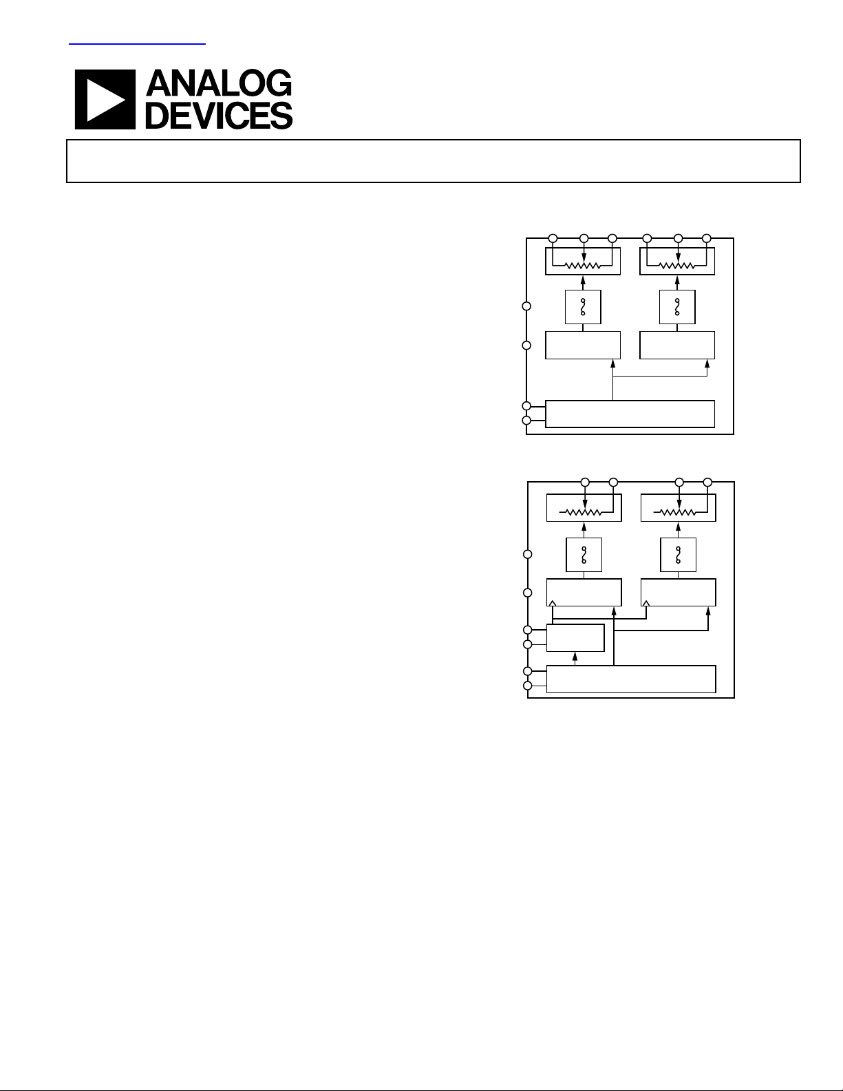
FUNCTIONAL BLOCK DIAGRAMS
RDAC
RDAC
B2
B2
2
C controllers,
V
ND
SDA
SCL
A1
DD
12
REGISTER 1
W1
RDAC
SERIAL INPUT
B1 A2 W2
FUSE
LINKS
REGISTER 2
/
8
REGISTER
Figure 1. AD5172
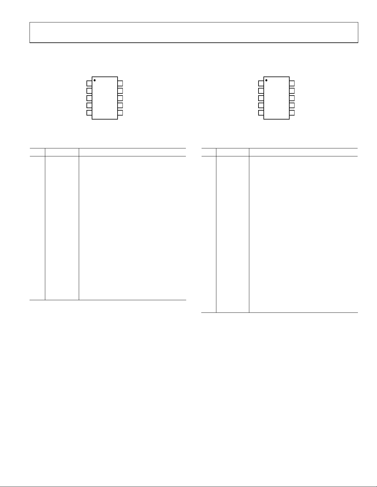
B1 W2
W1
V
ND
AD0
AD1
SDA
SCL
DD
12
RDAC
REGISTER 1
ADDRESS
DECODE
FUSE
LINKS
/
8
SERIAL INPUT
REGISTER
REGISTER 2
Figure 2. AD5173
Unlike traditional OTP digital potentiometers, the AD5172/
AD5173 have a unique temporary OTP overwrite feature that
allows for new adjustments even after a fuse has been blown.
However, the OTP setting is restored during subsequent powerup conditions. This allows users to treat these digital potentiometers as volatile potentiometers with a programmable preset.
For applications that program the AD5172/AD5173 at the
factory, Analog Devices offers device programming software
running on Windows® 2000, NT, and XP operating systems.
This software effectively replaces any external I
thus enhancing the time-to-market of the user’s systems.
1
The terms digital potentiometer, VR, and RDAC are used interchangeably.
One Technology Way, P.O. Box 9106, Norwood, MA 02062-9106, U.S.A.
Tel: 781.329.4700 www.analog.com
Fax: 781.461.3113 © 2005 Analog Devices, Inc. All rights reserved.
04103-0-001
04103-0-002

AD5172/AD5173
TABLE OF CONTENTS
Electrical Characteristics—2.5 kΩ Version................................... 3
Terminal Voltage Operating Range ......................................... 17
Electrical Characteristics—10 kΩ, 50 kΩ, 100 kΩ Versions....... 5
Timing Characteristics—2.5 kΩ, 10 kΩ, 50 kΩ,
100 kΩ Versions ................................................................................ 7
Absolute Maximum Ratings............................................................ 8
Pin Configurations and Function Descriptions ........................... 9
Typical Performance Characteristics ........................................... 10
Test Cir c ui t s .....................................................................................14
Theory of Operation ...................................................................... 15
One-Time Programming (OTP) .............................................. 15
Programming the Variable Resistor and Voltage ................... 15
Programming the Potentiometer Divider............................... 16
ESD Protection ........................................................................... 17
REVISION HISTORY
6/05—Rev. B to Rev. C
Added Footnote 8, Footnote 9, and Footnote 10 to Table 1 .......... 3
Added Footnote 8 to Table 2 .............................................................. 5
Changes to Table 5 and Table 6.......................................................... 9
Changes to Power Supply Considerations Section........................ 17
Changes to I
Added Level Shifting for Different Voltage Operation Section... 24
Updated Outline Dimensions.......................................................... 25
Changes to Ordering Guide............................................................. 25
2
C-Compatible 2-Wire Serial Bus Section................ 23
Power-Up Sequence ................................................................... 17
Power Supply Considerations................................................... 17
Layout Considerations............................................................... 18
Evaluation Software/Hardware..................................................... 19
Software Programming ............................................................. 19
Device Programming................................................................. 20
2
I
C Interface .................................................................................... 21
2
I
C-Compatible 2-Wire Serial Bus........................................... 23
Level Shifting for Different Voltage Operation ...................... 24
Outline Dimensions ....................................................................... 25
Ordering Guide .......................................................................... 25
10/04—Rev. A to Rev. B
Updated Format ................................................................Universal
Changes to Specifications................................................................ 3
Changes to One-Time Programming (OTP) Section ............... 13
Changes to Power Supply Considerations Section.................... 15
Changes to Figure 44 and Figure 45 ............................................ 15
Changes to Figure 46 and Figure 47 ............................................ 16
11/03—Rev. 0 to Rev. A
Changes to Electrical Characteristics—2.5 kΩ............................. 3
Rev. C | Page 2 of 28

AD5172/AD5173
ELECTRICAL CHARACTERISTICS—2.5 kΩ VERSION
VDD = 5 V ± 10% or 3 V ± 10%; VA = VDD; VB = 0 V; –40°C < TB
Table 1.
Parameter Symbol Conditions Min Typ1Max Unit
DC CHARACTERISTICS—RHEOSTAT MODE
Resistor Differential Nonlinearity
Resistor Integral Nonlinearity
Nominal Resistor Tolerance
2
2
3
R-DNL RWB, VA = No connect −2 ±0.1 +2 LSB
R-INL RWB, VA = No connect −6 ±0.75 +6 LSB
∆R
AB
Resistance Temperature Coefficient (∆RAB/RAB)/∆T 35 ppm/°C
RWB (Wiper Resistance) R
WB
DC CHARACTERISTICS—POTENTIOMETER DIVIDER MODE (Specifications Apply to All VRs)
Differential Nonlinearity
Integral Nonlinearity
Voltage Divider Temperature
4
4
DNL −1.5 ±0.1 +1.5 LSB
INL −2 ±0.6 +2 LSB
(ΔV
)/ΔT Code = 0x80 15 ppm/°C
W/VW
Coefficient
Full-Scale Error V
Zero-Scale Error V
WFSE
WZSE
RESISTOR TERMINALS
Voltage Range
Capacitance6 A, B CA, C
Capacitance6 W C
Shutdown Supply Current
Common-Mode Leakage I
5
7
VA, VB, V
B
W
I
A_SD
CM
W
DIGITAL INPUTS AND OUTPUTS
Input Logic High (SDA and SCL)
Input Logic Low (SDA and SCL)
Input Logic High (AD0 and AD1) V
Input Logic Low (AD0 and AD1) V
Input Current I
Input Capacitance
6
8
8
V
IH
V
IL
IH
IL
IL
C
IL
POWER SUPPLIES
Power Supply Range V
OTP Supply Voltage
8, 9
Supply Current I
OTP Supply Current
Power Dissipation
8, 10
11
DD RANGE
V
DD_OTP
DD
I
DD_OTP
P
DISS
Power Supply Sensitivity PSS VDD = 5 V ± 10%, Code = Midscale ±0.02 ±0.08 %/%
< +125°C; unless otherwise noted.
A
TA = 25°C −20 +55 %
Code = 0x00, VDD = 5 V 160 200 Ω
Code = 0xFF −10 −2.5 0 LSB
Code = 0x00 0 2 10 LSB
GND V
f = 1 MHz, Measured to GND,
45 pF
DD
V
Code = 0x80
f = 1 MHz, Measured to GND,
60 pF
Code = 0x80
VDD = 5.5 V 0.01 1 μA
VA = VB = VDD/2 1 nA
VDD = 5 V 0.7 VDD
VDD + 0.5
V
VDD = 5 V −0.5 +0.3 VDDV
VDD = 3 V 2.1 V
VDD = 3 V 0.6 V
VIN = 0 V or 5 V ±1 μA
5 pF
2.7 5.5 V
TA = 25°C 5.25 5.5 V
VIH = 5 V or VIL = 0 V 3.5 6 μA
V
= 5.5 V, TA = 25°C 100 mA
DD_OTP
VIH = 5 V or VIL = 0 V, VDD = 5 V 30 μW
Rev. C | Page 3 of 28

AD5172/AD5173
Parameter Symbol Conditions Min Typ1Max Unit
DYNAMIC CHARACTERISTICS
Bandwidth −3 dB BW_2.5 K Code = 0x80 4.8 MHz
Total Harmonic Distortion THD
VW Settling Time t
Resistor Noise Voltage Density e
1
Typical specifications represent average readings at 25°C and VDD = 5 V.
2
Resistor position nonlinearity error, R-INL, is the deviation from an ideal value measured between the maximum resistance and the minimum resistance wiper
positions. R-DNL measures the relative step change from the ideal between successive tap positions. Parts are guaranteed monotonic.
3
VAB = VDD, Wiper (VW) = no connect.
4
INL and DNL are measured at VW with the RDAC configured as a potentiometer divider similar to a voltage output DAC. VA = VDD and VB = 0 V. DNL specification
limits of ±1 LSB maximum are guaranteed monotonic operating conditions.
5
Resistor Terminals A, B, and W have no limitations on polarity with respect to each other.
6
Guaranteed by design and not subject to production test.
7
Measured at the A terminal. The A terminal is open-circuited in shutdown mode.
8
The minimum voltage requirement on the VIH is 0.7 V × VDD. For example, VIH min = 3.5 V when VDD = 5 V. It is typical for the SCL and SDA resistors to be pulled up to
V
. However, care must be taken to ensure that the minimum VIH is met when the SCL and SDA are driven directly from a low voltage logic controller without pull-
DD
up resistors.
9
Different from operating power supply; power supply for OTP is used one time only.
10
Different from operating current; supply current for OTP lasts approximately 400 ms for one time only.
11
P
is calculated from (IDD × VDD). CMOS logic level inputs result in minimum power dissipation.
DISS
12
All dynamic characteristics use VDD = 5 V.
12
W
S
VA = 1 V rms, VB = 0 V, f = 1 kHz 0.1 %
VA = 5 V, VB = 0 V, ±1 LSB error
B
1 μs
band
N_WB
RWB = 1.25 kΩ, RS = 0 3.2 nV/√Hz
Rev. C | Page 4 of 28

AD5172/AD5173
ELECTRICAL CHARACTERISTICS—10 kΩ, 50 kΩ, 100 kΩ VERSIONS
VDD = 5 V ± 10% or 3 V ± 10%; VA = VDD; VB = 0 V; –40°C < TB
Table 2.
Parameter Symbol Conditions Min Typ1Max Unit
DC CHARACTERISTICS—RHEOSTAT MODE
Resistor Differential Nonlinearity
Resistor Integral Nonlinearity
Nominal Resistor Tolerance
2
2
3
R-DNL RWB, VA = No connect –1 ±0.1 +1 LSB
R-INL RWB, VA = No connect –2.5 ±0.25 +2.5 LSB
ΔR
AB
Resistance Temperature Coefficient (ΔRAB/RAB)/ΔT 35 ppm/°C
RWB (Wiper Resistance) R
WB
DC CHARACTERISTICS—POTENTIOMETER DIVIDER MODE (Specifications Apply to all VRs)
Differential Nonlinearity
Integral Nonlinearity
Voltage Divider Temperature
4
4
DNL –1 ±0.1 +1 LSB
INL –1 ±0.3 +1 LSB
(ΔV
)/ΔT Code = 0x80 15 ppm/°C
W/VW
Coefficient
Full-Scale Error V
Zero-Scale Error V
WFSE
WZSE
RESISTOR TERMINALS
Voltage Range
Capacitance6 A, B CA, C
Capacitance W
Shutdown Supply Current
Common-Mode Leakage I
5
6
7
VA, VB, V
B
C
W
I
A_SD
CM
W
DIGITAL INPUTS AND OUTPUTS
Input Logic High (SDA and SCL)
Input Logic Low (SDA and SCL)
Input Logic High (AD0 and AD1) V
Input Logic Low (AD0 and AD1) V
Input Current I
Input Capacitance
6
8
8
V
IH
V
IL
IH
IL
IL
C
IL
POWER SUPPLIES
Power Supply Range V
OTP Supply Voltage
8, 9
Supply Current I
OTP Supply Current
Power Dissipation
8, 10
11
DD RANGE
V
DD_OTP
DD
I
DD_OTP
P
DISS
Power Supply Sensitivity PSS VDD = +5 V ± 10%, Code = Midscale ±0.02 ±0.08 %/%
< +125°C; unless otherwise noted.
A
TA = 25°C –20 +20 %
Code = 0x00, VDD = 5 V 160 200 Ω
Code = 0xFF –2.5 –1 0 LSB
Code = 0x00 0 1 2.5 LSB
GND V
f = 1 MHz, Measured to GND,
45 pF
DD
V
Code = 0x80
f = 1 MHz, Measured to GND,
60 pF
Code = 0x80
VDD = 5.5 V 0.01 1 μA
VA = VB = VDD/2 1 nA
VDD = 5 V 0.7 VDD V
VDD = 5 V –0.5
+ 0.5 V
DD
+0.3
V
DD
V
VDD = 3 V 2.1 V
VDD = 3 V 0.6 V
VIN = 0 V or 5 V ±1 μA
5 pF
2.7 5.5 V
5.25 5.5 V
VIH = 5 V or VIL = 0 V 3.5 6 μA
V
= 5.5 V, TA = 25°C 100 mA
DD_OTP
VIH = 5 V or VIL = 0 V, VDD = 5 V 30 μW
Rev. C | Page 5 of 28

AD5172/AD5173
Parameter Symbol Conditions Min Typ1Max Unit
DYNAMIC CHARACTERISTICS
Bandwidth –3 dB BW RAB = 10 kΩ, Code = 0x80 600 kHz
R
R
Total Harmonic Distortion THD
VW Settling Time (10 kΩ/50 kΩ/100 kΩ) t
Resistor Noise Voltage Density e
1
Typical specifications represent average readings at 25°C and VDD = 5 V.
2
Resistor position nonlinearity error, R-INL, is the deviation from an ideal value measured between the maximum resistance and the minimum resistance wiper
positions. R-DNL measures the relative step change from the ideal between successive tap positions. Parts are guaranteed monotonic.
3
VAB = VDD, Wiper (VW) = no connect.
4
INL and DNL are measured at VW with the RDAC configured as a potentiometer divider similar to a voltage output DAC. VA = VDD and VB = 0 V. DNL specification
limits of ±1 LSB maximum are guaranteed monotonic operating conditions.
5
Resistor Terminals A, B, and W have no limitations on polarity with respect to each other.
6
Guaranteed by design and not subject to production test.
7
Measured at the A terminal. The A terminal is open-circuited in shutdown mode.
8
The minimum voltage requirement on the VIH is 0.7 V × VDD. For example, VIH min = 3.5 V when VDD = 5 V. It is typical for the SCL and SDA have resistors to be pulled
up to VDD. However, care must be taken to ensure that the minimum VIH is met when the SCL and SDA are driven directly from a low voltage logic controller without
pull-up resistors.
9
Different from operating power supply, power supply OTP is used one time only.
10
Different from operating current, supply current for OTP lasts approximately 400 ms for one time only.
11
P
is calculated from (IDD × VDD). CMOS logic level inputs result in minimum power dissipation.
DISS
12
All dynamic characteristics use VDD = 5 V.
12
= 50 kΩ, Code = 0x80 100 kHz
AB
= 100 kΩ, Code = 0x80 40 kHz
AB
W
S
VA = 1 V rms, VB = 0 V, f = 1 kHz,
= 10 kΩ
R
AB
VA = 5 V, VB = 0 V, ±1 LSB error
B
0.1 %
2 μs
band
N_WB
RWB = 5 kΩ, RS = 0 9 nV/√Hz
Rev. C | Page 6 of 28

AD5172/AD5173
TIMING CHARACTERISTICS—2.5 kΩ, 10 kΩ, 50 kΩ, 100 kΩ VERSIONS
VDD = 5 V ± 10% or 3 V ± 10%; VA = VDD; VB = 0 V; –40°C < TB
Table 3.
Parameter Symbol Conditions Min Typ Max Unit
I2C INTERFACE TIMING CHARACTERISTICS
SCL Clock Frequency f
t
Bus Free Time Between Stop and Start t
BUF
t
Hold Time (Repeated Start) t
HD;STA
t
Low Period of SCL Clock t
LOW
t
High Period of SCL Clock t
HIGH
t
Setup Time for Repeated Start
SU;STA
1
SCL
1
2
3
4
t
5
Condition
t
Data Hold Time
HD;DAT
t
Data Setup Time t
SU;DAT
tF Fall Time of Both SDA and SCL Signals t
tR Rise Time of Both SDA and SCL Signals t
t
Setup Time for Stop Condition t
SU;STO
1
See the timing diagrams (Figure 51 to Figure 55) for locations of measured values.
2
The maximum t
HD;DAT
2
has only to be met if the device does not stretch the low period (t
t
6
7
8
9
10
< +125°C; unless otherwise noted.
A
400 kHz
1.3 μs
After this period, the first clock pulse
0.6 μs
is generated.
1.3 μs
0.6 μs
0.6 μs
0.9 μs
100 ns
300 ns
300 ns
0.6 μs
) of the SCL signal.
LOW
Rev. C | Page 7 of 28

AD5172/AD5173
ABSOLUTE MAXIMUM RATINGS
TA = 25°C, unless otherwise noted.
Table 4.
Parameter Rating
VDD to GND –0.3 V to +7 V
VA, VB, VW to GND V
Terminal Current, Ax to Bx, Ax to Wx, Bx to
1
Wx
DD
Pulsed ±20 mA
Continuous ±5 mA
Digital Inputs and Output Voltage to GND 0 V to 7 V
Operating Temperature Range –40°C to +125°C
Maximum Junction Temperature (T
) 150°C
JMAX
Storage Temperature –65°C to +150°C
Lead Temperature (Soldering, 10 sec) 300°C
Thermal Resistance2 θJA: MSOP-10 230°C/W
1
Maximum terminal current is bound by the maximum current handling of
the switches, maximum power dissipation of the package, and maximum
applied voltage across any two of the A, B, and W terminals at a given
resistance.
2
Package power dissipation = (TJ max – TA)/θJA.
Stresses above those listed under Absolute Maximum Ratings
may cause permanent damage to the device. This is a stress
rating only; functional operation of the device at these or any
other conditions above those indicated in the operational
section of this specification is not implied. Exposure to absolute
maximum rating conditions for extended periods may affect
device reliability.
ESD CAUTION
ESD (electrostatic discharge) sensitive device. Electrostatic charges as high as 4000 V readily accumulate on the
human body and test equipment and can discharge without detection. Although this product features
proprietary ESD protection circuitry, permanent damage may occur on devices subjected to high energy
electrostatic discharges. Therefore, proper ESD precautions are recommended to avoid performance
degradation or loss of functionality.
Rev. C | Page 8 of 28
AD5172/AD5173
PIN CONFIGURATIONS AND FUNCTION DESCRIPTIONS
W2
1
B1
2
A1
3
AD5172
TOP VIEW
4
5
DD
10
W1
9
B2
8
A2
7
SDAGND
6
SCLV
04103-0-045
Figure 3. AD5172 Pin Configuration
Table 5. AD5172 Pin Function Descriptions
Pin Mnemonic Description
1 B1 B1 Terminal. GND ≤ VB1 ≤ VDD.
2 A1 A1 Terminal. GND ≤ VA1 ≤ VDD.
3 W2 W2 Terminal. GND ≤ VW2 ≤ VDD.
4 GND Digital Ground.
5 V
DD
Positive Power Supply. Specified for
operation from 2.7 V to 5.5 V. For OTP
programming, VDD needs to be a minimum
of 5.25 V but no more than 5.5 V and have a
100 mA driving capability.
6 SCL
Serial Clock Input. Positive-edge triggered.
Requires a pull-up resistor. If it is driven
direct from a logic controller without the
pull-up resistor, ensure that V
.
DD
7 SDA
0.7 V × V
Serial Data Input/Output. Requires a pull-
up resistor. If it is driven direct from a logic
controller without the pull-up resistor,
ensure that V
min is 0.7 V × VDD.
IH
8 A2 A2 Terminal. GND ≤ VA2 ≤ VDD.
9 B2 B2 Terminal. GND ≤ VB2 ≤ VDD.
10 W1 W1 Terminal. GND ≤ VW1 ≤ VDD.
min is
IH
AD0
W2
1
B1
2
3
AD5173
TOP VIEW
4
5
DD
10
W1
9
B2
8
AD1
7
SDAGND
6
SCLV
04103-0-046
Figure 4. AD5173 Pin Configuration
Table 6. AD5173 Pin Function Descriptions
Pin Mnemonic Description
1 B1 B1 Terminal. GND ≤ VB1 ≤ VDD.
2 AD0
Programmable Address Bit 0 for Multiple
Package Decoding.
3 W2 W2 Terminal. GND ≤ VW2 ≤ VDD.
4 GND Digital Ground.
5 V
DD
Positive Power Supply. Specified for
operation from 2.7 V to 5.5 V. For OTP
programming, VDD needs to be a minimum
of 5.25 V but no more than 5.5 V and have a
100 mA driving capability.
6 SCL
Serial Clock Input. Positive-edge triggered.
Requires a pull-up resistor. If it is driven
direct from a logic controller without the
pull-up resistor, ensure that V
7 SDA
0.7 V × V
Serial Data Input/Output. Requires a pull-
.
DD
up resistor. If it is driven direct from a logic
controller without the pull-up resistor,
8 AD1
ensure that V
Programmable Address Bit 1 for Multiple
min is 0.7 V × VDD.
IH
Package Decoding.
9 B2 B2 Terminal. GND ≤ VB2 ≤ VDD.
10 W1 W1 Terminal. GND ≤ VW1 ≤ VDD.
min is
IH
Rev. C | Page 9 of 28

AD5172/AD5173
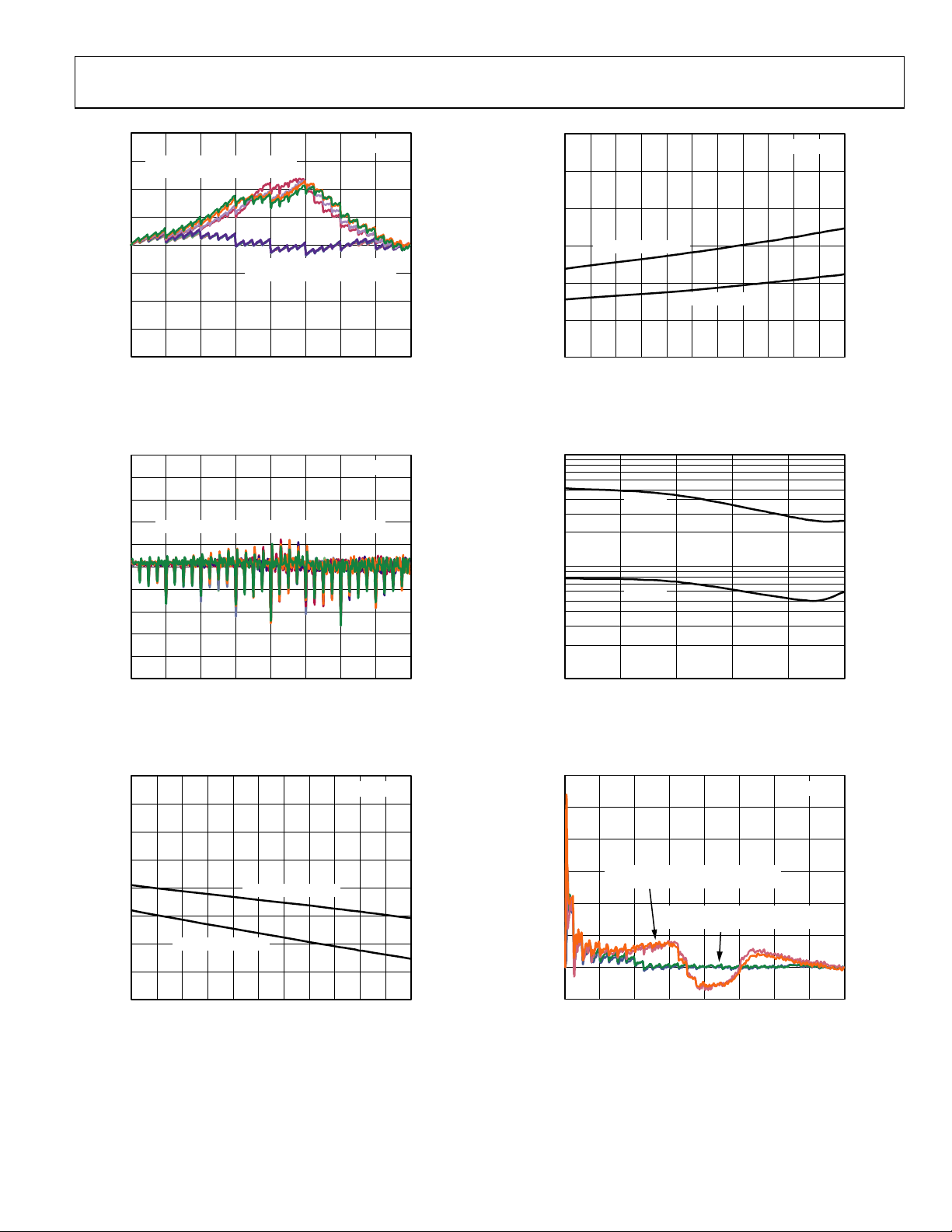
TYPICAL PERFORMANCE CHARACTERISTICS
2.0
1.5
1.0
0.5
0
–0.5
–1.0
RHEOSTAT MODE INL (LSB)
–1.5
–2.0
VDD = 2.7V
Figure 5. R-INL vs. Code vs. Supply Voltages
0.5
0.4
0.3
0.2
0.1
0
–0.1
–0.2
RHEOSTAT MODE DNL (LSB)
–0.3
–0.4
–0.5
Figure 6. R-DNL vs. Code vs. Supply Voltages
0.5
0.4
0.3
0.2
0.1
0
–0.1
–0.2
–0.3
POTENTIOMETER MODE INL (LSB)
–0.4
–0.5
Figure 7. INL vs. Code vs. Temperature
VDD = 5.5V
1289632 640 160 192 224 256
CODE (DECIMAL)
VDD = 2.7V
VDD = 5.5V
1289632 640 160 192 224 256
CODE (DECIMAL)
VDD = 5.5V
T
= –40°C, +25°C, +85°C, +125°C
A
VDD = 2.7V
T
= –40°C, +25°C, +85°C, +125°C
A
1289632 640 160 192 224 256
CODE (DECIMAL)
TA = 25°C
R
= 10kΩ
AB
TA = 25°C
R
= 10kΩ
AB
RAB = 10kΩ
04103-0-003
04103-0-004
04103-0-005
0.5
0.4
0.3
0.2
0.1
0
–0.1
–0.2
–0.3
POTENTIOMETER MODE DNL (LSB)
–0.4
–0.5
VDD = 2.7V; TA = –40°C, +25°C, +85°C, +125°C
1289632 640 160 192 224 256
CODE (DECIMAL)
RAB = 10kΩ
04103-0-006
Figure 8. DNL vs. Code vs. Temperature
1.0
0.8
0.6
0.4
0.2
0
–0.2
–0.4
–0.6
POTENTIOMETER MODE INL (LSB)
–0.8
–1.0
VDD = 2.7V
1289632 640 160 192 224 256
CODE (DECIMAL)
VDD = 5.5V
TA = 25°C
R
= 10kΩ
AB
04103-0-007
Figure 9. INL vs. Code vs. Supply Voltages
0.5
0.4
0.3
0.2
0.1
0
–0.1
–0.2
–0.3
POTENTIOMETER MODE DNL (LSB)
–0.4
–0.5
VDD = 2.7V
VDD = 5.5V
1289632 640 160 192 224 256
CODE (DECIMAL)
TA = 25°C
R
= 10kΩ
AB
04103-0-008
Figure 10. DNL vs. Code vs. Supply Voltages
Rev. C | Page 10 of 28
AD5172/AD5173
2.0
VDD = 2.7V
1.5
T
= –40°C, +25°C, +85°C, +125°C
A
1.0
0.5
RAB = 10kΩ
4.50
RAB = 10kΩ
3.75
3.00
0
–0.5
–1.0
RHEOSTAT MODE INL (LSB)
–1.5
–2.0
Figure 11. R-INL vs. Code vs. Temperature
0.5
0.4
0.3
0.2
VDD = 2.7V, 5.5V; TA = –40°C, +25°C, +85°C, +125°C
0.1
0
–0.1
–0.2
RHEOSTAT MODE DNL (LSB)
–0.3
–0.4
–0.5
Figure 12. R-DNL vs. Code vs. Temperature
2.0
1.5
1.0
0.5
0
–0.5
–1.0
FSE, FULL-SCALE ERROR (LSB)
–1.5
VDD = 2.7V, VA = 2.7V
VDD = 5.5V
T
= –40°C, +25°C, +85°C, +125°C
A
1289632 640 160 192 224 256
CODE (DECIMAL)
1289632 640 160 192 224 256
CODE (DECIMAL)
VDD = 5.5V, VA = 5.0V
RAB = 10kΩ
RAB = 10kΩ
04103-0-009
04103-0-010
2.25
1.50
ZSE, ZERO-SCALE ERROR (LSB)
0.75
VDD = 2.7V, VA = 2.7V
VDD = 5.5V, VA = 5.0V
0
–40 –25 –10 5 20 35 50 65 80 95 110 125
TEMPERATURE (°C)
Figure 14. Zero-Scale Error vs. Temperature
10
A)
μ
1
, SUPPLY CURRENT (
DD
I
0.1
–40 –7 26 59 92 125
VDD = 5V
VDD = 3V
TEMPERATURE (°C)
Figure 15. Supply Current vs. Temperature
120
100
80
60
40
20
RHEOSTAT MODE TEMPCO (ppm/°C)
0
VDD = 2.7V
T
= –40°C TO +85°C, –40°C TO +125°C
A
VDD = 5.5V
T
= –40°C TO +85°C, –40°C TO +125°C
A
RAB = 10kΩ
04103-0-012
04103-0-013
–2.0
–40 –25 –10 5 20 35 50 65 80 95 110 125
TEMPERATURE (°C)
Figure 13. Full-Scale Error vs. Temperature
04103-0-011
Rev. C | Page 11 of 28
–20
CODE (DECIMAL)
Figure 16. Rheostat Mode Tempco ΔR
1289632 640 160 192 224 256
/ΔT vs. Code
WB
04103-0-014

AD5172/AD5173
50
40
30
VDD = 2.7V
T
20
10
0
–10
–20
POTENTIOMETER MODE TEMPCO (ppm/°C)
–30
Figure 17. AD5172 Potentiometer Mode Tempco ΔV
0
–6
–12
–18
–24
–30
GAIN (dB)
–36
–42
–48
–54
–60
10k 1M100k 10M
0
–6
–12
–18
–24
–30
GAIN (dB)
–36
–42
–48
–54
–60
1k 100k10k 1M
= –40°C TO +85°C, –40°C TO +125°C
A
VDD = 5.5V
T
= –40°C TO +85°C, –40°C TO +125°C
A
1289632 640 160 192 224 256
CODE (DECIMAL)
0x80
0x40
0x20
0x10
0x08
0x04
0x010x02
FREQUENCY (Hz)
Figure 18. Gain vs. Frequency vs. Code, R
0x80
0x40
0x20
0x10
0x08
0x04
0x02
0x01
FREQUENCY (Hz)
Figure 19. Gain vs. Frequency vs. Code, R
RAB = 10kΩ
/ΔT vs. Code
WB
= 2.5 kΩ
AB
= 10 kΩ
AB
04103-0-047
04103-0-048
04103-0-049
0
–6
–12
–18
–24
–30
GAIN (dB)
–36
–42
–48
–54
–60
1k 100k10k 1M
0x80
0x40
0x20
0x10
0x08
0x04
0x02
0x01
FREQUENCY (Hz)
Figure 20. Gain vs. Frequency vs. Code, R
0
–6
–12
–18
–24
–30
GAIN (dB)
–36
–42
–48
–54
–60
1k 100k10k 1M
Figure 21. Gain vs. Frequency vs. Code, R
0x80
0x40
0x20
0x10
0x08
0x04
0x02
0x01
FREQUENCY (Hz)
AB
0
–6
–12
–18
–24
–30
GAIN (dB)
–36
–42
–48
–54
–60
100kΩ
60kHz
50kΩ
120kHz
10kΩ
570kHz
2.5kΩ
2.2MHz
10k1k 100k 1M 10M
FREQUENCY (Hz)
Figure 22. –3 dB Bandwidth @ Code = 0x80
= 50 kΩ
AB
= 100 kΩ
04103-0-050
04103-0-051
04103-0-052
Rev. C | Page 12 of 28

AD5172/AD5173
10
TA = 25°C
1
0.1
, SUPPLY CURRENT (mA)
DD
I
0.01
0 0.5 1.0 1.5 2.0 2.5 3.0 3.5 4.0 4.5 5.0
VDD = 2.7V
DIGITAL INPUT VOLTAGE (V)
Figure 23. I
VDD = 5.5V
vs. Input Voltage
DD
V
W
SCL
04103-0-057
V
W2
V
W1
04103-0-056
Figure 26. Analog Crosstalk
V
W
04103-0-053
Figure 24. Digital Feedthrough
V
W2
V
W1
04103-0-054
Figure 25. Digital Crosstalk
Figure 27. Midscale Glitch, Code 0x80 to Code 0x7F
V
W
SCL
Figure 28. Large Signal Settling Time
04103-0-058
04103-0-055
Rev. C | Page 13 of 28

AD5172/AD5173
TEST CIRCUITS
Figure 29 to Figure 36 illustrate the test circuits that define the
test conditions used in the product specification tables.
DUT
A
V+
W
B
Figure 29. Potentiometer Divider Nonlinearity Error (INL, DNL)
NO CONNECT
DUT
A
W
B
Figure 30. Resistor Position Nonlinearity Error
(Rheostat Operation; R-INL, R-DNL)
DUT
V
MS2
A
B
V
W
W
Figure 31. Wiper Resistance
V
A
DUT
V
DD
A
V+
W
B
Figure 32. Power Supply Sensitivity (PSS, PSSR)
V+ = V
1LSB = V+/2
V
MS
V
MS
IW= VDD/R
V
RW= [V
MS1
10%
V+ = V
DD
PSRR (dB) = 20 LOG
PSS (%/%) =
V
MS
DD
I
W
NOMINAL
MS1
ΔV
ΔV
N
04103-0-015
04103-0-016
– V
%
MS
%
DD
]/I
MS2
ΔV
( )
ΔV
W
04103-0-017
MS
DD
04103-0-018
OFFSET
GND
A
DUT
V
IN
2.5V
B
+5V
W
AD8610
–5V
V
OUT
04103-0-019
Figure 33. Test Circuit for Gain vs. Frequency
0.1V
RSW=
I
DUT
B
W
I
SW
GND TO V
SW
CODE = 0x00
DD
0.1V
04103-0-020
Figure 34. Incremental On Resistance
NC
DUT
V
DD
GND
NC
I
A
CM
W
B
V
CM
04103-0-021
Figure 35. Common-Mode Leakage Current
A1
V
RDAC1
W1
N/C
V
IN
CTA = 20 log[V
V
B1
DD
SS
OUT/VIN
A2
RDAC2
W2
B2
]
V
OUT
04103-0-022
Figure 36. Analog Crosstalk
Rev. C | Page 14 of 28

AD5172/AD5173
THEORY OF OPERATION
SCL
SDA
2
I
C INTERFACE
COMPARATOR
ONE-TIME
PROGRAM/TEST
CONTROL BLOCK
Figure 37. Detailed Functional Block Diagram
The AD5172/AD5173 are 256-position, digitally controlled
variable resistors (VRs) that employ fuse link technology to
achieve memory retention of resistance setting.
An internal power-on preset places the wiper at midscale
during power-on. If the OTP function has been activated, the
device powers up at the user-defined permanent setting.
ONE-TIME PROGRAMMING (OTP)
Prior to OTP activation, the AD5172/AD5173 presets to midscale during initial power-on. After the wiper is set to the
desired position, the resistance can be permanently set by
programming the T bit high, the proper coding (see
Tabl e 8), and one-time V
. The fuse link technology of the
DD_OTP
AD517x family of digital potentiometers requires V
between 5.25 V and 5.5 V to blow the fuses to achieve a given
nonvolatile setting. Conversely, V
can be 2.7 V to 5.5 V
DD
during operation. As a result, system supply that is lower than
5.25 V requires an external supply for one-time programming.
The user is allowed only one attempt to blow the fuses. If the
user fails to blow the fuses during this attempt, the structure of
the fuses can change such that they might never be blown,
regardless of the energy applied at subsequent events. For
details, see the
Power Supply Considerations section.
The device control circuit has two validation bits, E1 and E0,
that can be read back to check the programming status (see
Tabl e 9). Users should always read back the validation bits to
ensure that the fuses are properly blown. After the fuses have
been blown, all fuse latches are enabled upon subsequent
power-on; therefore, the output corresponds to the stored
setting.
Figure 37 shows a detailed functional block diagram.
Tabl e 7 and
to be
DD_OTP
A
W
B
04103-0-026
DAC
REG.
FUSES
EN
MUX
FUSE
REG.
DECODER
PROGRAMMING THE VARIABLE RESISTOR AND
VOLTAGE
Rheostat Operation
The nominal resistance of the RDAC between Terminal A and
Terminal B is available in 2.5 kΩ, 10 kΩ, 50 kΩ, and 100 kΩ.
The nominal resistance (R
accessed by the wiper terminal, and the B terminal contact.
The 8-bit data in the RDAC latch is decoded to select one of the
256 possible settings.
A
W
B
Figure 38. Rheostat Mode Configuration
Assuming a 10 kΩ part is used, the wiper’s first connection
starts at the B terminal for data 0x00. Because there is a 50 Ω
wiper contact resistance, such a connection yields a minimum
of 100 Ω (2 × 50 Ω) resistance between Terminal W and
Terminal B. The second connection is the first tap point,
which corresponds to 139 Ω (R
39 Ω + 2 × 50 Ω) for data 0x01. The third connection is the
next tap point, representing 178 Ω (2 × 39 Ω + 2 × 50 Ω) for
data 0x02, and so on. Each LSB data value increase moves the
wiper up the resistor ladder until the last tap point is reached at
10,100 Ω (R
+ 2 × RW).
AB
) of the VR has 256 contact points
AB
A
W
B
= RAB/256 + 2 × RW =
WB
A
B
W
04103-0-027
Rev. C | Page 15 of 28

AD5172/AD5173
−
A
R
S
D7
D6
D5
D4
D3
D2
D1
D0
RDAC
LATCH
AND
DECODER
Figure 39. AD5172/AD5173 Equivalent RDAC Circuit
The general equation that determines the digitally programmed
output resistance between W and B is
D
DR ×+×= 2
)(
128
where D is the decimal equivalent of the binary code loaded in
the 8-bit RDAC register, R
is the wiper resistance contributed by the on resistance of
R
W
the internal switch.
In summary, if R
= 10 kΩ and the A terminal is open-circuited,
AB
the output resistance R
shown in
Tabl e 7.
Table 7. Codes and Corresponding RWB Resistance
D (Dec) RWB (Ω) Output State
255 9,961 Full scale (RAB – 1 LSB + RW)
128 5,060 Midscale
1 139 1 LSB
0 100 Zero scale (wiper contact resistance)
Note that in the zero-scale condition, a finite wiper resistance of
100 Ω is present. Care should be taken to limit the current flow
between W and B in this state to a maximum pulse current of
no more than 20 mA. Otherwise, degradation or possible
destruction of the internal switch contact can occur.
Similar to the mechanical potentiometer, the resistance of the
RDAC between the Wiper W and Terminal A also produces a
digitally controlled complementary resistance, R
terminals are used, the B terminal can be opened. Setting the
resistance value for R
and decreases as the data loaded in the latch increases in value.
The general equation for this operation is
DR ×+×= 2
–256
)(
128
R
S
R
S
W
R
S
B
04103-0-028
(1)
WABWB RR
is the end-to-end resistance, and
AB
is set for the RDAC latch codes, as
WB
. When these
WA
starts at a maximum value of resistance
WA
D
(2)
WABWA RR
= 10 kΩ and the B terminal open-circuited, the
For R
AB
following output resistance R
as shown in
Tabl e 8 .
is set for the RDAC latch codes,
WA
Table 8. Codes and Corresponding RWA Resistance
D (Dec) RWA (Ω) Output State
255 139 Full scale
128 5,060 Midscale
1 9,961 1 LSB
0 10,060 Zero scale
Typical device-to-device matching is process-lot dependent
and may vary up to ±30%. Because the resistance element
is processed using thin film technology, the change in R
AB
with
temperature has a very low 35 ppm/°C temperature coefficient.
PROGRAMMING THE POTENTIOMETER DIVIDER
Voltage Output Operation
The digital potentiometer easily generates a voltage divider at
wiper to B and wiper to A proportional to the input voltage at
A to B. Unlike the polarity of V
positive, voltage across A to B, W to A, and W to B can be at
either polarity.
V
I
Figure 40. Potentiometer Mode Configuration
If ignoring the effect of the wiper resistance for approximation,
connecting the A terminal to 5 V and the B terminal to ground
produces an output voltage at the wiper to B starting at 0 V up
to 1 LSB less than 5 V. Each LSB of voltage is equal to the
voltage applied across Terminal A and Terminal B divided by
the 256 positions of the potentiometer divider. The general
equation defining the output voltage at V
ground for any valid input voltage applied to Terminal A and
Terminal B is
W
256
D
DV
)(
256
V
+=
A
For a more accurate calculation, which includes the effect of
wiper resistance, V
DV
)( +=
W
can be found as
W
DR
)(
WB
V
A
R
AB
Operation of the digital potentiometer in the divider mode
results in a more accurate operation over temperature. Unlike
rheostat mode, the output voltage is dependent mainly on the
ratio of the internal resistors R
values. Thus, the temperature drift reduces to 15 ppm/°C.
to GND, which must be
DD
A
W
V
O
B
04103-0-029
with respect to
W
D
(3)
V
B
256
DR
)(
WA
V
(4)
R
WA
B
AB
and RWB and not the absolute
Rev. C | Page 16 of 28

AD5172/AD5173
3
ESD PROTECTION
All digital inputs—SDA, SCL, AD0, and AD1—are protected
with a series input resistor and parallel Zener ESD structures, as
shown in
Figure 41 and Figure 42.
340Ω
LOGIC
GND
Figure 41. ESD Protection of Digital Pins
A,B,W
GND
Figure 42. ESD Protection of Resistor Terminals
04103-0-030
04103-0-031
TERMINAL VOLTAGE OPERATING RANGE
The AD5172/AD5173 VDD to GND power supply defines the
boundary conditions for proper 3-terminal digital potentiometer operation. Supply signals present on Terminals A, B, and
W that exceed V
biased diodes (see
Figure 43. Maximum Terminal Voltages Set by V
or GND are clamped by the internal forward-
DD
Figure 43).
V
DD
A
W
B
GND
04103-0-032
and GND
DD
POWER-UP SEQUENCE
Because the ESD protection diodes limit the voltage compliance
at Terminals A, B, and W (see
power V
/GND before applying any voltage to Terminals A, B,
DD
and W. Otherwise, the diode is forward biased such that V
powered unintentionally and may affect the rest of the user’s
circuit. The ideal power-up sequence is GND, V
inputs, and then V
V
B, V
, and the digital inputs is not important as long as they
B
W
are powered after V
A/VB
DD
/GND.
Figure 43), it is important to
, the digital
DD
/V
B
. The relative order of powering VA,
W
DD
is
POWER SUPPLY CONSIDERATIONS
To minimize the package pin count, both the one-time programming and normal operating voltage supplies are applied to
the same V
employ fuse link technology that requires 5.25 V to 5.5 V to
blow the internal fuses to achieve a given setting, but normal
V
can be 2.7 V to 5.5 V. Such dual-voltage requirements need
DD
isolation between the supplies if V
V
DD_OTP
regulator or rack-mount power supply) must be rated at 5.25 V
to 5.5 V and must be able to provide a 100 mA transient current
for 400 ms for successful one-time programming. Once
programming is completed, the V
removed to allow normal operation at 2.7 V to 5.5 V and the
device consumes only microamps of current.
the simplest implementation to meet the dual-voltage
requirement with a jumper. This approach saves one voltage
supply, but draws additional current and requires manual
configuration.
An alternate approach in 3.5 V to 5.25 V systems adds a signal
diode between the system supply and the OTP supply for
isolation, as shown in
removed once OTP is completed.
terminal of the device. The AD5172/AD5173
DD
is lower than the required
DD
. The fuse programming supply (either an on-board
supply must be
DD_OTP
Figure 44 shows
5.5V
R1 50kΩ
R2
250kΩ
5.5V
.5V–5.25V
Figure 45. Isolate 5.5 V OTP Supply from 3.5 V to 5.25 V
CONNECT J1 HERE
FOR OTP
C1
10μFC21nF
5V
CONNECT J1 HERE
AFTER OTP
V
DD
AD5172/
AD5173
Figure 44. Power Supply Requirements
Figure 45. The V
APPLY FOR OTP ONLY
D1
C1
10μFC21nF
supply must be
DD_ OTP
V
DD
AD5172/
AD5173
Normal Operating Supply
04103-0-033
04103-0-034
Rev. C | Page 17 of 28
AD5172/AD5173
Y
5.5V
R1
10kΩ
2.7V
Figure 46. Isolate 5.5 V OTP Supply from 2.7 V Normal Operating Supply.
APPLY FOR OTP ONL
C1
P2
10μFC21nF
P1
P1 = P2 = FDV302P, NDS0610
V
DD
AD5172/
AD5173
04103-0-035
For users who operate their systems at 2.7 V, use of the bidirectional, low threshold P-channel MOSFETs is recommended for
the supply’s isolation. As shown in
Figure 46, this assumes that
the 2.7 V system voltage is applied first, and that the P1 and P2
gates are pulled to ground, thus turning on P1 and subsequently
P2. As a result, V
of the AD5172/AD5173 approaches 2.7 V.
DD
When the AD5172/AD5173 setting is found, the factory tester
applies the V
to both the VDD and the MOSFET gates, thus
DD_OTP
turning P1 and P2 off. The OTP command should be executed
at this time to program the AD5172/AD5173 while the 2.7 V
source is protected. Once the OTP is completed, the tester
withdraws the V
and the AD5172/AD5173’s setting is
DD_OTP
fixed permanently.
The AD5172/AD5173 achieve the OTP function by blowing
internal fuses. Users should always apply the 5.25 V to 5.5 V
one-time program voltage requirement at the first fuse programming attempt. Failure to comply with this requirement
may lead to the change of fuse structures, rendering
programming inoperable.
Care should be taken when SCL and SDA are driven from a low
voltage logic controller. Users must ensure that the logic high
level is between 0.7 V × V
and VDD + 0.5 V.
DD
Poor PCB layout introduces parasitics that can affect fuse
programming. Therefore, it is recommended to add a 1 μF to
10 μF tantalum capacitor in parallel with a 1 nF ceramic capacitor
as close as possible to the V
pin. The type and value chosen
DD
for both capacitors are important. This combination of capacitor
values provides both a fast response and larger supply current
handling with minimum supply droop during transients. As a
result, these capacitors increase the OTP programming success
by not inhibiting the proper energy needed to blow the internal
fuses. Additionally, C1
minimizes transient disturbance and low
frequency ripple, while C2 reduces high frequency noise during
normal operation.
LAYOUT CONSIDERATIONS
In PCB layout, it is a good practice to employ compact, minimum lead length design. The leads to the inputs should be as
direct as possible with a minimum conductor length. Ground
paths should have low resistance and low inductance.
Note that the digital ground should also be joined remotely to
the analog ground at one point to minimize the ground bounce.
V
DD
+
C1
10μFC21nF
V
DD
AD5172
GND
04103-0-036
Figure 47. Power Supply Bypassing
Rev. C | Page 18 of 28

AD5172/AD5173
EVALUATION SOFTWARE/HARDWARE
Figure 48. AD5172/AD5173 Computer Software Interface
There are two ways of controlling the AD5172/AD5173. Users
can either program the devices with computer software or with
external I
2
C controllers.
SOFTWARE PROGRAMMING
Due to the advantages of the one-time programmable feature,
consider programming the device in the factory before shipping
the final product to end users. ADI offers device programming
software that can be implemented in the factory on PCs running Windows® 95 or later. As a result, external controllers are
not required, which significantly reduces development time.
The program is an executable file that does not require
knowledge of programming languages or programming
skills, and it is easy to set up and to use.
software interface. The software can be downloaded from
www.analog.com.
Figure 48 shows the
04103-0-060
The AD5172/AD5173 start at midscale after power-up, prior to
OTP programming. To increment or decrement the resistance,
move the scrollbars on the left. To write any specific value, use
the bit pattern in the upper screen and click Run. The format of
writing data to the device is shown in
Tabl e 9. Once the desired
setting is found, click Program Permanent to blow the internal
fuse links.
To read the validation bits and data out from the device, click
Read. The format of the read bits is shown in
Table 1 0.
Rev. C | Page 19 of 28

AD5172/AD5173
DEVICE PROGRAMMING
To apply the device programming software in the factory, users
must modify a parallel port cable and configure Pins 2, 3, 15,
and 25 for SDA_write, SCL, SDA_read, and DGND, respectively,
for the control signals (see
the PCB of the AD5172/AD5173 as shown in
SCL and SDA pads allow pogo pins to be inserted so that
signals can be communicated through the parallel port for the
programming.
Figure 49. Parallel Port Connection
(Pin 2 = SDA_write, Pin 3 = SCL, Pin 15 = SDA_read, and Pin 25 = DGND)
Figure 49). Users should also lay out
Figure 50. The
13
25
12
24
11
23
10
22
9
21
8
20
7
19
6
18
5
17
4
16
3
15
2
14
1
100Ω
R2
100Ω
100Ω
R3
R1
READ
WRITE
SCL
SDA
04103-0-037
AD5172 AD5173
W1
B2
A2
SDA
SCL
AD0
W2
GND
V
B1
DD
W2
GND
V
B1
A1
DD
Figure 50. Recommended AD5172/AD5173 PCB Layout
W1
B2
AD1
SDA
SCL
04103-0-038
Rev. C | Page 20 of 28
AD5172/AD5173
I2C INTERFACE
Tabl e 9 and Tab l e 1 0 use the following codes:
S = Start condition.
P = Stop condition.
A = Acknowledge.
AD0, AD1 = Package pin programmable address bits.
X = Don’t care.
W
= Write.
R = Read.
A0 = RDAC subaddress select bit.
T = OTP Programming Bit. Logic 1 programs the wiper
permanently.
OW = Overwrite the fuse setting and program the digital
potentiometer to a different setting. Upon power-up, the digital
potentiometer is preset to either midscale or fuse setting,
depending on whether or not the fuse link has been blown.
D7, D6, D5, D4, D3, D2, D1, D0 = Data bits.
E1, E0 = OTP Validation Bits.
0, 0 = Ready to program.
1, 0 = Fatal error. Some fuses not blown. Do not retry. Discard
this unit.
SD = Shutdown connects wiper to B terminal and open circuits
the A terminal. It does not change contents of wiper register.
1, 1 = Programmed successfully. No further adjustments are
possible.
Table 9. Write Mode
AD5172
W
S 0 1 0 1 1 1 1
Slave Address Byte Instruction Byte Data Byte
A A0 SD T 0 OW X X X A D7 D6 D5 D4 D3 D2 D1 D0 A P
AD5173
W
S 0 1 0 1 1 AD1 AD0
Slave Address Byte Instruction Byte Data Byte
A A0 SD T 0 OW X X X A D7 D6 D5 D4 D3 D2 D1 D0 A P
Table 10. Read Mode
AD5172
S 0 1 0 1 1 1 1 R A D7 D6 D5 D4 D3 D2 D1 D0 A E1 E0 X X X X X X A P
Slave Address Byte Instruction Byte Data Byte
AD5173
S 0 1 0 1 1 AD1 AD0 R A D7 D6 D5 D4 D3 D2 D1 D0 A E1 E0 X X X X X X A P
Slave Address Byte Instruction Byte Data Byte
Rev. C | Page 21 of 28

AD5172/AD5173
t
2
t
5
10
04103-0-039
P
SCL
SDA
t
2
t
1
PS
t
8
t
3
t
8
t
6
t
9
Figure 51. I
t
9
t
4
2
C Interface Detailed Timing Diagram
t
7
S
t
START BY
MASTER
SCL
SDA
1
01
01111
FRAME 1
SLAVE ADDRESS BYTE
19
R/W A0 SD 0 OW X X X
ACK BY
AD5172
T
FRAME 2
INSTRUCTION BYTE
19
D7 D6 D5 D4 D3
ACK BY
AD5172
FRAME 3
DATA BYTE
D2 D1 D0
9
ACK BY
AD5172
STOP BY
MASTER
04103-0-040
Figure 52. Writing to the RDAC Register—AD5172
START BY
MASTER
SCL
SDA
1
01
0 1 1 AD1 AD0
FRAME 1
SLAVE ADDRESS BYTE
19
R/W A0 SD 0 OW X X X
ACK BY
AD5173
T
FRAME 2
INSTRUCTION BYTE
19
D7 D6 D5 D4 D3
ACK BY
AD5173
FRAME 3
DATA BYTE
D2 D1 D0
9
ACK BY
AD5173
STOP BY
MASTER
04103-0-041
Figure 53. Writing to the RDAC Register—AD5173
START BY
MASTER
SCL
SDA
1
01
01111
FRAME 1
SLAVE ADDRESS BYTE
19
R/W D7 D6 D4 D3 D2 D1 D0
ACK BY
AD5172
D5
FRAME 2
INSTRUCTION BYTE
19
E1 E0 X X X
ACK BY
MASTER
FRAME 3
DATA BYTE
XXX
9
NO ACK
BY MASTER
STOP BY
MASTER
04103-0-042
Figure 54. Reading Data from a Previously Selected RDAC Register in Write Mode—AD5172
START BY
MASTER
SCL
SDA
1
01
0 1 1 AD1 AD0
FRAME 1
SLAVE ADDRESS BYTE
19
R/W D7 D6 D4 D3 D2 D1 D0
ACK BY
AD5173
D5
FRAME 2
INSTRUCTION BYTE
19
E1 E0 X X X
ACK BY
MASTER
FRAME 3
DATA BYTE
XXX
9
NO ACK
BY MASTER
STOP BY
MASTER
04103-0-043
Figure 55. Reading Data from a Previously Selected RDAC Register in Write Mode—AD5173
Rev. C | Page 22 of 28

AD5172/AD5173
I2C-COMPATIBLE 2-WIRE SERIAL BUS
This section describes how the 2-wire I2C serial bus protocol
operates.
The remainder of the bits in the instruction byte are don’t cares
(see
Figure 52 and Figure 53).
The master initiates a data transfer by establishing a start
condition, which is when a high-to-low transition on the SDA
line occurs while SCL is high (see
following byte is the slave address byte, which consists of the
slave address followed by an R/
whether data is read from or written to the slave device). The
AD5172 has a fixed slave address byte, whereas the AD5173 has
two configurable address bits, AD0 and AD1 (see
Figure 53).
The slave whose address corresponds to the transmitted address
responds by pulling the SDA line low during the ninth clock
pulse (this is called the acknowledge bit). At this stage, all other
devices on the bus remain idle while the selected device waits
for data to be written to or read from its serial register. If the
R/
bit is high, the master reads from the slave device. If the
W
R/
bit is low, the master writes to the slave device.
W
In write mode, the second byte is the instruction byte. The first
bit (MSB) of the instruction byte is the RDAC subaddress select
bit. Logic low selects Channel 1; logic high selects Channel 2.
The second MSB, SD, is a shutdown bit. A logic high causes
an open circuit at Terminal A while shorting the wiper to
Terminal B. This operation yields almost 0 Ω in rheostat mode
or 0 V in potentiometer mode. It is important to note that the
shutdown operation does not disturb the contents of the
register. When brought out of shutdown, the previous setting is
applied to the RDAC. Also, during shutdown, new settings can
be programmed. When the part is returned from shutdown, the
corresponding VR setting is applied to the RDAC.
The third MSB, T, is the OTP programming bit. A logic high
blows the polyfuses and programs the resistor setting
permanently.
The fourth MSB must always be at Logic 0.
The fifth MSB, OW, is an overwrite bit. When raised to a logic
high, OW allows the RDAC setting to be changed even after the
internal fuses have been blown. However, once OW is returned
to Logic 0, the position of the RDAC returns to the setting prior
to the overwrite. Because OW is not static, if the device is
powered off and on, the RDAC presets to midscale or to the
setting at which the fuses were blown, depending on whether or
not the fuses have been permanently set already.
Figure 52 and Figure 53). The
bit (this bit determines
W
Figure 52 and
After acknowledging the instruction byte, the last byte in write
mode is the data byte. Data is transmitted over the serial bus in
sequences of nine clock pulses (eight data bits followed by an
acknowledge bit). The transitions on the SDA line must occur
during the low period of SCL and remain stable during the high
period of SCL (see
In read mode, the data byte follows immediately after the
acknowledgment of the slave address byte. Data is transmitted
over the serial bus in sequences of nine clock pulses (a slight
difference from the write mode, where there are eight data
bits followed by an acknowledge bit). Similarly, transitions on
the SDA line must occur during the low period of SCL and
remain stable during the high period of SCL (see
and
Figure 55).
Note that the channel of interest is the one that is previously
selected in write mode. In the case where users need to read
the RDAC values of both channels, they must program the first
channel in the write mode and then change to read mode to
read the first channel value. After that, the user must change
back to write mode with the second channel selected and read
the second channel value in read mode. It is not necessary for
users to issue the Frame 3 data byte in write mode for subsequent readback operation. Refer to
for the programming format.
Following the data byte, the validation byte contains two
validation bits, E0 and E1. These bits signify the status of the
one-time programming (see
Table 11. Validation Status
E1 E0 Status
0 0 Ready for programming.
1 0
1 1 Successful. No further programming is possible.
After all data bits have been read or written, a stop condition
is established by the master. A stop condition is defined as a
low-to-high transition on the SDA line while SCL is high. In
write mode, the master pulls the SDA line high during the
10th clock pulse to establish a stop condition (see
Figure 53). In read mode, the master issues a No Acknowledge
for the ninth clock pulse (that is, the SDA line remains high).
The master brings the SDA line low before the 10th clock pulse
and then brings the SDA line high to establish a stop condition
(see
Figure 54 and Figure 55).
Figure 51).
Figure 54
Figure 54 and Figure 55
Figure 54 and Figure 55).
Fatal error. Some fuses not blown. Do not retry.
Discard this unit.
Figure 52 and
Rev. C | Page 23 of 28

AD5172/AD5173
A repeated write function gives the user flexibility to update
the RDAC output a number of times after addressing and
instructing the part only once. For example, after the RDAC has
acknowledged its slave address and instruction bytes in write
mode, the RDAC output is updated on each successive byte. If
different instructions are needed, the write/read mode has to
start again with a new slave address, instruction, and data byte.
Similarly, a repeated read function of the RDAC is also allowed.
Multiple Devices on One Bus (AD5173 Only)
Figure 56 shows four AD5173s on the same serial bus. Each
has a different slave address because the states of their AD0
and AD1 pins are different. This allows each device on the bus
to be written to or read from independently. The master device
output bus line drivers are open-drain pull-downs in a fully
2
I
C-compatible interface.
5V
R
PRP
MASTER
5V
SCL
SDA
SCL
AD1
AD0
AD5173
5V
SDA
AD1
AD0
AD5173
Figure 56. Multiple AD5173s on One I
SDA
SCL
AD1
AD0
AD5173
2
C Bus
5V
SDA
AD1
AD0
AD5173
SDA
SCL
SCL
04103-0-044
LEVEL SHIFTING FOR DIFFERENT VOLTAGE
OPERATION
If the SCL and SDA signals come from a low voltage logic
controller and are below the minimum V
level shift the signals for read/write communications between
the AD5172/AD5173 and the controller.
the implementations. For example, when SDA1 is at 2.5 V, M1
turns off, and SDA2 becomes 5 V. When SDA1 is at 0 V, M1
turns on, and SDA2 approaches to 0 V. As a result, proper level
shifting is established. M1 and M2 should be low threshold
N-channel power MOSFETs, such as FDV301N.
V
= 2.5V
DD1
SDA1
SCL1
CONTROLLER
2.5V
R
R
P
P
G
D
S
S
M1
M2
Figure 57. Level Shifting for Different Voltage Operation
level (0.7 V × VDD),
IH
Figure 57 shows one of
R
G
D
R
P
P
2.7V–5.5V
AD5172/
AD5173
V
= 5V
DD2
SDA2
SCL2
04103-0-061
Rev. C | Page 24 of 28

AD5172/AD5173
OUTLINE DIMENSIONS
3.00 BSC
6
10
3.00 BSC
PIN 1
0.50 BSC
0.95
0.85
0.75
0.15
0.00
0.27
0.17
COPLANARITY
0.10
COMPLIANT TO JEDEC STANDARDS MO-187-BA
Figure 58. 10-Lead Mini Small Outline Package [MSOP]
ORDERING GUIDE
1
Model
AD5172BRM2.5 2.5 –40°C to +125°C 10-Lead MSOP RM-10 D0U
AD5172BRM2.5-RL7 2.5 –40°C to +125°C 10-Lead MSOP RM-10 D0U
AD5172BRM10 10 –40°C to +125°C 10-Lead MSOP RM-10 D0V
AD5172BRM10-RL7 10 –40°C to +125°C 10-Lead MSOP RM-10 D0V
AD5172BRM50 50 –40°C to +125°C 10-Lead MSOP RM-10 D10
AD5172BRM50-RL7 50 –40°C to +125°C 10-Lead MSOP RM-10 D10
AD5172BRMZ50
2
AD5172BRMZ50-RL7
AD5172BRM100 100 –40°C to +125°C 10-Lead MSOP RM-10 D11
AD5172BRM100-RL7 100 –40°C to +125°C 10-Lead MSOP RM-10 D11
AD5172BRMZ100
2
AD5172BRMZ100-RL7
AD5172EVAL
3
AD5173BRM2.5 2.5 –40°C to +125°C 10-Lead MSOP RM-10 D1K
AD5173BRM2.5-RL7 2.5 –40°C to +125°C 10-Lead MSOP RM-10 D1K
AD5173BRM10 10 –40°C to +125°C 10-Lead MSOP RM-10 D1L
AD5173BRM10-RL7 10 –40°C to +125°C 10-Lead MSOP RM-10 D1L
AD5173BRM50 50 –40°C to +125°C 10-Lead MSOP RM-10 D1M
AD5173BRM50-RL7 50 –40°C to +125°C 10-Lead MSOP RM-10 D1M
AD5173BRM100 100 –40°C to +125°C 10-Lead MSOP RM-10 D1N
AD5173BRM100-RL7 100 –40°C to +125°C 10-Lead MSOP RM-10 D1N
AD5173EVAL
1
The part has a YWW or #YWW label and an assembly lot number label on the bottom side of the package. The # stands for Pb-free part. The Y shows the year that the
part is made; for example, Y = 5 for means the part was made in 2005. WW shows the work week that the part is made.
2
Z = Pb-free part.
3
The evaluation board is shipped with the 10 kΩ RAB resistor option. The board is compatible with all available resistor value options.
3
RAB (kΩ) Temperature Range Package Description Package Option Branding
50 –40°C to +125°C 10-Lead MSOP RM-10 D10
2
50 –40°C to +125°C 10-Lead MSOP RM-10 D10
100 –40°C to +125°C 10-Lead MSOP RM-10 D11
2
100 –40°C to +125°C 10-Lead MSOP RM-10 D11
Evaluation Board
Evaluation Board
4.90 BSC
1
5
1.10 MAX
SEATING
PLANE
0.23
0.08
(RM-10)
Dimensions shown in millimeters
8°
0°
0.80
0.60
0.40
Rev. C | Page 25 of 28

AD5172/AD5173
NOTES
Rev. C | Page 26 of 28

AD5172/AD5173
NOTES
Rev. C | Page 27 of 28

AD5172/AD5173
NOTES
Purchase of licensed I
components in an I
2 2
C components of Analog Devices or one of its sublicensed Associated Companies conveys a license for the purchaser under the Philips I C Patent Rights to use these
2
C system, provided that the system conforms to the I2C Standard Specification as defined by Philips.
© 2005 Analog Devices, Inc. All rights reserved. Trademarks and
registered trademarks are the property of their respective owners.
C04103–0–6/05(C)
Rev. C | Page 28 of 28


 Loading...