

Page 1

System Management IC with Factory Programmed
Quad Voltage Monitoring and Supervisory Functions
FEATURES
Qualified for automotive applications
2 device-enabling outputs with 6 factory programmed
monitoring inputs (see Tab le 1)
Two 30 V monitoring inputs with shutdown control of
external devices
Factory programmed overvoltage, undervoltage, turn-on
and turn-off thresholds, and shutdown timings
Shutdown warning with fault detection
Reset control of external devices
5 V and 7.96 V monitoring inputs with reset control of
external devices
Factory programmed reset thresholds and hold time
eMOST-compatible inputs
Diagnostic application using V
Two supervisory functions
Watchdog reset controller with timeout and selectable
floating input
Manual reset control for external devices
Digital interface and programmability
2
I
C-compatible interface
OTP can be overwritten for dynamic adjustments
Power-up by edge triggered signal
Power-down over I
2
C bus
Operating range
Supply voltage: 6.0 V to 30 V
Temperature range: −40°C to +125°C
Shutdown current: 5 μA max
Operating current: 2 mA max
High voltage input antimigration shielding pinouts
APPLICATIONS
Automotive systems
Network equipment
Computers, controllers, and embedded systems
2MON
and V
4MON
AD5100
GENERAL DESCRIPTION
The AD5100 is a factory programmed system management
IC that combines four channels of voltage monitoring and
watchdog supervision. The AD5100 can be used to shut down
external supplies, reset processors, or disable any other system
electronics when the system malfunctions. The AD5100 can
also be used to protect systems from improper device power-up
sequencing. The AD5100 is a robust watchdog reset controller,
and can monitor two 30 V inputs with shutdown and reset
controls, one 2.3 V to 5.0 V input, and one 1.6 V to 7.96 V
input. Most monitoring input thresholds and timing settings
have a range of settings which are factory programmed by
Analog Devices, Inc. in the one-time programmable EPROM
(OTP) memory, or can be programmed on-the-fly over the
serial interface.
The AD5100 is versatile for system monitoring applications
where critical microprocessor, DSP, and embedded systems
operate under harsh conditions, such as automotive, industrial,
or communications network environments.
The AD5100 is available in a compact 16-lead QSOP package
and can operate in an extended automotive temperature range
from −40°C to +125°C.
Analog Devices provides non-OTP programmed AD5100
parts for use in evaluating the desired threshold and delay
settings. Only factory programmed AD5100 parts are shipped
in production quantities. Contact Analog Devices directly to
inquire about factory programmed models.
Table 1. AD5100 General Input and Output Information
Monitoring
Input
V
V
V
V
Range1
6 V to 28.29 V Yes Yes Yes
1MON
3 V to 24.75 V Yes Yes Yes
2MON
2.32 V to 4.97 V No Yes Yes
3MON
1.67 V to 7.96 V No Yes Yes
4MON
WDI 0 V t o 5 V Yes Yes No
MR
1
With programmable threshold and programmable delay.
0 V to 5 V No Yes No
Shutdown
Control
Reset
Control
Fault
Detection
Rev. A
Information furnished by Analog Devices is believed to be accurate and reliable. However, no
responsibility is assumed by Analog Devices for its use, nor for any infringements of patents or other
rights of third parties that may result from its use. Specifications subject to change without notice. No
license is granted by implication or otherwise under any patent or patent rights of Analog Devices.
Trademarks and registered trademarks are the property of their respective owners.
One Technology Way, P.O. Box 9106, Norwood, MA 02062-9106, U.S.A.
Tel: 781.329.4700 www.analog.com
Fax: 781.461.3113 ©2009–2010 Analog Devices, Inc. All rights reserved.
Page 2

AD5100
TABLE OF CONTENTS
Features .............................................................................................. 1
Applications ....................................................................................... 1
General Description ......................................................................... 1
Revision History ............................................................................... 2
Functional Block Diagram .............................................................. 3
Specifications ..................................................................................... 4
Electrical Specifications ............................................................... 4
Timing Specifications .................................................................. 7
Absolute Maximum Ratings ............................................................ 8
ESD Caution .................................................................................. 8
Pin Configuration and Function Descriptions ............................. 9
One-Time Programmable (OTP) Options ............................. 10
Theory of Operation ...................................................................... 12
Monitoring Inputs .......................................................................... 13
V
............................................................................................ 13
1MON
V
............................................................................................ 14
2MON
V
............................................................................................ 15
3MON
V
............................................................................................ 16
4MON
Watchdog Input .......................................................................... 16
Manual Reset Input .................................................................... 18
Outputs ............................................................................................ 19
Shutdown Output,
Reset Output,
Shutdown Warning,
V
Output ................................................................................ 20
4OUT
Power Requirements ...................................................................... 21
Internal Power, V
Protection .................................................................................... 22
AD5100 Register Map .................................................................... 23
I2C Serial Interface .......................................................................... 26
Writing Data to AD5100 ........................................................... 27
Reading Data from AD5100 ..................................................... 27
Temporary Override of Default Settings ................................. 28
Applications Information .............................................................. 29
Car Battery and Infotainment System Supply Monitoring ... 29
Battery Monitoring with Fan Control ..................................... 32
Battery State of Charge Indicator and Shutdown Early
Warning Monitoring .................................................................. 32
Rising Edge Triggered Wake-Up Mode ................................... 33
Outline Dimensions ....................................................................... 35
Ordering Guide .......................................................................... 35
Automotive Products ................................................................. 35
SHDN
......................................................... 19
RESET
................................................................. 19
SHDNWARN
................................................................... 21
REG
.......................................... 20
REVISION HISTORY
6/10—Rev. 0 to Rev. A
Changed Programmable to Factory Programmed
Throughout ....................................................................................... 1
Changes to Features Section and General Description Section ....... 1
Changes to R
Specifications Throughout .............................................................. 4
Changes to Table 2 ............................................................................ 4
Changes to Table 5 ............................................................................ 9
Deleted Figure 18; Renumbered Sequentially ............................ 21
Changes to Rising Edge Triggered Wake-Up Mode Section .... 21
IN_V2MON
, R
IN_V3MON
, R
, and MR Resistance
IN_V4MON
Changes to Overcurrent Protection Section ............................... 22
Changes to ADI Register Map Section ........................................ 23
Changes to Table 11 ....................................................................... 23
Changes to I
2
C Serial Interface Section and Table 12 ................ 26
Changes to Table 14 and Reading Data from AD5100 Section ... 27
Deleted Figure 25 ............................................................................ 28
Deleted Permanent Setting ofAD5100 Registers Section ......... 30
Changes to Ordering Guide and added Automotive Products
Section .............................................................................................. 35
9/08—Revision 0: Initial Version
Rev. A | Page 2 of 36
Page 3
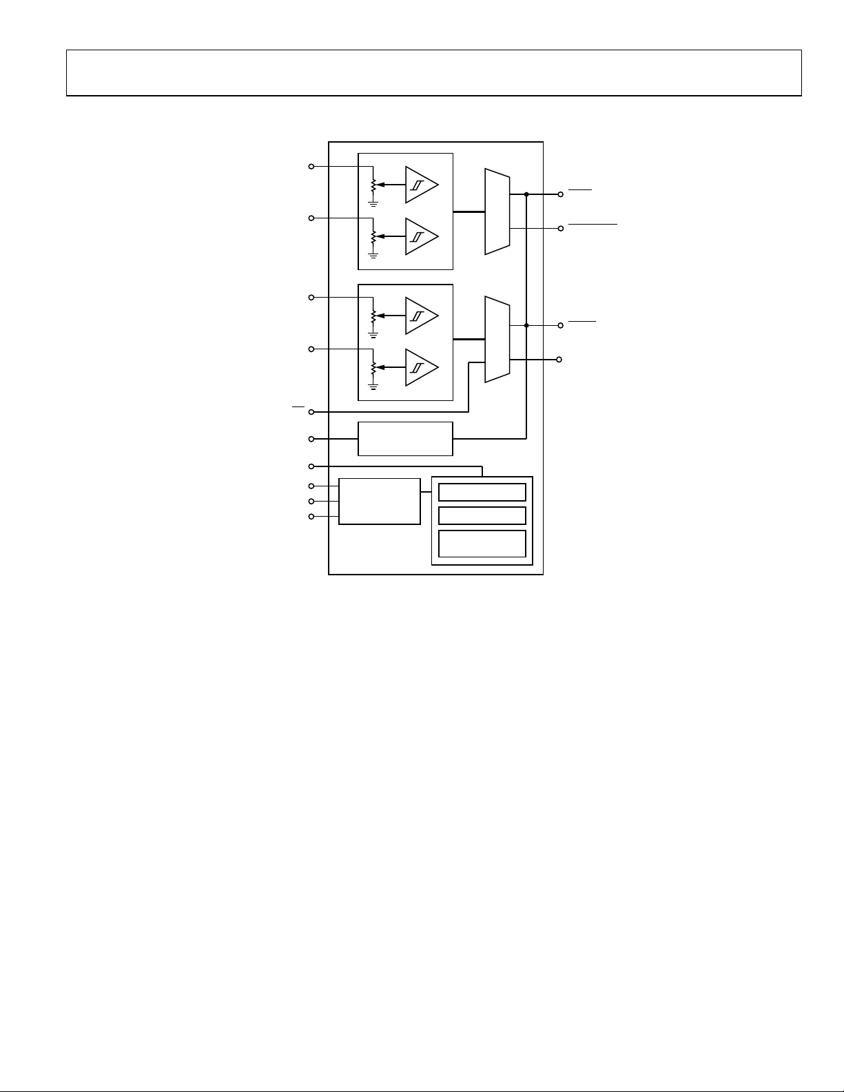
AD5100
FUNCTIONAL BLOCK DIAGRAM
V
1MON
(6V TO 30V)
V
2MON
(3V TO 30V)
V
3MON
(2.5V TO 5V)
V
4MON
(0.9V TO 30V)
MR
WDI
V
OTP
SDA
SCL
AD0
55kΩ
640kΩ
130kΩ
665kΩ
WDI DETECTION
AND
RESET GENERATOR
I2C CONTRO LLER
OV/UV
ON/OFF
OTP FUSE ARRAY
REGISTER MAP
FAULT DETECTION
Figure 1.
AD5100
SHUTDOWN
RESET
FD REGISTER
SHDN
CONTROLLER
GENERATOR
SHDNWARN
RESET
V
4OUT
05692-001
Rev. A | Page 3 of 36
Page 4

AD5100
SPECIFICATIONS
ELECTRICAL SPECIFICATIONS
6 V ≤ V
Table 2.
Parameter Symbol Conditions Min Typ1 Max Unit
HIGH VOLTAGE MONITORING INPUTS
V
1MON
V
2MON
SHDN
SHDNWARN
≤ 30 V and 3 V ≤ V
1MON
≤ 30 V, −40°C ≤ TA ≤ +125°C, unless otherwise noted.
2MON
Voltage Range V
Input Resistance R
OV, UV Threshold Tolerance
6 30 V
1MON
36 55 70 kΩ
IN_V1MON
ΔOV, ΔUV TA = 25°C −1.6 +1.6 %
(See Figure 7 and Table 6)
T
T
Hysteresis
Programmable Shutdown Hold Time
Δt
TA = 25°C; does not apply to
1SD_HOLD
Tolerance (See Figure 7 and Table 8)
Programmable Shutdown Delay Tolerance
Δt
1SD_DELAY
(See Figure 7 and Table 8)
T
= −40°C to +85°C −1.8 +1.8 %
A
= −40°C to +125°C −2 +2 %
A
1.5 %
−10 +10 %
Code 0x7
TA = 25°C; does not apply to
−10 +10 %
Code 0x7
= −40°C to +125°C; does not
A
−17 +17 %
apply to Code 0x7
Fault Detection Delay t
Glitch Immune Time t
60 μs
FD_DELAY
Guaranteed by evaluation 45 μs
GLITCH
Input Voltage V
Minimum voltage on V
2MON
ensure AD5100 V
Voltage Range2 V
Input Resistance R
On, Off Threshold Tolerance3
3 30 V
2MON
500 675 860 kΩ
IN_V2MON
ΔOn, ΔOff TA = 25°C −2 +2 %
2MON
power-up
REG
to
2.2 V
(See Figure 7 and Table 6)
T
T
= −40°C to +85°C −2.4 +2.4 %
A
= −40°C to +125°C −2.5 +2.5 %
A
Hysteresis 1.5 %
Turn-On Programmable
SHDN
Hold Time
Δt
Tolerance (See and ) Figure 7 Table 8
Turn-Off Programmable
SHDN
Delay Time
Δt
Tolerance (See and ) Figure 7 Table 8
T
TA = 25°C; does not apply to
2SD_HOLD
Code 0x7
TA = 25°C; does not apply to
2SD_DELAY
Code 0x07
= −40°C to +125°C; does not
A
−10 +10 %
−10 +10 %
−17 +17 %
apply to Code 0x7
Fault Detection Delay t
Glitch Immune Time t
SHDN
Output High
V
SHDN
Output Low
V
SHDN
Sink Current
(Open-Drain Output)
SHDNWARN
SHDNWARN
Inactive Leakage Current
Active
V
FD_DELAY
45 μs
GLITCH
only 60 μs
2MON_OFF
V
V
OH
I
V
OL
I
SINK
= V
, I
RAIL
REG
= V
RAIL
1MON
= 1.6 mA 0.4 V
SINK
= 12 V, I
1MON
V
= 12 V,
1MON
= 40 μA 2.4 V
SOURCE
, I
= 600 μA V
SOURCE
= 40 mA 1.5 3 V
SINK
SHDN
forced to 12 V
− 0.5 V
1MON
10 13.5 mA
I
OH_SHDNWARN
V
OL_SHDNWARN
0.9 μA
I
= 3 mA 0.4 V
SINK
Rev. A | Page 4 of 36
Page 5

AD5100
Parameter Symbol Conditions Min Typ1 Max Unit
LOW VOLTAGE MONITORING INPUTS
V
, V
3MON
V
Input Resistance R
V
V
V
Input Resistance R
V
V
RESET
RESET
T
V
RESET
2.7 V < V
2.3 V < V
1.8 V ≤ V
RESET
V
RESET
Glitch Immune Time t
V
V
V
WDI (WATCHDOG INPUT)
WDI Programmable Timeout Tolerance
(see Figure 13 and Table 8)
T
WDI Pulse Width t
Watchdog Initiated
Watchdog Initiated
WDI Input Voltage Low V
WDI Input Voltage High V
WDI Input Current WDI = V
WDI = 0 −20 μA
MR
(MANUAL RESET) INPUT
MR
MR
Input Current 1 μA
MR
MR
MR
4MON
Voltage Range V
3MON
Threshold Tolerance
3MON
2.0 5.5 V
3MON
85 130 180 kΩ
IN_V3MON
ΔV
T
3MON
= 25°C −2.5 +2.5 %
A
(See Figure 10 and Table 6)
Hysteresis V
3MON
Voltage Range4 V
4MON
Threshold Tolerance
4MON
3_HYSTERESIS
0.9 30 V
4MON
IN_V4MON
ΔV
T
4MON
TA = −40°C to +85°C −2.75 +2.75 %
TA = −40°C to +125°C −3 +3 %
1.2 %
500 675 860 kΩ
= 25°C −2.5 +2.5 %
A
(See Figure 12 and Table 6)
TA = −40°C to +85°C −2.75 +2.75 %
TA = −40°C to +125°C −3 +3 %
5 %
T
= 25°C; does not apply to
A
−10 +10 %
Code 0x6 and Code 0x7
= −40°C to +125°C; does not
A
−17 +17 %
Hysteresis V
4MON
Hold Time Tolerance
(See , , and ) Figure 10 Figure 12 Table 8
4_HYSTERESIS
Δt
RS_HOLD
apply to Code 0x6 and Code 0x7
60 μs
3MON/V4MON
-to-
Delay
RESET
Output Voltage High
Output Voltage Low
Output Short-Circuit Current5
Maximum Output V
4OUT
Propagation Delay t
4OUT
Maximum Frequency f
4OUT
RESET
Pulse Width
SHDN
t
RS_DELAY
V
V
OH
V
V
OL
I
SOURCE
50 μs
GLITCH
Open drain 5.5 V
4OUT_MAX
V4OUT_DELAY
V4OUT
70 μs
ΔtWD T
50 ns
WDI
When no WDI tWD/50 ms
t
WDR
When no WDI activity > 4 tWD 1 sec
t
WD_SHDN
0.3 × V
IL_WD
0.7 × V
IH_WD
≥ 4.38 V, I
3MON
3MON
= 30 μA
I
SOURCE
3MON
= 20 μA
I
SOURCE
3MON
= 8 μA
I
SOURCE
> 4.38 V, I
3MON
< 4.38 V, I
3MON
RESET
= 0, V
RESET
= 0, V
Applies to
= 25°C −10 +10 %
A
= −40°C to +125°C −17 +17 %
A
RESET
3MON
= 120 μA V
SOURCE
≤ 4.38 V,
≤ 2.7 V,
≤ 2.3 V,
= 3.2 mA 0.4 V
SINK
= 1.2 mA 0.3 V
SINK
= 5.5 V
3MON
= 3.6 V
3MON
disabled only
− 1.5 V
3MON
0.8 × V
0.8 × V
0.8 × V
V
3MON
V
3MON
V
3MON
825 μA
400 μA
10 kHz
3MON
V
3MON
160 μA
0.3 × V
Input Voltage Low
Input Voltage High
Pulse Width
Deglitching
RESET
-to-
Delay
V
IL_MR
0.7 × V
V
IH_MR
1 μs
t
MR
100 ns
t
MR_GLITCH
1 μs
t
MR_DELAY
V
3MON
3MON
V
V
Rev. A | Page 5 of 36
Page 6

AD5100
Parameter Symbol Conditions Min Typ1 Max Unit
MR
Pull-Up Resistance (Internal to V
RESET
Hold Time Tolerance
3MON
)
(see and ) Figure 12 Table 8
T
SERIAL INTERFACES
Input Logic High (SCL, SDA)6 V
Input Logic Low (SCL, SDA) VIL External R
Output Logic High (SDA) VOH V
Output Logic Low (SDA) VOL I
Input Current VIN = 0 V to 5.5 V 1 μA
Input Capacitance CI 5 pF
POWER SUPPLY
Supply Voltage Range V
Sleep Mode Supply Current I
Active Mode Supply Current I
V
Device Power-On Threshold V
V
Device Power-Up V
, Minimum Pulse Width t
2MON
Device Power-Down Delay T
I
1
Represent typical values at 25°C, V
2
Initial V
3
Does not apply if V
4
V
4MON
30 V. One application where this 30 V capability is useful is electronic media-oriented systems transport (eMOST) diagnostic circuits.
5
The
6
It is typical for the SCL and SDA to have resistors pulled up to V
turn-on minimum remains as 2.2 V but the 3 V to 30 V specifications apply afterward.
2MON
is a digital signal.
2MON
threshold limits (see Table 6) are designed to primarily allow V
RESET
short-circuit current is the maximum pull-up current when
driven directly from a low voltage logic controller without pull-up resistors.
= 12 V, and V
1MON
37 60 82 kΩ
Δt
RS_HOLD
T
= 25°C; does not apply to Code
A
−10 +10 %
0x6 and Code 0x7
= −40°C to +125°C; does not
A
−17 +17 %
apply to Code 0x06 and Code 0x7
External R
IH
6.0 30 V
1MON
SLEEP_V1MON
POWER_V1MON
2MON, IH
2MON, IL
V2MON_PW
VREG_OFF_DELAY
= 12 V.
2MON
3MON
= 2 V to 5.5 V 0.7 × V
RAIL
= 3 mA 0 0.4 V
OL
V
V
= 0 V 5 μA
2MON
= 12 V 2 mA
2MON
edge triggered mode selected 2 mA
2MON
2.2 V
0.4 V
4 ms
V
< 0.4 V (normal mode) 2 sec
2MON
2
C-initiated power-down 10 μs
to monitor low voltage inputs. The V
4MON
RESET
is driven low by a microprocessor bidirectional reset pin.
. However, care must be taken to ensure that the minimum VIH is met when the SCL and SDA are
= 2.2 kΩ 2.0 5.5 V
PULL-UP
= 2.2 kΩ 0 0.8 V
PULL-UP
V
RAIL
input pin is capable of withstanding voltages up to
4MON
Rev. A | Page 6 of 36
Page 7
AD5100
SDA
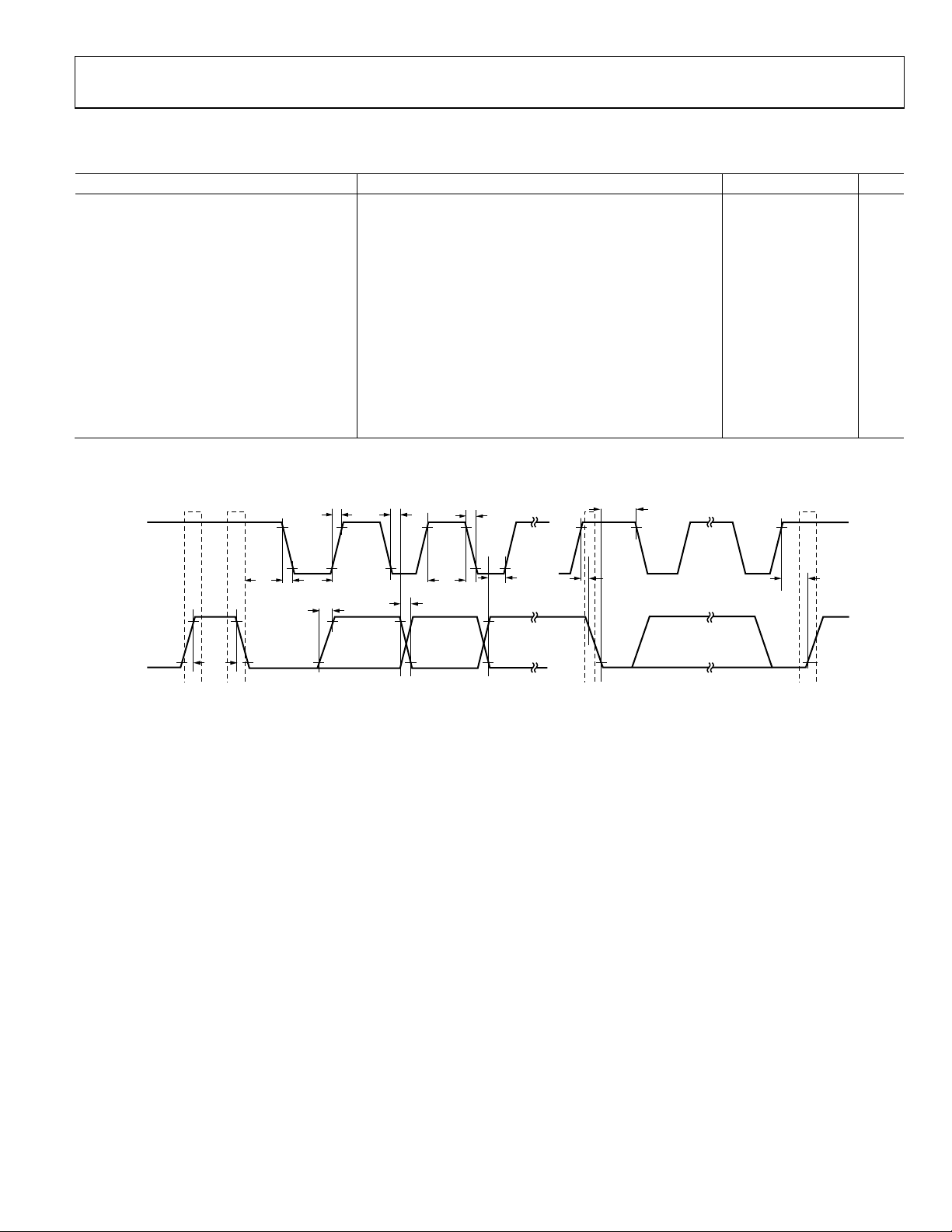
TIMING SPECIFICATIONS
Table 3.
Parameter Description Min Typ Max Unit
I2C INTERFACE TIMING CHARACTERISTICS
f
SCL clock frequency 400 kHz
SCL
t1 t
t2
t3 t
t4 t
t5 t
t6 t
t7 t
t8 t
t9 t
t10 t
1
Guaranteed by design and not subject to production test.
2
See Figure 2.
1, 2
, bus free time between start and stop 1.3 μs
BUF
, hold time after (repeated) start condition; after this
t
HD;STA
0.6 μs
period, the first clock is generated
, low period of SCL clock 1.3 μs
LOW
, high period of SCL clock 0.6 50 μs
HIGH
, setup time for start condition 0.6 μs
SU;STA
, data hold time 0.9 μs
HD;DAT
, data setup time 0.1 μs
SU;DAT
, fall time of both SDA and SCL signals 0.3 μs
F
, rise time of both SDA and SCL signals 0.3 μs
R
, setup time for stop condition 0.6 μs
SU;STO
t
t
t
8
t
9
6
2
SCL
t
t
1
PS SP
t
2
3
t
9
t
8
t
4
t
7
t
5
t
10
05692-002
Figure 2. Digital Interface Timing Diagram
Rev. A | Page 7 of 36
Page 8
AD5100
ABSOLUTE MAXIMUM RATINGS
Table 4.
Parameter Rating
V
to GND −0.3 V, +33 V
1MON
V
to GND −0.3 V, +33 V
2MON
V
to GND −0.3 V, +7 V
3MON
V
to GND −0.3 V, +33 V
4MON
V
to GND −0.3 V, +7 V
OTP
Digital Input Voltage to GND
(MR
, WDI, SCL, SDA, AD0)
Digital Output Voltage to GND
, V
(RESET
, SHDNWARN)
4OUT
Digital Output Voltage to GND (SHDN)
0 V, +7 V
0 V, +7 V
0 V, +33 V
Operating Temperature Range −40°C to +125°C
Storage Temperature Range −65°C to +150°C
ESD Rating (HBM) 3.5 kV
Maximum Junction Temperature (T
Power Dissipation1 (T
) 150°C
Jmax
Jmax
− T
2
A
)/θJA
Thermal Impedance3
θJA Junction-to-Ambient 105.44°C/W
θJC Junction-to-Case 38.8°C/W
IR Reflow Soldering (RoHS-Compliant Package)
Peak Temperature 260°C (+0°C)
Time at Peak Temperature 20 sec to 40 sec
Ramp-Up Rate 3°C/sec max
Ramp-Down Rate −6°C/sec max
Time from 25°C to Peak Temperature 8 minutes max
1
Values relate to the package being used on a 4-layer board.
2
TA = ambient temperature.
3
Junction-to-case resistance is applicable to components featuring a
preferential flow direction, for example, components mounted on a
heat sink. Junction-to-ambient resistance is more useful for air-cooled
PCB-mounted components.
Stresses above those listed under Absolute Maximum Ratings
may cause permanent damage to the device. This is a stress
rating only; functional operation of the device at these or any
other conditions above those indicated in the operational
section of this specification is not implied. Exposure to absolute
maximum rating conditions for extended periods may affect
device reliability.
ESD CAUTION
Rev. A | Page 8 of 36
Page 9
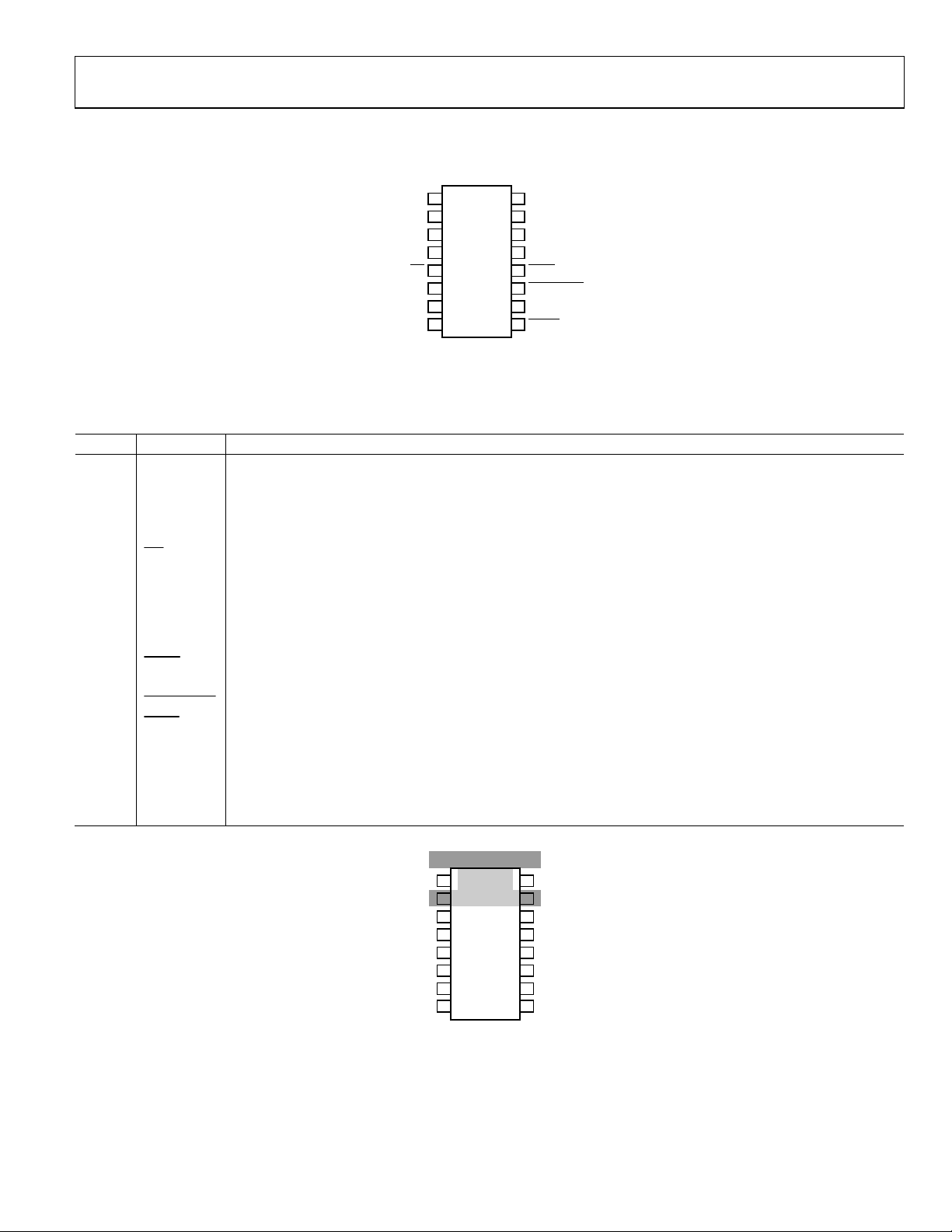
AD5100
V
V
PIN CONFIGURATION AND FUNCTION DESCRIPTIONS
1
1MON
GND
2
V
3
OTP
4
3MON
MR
5
WDI
6
7
SCL
SDA
8
NC = NO CONNECT
AD5100
TOP VIEW
(Not to S cale)
16
V
2MON
GND/NC
15
V
14
4MON
13
AD0
SHDN
12
SHDNWARN
11
10
V
4OUT
RESET
9
05692-003
Figure 3. Pin Configuration
Table 5. AD5100 Pin Function Descriptions
Pin No. Mnemonic Description
1 V
1MON
High Voltage Monitoring Input. AD5100 internal supply is derived from V
capacitor between this pin and GND, placed as close as possible to the V
. There must be a 10 μF electrolytic
1MON
pin.
1MON
2 GND Ground.
3 V
4 V
5
One-Time Programmable Supply Voltage for EPROM. A 10 μF decoupling capacitor (low ESR) to GND is required.
OTP
Low Voltage Monitoring Input.
3MON
MR
Manual Reset Input. Active low.
6 WDI Watchdog Input.
7 SCL
8 SDA
9
10 V
11
12
RESET
Open-Drain Output. Triggered by V
4OUT
SHDNWARN
Shutdown Output. Push-pull output with selectable rail voltage of V
SHDN
2
C Serial Input Register Clock. Open-drain input. If it is driven directly from a logic driver without the pull-up
I
resistor, ensure that the V
2
C Serial Data Input/Output. Open-drain input/output. If it is driven directly from a logic driver without the pull-
I
up resistor, ensure that the V
Reset. Push-pull output with rail voltage of V
Shutdown Warning. Active low, open-drain output.
minimum is 3.3 V.
IH
minimum is 3.3 V.
IH
.
4MON
3MON
.
or V
1MON
, the AD5100 internal power (30 V
REG
maximum).
13 AD0 I2C Slave Address Configuration. If tied high, this pin can only be tied to 3.3 V maximum.
14 V
Low Voltage Monitoring Input. Capable of withstanding 30 V.
4MON
15 GND/NC Ground/No Connect. Can be grounded or left floating but do not connect to any other potentials.
16 V
High Voltage Monitoring Input. It is also the internal supply voltage enabling input.
2MON
GND
1
2
3
AD5100
4
TOP VIEW
5
(Not to Scale)
6
7
8 9
Figure 4. Recommended PCB Layout for Shielded High Voltage Inputs
16
15
14
13
12
11
10
05692-004
Rev. A | Page 9 of 36
Page 10

AD5100
ONE-TIME PROGRAMMABLE (OTP) OPTIONS
All values are typical ratings; see Tab le 2 for tolerances.
Table 6. Available Programmable Thresholds at T
V
OV Threshold1 V
1MON
UV Threshold V
1MON
= 25°C
A
On Threshold V
2MON
Off Threshold2 V
2MON
Threshold V
3MON
Threshold
4MON
7.92 V 6.00 V 3.00 V 3.00 V 2.32 V 1.67 V
9.00 V 6.49 V 3.5 V 3.5 V 2.64 V 2.31 V
9.90 V 6.95 V 4.00 V 4.00 V 2.93 V3 3.05 V
11.00 V 7.47 V 4.77 V 4.77 V 3.10 V 4.62 V
12.00 V 7.92 V 6.00 V 6.00 V 4.36 V 6.51 V
13.20 V 8.43 V3 6.49 V 6.49 V 4.65 V 7.16 V
14.14 V 9.00 V 6.95 V 6.95 V3 4.75 V 7.54 V3
15.23 V 9.43 V 7.47 V3 7.47 V 4.97 V 7.96 V
15.84 V 9.90 V 7.92 V 7.92 V Reserved Reserved
17.22 V 10.42 V 8.43 V 8.43 V Reserved Reserved
18.00 V3 11.00 V 9.00 V 9.00 V Reserved Reserved
18.86 V 11.65 V 9.43 V 9.43 V Reserved Reserved
19.80 V 12.00 V 9.90 V 9.90 V Reserved Reserved
22.00 V 12.38 V 15.23 V 15.23 V Reserved Reserved
24.75 V 13.20 V 19.80 V 19.80 V Reserved Reserved
28.29 V 13.66 V 24.75 V
Rising edge triggered
Reserved Reserved
wake-up mode
1
V
must be > V
1MON_OV
2
V
is ignored if > V
2MON_OFF
3
AD5100-0 default settings. Contact Analog Devices if other default settings are required.
1MON_UV
.
2MON_ON
, but V
2MON_OFF
cannot be = V
2MON_ON
.
Table 7. Look-Up Table of Programming Code vs. Typical Thresholds Shown in Table 6
V
Code
OV
1MON
Threshold
V
UV
1MON
Threshold
V
On
2MON
Threshold
Off Threshold V
V
2MON
Threshold V
3MON
Threshold
4MON
0000 18.00 V1 8.43 V1 7.47 V1 6.95 V1 2.93 V1 7.54 V1
0001 18.86 V 7.92 V 6.95 V 7.47 V 4.65 V 1.67 V
0010 15.84 V 9.43 V 6.49 V 6.00 V 4.75 V 2.31 V
0011 17.22 V 9.00 V 6.00 V 6.49 V 4.97 V 3.05 V
0100 24.75 V 6.49 V 4.77 V 4.00 V 2.32 V 4.62 V
0101 28.29 V 6.00 V 4.00 V 4.77 V 2.64 V 6.51 V
0110 19.80 V 7.47 V 3.50 V 3.00 V 4.36 V 7.16 V
0111 22.00 V 6.95 V 3.00 V 3.50 V 3.10 V 7.96 V
1000 9.90 V 12.38 V 24.75 V 19.80 V Reserved Reserved
1001 11.00 V 12.00 V 19.80 V
Rising edge triggered
Reserved Reserved
wake-up mode
1010 7.92 V 13.66 V 15.23 V 9.90 V Reserved Reserved
1011 9.00 V 13.20 V 9.90 V 15.23 V Reserved Reserved
1100 14.14 V 10.42 V 9.43 V 9.00 V Reserved Reserved
1101 15.23 V 9.90 V 9.00 V 9.43 V Reserved Reserved
1110 12.00 V 11.65 V 8.43 V 7.92 V Reserved Reserved
1111 13.20 V 11.00 V 7.92 V 8.43 V Reserved Reserved
1
AD5100-0 default settings. Contact Analog Devices if other default settings are required.
Rev. A | Page 10 of 36
Page 11

AD5100
Table 8. Available Programmable Hold Time and Delay
t
0.07 ms 0.07 ms 0.07 ms 0.07 ms 0.1 ms 100 ms
20 ms 50 ms 10 ms1 50 ms 1 ms 250 ms
40 ms 100 ms 20 ms 100 ms1 15 ms 500 ms
60 ms 200 ms 30 ms 200 ms 30 ms 750 ms
80 ms 400 ms 40 ms 400 ms 50 ms 1000 ms
100 ms 800 ms 50 ms 800 ms 100 ms 1250 ms
150 ms 1000 ms 100 ms 1000 ms 150 ms 1500 ms1
200 ms1 1200 ms1 200 ms 1200 ms 200 ms1 2000 ms
1
Table 9. Look-Up Table of Programming Code vs. Typical Timings Shown in Table 8
Code t
000 200 ms1 1200 ms1 10 ms1 100 ms1 200 ms1 1500 ms1
001 150 ms 1000 ms 20 ms 50 ms 150 ms 2000 ms
010 100 ms 800 ms 30 ms 200 ms 100 ms 1250 ms
011 80 ms 400 ms 40 ms 400 ms 50 ms 1000 ms
100 60 ms 200 ms 50 ms 800 ms 30 ms 750 ms
101 40 ms 100 ms 100 ms 1000 ms 15 ms 500 ms
110 20 ms 50 ms 200 ms 1200 ms 1 ms 250 ms
111 0.07 ms 0.07 ms 0.07 ms 0.07 ms 0.1 ms 100 ms
1
t
1SD_HOLD
AD5100-0 default settings. Contact Analog Devices if other default settings are required.
t
1SD_HOLD
AD5100-0 default settings. Contact Analog Devices if other default settings are required.
t
1SD_DELAY
t
1SD_DELAY
t
2SD_HOLD
t
2SD_HOLD
t
2SD_DELAY
t
2SD_DELAY
t
RS_HOLD
RS_HOLD
t
WD
WD
Rev. A | Page 11 of 36
Page 12

AD5100
THEORY OF OPERATION
The AD5100 is a programmable system management IC that
has four channels of monitoring inputs. Three inputs have
high voltage (30 V) capability. For example, if the AD5100 is
used in an automotive application, V
can be connected to the battery and the V
(Monitoring Input 1)
1MON
can be connected
2MON
to the ignition switch, a rising edge trigger wake-up signal, or
the media-oriented systems transport (MOST) wake-up signal
(V
is connected to V
4MON
other inputs, V
3MON
and V
for MOST applications). Two
2MON
, are designed for low voltage
4MON
monitoring, with programmable thresholds from 2.93 V to
7.96 V. The two high voltage monitoring inputs control the
NO
V
> UV
1MON
V
< OV
1MON
V
2MON
LEVEL
SENSITIVE
SELECTED
V
> ON
2MON
V
> OFF
2MON
YES
YES
YES
YES
YES
SHDN = 0*
NO
SHDN = 0*
(V
NO
NO
NO
2MON
SENSITIVE SELE CTE D)
SHDN = 0
SHDN = 0
SHDN = 1
RISING EDGE
V
4OUT
MR = 1
YES
FLOATING
WDI DISABL ED
YES
STANDARD
WDI SELECTED
YES
VALID WDI
YES
V
>
3MON
THRESHOLD
YES
USING V
4OUT
FOR PWM
YES
V
>
4MON
THRESHOLD
YES
= 1
shutdown signal,
SHDN
and reset signal,
low voltage monitoring inputs control the reset signal,
SHDN
and
RESET
are both disabling signals for external devices.
The differences between these two outputs are in output level
and driving capabilities, as described in the section.
The WDI (watchdog) and
control the
processor. shows the general flow chart and
RESET
Figure 5 Tab le 1 0
MR
(manual reset) inputs also
output, for use with an external digital
summarizes the AD5100 functions and features.
NO
RESET = 0
NO
NO (ADVANCE WDI S E LECTED)
NO
NO
NO
NO
RESET = 0
RESET = 0
V
= 0
4OUT
V
>
4MON
THRESHOLD
YES
VALID WDI
NO
FLOATING WDI
NO
YES
RESET = 0
YES
RESET = 0
RESET = 0
SHDN = 0
RESET
Outputs
NO
, while the two
RESET
.
CONTINUE
MONITORING
DEFAULT PATHS
* SEE TABLE 11 RE S E T CONFIGURATION REG ISTER:
IF [0] = 0, THEN SHDN = 0 AND RESET = 0
IF [0] = 1, THEN SHDN = 0 AND RESET = 1
05692-005
Figure 5. General Flow Chart
Table 10. AD5100 Functions and Features
Monitoring
Input
V
V
V
Range
6 V to 28.29 V Yes Yes Yes Overvoltage/undervoltage thresholds Does not apply
1MON
3 V to 24.75 V Yes Yes Yes
2MON
2.32 V to 4.97 V No Yes Yes
3MON
Shutdown
Control
Reset
Control
Fault
Detection Functions and Features If Not Used
On/off voltage thresholds; pseudo rising edge
triggered, wake-up selectable; MOST wake-up
signal (V
connected to V
2MON
4MON
)
Connect to V
minimum input 6 V
Connect to V
set threshold to
minimum
V
1.67 V to 7.96 V No Yes Yes Additional output Connect to GND
4MON
WDI 0 V to 5 V Yes Yes No
Standard, advance, or floating; watchdog
Leave floating
selectable
MR
0 V to 5 V Yes Ye s No
Highest priority on RESET over other inputs
Leave floating
Rev. A | Page 12 of 36
1MON
OTP
,
and
Page 13

AD5100
V
MONITORING INPUTS
V
1MON
V
is a high voltage monitoring input that controls the
1MON
and
RESET
functions of the external devices. In addition,
1MON
monitors
SHDN
it provides a shutdown warning to the system. V
inputs from 6 V to 30 V.
The V
pin is monitored by two comparators, one for overvol-
1MON
tage and one for undervoltage detection. Both are designed with
1.5% hysteresis.
When the V
input goes above the programmed overvoltage
1MON
(OV) threshold, the comparator becomes active immediately,
indicating that an OV condition has occurred. Due to hysteresis,
the V
input must be brought below the programmed OV
1MON
threshold by 1.5% before the comparator becomes inactive,
indicating that the OV condition has gone away (see Figure 6).
1MON_OV
V
1MON
V
1MON_UV
When the V
OV
COMPARATOR
ACTIVE
1MON
COMPARATOR
INACTIVE
Figure 6. V
input drops below the programmed under-
HYSTERESIS
OV
COMPARATOR
ACTIVE
Hysteresis
1MON
UV
UV
COMPARATOR
INACTIVE
HYSTERESIS
voltage (UV) threshold, the comparator becomes active
immediately, indicating that a UV condition has occurred.
Similarly, due to hysteresis, the V
input must be brought
1MON
above the programmed UV threshold by 1.5% before the
comparator becomes inactive, indicating that the UV condition
has gone away.
Both V
delay timers) to control the
V
1MON
comparators are used (in conjunction with hold and
1MON
and
RESET
pins.
SHDN
has a 16-level programmable OV threshold (Register 0x01)
and UV threshold (Register 0x02) with an 8-step 0.07 ms to
200 ms shutdown hold time (t
) and 0.07 ms to 1200 ms
1SD_HOLD
shutdown delay (t
SHDN
the
signal is held low for t
within its UV and OV thresholds. The shutdown delay means
1SD_DELAY
SHDN
signal activation is delayed until the programmed
has elapsed.
that the
t
is outside the OV or UV threshold for a time longer than t
RESET
by V
IMON
follows
SHDN
.
The OV threshold chosen must be greater than the UV threshold.
When the shutdown is triggered, either because the input has
reached the OV or UV threshold, such fault conditions are
temporarily recorded in the fault detection register.
SHDNWARN
The
the shutdown output,
output is dependent on how long the shutdown-programmed
delay (t
delay (t
) is set relative to the
1SD_DELAY
). This feature attempts to allow the system to
FD_DELAY
finish any critical housekeeping tasks before shutting down the
external device.
The V
, shutdown, and shutdown warning timing diagrams
1MON
are shown in Figure 7.
The ranges of OV and UV thresholds are shown in Tabl e 6, and
5692-007
the programming codes for the selected thresholds are found in
Tabl e 7. The defaulted OV threshold is 18.00 V and, for UV
threshold, it is 8.43 V. Similarly, the ranges of shutdown hold
and delay times are shown in Tabl e 8, and the programming
codes for the selected timings are shown in Table 9 .
V
exhibits typical input resistance of 55 kΩ that users
1MON
should take into account for loading effect.
The voltage at V
1MON
a valid signal on V
power rail, V
, starts operation. Details are explained in the
REG
Power Requirements section.
). The shutdown hold time means that
1SD_DELAY
after V
1SD_HOLD
SHDN
activates once the voltage on V
1MON
returns
GLITCH
delay and hold timings when triggered
output transitions low for signaling before
SHDN
, activates. The timing of the
SHDNWARN
SHDN
propagation
provides the power for the AD5100, but
must be present before the internal
2MON
1MON
.
Rev. A | Page 13 of 36
Page 14

AD5100
V
V
1MON_OV*
V
1MON_UV*
V
2MON_ON*
V
2MON_OFF*
05692-006
)
HYSTERESIS
OFF
COMPARATOR
INACTIVE
SHDNWARN
output is dependent
) is set
2SD_DELAY
). This
FD_DELAY
SHDN
activates
V
1MON
V
2MON
t
1SD_DELAY*
t
2SD_HOLD*
SHDN
AND RESET
SHDNWARN
NOTES
1. * = PROGRAMM ABLE.
2. # = THE DURAT ION OF THE
Figure 7. V
V
2MON
V
is a high voltage monitoring input that controls the
2MON
RESET
and
functions of the external devices. V
1MON
t
FD_DELAY
and V
t
2MON
t
1SD_DELAY*
t
FD_DELAY
t
1SD_HOLD*
1SD_HOLD*
t
MUST BE SHORT E R THAN
MIN
Shutdown Timing Diagrams in Level-Sensitive Mode (Note that
SHDN
monitors
2MON
inputs from 3 V to 30 V. It has a 16-level programmable turn-on
and turn-off (on, off) hysteresis thresholds (Register 0x03 and
Register 0x04), with an 8-step 0.07 ms to 200 ms shutdown hold
time (t
(t
2SD_DELAY
The V
) and 0.07 ms to 1200 ms shutdown delay
2SD_HOLD
).
pin is monitored by two comparators, one for turn-
2MON
on and one for turn-off detection, in the level-sensitive powerup mode. Both are designed with 1.5% hysteresis. Only the
turn-on monitoring comparator is used if the rising edge
triggered wake-up mode is selected.
When the V
input goes above the programmed V
2MON
2MON
on
threshold, the comparator becomes active immediately, indicating that an on condition has occurred. Due to hysteresis, the
V
input must be brought below the programmed threshold
2MON
by 1.5% before the comparator becomes inactive, indicating that
the on condition has gone away (see Figure 8).
When the V
input drops below the programmed threshold,
2MON
the comparator becomes active immediately, indicating that a
V
off condition has occurred. Similarly, due to hysteresis,
2MON
the V
input must be brought above the programmed threshold
2MON
by 1.5% before the comparator becomes inactive, indicating that
the off condition has gone away.
t
GLITCH
t
t
GLITCH
t
#
MIN
t
t
2SD_DELAY*
VREG_OFF_DELAY
2MON_ON
V
2MON
V
2MON_OFF
By default, V
2SD_HOLD*
t
FD_DELAY
OR ELSE THE AD5100 WIL L BE POWE RE D OFF.
ON
COMPARATOR
ACTIVE
Figure 8. V
is level sensitive and the on and off thresholds
2MON
t
2SD_DELAY*
RESET
Follows
ON
COMPARATOR
INACTIVE
2MON
t
FD_DELAY
SHDN
HYSTERESIS
OFF
COMPARATOR
ACTIVE
Hysteresis
are both monitored. The on threshold chosen must be greater
than the off threshold.
When the
the V
SHDN
output is activated by the input reaching
threshold, such fault condition is temporarily
2MON_OFF
recorded in the fault detection register. The
output transitions low for signaling before the shutdown output,
SHDN
, activates. The timing of the
SHDN
on how long the shutdown programmed delay (t
relative to the
SHDNWARN
propagation delay (t
feature allows the system to finish any critical housekeeping
tasks before shutting down the external device.
once the voltage on V
than t
triggered by V
The V
RESET
.
GLITCH
2MON
, shutdown, and shutdown warning timing diagrams
2MON
is outside the threshold for a time longer
2MON
SHDN
follows
delay and hold timings when
.
are shown in Figure 7.
5692-008
Rev. A | Page 14 of 36
Page 15

AD5100
V
V
V
The ranges of on and off thresholds are shown in Ta b le 6 and
the programming codes for the selected-thresholds are found in
Tabl e 7. The default on threshold is 7.47 V and off threshold is
6.95 V. Similarly, the ranges of shutdown hold and delay times
are shown in Ta bl e 8 , and the programming codes of the selected
timings are found in Tabl e 9. The default shutdown hold time is
10 ms and the delay time is 100 ms.
V
V
If V
is ignored if V
2MON_OFF
cannot equal V
2MON_OFF
is selected with rising edge triggered wake-up mode,
2MON
is greater than V
2MON_OFF
2MON_ON.
2MON_ON
but
only the on threshold is monitored and the off threshold
is ignored. V
setting V
2MON
The voltage at V
valid signal on V
is put into rising edge triggered mode by
2MON
off threshold, Register 0x04[3:0] to 1001
provides the power for the AD5100, but a
1MON
must be present before the internal V
2MON
REG
starts operating. Details are explained in the Power Requirements
section.
V
exhibits typical input resistance of 675 kΩ that users
2MON
should take into account for loading effect.
V
3MON
V
is a low voltage monitoring input that controls the
3MON
RESET
function of an external device.
The V
pin is monitored by a comparator to detect an
3MON
undervoltage condition. It is designed with 1.5% hysteresis.
When the V
input drops below the programmed UV
3MON
threshold, the comparator becomes active immediately, indicating that a UV condition has occurred. Due to hysteresis,
the V
input must be brought above the programmed UV
3MON
threshold by 1.5% before the comparator becomes inactive,
indicating that the UV condition has gone away (see Figure 9).
t
GLITCH
3MON
UV
HYSTERESIS
05692-010
3MON_UV
UV
COMPARATOR
INACTIVE
Figure 9. V
The V
timer) to control the
V
3MON
comparator is used (in conjunction with a hold
3MON
RESET
pin.
monitors inputs from 2.0 V to 5.5 V. It has an 8-step
Hysteresis
3MON
COMPARATOR
INACTIVE
programmable reset threshold (Register 0x05) with an 8-step
0.1 ms to 200 ms reset hold time (t
means that the
above its UV threshold, until t
RESET
output remains activate when V
RS_HOLD
). The reset hold time
RS_HOLD
3MON
has elapsed. This allows
goes
the reset of an external device to be held until the programmed
time is reached.
The V
3MON
The range of thresholds is shown in and the programming
code for the selected threshold is found in . The range of
reset hold times is shown in and the programming code
of the selected timing is found in .
V
exhibits typical input resistance of 130 kΩ that users
3MON
and
RESET
timing diagrams are shown in .
Tabl e 6
Tabl e 7
Tabl e 8
Tabl e 9
Figure 10
should take into account for loading effect.
MR
The
RESET
input has an internal resistor pull-up toV
output is push-pull, between V
and GND.
3MON
3MON
. The
V
3MON
3MON
t
RS_HOLD*
t
RS_DELAY
RESET
NOTES
1. * = PROGRAMM ABLE
RESET
,
Figure 10. V
3MON
Rev. A | Page 15 of 36
Timing Diagrams
t
RS_HOLD*
t
RS_DELAY
05692-009
Page 16

AD5100
V
V
V
4MON
V
is a low voltage monitoring input that controls the
4MON
RESET
function of an external device or provides a comparator output,
V
4OUT
. The V
pin is monitored by a comparator to detect an
4MON
undervoltage condition. It is designed with 5% hysteresis.
When the V
input drops below the programmed UV thresh-
4MON
old, the comparator becomes active immediately, indicating that
a UV condition has occurred. Due to hysteresis, the V
4MON
input
must be brought above the programmed UV threshold by 5%
before the comparator becomes inactive, indicating that the UV
condition has gone away (see Figure 11).
4MON
4MON_UV
UV
COMPARATOR
INACTIVE
Hysteresis
The V
UV
COMPARATOR
INACTIVE
Figure 11. V
comparator is used to control the V
4MON
4MON
conjunction with a hold timer) to control the
configure V
to control the
4MON
to 0. Setting this bit to 1 prevents V
activate. The default setting is V
RESET
pin, set Register 0x0D[3]
from causing
4MON
does not cause
4MON
HYSTERESIS
pin and (in
4OUT
RESET
pin. To
RESET
RESET
5692-012
to
to
activate.
input voltage range is up to 30 V. It has an 8-step
V
4MON
programmable reset threshold (Register 0x06) from 1.67 V
to 7.96 V, with an 8-step 0.1 ms to 200 ms reset hold time
(t
).
RS_HOLD
The V
Figure 12 Table 6
programming code for the selected threshold is found in .
The default monitoring threshold is 7.54 V. Similarly, the range
of reset hold time is shown in , and the programming
code of the selected timing is found in .
V
4MON
should take into account for loading effect.
WATCHDOG INPUT
The watchdog input (WDI) circuit attempts to reset the system
to a known good state if a software or hardware glitch renders
the system processor inactive for a duration that is longer than
the timeout period. The timeout period, t
in eight steps from 100 ms to 2000 ms. The watchdog circuit is
independent of any CPU clock that the watchdog is monitoring.
The range of watchdog timeout is shown in Ta ble 8 , and the
programming code of the selected timeout is found in Tab l e 9 .
The default timeout is 1500 ms.
The watchdog is disabled during power-up. WDI starts monitoring once
advanced watchdog monitoring function. Register 0x0F[3] sets
the watchdog function to either standard or advanced mode.
This bit can be fixed in OTP memory.
• Register 0x0F[3] = 0: standard watchdog mode (Default)
• Register 0x0F[3] = 1: advanced watchdog mode
RESET
4MON
,
, and V
timing diagrams are shown in
4OUT
. The range of thresholds is shown in , and the
Table 8
Tabl e 8
Tabl e 9
exhibits typical input resistance of 675 kΩ that users
, is programmable
WD
RESET
is high. The AD5100 provides a standard or
t
GLITCH
V
4MON
V
4MON
t
RS_HOLD*
RESET
V
4OUT
NOTES
1. * = PROGRAMMABLE.
2. MOST AP P LICATIO NS US ING V
REQUIRE DISABLING OF V
4OUT
Figure 12. V
4MON
RESET
,
t
RS_DELAY
TRIGGE RED RESET.
4MON
, and V
4OUT
t
RS_HOLD*
Timing Diagrams
t
RS_DELAY
05692-011
Rev. A | Page 16 of 36
Page 17

AD5100
Standard Watchdog Mode
In the default standard watchdog mode, if WDI remains either
high or low for longer than the timeout period, t
WD
, a
RESET
pulse is generated in an attempt to allow the system processor
RESET
to reestablish the WDI signal. The
pulses continue
indefinitely until a valid watchdog signal, a rising or falling edge
signal at the WDI, is received. The internal watchdog timer
clears whenever a reset is asserted. The standard WDI and
RESET
timing diagrams are shown in . Figure 13
t
WDI
WDI
Advanced Watchdog Mode
The AD5100 can be programmed into an advanced watchdog
mode. In this mode, if WDI remains either high or low for longer
than the timeout period, t
WD
, a
RESET
pulse is generated, as per
standard mode. However, if the WDI input remains inactive after
three such
SHDN
is also asserted.
RESET
pulses, concurrent with the fourth
SHDN
is released after 1 second. These
RESET
pulse,
actions repeat indefinitely (unless action is taken by the user), if
the processor is not responding. The advanced WDI and
RESET
timing diagrams are shown in . Figure 14
RESET
t
WD
t
WDR
RESET PULSE CONTINUOUS PULSES UNTIL WATCHDOG AWAKES
t
= WATCHDOG-INITIATED RESET PULSE WIDTH
WDR
t
= WATCHDOG PULSE WIDTH
WDI
t
= WATCHDOG P ROGRAMMABLE TIME
WD
t
WD
t
WDR
5692-013
Figure 13. Standard Watchdog—Pulsing Reset Until Watchdog Awakes
t
WDI
WDI
t
WD
t
WDI
RESET
t
WD
t
WDR
SHDN
Figure 14. Advanced Watchdog—
3 RESET PULSES1 RESE T PULSE
t
WD_SHDN
SHUTDOWN AT 4TH RESET PUL SE RELEASE AFTER 1s
SHDN
Asserted After Three Trials of Resetting the Watchdog (
Rev. A | Page 17 of 36
SHDN
Released After 1 Second and the Cycle Repeats)
05692-014
Page 18

AD5100
Floating WDI Input
If the WDI pin is floating, the watchdog function is disabled by
default. However, floating watchdog can be enabled in the
RESET
configuration register such that a broken WDI connection or
any unusual condition that makes WDI float triggers the reset.
• Register 0x0D[3] = 0: floating WDI input does not activate
RESET
(Default)
• Register 0x0D[3] = 1: floating WDI input activates
RESET
This feature is fixed in OTP memory. Enabling or disabling the
floating WDI feature can be changed dynamically, using the
OTP overridden function is selected.
MANUAL RESET INPUT
Manual reset (MR) is an active low input to the AD5100 and
has an internal pull-up resistor to V
the
MR
pin goes low,
RESET
is activated. MR can be driven
from a CMOS logic signal.
MR
The
Note that
t
RS_HOLD
MR
has the highest priority in triggering the
RESET
and
RESET
timing diagrams are shown in .
is activated after t
after the MR signal has gone high again.
other monitoring inputs.
MR
<
t
MR_GLITCH
RESET
. If the input signal on
3MON
and is held for
MR_DELAY
RESET
t
MR
t
MR_DELAY
t
RS_HOLD*
Figure 15
over any
* = PROGRAMMABLE
Figure 15. Manual Reset (
MR
) Timing Diagram
05692-015
Rev. A | Page 18 of 36
Page 19

AD5100
V
V
OUTPUTS
SHUTDOWN OUTPUT, SHDN
The shutdown output,
over- or underthreshold values, or as the result of a failed
watchdog input.
by writing to certain registers on the AD5100.
The shutdown generator asserts a logic low
on the following conditions:
• During power-up
• When V
• When V
1MON
2MON
rising edge or the turn-off threshold during the falling
edge in level-sensitive mode (see Figure 7)
• When the external monitoring processor cannot issue
the necessary WDI signal and advanced WDI mode is
selected (see Figure 10 and Figure 9)
2
• I
C® programmed shutdown
To a c ti va t e
SHDN
enable this feature by writing to Register 0x18[4].
• Register 0x18[4] = 0: enable software control of
• Register 0x18[4] = 1: disable software control of
SHDN
, is triggered by V
SHDN
can also be asserted low at any time
1MON
SHDN
or V
2MON
signal based
goes over or under the threshold (see Figure 7)
is below the turn-on threshold during the
by writing to the part, the user must first
SHDN
SHDN
have formed across the
(V
). The dendrite is blown immediately because M2a is
1MON
designed with adequate current sinking capability and remains
in the on position to offer such protection. In another situation,
SHDN
if the
pin is hard-shorted to the 12 V battery, the shortcircuit detector opens SW2 and limits the current by the high
impedance M2b.
# *
SW1
*
SW2
NOTES
2
1. # = I
C SELECTABLE
2. * = DEFAULT
SHDN
pin and the battery terminal
1MON
#
LEVEL
M1
SHIFTER
M2A M2B
LOW-Z HIGH-Z
SHORT-CIRCUIT
DETECT
Figure 16. Shutdown Output
SW3
REG
M3
SHDN
R1
05692-016
SHDN
Once the feature is enabled, control of
is achieved by
writing to Register 0x16[2].
SHDN
• Register 0x16[2] = 0:
output not controlled by
software
SHDN
• Register 0x16[2] = 1:
SHDN
The
t
SD_HOLD
signal is released after the programmable hold time,
SHDN
. The
output is push-pull configured with an I2Cselectable rail voltage of either V
Register 0x0E[3] controls the voltage rail for
output is pulled low
in default or internal V
1MON
SHDN
REG
. This bit
can be fixed in OTP memory.
• Register 0x0E[3] = 0:
• Register 0x0E[3] =1:
Figure 16 shows the
Resistor R1 ensures that
SHDN
uses V
SHDN
uses V
SHDN
output configuration. Pull-down
SHDN
is pulled to ground when the
rail (Default)
1MON
rail
REG
AD5100 is not powered. When AD5100 is powered, M2a and
M2b are both on. M2a has relatively lower impedance than
M2b and R1 so the
SHDN
remains low at shutdown. When
the AD5100 settles, SW1 is turned on. M1 is stronger than
SHDN
M2a so
is pulled to the rail, which takes AD5100 out
of the shutdown mode.
In some applications, the AD5100 may monitor and control
power regulators where the input and enable pins are next to
each other in a fine pitch. This may pose reliability concerns
under some abnormal conditions. To prevent errors from happening, the AD5100 shutdown output features smart-load detection
to ensure that the shutdown responds. For example, if the car
battery has not started for a long time, a resistive dendrite may
Rev. A | Page 19 of 36
RESET OUTPUT, RESET
The reset output,
underthreshold values.
of the processor not generating the proper watchdog signal, if
MR
input is triggered, or if
The reset generator asserts the
following conditions:
.
• During power-up
• When V
• When V
• When
RESET
SHDN
the
• When the external monitoring processor cannot issue the
necessary WDI signal (see Figure 13 and Figure 14)
• When
RESET
is active low by default, but can be configured for active
high operation. Register 0x0D[1] controls the activation
polarity of
OTP memory.
• Register 0x0D[1] = 0:
• Register 0x0D[1] = 1:
RESET
, is triggered by V
RESET
activation can also be the result
SHDN
is activated.
RESET
drops below the threshold (see Figure 10)
3MON
drops below the threshold (see Figure 12)
4MON
SHDN
output is asserted (see and ); Figure 7 Figure 14
follows
SHDN
hold and delay timings if triggered by
3MON
signal based on the
output
MR
is asserted (see ) Figure 15
RESET
. It is possible to fix the value of this bit in
RESET
is active low (Default)
RESET
is active high
or V
4MON
Page 20

AD5100
V
RESET
The
triggered by the WDI, which is described in the
section. The
hold time, t
As shown in Figure 17, the
configured with the rail voltage of V
signal is asserted and maintained except when it is
Watch d og I np u t
RESET
signal is released after the programmable
RS_HOLD.
RESET
output is push-pull
.
3MON
3MON
M1
RESET
M2
05692-017
Figure 17. Reset Output
SHUTDOWN WARNING, SHDNWARN
An early shutdown warning is available for the system processor
to identify the source of failure and take appropriate action
before shutting down the external devices. Whenever the
voltage at V
or the voltage at V
is detected as overvoltage or undervoltage,
1MON
falls below the threshold,
2MON
SHDNWARN
outputs a Logic 0. If the processor sees a logic low on this pin,
the processor may issue an I
2
C read command to identify the
cause of failure reported in the fault detect/status register, at
Address 0x19. The processor may store the information in
external EEPROM as a record of failure history.
V
OUTPUT
4OUT
V
is an open-drain output triggered by V
4OUT
mum propagation delay, t
V4OUT_DELAY
. V
4OUT
with a mini-
4MON
can be used as a PWM
control over an external device or used as a monitoring signal.
Most applications using V
require disabling of the V
4OUT
4MON
triggered reset function. This function is disabled by writing to
Register 0x0D[2], and it is possible to fix the value of this bit in
OTP memory.
Register 0x0D[2] = 0: enables V
RESET
• Register 0x0D[2] = 1: prevents V
activating
RESET
under threshold to activate
4MON
under threshold from
4MON
Rev. A | Page 20 of 36
Page 21

AD5100
V
POWER REQUIREMENTS
INTERNAL POWER, V
The AD5100 internal power, V
becomes active when V
REG
REG
reaches 2.2 V. V
2MON
, is derived from V
is used to turn
2MON
1MON
and
AD5100 on and off with a different behavior depending on the
V
monitoring mode selection.
2MON
By default, the AD5100 turns on when the voltage at V
above the logic threshold, V
logic threshold, V
SHDN
is deasserted. Note that AD5100 requires 5 μs to start up
and that V
must be applied before V
1MON
, AD5100 turns off 2 seconds after
2MON_OFF
2MON_ON
. When V
2MON
falls below the
2MON
. Extension of the
2MON
rises
AD5100 turn-off allows the system to complete any housekeeping
tasks before the system is powered off. shows the
default V
2MON
and V
waveforms.
REG
Figure 18
Rising Edge Triggered Wake-Up Mode
If rising edge triggered wake-up V
the AD5100 does not turn off when V
mode is selected instead,
2MON
returns to a logic low.
2MON
To configure the part into rising edge triggered mode, set the
off threshold register, Register 0x04[3:1], to 1001.
V
2MON
In this mode, once the part is powered on, it can only be powered
down by an I
supply on the V
2
C power-down instruction or by removing the
pin. To power down the part over the I2C
1MON
bus while in rising edge triggered mode, the user must first
ensure that the software power down feature is enabled.
• Register 0x18[3] = 0: enable software power-down feature
• Register 0x18[3] =1: disable software power-down feature
The user must then write to Register 0x17[0], to actually power
down the AD5100.
• Register 0x17[0] = 0: AD5100 not in software power-down
• Register 0x17[0] = 1: power down AD5100
This feature is for applications that use a wake-up signal.
V
2MON_ON*
2MON
V
2MON,IH
SHDN
t
VREG_ON_DELAY
V
REG
NOTES
1. 6V < V
2. * = PROGRAMMABLE
1MON
< 30V
t
GLITCH
V
2MON_OFF*
t
2SD_HOLD*
Figure 18. Internal Power V
V
2MON_ON*
t
2SD_DELAY*
REG
V
t
2SD_HOLD*
vs. V
Timing Diagrams (Default)
2MON
2MON_OFF*
t
2SD_DELAY*
t
VREG_OFF_DELAY
t
2SD_DELAY*
t
VREG_OFF_DELAY
05692-018
Rev. A | Page 21 of 36
Page 22

AD5100
PROTECTION
For automotive applications, proper external protections on the
AD5100 are needed to ensure reliable operation. The V
likely to be used for battery monitoring. The V
is likely to
2MON
be used for ignition switch or other critical inputs. As a result,
these inputs may need additional protections such as EMI, load
dump, and ESD protections. In addition, battery input requires
reverse battery protection and short-circuit fuse protection (see
Figure 19).
Overcurrent Protection
If the V
is shorted internally in the AD5100 to GND, the
1MON
short-circuit protection kicks in and limits subsequent current
to 150 mA in normal operation.
Thermal Shutdown
When the AD5100 junction temperature is near the junction
temperature limit, it automatically shuts down and cuts out the
power from V
. The part resumes operation when the device
1MON
junction temperature returns to normal.
ESD Protection
It is common to require a contact rating of ±8 kV and a no
contact or air rating of ±15 kV ESD protection for the
automotive electronics. As a result, an ESD-rated protection
device must be used, such as MMBZ27VCL, a dual 40 W
transient voltage suppressor (TVS) at the V
1MON
and V
1MON
2MON
is
.
Load Dump Protection
A load dump is a severe overvoltage surge that occurs when the
car battery is being disconnected from a spinning alternator and
a resulting long duration, high voltage surge is introduced into
the supply line. Therefore, external load dump protection is
recommended. Typically, the load dump overvoltage lasts for a
few hundred milliseconds and peaks at around 40 V to 70 V,
while current can be as high as 1 A. As a result, a load dumprated TVS D1 and D2, such as SMCJ17, are used to handle the
surge energy. A series resistor is an inline current limiting
resistor; it should be adequate to limit the current without
significant drop and yet small enough to not affect the input
monitoring accuracy.
Reverse Battery Protection
Reverse battery protection can be provided by a regular diode
if the battery monitoring accuracy can be relaxed. Otherwise,
a 60 V P-channel power MOSFET, like the NDT2955, can be
used. Because of the MOSFET internal diode, the battery first
conducts through the P1 body diode as soon as the voltage reaches
its source terminal. The voltage divider provides adequate gateto-source voltage to turn on P1, and the voltage drop across the
FET is negligible. The resistor divider values are chosen such
that the maximum V
of the P1 is not violated and the current
GS
drawn through the battery is only a few microamps.
EMI Protection
For EMI protection, a ferrite bead or EMC rated inductor, such
as DR331-7-103, can be used.
V
B+
VMAIN
REG
V
1MON
V
2MON
DIGIPOT
EN
L1
10µH
C1
0.1µF
F1
+–
DR331-7-103
L1
C2
0.1µF
NDT2955
P1
IGNITION SWITCH
10µF
R1
2MΩ
R2
1.5MΩ
R3
2.2Ω
C3
D1
SMCJ17
R4
2.2Ω
D2
D3
SMCJ17 MMBZ27VCL
D4
DIGIPOT
VREF
AD5100
05692-020
Figure 19. Protection Circuits
Rev. A | Page 22 of 36
Page 23

AD5100
AD5100 REGISTER MAP
Tabl e 11 outlines the AD5100 register map, used to configure
and control all parameters and functions in the AD5100, and
indicates whether registers are writable, readable, or permanently
settable. All registers have the same address for read and write
operations.
The AD5100 ships from the factory with default power-up values
set in OTP memory. These default values are different for each
AD5100 model. However, nonprogrammed samples are available for evaluation purposes. The user can experiment with
different settings in the various threshold, delay, and
configuration registers.
Table 11. AD5100 Register Map
Register
Address
0x01 R/W Yes V
Read/
Write
Permanently
Settable Register Name and Bit Description
overvoltage threshold 0x00 (18.00 V)
1MON
Bit No. Description
[3:0] Four bits used to program V
[7:4] Reserved
0x02 R/W Yes V
undervoltage threshold 0x00 (8.43 V)
1MON
Bit No. Description
[3:0] Four bits used to program V
[7:4] Reserved
0x03 R/W Yes V
turn-on threshold 0x00 (7.47 V)
2MON
Bit No. Description
[3:0] Four bits used to program V
[7:4] Reserved
0x04 R/W Yes V
turn-off threshold 0x00 (6.95 V)
2MON
Bit No. Description
[3:0] Four bits used to program V
[7:4] Reserved
0x05 R/W Yes
[2:0]
RESET Threshold
V
3MON
Bit No. Description
Three bits used to program V
[7:3] Reserved
0x06 R/W Yes
[2:0]
RESET threshold
V
4MON
Bit No. Description
Three bits used to program V
[7:3] Reserved
0x07 R/W Yes
[2:0]
OV/UV triggered SHDN hold (t
V
1MON
Bit No. Description
Three bits used to program V
[7:3] Reserved
0x08 R/W Yes
[2:0]
OV/UV triggered SHDN delay (t
V
1MON
Bit No. Description
Three bits used to program V1MON OV/UV triggered SHDN
time
[7:3] Reserved
Once evaluation is complete, the user should contact Analog
Devices with their desired OTP memory default values. Analog
Devices will create an AD5100 model with the desired default
settings and factory program the AD5100 OTP memory with
these defaults.
Some users may use the AD5100 as a set-and-forget device, that
is, program some default values and never need to change these
over the life of the application. However, some users may require
on-the-fly flexibility, that is, the ability to change settings to
values other than those they choose as their defaults. Register
writing, reading, OTP, and override are explained in the I
2
C
Serial Interface section.
NonOTP Power-On
1
Default
OV threshold
1MON
UV threshold
1MON
on threshold
2MON
off threshold
2MON
0x00 (2.93 V)
RESET threshold
3MON
0x00 (7.54 V)
4MON
1SD_HOLD
)
RESET threshold
0x00 (200 ms)
OV/UV triggered SHDN hold time
1MON
)
1SD_DELAY
0x00 (1200 ms)
delay
Rev. A | Page 23 of 36
Page 24

AD5100
Register
Address
0x09 R/W Yes
[2:0]
[7:3] Reserved
0x0A R/W Yes
[2:0]
[7:3] Reserved
0x0B R/W Yes
[2:0]
[7:3] Reserved
0x0C R/W Yes Watchdog timeout (tWD) 0x00 (1500 ms)
[2:0] Three bits used to program watchdog timeout time
[7:3] Reserved
0x0D R/W Yes
[0]
[1]
[2]
[3]
[7:4] Reserved
0x0E R/W Yes
[2:0] Reserved
[3]
[7:4] Reserved
0x0F R/W Yes Watchdog mode 0x00
[2:0] Reserved
[3] 0: standard mode
1: advanced mode
[7:4] Reserved
0x15 R/W Yes Program lock (inhibit further programming) 0x00
[2:0] Reserved
[3] Reserved
[7:4] Reserved
Read/
Write
Permanently
Settable Register Name and Bit Description
turn-on triggered SHDN hold (t
V
2MON
Bit No. Description
Three bits used to program V
turn-off triggered SHDN delay (t
V
2MON
Bit No. Description
Three bits used to program V
RESET
hold (t
RS_HOLD
)
Bit No. Description
Three bits used to program RESET
Bit No. Description
configuration
RESET
Bit No. Description
0: RESET
1: RESET
0: RESET
1: RESET
0: enables V
1: prevents V
is active when SHDN is active
is not active when SHDN is active
active low
active high
under threshold, causing RESET
4MON
under threshold from causing RESET (for V
4MON
applications)
0: floating WDI does not activate RESET
1: floating WDI activates RESET
rail voltage configuration
SHDN
Bit No. Description
0: SHDN
1: SHDN
rail = V
rail = V
1MON
REG
Bit No. Description
Bit No. Description
2SD_HOLD
2MON tON
2SD_DELAY
2MON tOFF
)
triggered SHDN hold time
)
triggered SHDN delay time
hold time
4OUT
NonOTP Power-On
Default
1
0x00 (10 ms)
0x00 (100 ms)
0x00 (200 ms)
0x00
0x00
Rev. A | Page 24 of 36
Page 25

AD5100
Register
Address
0x16 R/W No Special function 1 0x00
[0] Reserved
[1] Reserved
[2]
[3] 0: override of permanent settings inactive
1: override of permanent settings active
[7:4] Reserved
0x17 R/W No Special function 2 0x00
[0] 0: software power-down of AD5100 inactive
1: software power-down of AD5100 active2
[7:1] Reserved
0x18 R/W No Disable special functions3 0x00
[0]
[1] Reserved
[2] Reserved
[3] 0: allows software power-down function
1: disables software power-down function
[4]
[7:5] Reserved
0x19
[0] 1 = V
[1] 1 = V
[2] 1 = V
[3] 1 = V
[6:4] 000: none
001: V
010: V
011: never occurred
100: V
101: V
110: V
111: never occurred
[7] Reserved
1
Default settings of AD5100-0 evaluation model only.
2
V
2MON
3
These register bits are set only. To clear them, the AD5100 must be power cycled. In some cases, the AD5100 can be connected to an I2C bus with lots of activity.
Setting these bits is an added means of ensuring that any erroneous activity on the bus does not cause AD5100 special functions to become active.
Read/
Write
Readonly
must be 0 V (that is, V
Permanently
Settable Register Name and Bit Description
Bit No. Description
0: software assertion of SHDN
1: pulls SHDN
pin low
Bit No. Description
Bit No. Description
0: allows override of any of the registers in memory except
Register 0x16 Bit[2:0] and Register 0x17 Bit[0]
1: disables override of any of the registers in memory except
Register 0x16 Bit[2:0] and Register 0x17 Bit[0]
0: allows software assertion of SHDN
1: disables software assertion of SHDN
No
Fault detect and status
(Bits[3:0] are level triggered bits that indicate the current state of the
comparators monitoring the V
1MON
and V
triggered fault detection bits that indicate what error conditions were present
when a SHDN event occurred)
Bit No. Description
input < V
2MON
input > V
2MON
input < V
1MON
input > V
1MON
UV only
1MON
OV only
1MON
below off only (default)
2MON
UV and V
1MON
OV and V
1MON
must be configured in edge sensitive mode) for software power-down.
2MON
off threshold
2MON
on threshold
2MON
UV threshold
1MON
OV threshold
1MON
below off both occurred
2MON
below off both occurred
2MON
pin is inactive
pin
pin
input pins; Bits[6:4] are edge
2MON
NonOTP Power-On
1
Default
0x40
Rev. A | Page 25 of 36
Page 26

AD5100
I2C SERIAL INTERFACE
Control of the AD5100 is via an I2C-compatible serial bus. The
AD5100 is connected to this bus as a slave device (the AD5100
has no master capabilities).
The 2-wire serial bus protocol operates as follows:
1. The master initiates data transfer by establishing a start
condition, which occurs when SDA goes from high to low
while SCL is high. The following byte is the slave address
byte, which consists of the 7-bit slave address followed by
W
an R/
bit that determines whether data is read from or
written to the slave device
2. Data is transmitted over the serial bus in sequences of nine
clock pulses (eight data bits followed by an acknowledge
bit). The transitions on the SDA line must occur during
the low period of SCL and remain stable during the high
period of SCL.
3. When all data bits have been read or written, a stop
condition is established by the master. A stop condition is
defined as a low-to-high transition on the SDA line while
SCL is high. In write mode, the master pulls the SDA line
high during the 10
th
clock pulse to establish a stop condition. In the read mode, the master issues a no acknowledge
for the ninth clock pulse (that is, the SDA line remains
high). The master then brings the SDA line low before the
th
10
clock pulse and high during the 10th clock pulse to
establish a stop condition.
For the AD5100, write operations contain either one or two
bytes, while read operations contain one byte. The AD5100
makes use of an address pointer register. This address pointer
sets up one of the other registers for the second byte of the write
operation or for a subsequent read operation. Tabl e 12 shows
the structure of the address pointer register. Bits [6:0] signify
the address of the register that is to be written to or read from.
Bit 7 is a reserved bit and should be 0 for normal write/read
operations.
Table 12. Address Pointer Register Structure
Bit Number Function
7 Reserved
6 Address Bit 6
5 Address Bit 5
4 Address Bit 4
3 Address Bit 3
2 Address Bit 2
1 Address Bit 1
0 Address Bit 0 (LSB)
SCL
The serial input register clock pin shifts in one bit at a time
on positive clock edges. An external 2.2 kΩ to 10 kΩ pull-up
resistor is needed. The pull-up resistor should be tied to V
provided V
is sub-5 V.
3MON
3MON
,
SDA
The serial data input/output pin shifts in one bit at a time on
positive clock edges, with the MSB loaded first. An external
2.2 kΩ to 10 kΩ pull-up resistor is needed. The pull-up resistor
should be tied to V
, provided V
3MON
is sub-5 V.
3MON
AD0
The AD5100 has a 7-bit slave address. The six MSBs are 010111,
and the LSB is determined by the state of the AD0 pin. When the
2
C slave address pin, AD0, is low, the 7-bit AD5100 slave address
I
is 0101110. When AD0 is high, the 7-bit AD5100 slave address
is 0101111 (pulled up to 3.3 V maximum).
The AD0 pin allows the user to connect two AD5100 devices
to the same I
2
C bus . Tabl e 13 and Figure 20 show an example
of two AD5100 devices operating on the same serial bus
independently.
Table 13. Slave Address Decoding Scheme
AD0 Programming Bit AD0 Device Pin Device Addressed
0 0 V 0x2E (U1)
1 3.3 V max 0x2F (U2)
5V
3.3V MAX
Rp
SDA
SCL
5V
SDA
SCL
AD0
AD5100
U2
05692-021
Rp
MASTER
SDA
SCL
AD0
AD5100
U1
Figure 20. Two AD5100 Devices on One Bus
Rev. A | Page 26 of 36
Page 27

AD5100
WRITING DATA TO AD5100
When writing data to the AD5100, the user begins by writing
W
an address byte followed by the R/
bit set to 0. The AD5100
acknowledges (if the correct address byte is used) by pulling
the SDA line low during the ninth clock pulse. The user then
follows with two data bytes. The first data byte is the address of
the internal data register to be written to, which is stored in the
address pointer register. The second byte is the data to be written
to the internal data register. After each byte, the AD5100
acknowledges by pulling the SDA line low during the ninth
clock pulse. illustrates this operation. Figure 21
READING DATA FROM AD5100
When reading data from an AD5100 register, there are two
possibilities.
• If the AD5100 address pointer register value is unknown
or not at the desired value, it is first necessary to set it to
the correct value before data can be read from the desired
data register. This is done by performing a write to the
AD5100, but only a value containing the register address
is sent because data is not to be written to the register. This
is shown in Figure 22. A read operation is then performed
consisting of the serial bus address, R/
followed by the data byte from the data register. This is
shown in . Figure 23
SCL
SDA
START BY
MASTER
01011
FRAME 1
SLAVE ADDRESS BYTE
Figure 21. Writing a Register Address to the Address Pointer Register, Then Writing Data to the Selected Register
SCL
SDA
START BY
MASTER
SCL
SDA
START BY
MASTER
W
bit set to 1,
1
R/W
ACK. BY
AD5100
FRAME 1
OTP
AD0
01011
SLAVE ADDRESS BYTE
Figure 22. Dummy Write to Set Proper Address Pointer
01011
FRAME 1
SLAVE ADDRESS BYTE
Figure 23. Read Data from the Address Pointer Register
AP5 AP4
AP6
ADDRESS POINT E R BY T E
1
AD0
1
AD0
R/W
ACK. BY
AD5100
R/W
ACK. BY
AD5100
• If the address pointer is known to be already at the desired
address, data can be read from the corresponding data
register without first writing to the address pointer register.
Tabl e 14 shows the readback data byte structure. Bits[6:0] contain the data from the register just read. Bit 7 is a reserved bit
and should be ignored for normal read operations. The majority
of AD5100 registers are four bits wide, with only the fault detect
and status register and disable special functions register at seven
bits and five bits wide, respectively.
Table 14. Readback Data Byte Structure
Bit Number Function
7 Reserved
6 D6
5 D5
4 D4
3 D3
2 D2
1 D1
0 D0 (LSB)
AP3
FRAME 2
AP1
AP2
OTP
AP5
AP6
ADDRESS POINTER BYTE
OTP
OK
D5
D6
AP0
D7
ACK. BY
AD5100
AP3
AP4
AP2
FRAME 2
D3
D4
D2
FRAME 2
READ DATA BYTE
D6 D5 D4 D3 D2 D1
FRAME 3
DATA BYTE
AP1
AP0
ACK. BY
AD5100
STOP BY
MASTER
D0
D1
NO ACK. B Y
MASTER
STOP BY
MASTER
D0
ACK. BY
AD5100
5692-023
5692-024
STOP BY
MASTER
5692-022
Rev. A | Page 27 of 36
Page 28

AD5100
TEMPORARY OVERRIDE OF DEFAULT SETTINGS
Even with OTP-Programmed parts, it is possible to temporarily
override the default values of any of the permanently programmable registers. To override a permanent setting in a particular
register (when the lock bit is programmed), the following sequence
should be used:
1. Set Bit 3 = 1 in Register 0x16 (special function 1).
2. Write the desired temporary data to the register of choice.
While the override bit (Bit 3) is set in Register 0x16, the user
can override any registers by simply writing to them with new data.
To reset an overridden register to its default setting, the
following sequence should be used:
1. Set Bit 3 = 0 in Register 0x16.
2. Write a dummy byte to the register of choice.
Clearing the override bit in Register 0x16 does not cause all
overridden registers to revert to their defaults at the same time.
For example, imagine that the user overrides Register 0x01,
Register 0x02, and Register 0x03.
If the user subsequently clears the override bit in Register 0x16
and writes a dummy byte to Register 0x01, Register 0x01 reverts
to its default value. However, Register 0x02 and Register 0x03
still contain their override data. To revert both registers to their
default values, the user must write dummy data to each register
individually.
Power cycling the AD5100 also resets all registers to their
programmed defaults.
Rev. A | Page 28 of 36
Page 29

AD5100
APPLICATIONS INFORMATION
CAR BATTERY AND INFOTAINMENT SYSTEM SUPPLY MONITORING
The AD5100 has two high voltage monitoring inputs with shutdown and reset controls over external devices. For example, the
V1MON and V2MON can be used to monitor the signals from
a car battery and an ignition key in an automobile, respectively
(see Figure 24). The shutdown output can be connected to the
shutdown pin of an external regulator to prevent false conditions such as a weak battery or overcharging of a battery by an
alternator. The reset output can be used to reset the processor in
the event of a hardware or software malfunction. An example of
the input and output responses of this circuit is shown in Figure 25.
Rev. A | Page 29 of 36
Page 30

AD5100
+5V
VOUT
V
VIN
+3.3
GND
REG1
SD
REG2
V
VIN VOUT
SD GND
PA
VCC
05692-025
AD5100
V
REG
SHDN
LOAD
DESELECT
DRIVER
PROGRAMMABLE
AND
AND
SHDN
HOLD
SHUTDOWN
CONTROLLER
FD
OSC
VREF
EN
REG
V
NDT2955
OV
1MON
V
D1
R3
2.2Ω
C3
10µF
P1
L1
10µH
DR331-7-103
C1
0.1µF
UV
DIGIPOT
SMCJ17
R1
R2
2MΩ
1.5MΩ
L1
F1
DELAY
ADJUSTABLE
FD
2MON
V
R4
2.2Ω
IGNITION SWITCH
B+
FD
C
2
SHDN
1
ON
DIGIPOT
D4
D3
D2
C2
0.1µF
+–
VMAIN
DAC
OFF
3MON
V
SMCJ17 MMBZ27VCL
RESET
132
RESET
DIGIPOT
4OUT
V
DRIVER
AND
HOLD
RESET
GENERATOR
ADJUSTABLE
DIGIPOT
4MON
V
4 TIMES
RESET
3MON
V
MR
GENERATOR
WATCHDOG
PROGRAMMABLE
3MON
V
C3
0.1µF
WDI
C2
10µF
VOTP
I/O
I/O
DSP/
VDD
DVDD
MICROPROCESSOR
1.8V
RESET
3.3V
SHDNWARN
SET CONFIGURATIONS
PROGRAM PARAMETERS
READ STATUS
FD REGISTER
MEMORY MAP
OTP FUSE ARRAY
(FAULT DETECTION)
C
2
I
SHDN
C
2
I
CONTROLLER
R3
R2
SCL
AD0
SDA
DAC
CODEC
IN OUT
SIGNAL
Figure 24. Typical DSP in Car Infotainment Application
Rev. A | Page 30 of 36
Page 31

AD5100
BATTERY
IGNITION
SHDN
RESET
V
3.3V
REG
WDI
MR
OV
UV
<
t
GLITCH
t
VREG_ON_DELAY
UV
SHUTDOWN
5V
HIGH-Z
SHUTDOWN
ENABLE
RESET
Figure 25. Example of
+5V
BROWNOUT
RESET
SHDN
and
WDI
RESET
RESET
Responses of Circuit Shown in Figure 24
MR
RESET
WDI RESET
t
VREG_OFF_DELAY
MICROPROCESSOR
FAILED
SHUTDOWN
MICROPROCESSOR
FAILED
RESET
HIGH-Z
V
2MON
OFF
SHUTDOWN
SHUTDOWN
ENABLE
RESET
05692-026
Rev. A | Page 31 of 36
Page 32

AD5100
V
V
BATTERY MONITORING WITH FAN CONTROL
V
can be used with V
4MON
control circuit. For example, as shown in Figure 26, when a
temperature sensor output connects to the V
the proper threshold level set, V
temperature goes above the threshold. This turns on the FET
switch, which activates the fan. When V
threshold, V
decreases, which turns off the fan.
4OUT
in tandem to form a simple PWM
4OUT
input, with
4MON
outputs high whenever the
4OUT
drops below the
TEMP
BATTERY STATE OF CHARGE INDICATOR AND SHUTDOWN EARLY WARNING MONITORING
In the automotive application, the system designer may set the
battery threshold to the lowest level to allow an automobile to
start at the worst-case condition. If the battery remains at the
low voltage level, it is indeed a poor battery. However, there is
no way to warn the driver. As a result, the system designer can
use V
the battery voltage monitored at V
gives a battery replacement warning. The circuit is shown in
Figure 28.
as the battery warning indicator. By stepping down
4OUT
, the LED is lit, which
4MON
VTEMP
TMP35
V
REG
PA
MR
WDI
05692-027
CLK
BATTERY
IGNITION
V
REG
V
TEMP
MR
WDI
V
1MON
V
2MON
V
3MON
V
4MON
MR
WDI
SCL
SDA
AD5100
SHDNWARN
BATTERY
SHDN
V
4OUT
RESET
V
REG
SD
MICROPROCESSOR
CLK MISO/MOSI
Figure 26. Power Amp Monitoring and Fan Control
TEMP
V
4OUT
NOTES
1. V
4MON
RESET DISABL E D.
Figure 27. V
with Respect to V
4OUT
TEMP
, with V
4MON
RESET
Disabled in Circuit Shown in Figure 26
THRESHOLD
4MON
05692-028
BATTERY
IGNITION
V
V
2MON
1MON
SHDN
AD5100
CLK
V
4MON
SCL
SDA
V
4OUT
SHDNWARN
MICROPROCESSOR
CLK MISO/MOSI
05692-029
Figure 28. Battery State of Charge Indication
Rev. A | Page 32 of 36
Page 33

AD5100
RISING EDGE TRIGGERED WAKE-UP MODE
As indicated in Figure 29, the microprocessor can control its
own power-down sequence using the rising edge triggered
wake-up signal. The operator must select the rising edge
triggered wake-up mode setting for the V
threshold value, as shown in Tabl e 6, by setting Register
0x04[3:1] = 1001.
When the rising edge wake-up signal is detected by V
the AD5100 is powered up with the
SHDN
The external regulator is turned on to supply power to the
microprocessor. A reset pulse train is generated at the reset
turn-off
2MON
2MON
pin pulled high.
,
output if there is no watchdog activity. The pulse continues
until the correct watchdog signal appears at the AD5100 WDI
pin. The shutdown pin remains high as long as the AD5100
continues to receive the correct watchdog signal.
When the microprocessor finishes its housekeeping tasks or
powers down the software routine, it stops sending a watchdog
signal. In response, the AD5100 generates a reset. The shutdown pin is pulled low 2 seconds after, and the regulator output
drops to 0 V, which shuts down the microprocessor. At that
point, the AD5100 enters sleep mode.
Rev. A | Page 33 of 36
Page 34

AD5100
V
2
V
VIV
O
V
REG
SHDN
SD
CAN WAKE
UP PULSE(S)
BATTERY
V
V
1MON
2MON
AD5100
V
DD
MICROPROCESSOR
RS
I/O
I/O
I/O
SCL
SDA
WDI
RESET
05692-030
Figure 29. Rising Edge Triggered Wake-Up Mode
V
2MON
WDI
RESET
SCL
SCL
SDA
SHDN
NOTES
1. 6V <
. SELECT
1MON
< 30V.
= RISING EDGE TRIG GER/CAN WAKE UP MODE.
2MON_OFF
SDA WRITE
05692-031
Figure 30. Rising Edge Triggered Operation of Circuit Shown in Figure 29
Rev. A | Page 34 of 36
Page 35

AD5100
OUTLINE DIMENSIONS
0.197 (5.00)
0.193 (4.90)
0.189 (4.80)
0.065 (1.65)
0.049 (1.25)
0.010 (0.25)
0.004 (0.10)
COPLANARITY
0.004 (0.10)
16
1
0.025 (0.64)
BSC
CONTROLL ING DIMENSIONS ARE IN INCHES; MILLIMETERS DIMENSI ONS
(IN PARENTHESES) ARE ROUNDED-OFF INCH EQUIVALENTS FOR
REFERENCE ONLYAND ARE NOT APP ROPRIATE FOR USE I N DE S IGN.
9
0.158 (4.01)
0.154 (3.91)
0.150 (3.81)
8
0.069 (1.75)
0.053 (1.35)
SEATING
0.012 (0.30)
0.008 (0.20)
COMPLI ANT TO JEDEC STANDARDS MO-137-AB
PLANE
0.244 (6.20)
0.236 (5.99)
0.228 (5.79)
8°
0°
0.010 (0.25)
0.006 (0.15)
0.050 (1.27)
0.016 (0.41)
0.020 (0.51)
0.010 (0.25)
0.041 (1.04)
REF
012808-A
Figure 31. 16-Lead Shrink Small Outline Package [QSOP]
(RQ-16)
Dimensions shown in inches
ORDERING GUIDE
1, 2
Model
Temperature Range Package Description Package Option Ordering Quantity
AD5100YRQZ-0 −40°C to +125°C 16-Lead QSOP RQ-16
AD5100YRQZ-1RL7 −40°C to +125°C 16-Lead QSOP RQ-16 1,000
AD5100YRQZ-1REEL −40°C to +125°C 16-Lead QSOP RQ-16 2,500
EVAL-AD5100EBZ Evaluation Board
1
Z = RoHS Compliant Part.
2
AD5100YRQZ-0 = Non-OTP programmed part, intended for evaluation purposes only.
AUTOMOTIVE PRODUCTS
The AD5100 models are available with controlled manufacturing to support the quality and reliability requirements of automotive
applications. Note that these automotive models may have specifications that differ from the commercial models; therefore, designers
should review the Specifications section of this data sheet carefully. Only the automotive grade products shown are available for use in
automotive applications. Contact your local Analog Devices account representative for specific product ordering information and to
obtain the specific Automotive Reliability reports for these models.
Rev. A | Page 35 of 36
Page 36

AD5100
NOTES
I2C refers to a communications protocol originally developed by Philips Semiconductors (now NXP Semiconductors).
©2009–2010 Analog Devices, Inc. All rights reserved. Trademarks and
registered trademarks are the property of their respective owners.
D05692-0-6/10(A)
Rev. A | Page 36 of 36
 Loading...