

VOICEBAND
ANALOG
INPUT A
VOICEBAND
ANALOG
INPUT B
DIFFERENTIAL
ANALOG
OUTPUT
DIGITAL
DATA AND
CONTROL
SERIAL
PORT
16-BIT
SIGMA-
DELTA DAC
16-BIT
SIGMA-
DELTA ADC
MUX
+20dB
AMP
VOLTAGE
REFERENCE
PGA
a
Voiceband Signal Port
AD28msp02
FEATURES
Complete Analog I/O Port for Voiceband DSP
Applications
Linear-Coded 16-Bit Sigma-Delta ADC
Linear-Coded 16-Bit Sigma-Delta DAC
On-Chip Anti-Aliasing and Anti-lmaging Filters
On-Chip Voltage Reference
8 kHz Sampling Frequency
Twos Complement Coding
65 dB SNR + THD
Programmable Gain on DAC and ADC
Serial Interface To DSP Processors
24-Pin DlP/28-Lead SOIC
Single 5 V Power Supply
GENERAL DESCRIPTION
The AD28msp02 Voiceband Signal Port is a complete analog
front end for high performance voiceband DSP applications.
Compared to traditional µ-law and A-law codecs, the
AD28msp02’s linear-coded ADC and DAC maintain wide
dynamic range while maintaining superior SNR and THD. A
sampling rate of 8.0 kHz coupled with 65 dB SNR + THD performance make the AD28msp02 attractive in many telecom and
speech processing applications, for example digital cellular radio
and high quality telephones. The AD28msp02 simplifies overall
system design by requiring only a single +5 V power supply.
The inclusion of on-chip anti-aliasing and anti-imaging filters,
16-bit sigma-delta ADC and DAC, and programmable gain
amplifiers ensures a highly integrated and compact solution to
voiceband analog processing requirements. Sigma-delta conversion technology eliminates the need for complex off-chip antialiasing filters and sample-and-hold circuitry.
The AD28msp02’s serial I/O port provides an easy interface to
host DSP microprocessors such as the ADSP-2101, ADSP-2105
and ADSP-2111. The AD28msp02 is available in a 24-pin, 0.3"
plastic DIP and a 28-lead SOIC package.
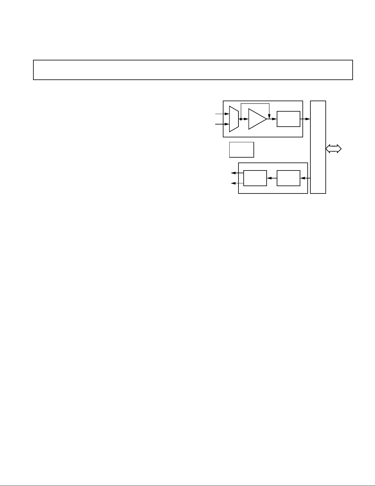
FUNCTIONAL DESCRIPTION
Figure 1 shows a block diagram of the AD28msp02.
A/D CONVERSION
The A/D conversion circuitry of the AD28msp02 consists of two
analog input amplifiers, an optional 20 dB preamplifier, and
a sigma-delta analog-to-digital converter (ADC). The analog
input signal to the AD28msp02 must be ac-coupled.
REV. 0
Information furnished by Analog Devices is believed to be accurate and
reliable. However, no responsibility is assumed by Analog Devices for its
use, nor for any infringements of patents or other rights of third parties
which may result from its use. No license is granted by implication or
otherwise under any patent or patent rights of Analog Devices.
FUNCTIONAL BLOCK DIAGRAM
Analog Input Amplifiers
The two analog input amplifiers (NORM, AUX) are internally
biased by an on-chip voltage reference in order to allow operation of the AD28msp02 with a single +5 V power supply.
An analog multiplexer selects either the NORM or AUX amplifier as the input to the ADC’s sigma-delta modulator. The
optional 20 dB preamplifier may be used to increase the signal
level; the preamplifier can be inserted before the modulator or
can be bypassed. Input signal level to the sigma-delta modulator
should not exceed V
, which is specified under “Analog
INMAX
Interface Electrical Characteristics.” Refer to “Analog Input” in
the “Design Considerations” section of this data sheet for more
information.
The input multiplexer and 20 dB preamplifier are configured by
Bits 0 and 1 (IPS, IMS) of the AD28msp02’s control register. If
the multiplexer setting is changed while an input signal is being
processed, the ADC’s output must be allowed time to settle to
ensure that the output data is valid.
ADC
The ADC consists of a 2nd-order analog sigma-delta modulator,
an anti-aliasing decimation filter, and a digital high-pass filter.
The sigma-delta modulator noise-shapes the signal and produces 1-bit samples at a 1.0 MHz rate. This bit stream, which
represents the analog input signal, is fed to the anti-aliasing
decimation filter.
Decimation Filter
The anti-aliasing decimation filter contains two stages. The first
stage is a sinc
4
digital filter that increases resolution to 16 bits
and reduces the sample rate to 40 kHz. The second stage is an
IIR low-pass filter.
One Technology Way, P.O. Box 9106, Norwood, MA 02062-9106, U.S.A.
Tel: 617/329-4700 Fax: 617/326-8703
AD28msp02
VFB
NORM
VIN
NORM
VFB
AUX
VIN
AUX
V
REF
VOUT
P
VOUT
N
VOLTAGE
REFERENCE
OUTPUT
DIFFERENTIAL
AMP
NORM
AUX
INPUT
AMP
INPUT
AMP
PGA
MUX
16-BIT SIGMA-DELTA ADC
+20dB
AMP
ANALOG
SMOOTHING
FILTER
1.0
MHz
1
SIGMA-DELTA
MODULATOR
SIGMA-DELTA
MODULATOR
ANALOG
16-BIT SIGMA-DELTA DAC
DIGITAL
1.0
MHz
1.0
MHz
1
16
ANTI-ALIASING
DECIMATION
FILTER
ANTI-IMAGING
INTERPOLATION
FILTER
Figure 1. AD28msp02 Block Diagram
8.0
kHz
16
DIGITAL
HIGH-PASS
FILTER
CONTROL
REGISTER
DIGITAL
HIGH-PASS
FILTER
16 16
8.0
kHz
kHz
8.0
kHz
SDOFS
SDO
8.0
DATA/
SERIAL
PORT
16
CNTRL
SCLK
SDI
SDIFS
CS
The IIR low-pass filter is a 10th-order elliptic filter with a passband edge at 3.7 kHz and a stopband attenuation of 65 dB at
4 kHz. This filter has the following specifications:
Filter type: 10th-order low-pass elliptic IIR
Sample frequency: 40.0 kHz
Passband cutoff:* 3.70 kHz
Passband ripple: ±0.2 dB
Stopband cutoff: 4.0 kHz
Stopband ripple: –65.00 dB
*The passband cutoff frequency is defined to be the last point in the passband
that meets the passband ripple specification.
(Note that these specifications apply only to this filter, and not to the entire
ADC. The specifications can be used to perform further analysis of the exact
characteristics of the filter, for example using a digital filter design software
package.)
Figure 2 shows the frequency response of the IIR low-pass filter.
0
–20
–40
–60
LOG MAGNITUDE – dB
–80
–100
2000
FREQUENCY – Hz
4400380032002600
5000
Figure 2. IIR Low-Pass Filter Frequency Response
High-Pass Filter
The digital high-pass filter removes frequency components at
the low end of the spectrum; it attenuates signal energy below
the passband of the converter. The high-pass filter can be
bypassed by setting the ADBY bit (Bit 3) of the AD28msp02’s
control register.
The high-pass filter is a 4th-order elliptic filter with a passband
cutoff at 150 Hz. Stopband attenuation is 25 dB. This filter has
the following specifications:
Filter type: 4th-order high-pass elliptic IIR
Sample frequency: 8.0 kHz
Passband cutoff: 150.0 Hz
Passband ripple: ±0.2 dB
Stopband cutoff: 100.0 Hz
Stopband ripple: –25.00 dB
(Note that these specifications apply only to this filter, and not to the entire
ADC. The specifications can be used to perform further analysis of the exact
characteristics of the filter, for example using a digital filter design software
package.)
Figure 3 shows the frequency response of the high-pass filter.
0
–20
–40
–60
LOG MAGNITUDE – dB
–80
–100
0
FREQUENCY – Hz
24018012060
300
Figure 3. High-Pass Filter Frequency Response
Passband ripple is ±0.2 dB for the combined effects of the
ADC’s digital filters (i.e., high-pass filter and IIR low-pass of
the decimation filter) in the 300 Hz–3400 Hz passband.
The output of the ADC is transferred to the AD28msp02’s
serial port (SPORT) at an 8 kHz rate, for transmission to the
host DSP processor. Maximum group delay in the ADC will not
exceed 1 ms in the region from 300 Hz to 3 kHz.
–2–
REV. 0

AD28msp02
PIN DESCRIPTIONS
Pin Name I/O/Z Function
VIN
NORM
I Analog input to inverting terminal of
NORM input amplifier.
VFB
VIN
NORM
AUX
O Output terminal of NORM amplifier.
I Analog input to inverting terminal of
AUX input amplifier.
VFB
AUX
VOUT
P
O Output terminal of AUX amplifier.
O Analog output from noninverting
terminal of differential output amplifier.
VOUT
N
O Analog output from inverting terminal of
differential output amplifier.
V
REF
O On-chip bandgap voltage reference
(2.5 V ± 10%).
MCLK I Master clock input; frequency must
equal 13.0 MHz to guarantee listed
specifications.
SCLK O/Z Serial clock used to clock data or control
bits to and from the serial port
(SPORT). The frequency of SCLK is
equal to the frequency of the master
clock (MCLK) divided by 5. SCLK is
3-stated when CS is low.
SDI I Serial data input of SPORT. Both data
and control information are input on
this pin. Input at SDI is ignored when
CS is low.
SDO O/Z Serial data output of SPORT. Both data
and control information are output on
this pin. SDO is 3-stated when CS is
low.
SDIFS I Framing signal for SDI serial transfers.
Input at SDIFS is ignored when CS is
low.
SDOFS O/Z Framing signal for SDO serial transfers.
SDOFS is 3-stated when CS is low.
DATA/
CNTRL I Configures AD28msp02 for either data
or control information transfers (via
SPORT).
CS I Active-high chip select. Can be used to
3-state the SPORT interface; when CS
is low, the SCLK, SDO, and SDOFS
outputs are 3-stated and the SDI and
SDIFS inputs are ignored. If CS is de-
asserted during a serial data transfer, the
16-bit word being transmitted is lost.
RESET I Active low reset signal; resets Control
Register and clears digital filters.
RESET
does not 3-state the SPORT outputs
(SCLK, SDO, SDOFS).
V
CC
GND
V
DD
GND
A
D
Analog supply voltage; nominal +5 V.
Analog ground.
Digital supply voltage; nominal +5 V.
Digital ground.
D/A CONVERSION
The D/A conversion circuitry of the AD28msp02 consists of a
sigma-delta digital-to-analog converter (DAC), an analog
smoothing filter, a programmable gain amplifier, and a differential output amplifier.
DAC
The AD28msp02’s sigma-delta DAC implements digital filters
and a sigma-delta modulator with the same characteristics as the
filters and modulator of the ADC. The DAC consists of a digital
high-pass filter, an anti-imaging interpolation filter, and a digital
sigma-delta modulator.
The DAC receives 16-bit samples from the host DSP processor
via AD28msp02’s serial port at an 8 kHz rate. If the host processor fails to write a new value to the serial port, the existing
(previous) data is read again. The data stream is filtered first by
the DAC’s high-pass filter and then by the anti-imaging interpolation filter. These filters have the same characteristics as the
ADC’s anti-aliasing decimation filter and digital high-pass filter.
The output of the interpolation filter is fed to the DAC’s digital
sigma-delta modulator, which converts the 16-bit data to 1-bit
samples at a 1.0 MHz rate. The modulator noise-shapes the signal such that errors inherent to the process are minimized in the
passband of the converter. The bit stream output of the sigmadelta modulator is fed to the AD28msp02’s analog smoothing
filter where it is converted to an analog voltage.
High-Pass Filter
The digital high-pass filter of the AD28msp02’s DAC has the
same characteristics as the high-pass filter of the ADC. The
high-pass filter removes frequency components at the low end of
the spectrum; it attenuates signal energy below the passband of
the converter. The DAC’s high-pass filter can be bypassed by
setting the DABY bit (Bit 2) of the AD28msp02’s control
register.
The high-pass filter is a 4th-order elliptic filter with a passband
cutoff at 150 Hz. Stopband attenuation is 25 dB. This filter has
the following specifications:
Filter type: 4th-order high-pass elliptic IIR
Sample frequency: 8.0 kHz
Passband cutoff: 150.0 Hz
Passband ripple: ±0.2 dB
Stopband cutoff: 100.0 Hz
Stopband ripple: –25.00 dB
(Note that these specifications apply only to this filter, and not to the entire DAC.
The specifications can be used to perform further analysis of the exact characteristics of the filter, for example using a digital filter design software package.)
Figure 3 shows the frequency response of the high-pass filter.
Interpolation Filter
The anti-imaging interpolation filter contains two stages. The
first stage is an IIR low-pass filter that interpolates the data rate
from 8 kHz to 40 kHz and removes images produced by the interpolation process. The output of this stage is then interpolated
to 1.0 MHz and fed to the second stage, a sinc
4
digital filter that
attenuates images produced by the 40 kHz to 1.0 MHz interpolation process.
REV. 0
–3–
AD28msp02
AD28msp02
SDO SERIAL DATA RECEIVE
SDOFS RECEIVE FRAME SYNC
SCLK SERIAL CLOCK
SDI SERIAL DATA TRANSMIT
SDIFS TRANSMIT FRAME SYNC
Host Processor
DATA/CNTRL FLAG
The IIR low-pass filter is a 10th-order elliptic filter with a passband edge at 3.70 kHz and a stopband attenuation of 65 dB at
4 kHz. This filter has the following specifications:
Filter type: l0th-order low-pass elliptic IIR
Sample frequency: 40.0 kHz
Passband cutoff:* 3.70 kHz
Passband ripple: ±0.2 dB
Stopband cutoff: 4.0 kHz
Stopband ripple: –65.00 dB
*The passband cutoff frequency is defined to be the last point in the passband
that meets the passband ripple specification.
(Note that these specifications apply only to this filter, and not to the entire
DAC. The specifications can be used to perform further analysis of the exact
characteristics of the filter, for example using a digital filter design software
package.)
Figure 2 shows the frequency response of the IIR low-pass filter.
Passband ripple is ±0.2 dB for the combined effects of the
DAC’s digital filters (i.e., high-pass filter and IIR low pass of the
interpolation filter) in the 300 Hz–3400 Hz passband.
Analog Smoothing Filter and Programmable Gain Amplifier
The programmable gain amplifier (PGA) can be used to adjust
the output signal level by –15 dB to +6 dB. This gain is selected
by bits 7–9 (OG0, OG1, OG2) of the AD28msp02’s control
register.
The AD28msp02’s analog smoothing filter consists of a 2ndorder Sallen-Key continuous-time filter and a 3rd-order
switched capacitor filter. The Sallen-Key filter has a 3 dB point
at approximately 80 kHz.
Differential Output Amplifier
The AD28msp02’s analog output (VOUTP, VOUTN) is produced by a differential output amplifier. The differential amplifier can drive loads of 2 kΩ or greater and has a maximum
differential output voltage swing of ± 3.156 V peak-to-peak
(3.17 dBm0). The output signal is dc-biased to the
AD28msp02’s on-chip voltage reference (V
) and can be
REF
ac-coupled directly to a load or dc-coupled to an external amplifier. Refer to “Analog Output” in the “Design Considerations”
section of this data sheet for more information.
The VOUT
–VOUTN outputs must be used as differential out-
P
puts; do not use either as a single-ended output.
SERIAL PORT
The AD28msp02 communicates with a host processor via the
bidirectional synchronous serial port (SPORT). The SPORT is
used to transmit and receive digital data and control information.
All serial transfers are 16 bits long, MSB first. Data bits are
transferred at the serial clock rate (SCLK). SCLK equals the
master clock frequency divided by 5. SCLK = 2.6 MHz for the
master clock frequency MCLK = 13.0 MHz.
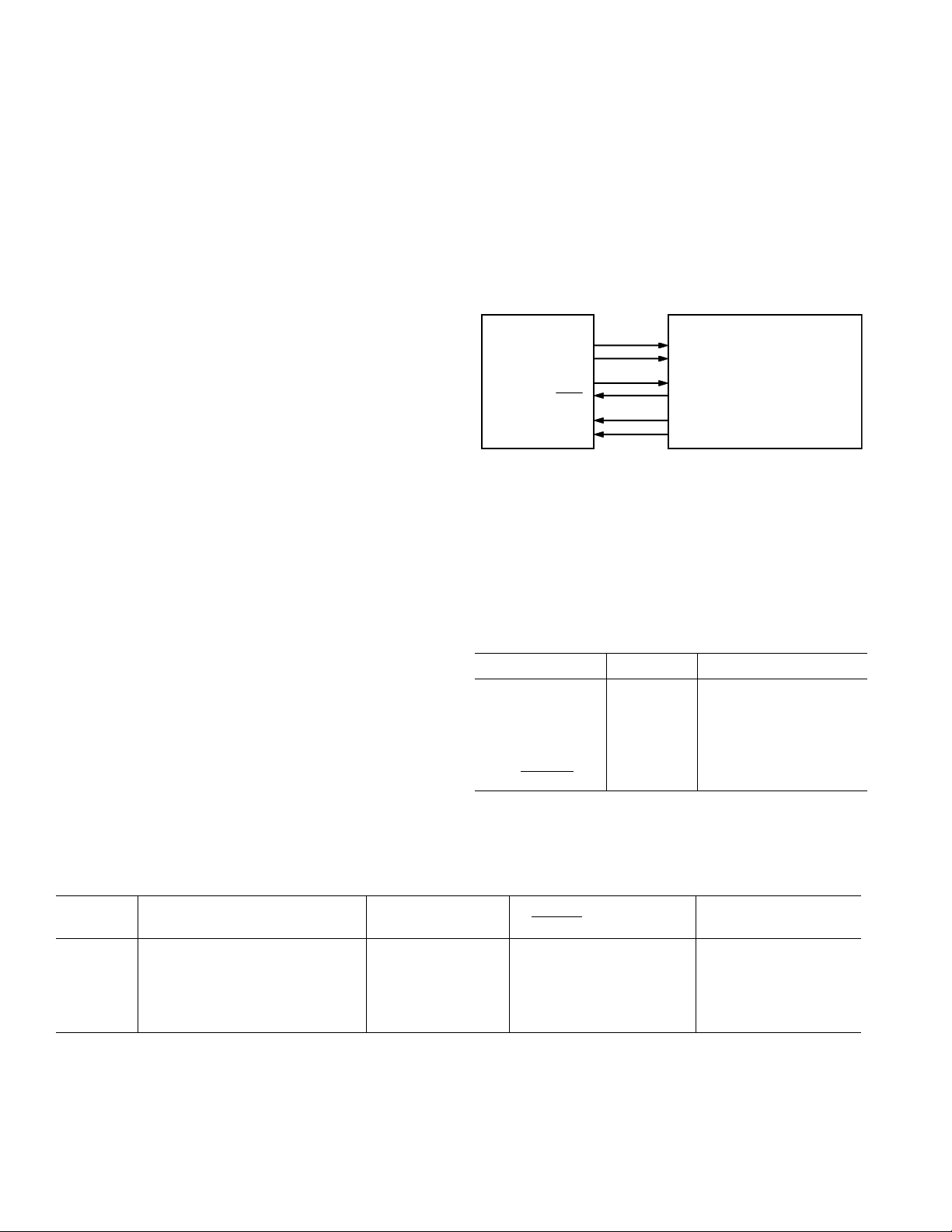
Host Processor Interface
The AD28msp02-to-host processor interface is shown in Figure 4.
Figure 4. AD28msp02-to-Host Processor Interface
Table I describes the SPORT signals and how they are used to
communicate with the host processor. The AD28msp02’s chip
select (CS) must be held high to enable SPORT operation. CS
can be used to 3-state the SPORT pins and disable communication with the host processor.
To use the ADSP-2101 or ADSP-2111 as host DSP processor
for the AD28msp02, the following connections can be used (as
shown in Figure 5):
AD28msp02 Pin ADSP-2101/2111 Pin
SCLK – SCLK0
SDO – DR0
SDOFS – RFS0
SDI – DT0
SDIFS – TFS0
DATA/CNTRL – FO (Flag Output)
Signal Signal State When Signal State During
Name Description Generated By RESET Low (CS High) Powerdown (CS High)
SCLK Serial clock AD28msp02 Low Active
SDO Serial data output AD28msp02 Low Active*
SDOFS Serial data output frame sync AD28msp02 Low Low
SDI Serial data input Host Processor — —
SDIFS Serial data input frame sync Host Processor — —
(CS must be held high to enable SPORT operation.)
*Outputs last data value that was valid prior to entering powerdown.
Table I. SPORT Signals
–4–
REV. 0

Note that the ADSP-2101’s SPORT0 communicates with the
SDO
SDOFS
SCLK
DATA/CNTRL
SDI
SDIFS
AD28msp02
DR0
RFS0
SCLK0
FO
DT0
TFS0
ADSP-2101
AD28msp02’s SPORT while the ADSP-2101’s Flag Output
(FO) is used to signal the AD28msp02’s DATA/
CNTRL input.
SPORT1 on the ADSP-2101 must be configured for flags and
interrupts in this system.
Figure 6 shows an ADSP-2101 assembly language program that
initializes the AD28msp02 and implements digital loopback
through the DSP processor.
{ This ADSP-2101 program initializes the AD28msp02 }
{ and executes a loopback, or talk-through, routine. }
.MODULE/ABS = 0/BOOT = 0 test1;
resetv: JUMP begin; {restart}
RTI; RTI; RTI;
irq2v: RTI; RTI; RTI; RTI; {IRQ2}
st0x: RTI; RTI; RTI; RTI; {SPORT0 Tx}
sr0x: ax0 = rx0; {SPORT0 Rx}
tx0 = ax0;
RTI; RTI;
irq1v: RTI; RTI; RTI; RTI; {irq1}
irq0v: RTI; RTI; RTI; RTI; {irq0}
timerv: RTI; RTI; RTI; RTI;
begin: RESET FLAG
OUT;
AX0 = 0x2A0F; {Configure ADSP-2101 SPORT0 for }
DM (0x3FF6) = AX0; { ext. SCLK, ext. RFS, int. TFS }
AX0 = 0x101F; { Enable ADSP-2101 SPORT0, }
DM (0x3FFF) = AX0; { configure SPORT1 for Flag Out }
IMASK= 0x10;
AX0 = 0x30; { Write control word to take}
TX0 = AX0; { AD28msp02 out of powerdown }
IDLE;
NOP;
IMASK= 0x08;
SET FLAG
OUT;
wait: JUMP wait; { Wait for receive interrupt }
NOP;
.ENDMOD;
AD28msp02
Figure 5. AD28msp02-to-ADSP-2101 Interface
REV. 0
Figure 6. ADSP-2101 Digital Loopback Routine
–5–
AD28msp02
Serial Data Output
The AD28msp02’s SPORT will begin transmitting data to the
host processor at an 8 kHz rate when the PWDD and PWDA
bits (Bits 4, 5) of the control register are set to 1. In the program shown in Figure 6, the instructions
AX0 = 0x30; { Write control word to take }
TX0 = AX0; { AD28msp02 out of powerdown }
accomplish this by writing 0x30 to the AD28msp02’s control
register. There is a short start-up time (after the end of this control register write) before the AD28msp02 raises SDOFS and
begins transmitting data; see Figure 11.
At the 13 MHz MCLK frequency, data is transmitted at an
8 kHz rate with a single 16-bit word transmitted every 125 µs.
While data is being output, the AD28msp02 asserts SDOFS at
an 8 kHz rate. Each 16-bit word transfer begins one serial clock
cycle after SDOFS is asserted.
Serial Data Input
The host processor must initiate data transfers to the
AD28msp02 by asserting the serial data input frame sync
(SDIFS) high. The 16-bit word transfer begins one serial clock
cycle after SDIFS is asserted. The DATA/CNTRL line must be
driven high when SDIFS is driven high.
The host processor must assert SDIFS shortly after the rising
edge of SCLK and must maintain SDIFS high for one cycle.
Data is then driven from the host processor (to the SDI input)
shortly after the rising edge of the next SCLK and is clocked
into the AD28msp02 on the falling edge of SCLK in that cycle.
Each bit of a 16-bit data word is thus clocked into the
AD28msp02 on the falling edge of SCLK (MSB first).
If SDIFS is asserted high again before the end of the present
data word transfer, it is not recognized until the falling edge of
SCLK in the last (LSB) cycle.
(Note: Exact SPORT timing requirements are defined in the
“Specifications” section of this data sheet.)
CONTROL REGISTER
The AD28msp02’s control register configures the device for
various modes of operation including ADC and DAC gain settings, ADC input mux selection, filter bypass, and powerdown.
The AD28msp02’s host processor can read and write to the
control register through the AD28msp02’s serial port (SPORT)
by driving the DATA/
The control register is cleared (set to 0x0000) when the
AD28msp02 is reset.
Control Register Writes
To write the control register, the host processor must assert
DATA/
CNTRL low when it asserts SDIFS. If the MSB of
the bit stream is also low, the SPORT recognizes the incoming
serial data as a new control word and copies it to the
AD28msp02’s control register. The format for the control word
write is shown in Table II; reserved Bits 10-15 must be set to
zero.
CNTRL pin low.
Table II. Control Word Write Format
15 14 13 12 11 10 9 8 7 6 5 4 3 2 1 0
0 0 0 0 0 0 OG2 OG1 OG0 0 PWDD PWDA ADBY DABY IMS IPS
0 IPS Analog input preamplifier select: 1 = insert (+20 dB), 0 = bypass (0 dB)
1 IMS Analog input multiplexer select: 1 = AUX input, 0 = NORM input
2 DABY DAC high-pass filter bypass select: 0 = insert, 1 = bypass
3 ADBY ADC high-pass filter bypass select: 0 = insert, 1 = bypass
4 PWDA Powerdown analog: 0 = powerdown, 1 = operating
5 PWDD Powerdown digital: 0 = powerdown, 1 = operating
7–9 OG2-OG0 Analog output gain setting (for D/A output PGA)
10–15 Reserved
Gain OG2 OG1 OG0
+6 dB 0 0 0
+3 dB 0 0 1
0 dB 0 1 0
–3 dB 0 1 1
–6 dB 1 0 0
–9 dB 1 0 1
–12 dB 1 1 0
–15 dB 1 1 1
Gain settings are accurate within ±0.6 dB.
(Control Register is set to 0x0000 at RESET. Reserved Bits
10–15 must be set to 0 for all Control Register writes.)
–6–
REV. 0

AD28msp02
MUX
VOLTAGE
REFERENCE
VFB
VFB
VIN
AD28msp02
VIN
NORM
AUX
NORM
AUX
C
FB
C
IN
R
IN
R
FB
INPUT
SIGNAL
Table III. Control Word Read Format
Read Request
15 14 13 12 11 10 9 8 7 6 5 4 3 2 1 0
100 0 0 0 00 0 00 0 0 000
Read Ready
15 14 13 12 11 10 9 8 7 6 5 4 3 2 1 0
110 0 0 0 00 0 00 0 0 000
Control Register Reads
To read the control register, the host processor must transfer
two control words. For each transfer, the DATA/
CNTRL pin
must be low when SDIFS is asserted. If the MSB of the bit
stream is high, the SPORT recognizes the incoming serial data
as a request for control information. The protocol for reading
the control register is as follows:
1. The host processor sends a “Read Request” control word to
the AD28msp02. Since the MSB of this control word is high,
the SPORT recognized the incoming serial data as a read request and does not overwrite the control register.
2. When the AD28msp02 receives the read request, it finishes
any data transfers in progress and waits for a “Read Ready”
control word.
3. The host processor then transfers a “Read Ready” control
word to the AD28msp02. Upon receiving this control word,
the AD28msp02 transfers the control register contents to the
host processor via the SPORT.
4. When the SPORT completes the control register transfer, it
immediately resumes transmitting data at an 8 kHz rate.
This scheme allows any data transfers in progress to be completed and resolves any ambiguities between data and control
words. The format for the read control words is shown in
Table III.
In the circuit shown in Figure 7, scaling of the analog input is
achieved by the resistors R
–R
, can be adjusted from –12 dB to +26 dB by varying
FB/RIN
and RFB. The input signal gain,
IN
the values of these resistors. The AD28msp02’s on-chip 20 dB
preamplifier can be enabled when there is not enough gain in
the input circuit; the preamplifier is configured by Bit 0 (IPS) of
the control register. Total gain must be configured to ensure
that a full-scale input signal (at C
in Figure 7) produces a sig-
IN
nal level at the input to the sigma-delta modulator of the ADC
that does not exceed V
, which is specified under “Analog
INMAX
Interface Electrical Characteristics.” If the total gain is increased
above unity, signal-to-noise (SNR + THD) performance will
not meet the listed specifications.
DESIGN CONSIDERATIONS
Analog Input
The analog input signal to the AD28msp02 must be ac-coupled.
Figure 7 shows the recommended input circuit for the
AD28msp02’s analog input pin (either VIN
NORM
or VIN
AUX
The circuit of Figure 7 implements a first-order low-pass filter
with a 3 dB point at 20 kHz; this is the only filter that must be
implemented external to the AD28msp02 to prevent aliasing of
the sampled signal. Since the AD28msp02’s ADC uses a highly
oversampled approach that transfers the bulk of the anti-aliasing
filtering into the digital domain, the off-chip anti-aliasing filter
need only be of low order.
REV. 0
).
Figure 7. Recommended Analog Input Circuit
The dc biasing of the analog input signal is accomplished with
an on-chip voltage reference which nominally equals 2.5 V. The
input signal must be ac-coupled with an external coupling capacitor (C
pling corner frequency of 30 Hz. C
). CIN and RIN should be chosen to ensure a cou-
IN
should be 0.1 µF or larger.
IN
–7–

AD28msp02
C
OUT
C
OUT
VOUT
P
VOUT
N
R
L
AD28msp02
SSM2141
1
5
7
4
+12 V
0.1 µF
0.1 µF
–12 V
V
OUT
AD28msp02
VOUT
P
VOUT
N
GND
A
GND
A
GND
A
To select values for the components shown in Figure 7, use the
following equations:
R
R
1
60 π R
1
FB
IN
IN
3
) R
FB
10 kΩ ≤ R
150 pF ≤ C
, R
FB
IN
≤ 600 pF
FB
CIN=
CFB=
≤ 50 kΩ
Gain =
(2 π)( 20 × 10
Figure 8 shows an example of a typical input circuit configured
for 0 dB gain. The circuit’s diodes are used to prevent the input
signal from exceeding maximum limits.
A
10k
330pF
VFB
NORM
20k
Ω
Ω
VIN
VFB
VIN
NORM
AUX
AUX
MUX
INPUT
SIGNAL
1.0µF
10k
V
Ω
GND
CC
Figure 9 shows a simple circuit providing a differential output
with ac coupling. The capacitor of this circuit (C
OUT
) is
optional; if used, its value can be chosen as follows:
=
(60 π) R
1
L
C
OUT
Figure 9. Example Circuit for Differential Output
The VOUTP–VOUTN outputs must be used as differential outputs; do not use either as a single-ended output. Figure 10
shows an example circuit which can be used to convert the differential output to a single-ended output. The circuit uses a
differential-to-single-ended amplifier, the Analog Devices
SSM2141.
VOLTAGE
REFERENCE
AD28msp02
Figure 8. Example Analog Input Circuit for 0 dB Gain
Analog Output
The AD28msp02’s differential analog output (VOUTP, VOUTN)
is produced by an on-chip differential amplifier. The differential
amplifier can drive a minimum load of 2 kΩ (R
≥ 2 kΩ) and
L
has a maximum differential output voltage swing of ±3.156 V
peak-to-peak (3.17 dBm0). The differential output can be
ac-coupled directly to a load or dc-coupled to an external
amplifier.
Figure 10. Example Circuit for Single-Ended Output
–8–
REV. 0

AD28msp02
Serial Output Startup Time
The AD28msp02 begins transmitting data to the host processor
after it is taken out of powerdown. To take the AD28msp02 out
of powerdown, the host processor writes a control word to the
AD28msp02.
The start-up time (from the start of this control word write)
before the AD28msp02 begins transmitting data is shown in
Figure 11.
PC Board Layout Considerations
Separate analog and digital ground planes should be provided
for the AD28msp02 in order to ensure the characteristics of the
device’s ADC and DAC. The two ground planes should be connected at a single point—this is often referred to as a “Star” or
“Mecca” grounding configuration. The point of connection may
be at the system power supply, at the PC board power connection, or at any other appropriate location. Because ground loops
increase susceptibility to EMF, multiple connections between
the analog and digital ground planes should be avoided.
The ground planes should be designed such that all noisesensitive areas are isolated from one another and critical signal
SCLK
DATA/
CNTRL
SDIFS
traces (such as digital clocks and analog signals) are as short as
possible.
Each +5 V digital supply pin, V
, of the AD28msp02 (SOIC
DD
Pins 20, 21) should be bypassed to ground with a 0.1 µF capaci-
tor. These capacitors should be low inductance, monolithic, ceramic, and surface-mount. The capacitor leads and PC board
traces should be as short as possible to minimize inductive effects. In addition, a 10 µF capacitor should be connected be-
tween V
and ground, near the PC board power connection.
DD
MCLK Frequency
The sigma-delta converters and digital filters of the AD28msp02
are specifically designed to operate at a master clock (MCLK)
frequency of 13.0 MHz. MCLK must equal 13.0 MHz to guarantee the filter characteristics and sample rate of the ADC and
DAC. The AD28msp02 is not tested or characterized at any
other clock frequency.
A low cost crystal with a different frequency, for example
12.288 MHz, can be used for the master clock input; in this
case, however, the AD28msp02 is not guaranteed to meet the
specifications listed in this data sheet.
SDI
SDOFS
SDO
MSB
POWERUP CONTROL WORD
WRITTEN TO AD28msp02
(2050 MCLK CYCLES)
2nd MSB
410 SCLK CYCLES
Figure 11. Serial Output Startup Time
MSB
FIRST DATA WORD
FROM AD28msp02
2nd MSB
TRANSMITTED
REV. 0
–9–

AD28msp02
DEFINITION OF SPECIFICATIONS
Absolute Gain
Absolute gain is a measure of converter gain for a known signal.
Absolute gain is measured with a 1.0 kHz sine wave at 0 dBm0.
The absolute gain specification is used as a reference for gain
tracking error specification.
Gain Tracking Error
Gain tracking error measures changes in converter output for
different signal levels relative to an absolute signal level. The absolute signal level is 1 kHz at 0 dBm0 (equal to absolute gain).
Gain tracking error at 0 dBm0 is 0 dB by definition.
SNR + THD
Signal-to-noise ratio plus total harmonic distortion is defined to
be the ratio of the rms value of the measured input signal to the
rms sum of all other spectral components in the frequency range
300 Hz–3400 Hz, including harmonics but excluding dc.
Intermodulation Distortion
With inputs consisting of sine waves at two frequencies, fa and
fb, any active device with nonlinearities will create distortion
products at sum and difference frequencies of mfa ± nfb where
m, n = 0, 1, 2, 3, etc. Intermodulation terms are those for which
neither m or n are equal to zero. For final testing, the second order terms include (fa + fb) and (fa – fb), while the third order
terms include (2fa + fb), (2fa – fb), (fa + 2fb), and (fa – 2fb).
Idle Channel Noise
Idle channel noise is defined as the total signal energy measured
at the output of the device when the input is grounded (measured in the frequency range 300 Hz–3400 Hz).
Crosstalk
Crosstalk is defined as the ratio of the amplitude of a full-scale
signal appearing on one channel to the amplitude of the same
signal which couples onto the adjacent channel. Crosstalk is expressed in dB.
Power Supply Rejection
Power supply rejection measures the susceptibility of a device to
noise on the power supply. Power supply rejection is measured
by modulating the power supply with a sine wave and measuring
the noise at the output (relative to 0 dB).
Group Delay
Group delay is defined as the derivative of radian phase with respect to radian frequency, ∂φ(ω)/∂ω. Group delay is a measure
of average delay of a system as a function of frequency. A linear
system with a constant group delay has a linear phase response.
The deviation of group delay away from a constant indicates the
degree of nonlinear phase response of the system.
–10–
REV. 0

AD28msp02
WARNING!
ESD SENSITIVE DEVICE
SPECIFICATIONS
RECOMMENDED OPERATING CONDITIONS
K Grade B Grade
Parameter Min Max Min Max Unit
VDD, V
CC
T
AMB
Refer to Environmental Conditions for information on case temperature and thermal specifications.
ABSOLUTE MAXIMUM RATINGS*
Supply Voltage 4.50 5.50 4.50 5.50 V
Ambient Operating Temperature 0 +70 –40 +85 °C
Supply Voltage . . . . . . . . . . . . . . . . . . . . . . . . . . –0.3 V to +7 V
Input Voltage . . . . . . . . . . . . . . . . . . . . . –0.3 V to V
Output Voltage Swing . . . . . . . . . . . . . . –0.3 V to V
+ 0.3 V
DD
+ 0.3 V
DD
Operating Temperature Range (Ambient) . . . –40°C to +85°C
Storage Temperature Range . . . . . . . . . . . . . –55°C to +150°C
Lead Temperature (5 sec) SOIC . . . . . . . . . . . . . . . . . +280°C
*Stresses above those listed under “Absolute Maximum Ratings” may cause
permanent damage to the device. These are stress rating only and functional
operation of the device at these or any other conditions above those indicated in the
operational sections of this specification is not implied. Exposure to absolute
maximum rating conditions for extended periods may affect device reliability.
ESD SENSITIVITY
The AD28msp02 features proprietary input protection circuitry to dissipate high-energy discharges
(Human Body Model). Per method 3015 of MIL-STD-883C, the AD28msp02 has been classified as
a Class 1 device.
Proper ESD precautions are strongly recommended to avoid functional damage or performance
degradation. Charges readily accumulate on the human body and test equipment and discharge without
detection. Unused devices must be stored in conductive foam or shunts, and the foam should be
discharged to the destination socket before devices are removed.
REV. 0
–11–

AD28msp02
DIGITAL INTERFACE ELECTRICAL CHARACTERISTICS
Symbol Parameter Min Typ Max Unit Test Condition
V
V
V
V
I
IH
I
IL
I
OZL
I
OZH
C
IH
IL
OH
OL
I
Input High Voltage 2.4 V VDD = max
Input Low Voltage 0.8 V VDD = min
Output High Voltage 2.4 V VDD = min, IOH = –0.5 mA
Output Low Voltage 0.4 V VDD = min, IOL = 2 mA
High Level Input Current 10 µAV
Low Level Input Current 10 µAV
Low Level Output 3-State Leakage Current 10 µAV
High Level Output 3-State Leakage Current 10 µAV
= max, VIN = max
DD
= max, VIN = 0 V
DD
= max, VIN = max
DD
= max, VIN = 0 V
DD
Digital Input Capacitance 10 pF
ANALOG INTERFACE ELECTRICAL CHARACTERISTICS
Symbol Parameter Min Typ Max Unit
ADC:
I
L
R
I
C
IL
VIN
DAC:
R
O
V
OOFF
C
OL
V
VREF
V
O
MAX
Input Leakage Current at VIN
Input Resistance1 at VIN
Input Load Capacitance1 at VIN
Maximum Input Range
Output Resistance
Output DC Offset
Output Load Capacitance
Voltage Reference (V
NORM
2
1, 3
4
3
) 2.25 2.75 V
REF
Maximum Voltage Output Swing (p-p) Across R
NORM
, VIN
NORM
, VIN
AUX
, VIN
AUX
AUX
L
10 nA
100 MΩ
10 pF
3.156 V p-p
1 Ω
400 mV
100 pF
Single-Ended 3.156 V
Differential 6.312 V
R
L
Test Conditions for all analog interface tests: Unity input gain, A/D 20 dB preamplifier bypassed, D/A PGA set for 0 dB gain, no load on analog output
(VOUTP–VOUTN).
1
Guaranteed but not tested.
2
At input to sigma-delta modulator of ADC.
3
At VOUTP-VOUTN.
4
Between VOUTP and VOUTN.
Load Resistance
3
2kΩ
POWER DISSIPATION
Symbol Parameter Min Max Unit
V
CC
V
DD
I
DD
P
1
I
DD
P
0
Test conditions: VDD = VCC = 5.0 V, MCLK frequency 13.0 MHz, no load on digital pins, analog inputs ac-coupled to ground, no load on analog output
(VOUTP–VOUTN)
I
Active: AD28msp02 operational (PWDD and PWDA set to 1 in control register).
2
Inactive: AD28msp02 in powerdown state (PWDD and PWDA set to 0 in control register) and MCLK tied to VDD.
Analog Operating Voltage 4.5 5.5 V
Digital Operating Voltage 4.5 5.5 V
Operating Current Active
Power Dissipation Active
Operating Current Inactive
Power Dissipation Inactive
1
1
2
2
40 mA
200 mW
0.5 mA
2.5 mW
–12–
REV. 0

AD28msp02
TIMING PARAMETERS
Clock Signals
Parameter Min Max Unit
Timing Requirement:
t
MCK
t
MKL
t
MKH
Switching Characteristic:
t
SCK
t
SKL
t
SKH
MCLK Period 76.9 76.9 ns
MCLK Width Low 0.5t
MCLK Width High 0.5t
SCLK Period 5t
SCLK Width Low 3t
SCLK Width High 2t
– 10 0.5t
MCK
– 10 0.5t
MCK
MCK
– 10 3t
MCK
– 10 2t
MCK
t
MCK
+ 10 ns
MCK
+ 10 ns
MCK
+ 10 ns
MCK
+ 10 ns
MCK
ns
MCLK
SCLK
t
MKL
t
SCK
t
SKL
t
MKH
t
SKH
Figure 12. Clock Signals
Serial Port 3-State
Parameter Min Max Unit
Switching Characteristic:
t
t
t
SPD
SPE
SPV
CS Low to SDO, SDOFS, SCLK Disable 25 ns
CS High to SDO, SDOFS, SCLK Enable 0 ns
CS High to SDO, SDOFS, SCLK Valid 10 ns
CS
SDO
SDOFS
SCLK
t
SPD
t
SPE
t
SPV
REV. 0
Figure 13. Serial Port 3-State
–13–

AD28msp02
Serial Ports
Parameter Min Max Unit
Timing Requirements:
t
SCS
t
SCH
t
DCS
t
DCH
Switching Characteristic:
t
RD
t
RH
t
SCDH
t
SCDD
DATA/CNTRL
SDI/SDIFS Setup before SCLK Low 10 ns
SDI/SDIFS Hold after SCLK Low 10 ns
DATA/CNTRL Setup before SCLK Low 10 ns
DATA/CNTRL Hold after SCLK Low 10 ns
SDOFS Delay from SCLK High 15 ns
SDOFS Hold after SCLK High 0 ns
SDO Hold after SCLK High 0 ns
SDO Delay from SCLK High 30 ns
t
SCK
SCLK
t
SCS
SDIFS
t
SCH
t
DCS
t
DCH
t
SCH
SDI
SDOFS
SDO
MSB
t
RD
t
SCDD
Figure 14. Serial Ports
t
t
RH
2ND MSB
SCS
3RD MSB
t
SCDH
–14–
REV. 0

AD28msp02
DIGITAL TEST CONDITIONS
3.0V
1.5V
2.0V
1.5V
0.8V
0.0V
DIGITAL INPUT
DIGITAL OUTPUT
Figure 15. Voltage Reference Levels for AC Measurements
TO DIGITAL
OUTPUT PIN
50pF
I
OL
I
OH
+1.5V
Figure 16. Equivalent Device Loading for AC
Measurements (Includes All Fixtures)
GAIN
Parameter Min Typ Max Unit Test Conditions
ADC Absolute Gain –0.2 0 0.2 dBm0 1.0 kHz, 0 dBm0
ADC Gain Tracking Error –0.1 0 0.1 dBm0 1.0 kHz, +3 to –50 dBm0
DAC Absolute Gain –0.2 0 0.2 dBm0 1.0 kHz, 0 dBm0
DAC Gain Tracking Error –0.1 0 0.1 dBm0 1.0 kHz, +3 to –50 dBm0
FREQUENCY RESPONSE
Input Freq Min Output Max Output
(Hz) (dB) (dB)
0–∞–25
100 –∞ –25
150 –0.3 +0.3
200 –0.3 +0.3
300 –0.2 +0.2
1000 –0.2 +0.2
2000 –0.2 +0.2
3000 –0.2 +0.2
3400 –0.2 +0.2
3700 –0.3 +0.3
4000 –∞ –60
>4000 –∞ –60
Frequency responses of ADC and DAC measured with input at audio reference
level (the input level that produces an output level of –10 dBm0), with 20 dB
preamplifier bypassed and input gain of 0 dB. The in-band ripple shall not exceed 0.2 dB.
REV. 0
–15–

AD28msp02
NOISE AND DISTORTION
Parameter Min Max Unit Test Conditions
ADC Intermodulation Distortion –70 dB
DAC Intermodulation Distortion –70 dB
ADC Idle Channel Noise 72 dBm0
DAC Idle Channel Noise 72 dBm0
ADC Crosstalk –65 dB ADC input signal level: 1.0 kHz, 0 dBm0
DAC input at idle
DAC Crosstalk –65 dB ADC input signal level: analog ground
DAC output signal level: 1.0 kHz, 0 dBm0
ADC Power Supply Rejection –55 dB Input signal level at V
1.0 kHz, 100 mV p-p sine wave
DAC Power Supply Rejection 55 dB Input signal level at V
ADC Group Delay
DAC Group Delay
1
Guaranteed but not tested.
1
1
1 ms 300–3000 Hz
1 ms 300–3000 Hz
70
60
50
1.0 kHz, 100 mV p-p sine wave
and VDD pins:
CC
and VDD pins:
CC
40
30
20
SNR+THD – dB
10
0
–10
–55–60
Figure 17. SNR + THD vs. V
V – dBm0
IN
0
–5–10–15–25–30–35–40–45–50 –20
3.17
IN
ORDERING GUIDE
Part Temperature Package
Number Range Package Option*
AD28msp02KN 0°C to +70°C 24-Pin Plastic DIP N-24
AD28msp02KR 0°C to +70°C 28-Lead SOIC R-28
AD28msp02BN –40°C to +85°C 24-Pin Plastic DIP N-24
AD28msp02BR –40°C to +85°C 28-Lead SOIC R-28
*N = Plastic DIP, R = Small Outline (SOIC).
–16–
REV. 0

PIN CONFIGURATIONS
24-Pin Plastic DIP
V
1
CC
2
V
REF
VOUT
3
P
VOUT
4
N
5
GND
A
6
GND
D
AD28msp02
SDO
SDOFS
SDI
SDIFS
SCLK
7
8
9
10
11
12
TOP VIEW
(Not to Scale)
DATA/CNTRL
NC = NO CONNECTION
28-Lead SOIC
V
1
CC
2
V
REF
3
VOUT
P
VOUT
4
N
5
GND
A
GND
6
A
D
D
SDO
SDI
AD28msp02
7
TOP VIEW
(Not to Scale)
8
9
10
11
12
13
14
GND
GND
DATA/CNTRL
SDOFS
SDIFS
SCLK
AD28msp02
24
VIN
NORM
23
VFB
NORM
22
VIN
AUX
21
VFB
AUX
20
GND
A
19
GND
D
V
18
DD
17
NC
16
NC
15
RESET
CS
14
MCLK
13
28
VIN
NORM
27
VFB
NORM
26
VIN
AUX
VFB
25
AUX
GND
24
A
23
GND
D
22
GND
D
21
V
DD
20
V
DD
19
NC
18
NC
17
RESET
16
CS
MCLK
15
REV. 0
NC = NO CONNECTION
–17–

AD28msp02
OUTLINE DIMENSIONS
Dimensions shown in inches and (mm).
24-Pin Plastic DIP
(N-24)
0.200 (5.05)
0.125 (3.18)
PIN 1
PIN 1
0.210
(5.33)
MAX
0.022 (0.558)
0.014 (0.356)
28
1
24
1
1.275 (32.30)
1.125 (28.60)
0.100
(2.54)
BSC
0.070 (1.77)
0.045 (1.15)
28-Lead Wide-Body SOIC
(R-28)
15
0.2992 (7.60)
0.2914 (7.40)
14
0.7125 (18.10)
0.6969 (17.70)
0.1043 (2.65)
0.0926 (2.35)
13
0.280 (7.11)
0.240 (6.10)
12
0.060 (1.52)
0.015 (0.38)
0.150
(3.81)
MIN
SEATING
PLANE
0.4193 (10.65)
0.3937 (10.00)
0.325 (8.25)
0.300 (7.62)
0.015 (0.381)
0.008 (0.204)
0.0291 (0.74)
0.0098 (0.25)
0.195 (4.95)
0.115 (2.93)
x 45
°
0.0118 (0.30)
0.0040 (0.10)
0.0500 (1.27)
BSC
0.0192 (0.49)
0.0138 (0.35)
0.0125 (0.32)
0.0091 (0.23)
0.0500 (1.27)
8
°
0.0157 (0.40)
0
°
–18–
REV. 0

–19–

C1672–8–6/92
–20–
PRINTED IN U.S.A.
 Loading...