

Linear Output
NC
R1
GND
R3
R2
V
CC
AD22151
NC = NO CONNECT
OUTPUT
0.1F
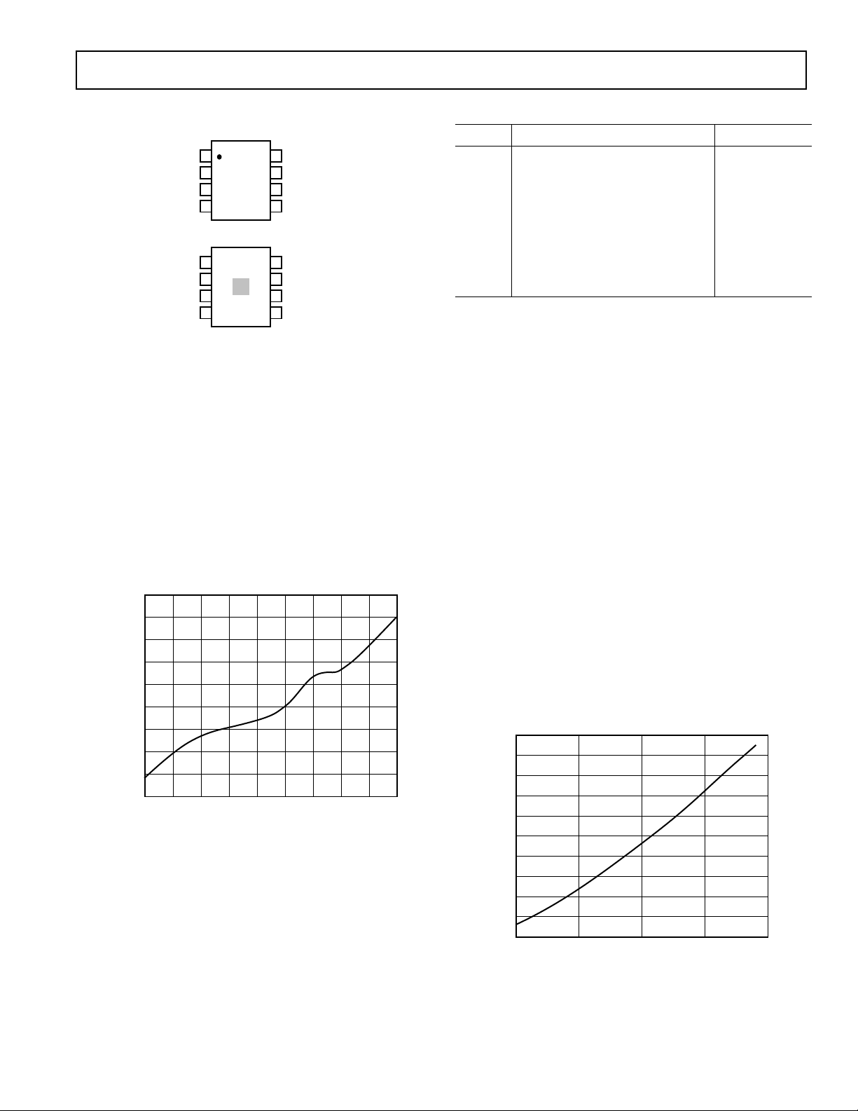
NC
R1
GND
R3
R2
V
CC
AD22151
NC = NO CONNECT
OUTPUT
0.1F
R4
a
FEATURES
Adjustable Offset to Unipolar or Bipolar Operation
Low Offset Drift Over Temperature Range
Gain Adjustable Over Wide Range
Low Gain Drift Over Temperature Range
Adjustable First Order Temperature Compensation
Ratiometric to V
APPLICATIONS
Automotive
Throttle Position Sensing
Pedal Position Sensing
Suspension Position Sensing
Valve Position Sensing
Industrial
Absolute Position Sensing
Proximity Sensing
GENERAL DESCRIPTION
The AD22151 is a linear magnetic field transducer. The sensor
output is a voltage proportional to a magnetic field applied
perpendicularly to the package top surface.
The sensor combines integrated bulk Hall cell technology and
instrumentation circuitry to minimize temperature related drifts
associated with silicon Hall cell characteristics. The architecture
maximizes the advantages of a monolithic implementation while
allowing sufficient versatility to meet varied application requirements with a minimum number of components.
Principle features include dynamic offset drift cancellation and a
built-in temperature sensor. Designed for single +5 volt supply
operation, the AD22151 achieves low drift offset and gain operation over –40°C to +150°C. Temperature compensation can
accommodate a number of magnetic materials commonly utilized in economic position sensor assemblies.
The transducer may be configured for specific signal gains dependent upon application requirements. Output voltage can be
adjusted from fully bipolar (reversible) field operation to fully
unipolar field sensing.
The voltage output achieves near rail-to-rail dynamic range,
capable of supplying 1 mA into large capacitive loads. The signal is ratiometric to the positive supply rail in all configurations.
CC
Magnetic Field Sensor
AD22151
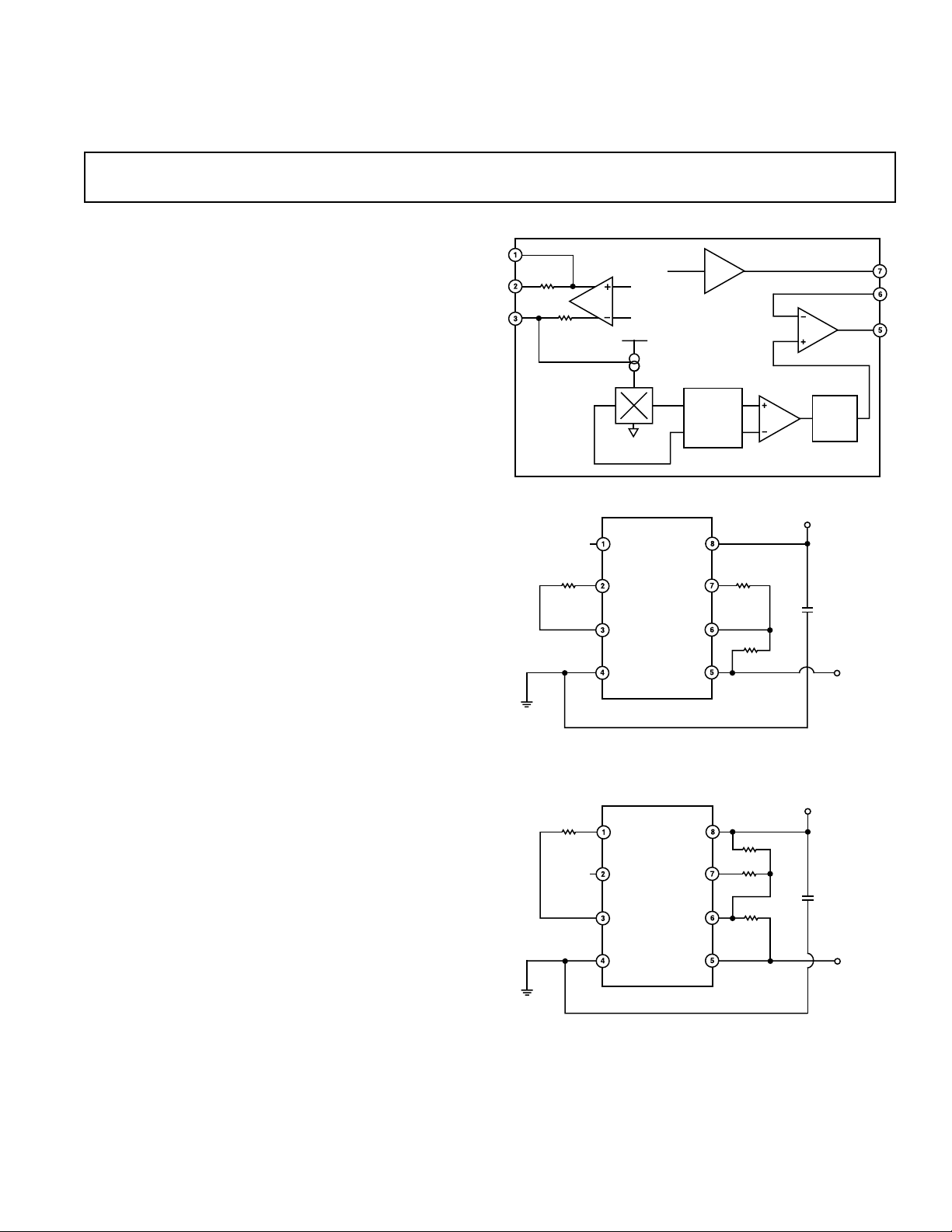
FUNCTIONAL BLOCK DIAGRAM
V
/2
CC
TEMP REF
AD22151
I
SOURCE
Figure 1. Typical Bipolar Configuration with Low
(< –500 ppm) Compensation
OUT AMP
DEMODSWITCHES
REF
REV. 0
Information furnished by Analog Devices is believed to be accurate and
reliable. However, no responsibility is assumed by Analog Devices for its
use, nor for any infringements of patents or other rights of third parties
which may result from its use. No license is granted by implication or
otherwise under any patent or patent rights of Analog Devices.
Figure 2. Typical Unipolar Configuration with High
(≈
–2000 ppm) Compensation
One Technology Way, P.O. Box 9106, Norwood, MA 02062-9106, U.S.A.
Tel: 781/329-4700 World Wide Web Site: http://www.analog.com
Fax: 781/326-8703 © Analog Devices, Inc., 1997
AD22151–SPECIFICATIONS
WARNING!
ESD SENSITIVE DEVICE
(TA = +25ⴗC and V+ = +5 V unless otherwise noted)
Parameters Min Typ Max Units
OPERATION
Operating 4.5 5.0 6.0 V
V
CC
ICC Operating 6.0 10 mA
INPUT
TC3 (Pin 3) Sensitivity/Volt 160 µV/G/V
V
Input Range
OUTPUT
1
2
CC
± 0.5 V
2
Sensitivity (External Adjustment, Gain = 1) 0.4 mV/G
Linear Output Range 10 90 % of V
Output Min 5 % of V
Output Max (Clamp) 93 % of V
CC
CC
CC
Drive Capability 1.0 mA
V
Offset @ 0 Gauss
Offset Adjust Range 5 95 % of V
CC
2
V
CC
Output Short Circuit Current 5.0 mA
ACCURACIES
Nonlinearity (10% to 90% Range) 0.1 % FS
Gain Error (Over Temperature Range) ±1%
Offset Error (Over Temperature Range) ±6.0 G
Uncompensated Gain TC (G
RATIOMETRICITY ERROR 1 %V/V
) 950 ppm
TCU
CC
3 dB ROLL-OFF (5 mV/G) 5.7 kHz
OUTPUT NOISE FIGURE (6 kHz BW) 2.4 mV/rms
PACKAGE 8-Lead SOIC
OPERATING TEMPERATURE RANGE –40 +150 °C
NOTES
1
–40°C to +150°C.
2
RL = 4.7 kΩ.
Specifications subject to change without notice.
ABSOLUTE MAXIMUM RATING*
Supply Voltage . . . . . . . . . . . . . . . . . . . . . . . . . . . . . . . . . 12 V
Package Power Dissipation . . . . . . . . . . . . . . . . . . . . . 25 mW
Storage Temperature . . . . . . . . . . . . . . . . . . –50°C to +160°C
Output Sink Current, I
. . . . . . . . . . . . . . . . . . . . . . . 15 mA
O
Model Range Description Option
AD22151YR –40°C to +150°C 8-Lead SOIC SO-8
Temperature Package Package
Magnetic Flux Density . . . . . . . . . . . . . . . . . . . . . . Unlimited
Lead Temperature (Soldering 10 sec) . . . . . . . . . . . . .+300°C
*Stresses above those listed under Absolute Maximum Ratings may cause perma-
nent damage to the device. This is a stress rating only; the functional operation of
the device at these or any other conditions above those indicated in the operational
sections of this specification is not implied. Exposure to the absolute maximum
rating conditions for extended periods may affect device reliability.
CAUTION
ESD (electrostatic discharge) sensitive device. Electrostatic charges as high as 4000 V readily
accumulate on the human body and test equipment and can discharge without detection.
Although the AD22151 features proprietary ESD protection circuitry, permanent damage may
occur on devices subjected to high energy electrostatic discharges. Therefore, proper ESD
precautions are recommended to avoid performance degradation or loss of functionality.
–2–
ORDERING GUIDE
REV. 0
AD22151
TEMPERATURE – ⴗC
14
–4
–40
% GAIN
10 60 110 160
12
4
2
0
–2
10
6
8
–6
PIN CONFIGURATION
1
TC1
2
AD22151
TC2
TOP VIEW
3
TC3
(Not to Scale)
4
GND
AREA OF SENSITIVITY*
1
2
3
(Not to Scale)
4
* SHADED AREA REPRESENTS
MAGNETIC FIELD AREA OF
SENSITIVITY (20MILS ⴛ 20MILS)
•
POSITIVE B FIELD INTO TOP OF
PACKAGE RESULTS IN A POSITIVE
VOLTAGE RESPONSE
8
V
7
REF
6
GAIN
5
OUTPUT
8
7
6
5
CC
CIRCUIT OPERATION
The AD22151 consists of epi Hall plate structures located at
the center of the die. The Hall plates are orthogonally sampled
by commutation switches via a differential amplifier. The two
amplified Hall signals are synchronously demodulated to provide a resultant offset cancellation (see Figure 3). The demodulated signal passes through a noninverting amplifier to provide
final gain and drive capability. The frequency at which the
output signal is refreshed is 50 kHz.
0.005
0.004
0.003
0.002
0.001
0
OFFSET – Volts
–0.001
–0.002
–0.003
–0.004
140 –40120
100 80 60 40 20 0 –20
TEMPERATURE – ⴗC
Figure 3. Relative Quiescent Offset vs. Temperature
PIN FUNCTION DESCRIPTIONS
Pin No. Description Connection
1 Temperature Compensation 1 Output
2 Temperature Compensation 2 Output
3 Temperature Compensation 3 Input/Output
4 Ground
5 Output Output
6 Gain Input
7 Reference Output
8 Positive Power Supply
“valleys” of the silicon crystal. Mechanical force on the sensor
is attributable to package-induced stress. The package material
acts to distort the encapsulated silicon altering the Hall cell gain
by ±2% and G
Figure 4 shows the typical G
by ±200 ppm.
TCU
characteristic of the AD22151.
TCU
This is the observable alteration of gain with respect to temperature with Pin 3 (TC3) held at a constant 2.5 V (uncompensated).
If a permanent magnet source used in conjunction with the
sensor also displays an intrinsic TC (B
), it will require factor-
TC
ing into the total temperature compensation of the sensor
assembly.
Figures 5 and 6 represent typical overall temperature/gain performance for a sensor and field combination (B
= –200 ppm).
TC
Figure 5 is the total drift in volts over a –40°C to +150°C temperature range with respect to applied field. Figure 6 represents
typical percentage gain variation from +25°C. Figures 7 and 8
show similar data for a B
= –2000 ppm.
TC
TEMPERATURE DEPENDENCIES
The uncompensated gain temperature coefficient (G
TCU
) of the
AD22151 is the result of fundamental physical properties associated with silicon bulk Hall plate structures. Low doped Hall
plates operated in current bias mode exhibit a temperature
relationship determined by the action of scattering mechanisms
and doping concentration.
The relative value of sensitivity to magnetic field can be altered
by the application of mechanical force upon silicon. The mechanism is principally the redistribution of electrons throughout the
–3–REV. 0
Figure 4. Uncompensated Gain Variation (from +25°C) vs.
Temperature

AD22151
0.025
0.020
0.015
0.010
DELTA SIGNAL – Volts
0.005
0
–600 –400 –200 0 200 400 600
Figure 5. Signal Drift Over Temperature (–40°C to +150°C)
vs. Field (–200 ppm); +5 V Supply
FIELD – Gauss
2.0
1.8
1.6
1.4
1.2
1.0
0.8
% GAIN
0.6
0.4
0.2
0
–0.2
–40 10 60 110 160
TEMPERATURE – ⴗC
Figure 8. Gain Variation (from +25°C) vs. Temperature
Ω
(–2000 ppm Field; R1 = 12 k
)
0.25
0.20
0.15
0.10
% GAIN
0.05
0
–0.05
–40 10 60 110 160
TEMPERATURE – ⴗC
Figure 6. Gain Variation from +25°C vs. Temperature
(–200 ppm) Field; R1 –15 k
0.045
0.040
0.035
0.030
0.025
0.020
0.015
DELTA SIGNAL – Volts
0.010
0.005
0
–600 800
–800 –400 –200 0 200 400 600
Ω
FIELD – Gauss
Figure 7. Signal Drift Over Temperature (–40°C to +150°C)
vs. Field (–2000 ppm); +5 V Supply
TEMPERATURE COMPENSATION
The AD22151 incorporates a “thermistor” transducer that
detects relative chip temperature within the package. This
function provides a compensation mechanism for the various
temperature dependencies of the Hall cell and magnet combinations. The temperature information is accessible at Pins 1 and 2
(≈ +2900 ppm /°C) and Pin 3 (≈ –2900 ppm/°C) as represented
by Figure 9. The compensation voltages are trimmed to converge at V
/2 at +25°C. Pin 3 is internally connected to the
CC
negative TC voltage via an internal resistor (see Functional
Block Diagram). An external resistor connected between Pin 3
and Pins 1 or 2 will produce a potential division of the two complementary TC voltages to provide optimal compensation. The
aforementioned Pin 3 internal resistor provides a secondary TC
designed to reduce second order Hall cell temperature sensitivity.
1.0
0.8
0.6
0.4
0.2
0
–0.2
–0.4
VOLTS – Reference
–0.6
–0.8
–1.0
150 112 74 –2 –40
TC1, TC2 VOLTS
TC3 VOLTS
36
TEMPERATURE – ⴗC
Figure 9. TC1, TC2 and TC3 with Respect to Reference vs.
Temperature
The voltages present at Pins 1, 2 and 3 are proportional to the
supply voltage. The presence of the Pin 2 internal resistor
distinguishes the effective compensation ranges of Pins 1 and 2
(see temperature configuration in Figures 1 and 2, and typical
resistor values in Figures 10 and 11).
Variation occurs in the operation of the gain temperature
compensation for two reasons. First, the die temperature within
–4–
REV. 0

the package is somewhat higher than the ambient temperature
R1 – k⍀
800
DRIFT – ppm
600
–200
400
0
200
0 5 10 20 25
–400
–600
15 30 35 40 45 50
due to self-heating as a function of power dissipation. Second,
package stress effect alters the specific operating parameters of
the gain compensation, particularly the specific cross over
temperature of TC1, TC3 ( ≈ ±10°C).
CONFIGURATION AND COMPONENT SELECTION
There are three areas of sensor operation that require external
component selection. Temperature compensation (R1), signal
gain (R2
Temperature
If the internal gain compensation is used, an external resistor is
required to complete the gain TC circuit at Pin 3. A number of
factors contribute to the value of this resistor.
a. The intrinsic Hall cell sensitivity TC ≈ 950 ppm.
b. Package induced stress variation in a. ≈ ±150 ppm.
c. Specific field TC ≈ –200 ppm (Alnico), –2000 ppm
(Ferrite), 0 ppm (electromagnet) etc.
d. R1, TC.
The final value of target compensation also dictates the use of
either Pin 1 or Pin 2. Pin 1 is provided to allow for large negative field TC such as ferrite magnets, thus R1 would be connected to Pins 1 and 3.
Pin 2 uses an internal resistive TC to optimize smaller field
coefficients such as Alnico, down to 0 ppm coefficients when
only the sensor gain TC itself is dominant. The TC of R1 itself
will also effect the compensation and as such a low TC resistor
(±50 ppm) is recommended.
Figures 10 and 11 indicate R1 resistor values and their associated effectiveness for Pins 1 and 2 respectively. Note that the
indicated drift response in both cases incorporates the intrinsic
Hall sensitivity TC (B
For example, the AD22151 sensor is to be used in conjunction
with an Alnico material permanent magnet. The TC of such
magnets is ≈ –200 ppm (see Figures 5 and 6). Figure 11 indicates that a compensating drift of +200 ppm at Pin 3 requires a
nominal value of R1 = 18 kΩ (assuming negligible drift of R1
itself).
3000
1500
DRIFT – ppm
Figure 10. Typical Resistor Value R1 vs. (Pins 1 and 3)
Drift Compensation
and R3), and offset (R4).
).
TCU
3500
2500
2000
1000
500
0
0 5 10 20 25
15 30
R1 – k⍀
AD22151
Figure 11. Typical Resistor Value R1 (Pins 2 and 3) vs.
Drift Compensation
GAIN AND OFFSET
The operation of the AD22151 can be bipolar (i.e., 0 Gauss =
/2) or a ratiometric offset can be implemented to Position
V
CC
Zero Gauss point at some other potential (i.e., 0.25 V).
The gain of the sensor can be set by the appropriate R2 and R3
resistor values (see Figure 1) such that:
Gain =1+
However, if an offset is required to position the quiescent output at some other voltage then the gain relationship is modified
to:
Gain =1+
The offset that R4
Offset =
For example:
At V
= 5 V at room temperature, the internal gain of the
CC
sensor is approximately 0.4 mV/Gauss. If a sensitivity of 6 mV/
Gauss is required with a quiescent output voltage of 1 V, the
following calculations apply (see Figure 2 ).
A value for R3 would be selected that complied with the various
considerations of current and power dissipation, trim ranges (if
applicable), etc. For the purpose of example assume a value of
85 kΩ.
To achieve a quiescent offset of 1 V requires a value for R4 as:
V
CC
2
V
CC
Thus:
R4 =
The gain required would be 6/0.4 (mV/Gauss) = 15
–5–REV. 0
R3
R2
(R2R4)
(R3+ R4)
–1
= 0.375
–1
85 kΩ
0.375
× 0.4 mV /G
R3
×0. 4 mV /G
introduces is:
R3
× VCC–V
()
– 85 kΩ=141.666 kΩ
OUT
(1)
(2)
(3)
(4)
(5)

AD22151
(
)
Knowing the values of R3 and R4 from above, and noting Equation 2, the parallel combination of R2 and R4 required is:
85 kΩ
= 6. 071 kΩ
15 –1
()
Thus:
= 6.342 kΩ
R2 =
6.071 kΩ
1
1
–
141.666 kΩ
1
NOISE
The principle noise component in the sensor is thermal noise
from the Hall cell. Clock feedthrough into the output signal is
largely suppressed with application of a supply bypass capacitor.
Figure 12 shows the power spectral density (PSD) of the output
signal for a gain of 5 mV/Gauss. The effective bandwidth of the
sensor is approximately 5.7 kHz. This is shown by Figure 13
small signal bandwidth vs. gain. The PSD indicates an rms
noise voltage of 2.8 mV within the 3 dB bandwidth of the sensor. A wideband measurement of 250 MHz indicates 3.2 mV
rms (see Figure 14a).
In many position sensing applications bandwidth requirements
can be as low as 100 Hz. Passing the output signal through an
LP filter, for example 100 Hz, would reduce the rms noise voltage to ≈1 mV. A dominant pole may be introduced into the
output amplifier response by connection of a capacitor across
feedback resistor R3, as a simple means of reducing noise at the
expense of bandwidth. Figure 14b indicates the output signal of
a 5 mV/G sensor bandwidth limited to 180 Hz with a 0.01 µF
feedback capacitor.
Note: Measurements taken with 0.1 µF decoupling capacitor
between V
and GND at +25°C.
CC
7
6
5
4
3
FREQUENCY– kHz
2
1
0
123
3dB FREQ. (kHz)
456
GAIN – mV/GAUSS
Figure 13. Small-Signal Gain Bandwidth
TEK STOP: 25.0 kS/s
2
CH2 10.0mV
3ACQS
[
B
W
T
T
M2.00ms
[
CH2 PK-PK
19.2mV
Figure 14a. Peak-to-Peak Full Bandwidth (10 mV/Division)
TEK STOP: 25.0 kS/s
7ACQS
[
T
[
B MARKER X 64Hz
100
H
LOGMAG
5 dB
/div
1
H
START: 64 Hz
NOISE: PSD
8 mV/GAUSS
STOP: 25.6 kHz
RMS: 64
Figure 12. Power Spectral Density (5 mV/G)
Y: 3.351 H
–6–
CH2 PK-PK
4.4mV
2
CH2 10.0mV
B
W
T
M2.00ms
Figure 14b. Peak-to-Peak 180 Hz Bandwidth
(10 mV/Division)
REV. 0

TEMPERATURE – ⴗC
2.496
VOLTS
2.494
2.492
2.488
2.490
140 120 100 80 60 40 20
2.486
2.484
0 –40–20
GAIN = 3.78mV/G
0.06
0.05
0.04
0.03
0.02
0.01
0
% ERROR
–0.01
–0.02
–0.03
–0.04
–0.05
–600 –400 –200 0 200 400 600
FIELD – Gauss
AD22151
Figure 15. Integral Nonlinearity vs. Field
Figure 16. Absolute Offset Volts vs. Temperature
–7–REV. 0

AD22151
0.1574 (4.00)
0.1497 (3.80)
PIN 1
0.0098 (0.25)
0.0040 (0.10)
SEATING
OUTLINE DIMENSIONS
Dimensions shown in inches and (mm).
8-Lead SOIC
(SO-8)
0.1968 (5.00)
0.1890 (4.80)
85
0.0500 (1.27)
PLANE
0.2440 (6.20)
0.2284 (5.80)
41
BSC
0.0192 (0.49)
0.0138 (0.35)
0.0688 (1.75)
0.0532 (1.35)
0.0098 (0.25)
0.0075 (0.19)
0.0196 (0.50)
0.0099 (0.25)
8ⴗ
0.0500 (1.27)
0ⴗ
0.0160 (0.41)
C3213–8–10/97
ⴛ 45ⴗ
–8–
PRINTED IN U.S.A.
REV. 0
 Loading...