

Voltage Output Temperature Sensor
FEATURES
200°C temperature span
Accuracy better than ±2% of full scale
Linearity better than ±1% of full scale
Temperature coefficient of 22.5 mV/°C
Output proportional to temperature × V+
Single-supply operation
Reverse voltage protection
Minimal self-heating
High level, low impedance output
APPLICATIONS
HVAC systems
System temperature compensation
Board level temperature sensing
Electronic thermostats
MARKETS
Industrial process control
Instrumentation
Automotive
GENERAL DESCRIPTION
The AD221001 is a monolithic temperature sensor with on-chip
signal conditioning. It can be operated over the temperature
range −50°C to +150°C, making it ideal for use in numerous
HVAC, instrumentation, and automotive applications.
with Signal Conditioning
FUNCTIONAL BLOCK DIAGRAM
V+
R
T
Figure 1.
+5V
AD22100
–50°C TO +150°C
SIGNAL OUTPUT
DIRECT TO ADC
V
O
1kΩ
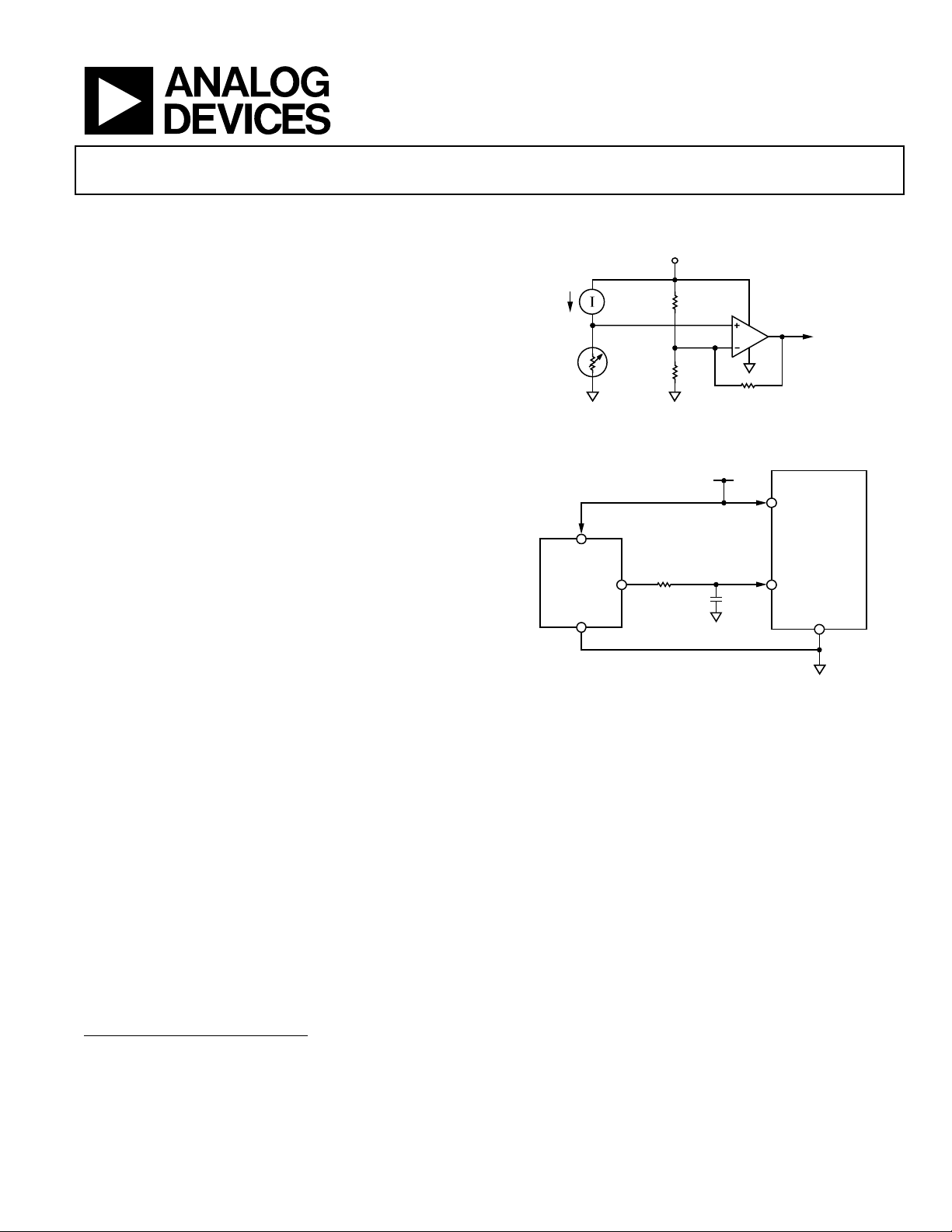
Figure 2. Application Ci rcuit
0.1µF
AD22100
V
OUT
00673-C-001
REFERENCE
ANALOG-TO-
DIGITAL
CONVERTER
INPUT
00673-C-002
The signal conditioning eliminates the need for any trimming,
buffering, or linearization circuitry, greatly simplifying the
system design and reducing the overall system cost.
The output voltage is proportional to the temperature x the
supply voltage (ratiometric). The output swings from 0.25 V at
−50°C to +4.75 V at +150°C using a single +5.0 V supply.
Due to its ratiometric nature, the AD22100 offers a costeffective solution when interfacing to an analog-to-digital
converter. This is accomplished by using the ADC’s +5 V
power supply as a reference to both the ADC and the AD22100
eliminating the need for and cost of a precision reference (see
Figure 2).
1
Protected by U.S. Patent No. 5,030,849 and 5,243,319.
Rev. D
Information furnished by Analog Devices is believed to be accurate and reliable.
However, no responsibility is assumed by Analog Devices for its use, nor for any
infringements of patents or other rights of third parties that may result from its use.
Specifications subject to change without notice. No license is granted by implication
or otherwise under any patent or patent rights of Analog Devices. Trademarks and
registered trademarks are the property of their respective owners.
One Technology Way, P.O. Box 9106, Norwood, MA 02062-9106, U.S.A.
Tel: 781.329.4700
Fax: 781.326.8703 © 2004 Analog Devices, Inc. All rights reserved.
www.analog.com

AD22100
TABLE OF CONTENTS
Specifications..................................................................................... 3
Output Stage Considerations.......................................................7
Chip Specifications....................................................................... 3
Absolute Maximum Ratings............................................................ 4
ESD Caution.................................................................................. 4
Pin Configurations and Function Descriptions ........................... 5
Typical Performance Characteristics ............................................. 6
Theory of Operation ........................................................................ 7
Absolute Accuracy and Nonlinearity Specifications ............... 7
REVISION HISTORY
7/04—Data Sheet Changed from Rev. C to Rev. D
Change to AD22100K Specifications............................................. 3
Updated Outline Dimensions....................................................... 10
Changes to Ordering Guide.......................................................... 11
6/04—Data Sheet Changed from Rev. B to Rev. C
Changes to Format ............................................................. Universal
Changes to Specifications................................................................ 3
Changes to Chip Specifications ...................................................... 3
Changes to Ratiometricity Considerations Section..................... 8
Changes to Ordering Guide.......................................................... 10
Updated Outline Dimensions....................................................... 10
Ratiometricity Considerations ....................................................8
Mounting Considerations............................................................8
Thermal Environment Effects .....................................................8
Microprocessor A/D Interface Issues .........................................9
Use with a Precision Reference as the Supply Voltage................9
Outline Dimensions ....................................................................... 10
Ordering Guide .......................................................................... 11
12/94—Data Sheet Changed from Rev. A to Rev. B
Rev. D | Page 2 of 12

AD22100
SPECIFICATIONS
TA = 25°C and V+ = 4 V to 6.5 V, unless otherwise noted.
Table 1.
AD22100K AD22100A AD22100S
Parameter Min Typ Max Min Typ Max Min Typ Max Unit
TRANSFER FUNCTION V
TEMPERATURE COEFFICIENT (V+/5 V) × 22.5 mV/°C
TOTAL ERROR
Initial Error
TA = 25°C ±0.5 ±2.0 ±1.0 ±2.0 ±1.0 ±2.0 °C
Error Overtemperature
TA = T
TA = T
MIN
MAX
±0.75 ±2.0 ±2.0 ±3.7 ±3.0 ±4.0 °C
±0.75 ±2.0 ±2.0 ±3.0 ±3.0 ±4.0 °C
Nonlinearity
TA = T
MAX
to T
MIN
0.5 0.5 1.0 % FS
OUTPUT CHARACTERISTICS
Nominal Output Voltage
V+ = 5.0 V, TA = 0°C 1.375 V
V+ = 5.0 V, TA = +100°C 3.625 V
V+ = 5.0 V, TA = −40°C 0.475 V
V+ = 5.0 V, TA = +85°C 3.288 V
V+ = 5.0 V, TA = −50°C 0.250 V
V+ = 5.0 V, TA = +150°C 4.750 V
POWER SUPPLY
Operating Voltage 4.0 5.0 6.5 4.0 5.0 6.5 4.0 5.0 6.5 V
Quiescent Current 500 650 500 650 500 650 µA
TEMPERATURE RANGE
Guaranteed Temperature Range 0 +100 −40 +85 −50 +150 °C
Operating Temperature Range −50 +150 −50 +150 −50 +150 °C
PACKAGE TO-92 TO-92 TO-92
SOIC SOIC SOIC
1
FS (full scale) is defined as the operating temperature range −50°C to +150°C. The listed maximum specification limit applies to the guaranteed temperature range.
For example, the AD22100K has a nonlinearity of (0.5%) × (200°C) = 1°C over the guaranteed temperature range of 0°C to +100°C.
CHIP SPECIFICATIONS
TA = 25°C and V+ = 5.0 V, unless otherwise noted.
Table 2.
Paramater Min Typ Max Unit
TRANSFER FUNCTION V
TEMPERATURE COEFFICIENT (V+/5 V) × 22.5 mV/°C
OUTPUT CHARACTERISTICS
Error
TA = 25°C ±0.5 ±2.0 °C
Nominal Output Voltage
TA = 25°C 1.938 V
POWER SUPPLY
Operating Voltage 4.0 5.0 6.5 V
Quiescent Current 500 650 µA
TEMPERATURE RANGE
Guaranteed Temperature Range +25 °C
Operating Temperature Range −50 +150 °C
= (V+/5 V) × [1.375 V +(22.5 mV/°C) × TA] V
OUT
1
= (V+/5 V) × [1.375 V +(22.5 mV/°C) × TA] V
OUT
Rev. D | Page 3 of 12

AD22100
ABSOLUTE MAXIMUM RATINGS
Table 3.
Parameter Rating
Supply Voltage 10 V
Reversed Continuous Supply Voltage −10 V
Operating Temperature –50°C to +150°C
Storage Temperature –65°C to +160°C
Output Short Circuit to V+ or Ground Indefinite
Lead Temperature Range
(Soldering 10 sec)
Junction Temperature 150°C
300°C
ESD CAUTION
ESD (electrostatic discharge) sensitive device. Electrostatic charges as high as 4000 V readily accumulate on
the human body and test equipment and can discharge without detection. Although this product features
proprietary ESD protection circuitry, permanent damage may occur on devices subjected to high energy
electrostatic discharges. Therefore, proper ESD precautions are recommended to avoid performance
degradation or loss of functionality.
Stresses above those listed under Absolute Maximum Ratings
may cause permanent damage to the device. This is a stress
rating only and functional operation of the device at these or
any other conditions above those indicated in the operational
section of this specification is not implied. Exposure to absolute
maximum rating conditions for extended periods may affect
device reliability.
Rev. D | Page 4 of 12

AD22100
PIN CONFIGURATIONS AND FUNCTION DESCRIPTIONS
V
O
V+
12 3
BOTTOM VIEW
(Not to Scale)
GND
00673-C-003
Figure 3. 3-Lead TO-92
Table 4. 3-Lead TO-92 Pin Function Descriptions
Pin No. Mnemonic Description
1 V+ Power Supply Input.
2 V
O
Device Output.
3 GND Ground Pin Must Be Connected to 0 V.
Table 5. 8-Lead SOIC Pin Function Descriptions
Pin No. Mnemonic Description
1 V+ Power Supply Input.
2 V
O
3 NC No Connect.
4 GND Ground Pin Must Be Connected to 0 V.
5 NC No Connect.
6 NC No Connect.
7 NC No Connect.
8 NC No Connect.
1
V+
AD22100
V
2
O
NC
3
TOP VIEW
(Not to Scale)
GND
4
NC = NO CONNECT
Figure 4. 8-Lead SOIC
Device Output.
8
NC
NC
7
NC
6
NC
5
00673-C-004
Rev. D | Page 5 of 12

AD22100
TYPICAL PERFORMANCE CHARACTERISTICS
16
14
12
T (T0-92)
10
(Sec)
τ
8
250
200
150
(°C/W)
JA
θ
(SOIC)
6
T (SOIC)
4
2
0
FLOW RATE (CFM)
Figure 5. Thermal Response vs. Flow Rate
100
(T0-92)
00673-C-005
800400
1200
50
FLOW RATE (CFM)
800400
12000
00673-C-006
Figure 6. Thermal Resistance vs. Flow Rate
Rev. D | Page 6 of 12

AD22100
V
THEORY OF OPERATION
The AD22100 is a ratiometric temperature sensor IC whose
output voltage is proportional to its power supply voltage. The
heart of the sensor is a proprietary temperature-dependent
resistor, similar to an RTD, which is built into the IC. Figure 7
shows a functional block diagram of the AD22100.
V+
V
OUT
R
T
00673-C-001
Figure 7. Simplified Block Diagram
The temperature-dependent resistor, labeled RT, exhibits a
change in resistance that is nearly linearly proportional to
temperature. This resistor is excited with a current source that is
proportional to the power supply voltage. The resulting voltage
across R
is therefore both supply voltage proportional and line-
T
arly varying with temperature. The remainder of the AD22100
consists of an op amp signal conditioning block that takes the
voltage across R
and applies the proper gain and offset to
T
achieve the following output voltage function:
= (V+/5 V) × (1.375 V + 22.5 mV/°C × TA)
V
OUT
OUTPUT STAGE CONSIDERATIONS
As previously stated, the AD22100 is a voltage output device. A
basic understanding of the nature of its output stage is useful for
proper application. Note that at the nominal supply voltage of
5.0 V, the output voltage extends from 0.25 V at –50°C to +4.75
V at +150°C. Furthermore, the AD22100 output pin is capable
of withstanding an indefinite short circuit to either ground or
the power supply. These characteristics are provided by the output stage structure shown in Figure 9.
4
3
2
1
0
ERROR (°C)
–1
–2
–3
–4
–50
TYPICAL ERROR
TEMPERATURE (°C)
Figure 8. Typical AD22100 Performance
+
MAXIMUM ERROR
OVER TEMPERATURE
MAXIMUM ERROR
OVER TEMPERATURE
100500
00673-C-007
150
ABSOLUTE ACCURACY AND NONLINEARITY SPECIFICATIONS
Figure 8 graphically depicts the guaranteed limits of accuracy
for the AD22100 and shows the performance of a typical part.
As the output is very linear, the major sources of error are offset, for instance error at room temperature, span error, and deviation from the theoretical 22.5 mV/°C. Demanding applications can achieve improved performance by calibrating these
offset and gain errors so that only the residual nonlinearity remains as a significant source of error.
V
OUT
00673-C-008
Figure 9. Output Stage Structure
The active portion of the output stage is a PNP transistor,
with its emitter connected to the V+ supply and its collector
connected to the output node. This PNP transistor sources the
required amount of output current. A limited pull-down capability is provided by a fixed current sink of about −80 µA, with
the term fixed referring to a current sink that is fairly insensitive
to either supply voltage or output loading conditions. The current sink capability is a function of temperature, increasing its
pull-down capability at lower temperatures.
Rev. D | Page 7 of 12

AD22100
Due to its limited current sinking ability, the AD22100 is incapable of driving loads to the V+ power supply and is instead
intended to drive grounded loads. A typical value for shortcircuit current limit is 7 mA, so devices can reliably source 1
mA or 2 mA. However, for best output voltage accuracy and
minimal internal self-heating, output current should be kept
below 1 mA. Loads connected to the V+ power supply should
be avoided as the current sinking capability of the AD22100 is
fairly limited. These considerations are typically not a problem
when driving a microcontroller analog-to-digital converter input
pin (see the Microprocessor A/D Interface Issues section).
RATIOMETRICITY CONSIDERATIONS
The AD22100 will operate with slightly better accuracy than
that listed in the data sheet specifications if the power supply is
held constant. This is because the AD22100’s output voltage
varies with both temperature and supply voltage, with some
errors. The ideal transfer function describing output voltage is:
(V+/5 V) × (1.375 V + 22.5 mV/°C × T
The ratiometricity error is defined as the percent change away
from the ideal transfer function as the power supply voltage
changes within the operating range of 4 V to 6.5 V. For the
AD22100, this error is typically less than 1%. A movement from
the ideal transfer function by 1% at 25°C, with a supply voltage
varying from 5.0 V to 5.50 V, results in a 1.94 mV change in
output voltage or 0.08°C error. This error term is greater at
higher temperatures because the output (and error term) is
directly proportional to temperature. At 150°C, the error in
output voltage is 4.75 mV or 0.19°C.
For example, with V
= 5.0 V, and TA = +25°C, the nominal
S
output of the AD22100 will be 1.9375 V. At V
nominal output will be 2.1313 V, an increase of 193.75 mV. A
proportionality error of 1% is applied to the 193.75 mV, yielding
an error term of 1.9375 mV. This error term translates to a
variation in output voltage of 2.1293 V to 2.3332 V. A 1.94 mV
error at the output is equivalent to about 0.08°C error in
accuracy.
If 150°C is substituted for 25°C in the above example, the error
term translates to a variation in output voltage of 5.2203 V to
5.2298 V. A 4.75 mV error at the output is equivalent to about
0.19°C error in accuracy.
)
A
= 5.50 V, the
S
MOUNTING CONSIDERATIONS
If the AD22100 is thermally attached and properly protected, it
can be used in any measuring situation where the maximum
range of temperatures encountered is between −50°C and
+150°C. Because plastic IC packaging technology is employed,
excessive mechanical stress must be avoided when fastening the
device with a clamp or screw-on heat tab. Thermally conductive
epoxy or glue is recommended for typical mounting conditions.
In wet or corrosive environments, an electrically isolated metal
or ceramic well should be used to shield the AD22100. Because
the part has a voltage output (as opposed to current), it offers
modest immunity to leakage errors, such as those caused by
condensation at low temperatures.
THERMAL ENVIRONMENT EFFECTS
The thermal environment in which the AD22100 is used
determines two performance traits: the effect of self-heating on
accuracy and the response time of the sensor to rapid changes
in temperature. In the first case, a rise in the IC junction
temperature above the ambient temperature is a function of two
variables: the power consumption of the AD22100 and the
thermal resistance between the chip and the ambient environment θ
the power dissipation by θ
vary widely for surroundings with different heat-sinking capacities, it is necessary to specify θ
6 shows how the magnitude of self-heating error varies relative
to the environment. A typical part will dissipate about 2.2 mW
at room temperature with a 5 V supply and negligible output
loading. Table 6 indicates a θ
heat sink, yielding a temperature rise of 0.4°C. Thermal rise will
be considerably less in either moving air or with direct physical
connection to a solid (or liquid) body.
Table 6. Thermal Resistance (TO-92)
Medium θJA (°C/W) t (sec)
Aluminum Block 60 2
Moving Air
Still Air
Self-heating error in °C can be derived by multiplying
JA.
. Because errors of this type can
JA
under several conditions. Table
JA
of 190°C/W in still air, without a
JA
2
Without Heat Sink 75 3.5
Without Heat Sink 190 15
1
Rev. D | Page 8 of 12

AD22100
Response of the AD22100 output to abrupt changes in ambient
temperature can be modeled by a single time constant t exponential function. Figure 10 shows the typical response time
plots for a few media of interest.
100
10
ALUMINUM
BLOCK
MOVING
AIR
STILL AIR
Figure 10. Response Time
TIME (sec)
00673-C-009
100
9080706050403020
% OF FINAL VALUES
90
80
70
60
50
40
30
20
10
0
0
The time constant t is dependent on θJA and the thermal capacities of the chip and the package. Table 6 lists the effective t (time
to reach 63.2% of the final value) for a few different media.
Copper printed circuit board connections were neglected in the
analysis; however, they will sink or conduct heat directly
through the AD22100’s solder plated copper leads. When faster
response is required, a thermally conductive grease or glue
between the AD22100 and the surface temperature being
measured should be used.
MICROPROCESSOR A/D INTERFACE ISSUES
The AD22100 is especially well suited to providing a low cost
temperature measurement capability for microprocessor/
microcontroller based systems. Many inexpensive 8-bit microprocessors now offer an onboard 8-bit ADC capability at a
modest cost premium. Total cost of ownership then becomes a
function of the voltage reference and analog signal conditioning
necessary to mate the analog sensor with the microprocessor
ADC. The AD22100 can provide an ideal low cost system by
eliminating the need for a precision voltage reference and any
additional active components. The ratiometric nature of the
AD22100 allows the microprocessor to use the same power
supply as its ADC reference. Variations of hundreds of millivolts in the supply voltage have little effect as both the
AD22100 and the ADC use the supply as their reference. The
nominal AD22100 signal range of 0.25 V to 4.75 V (−50°C to
+150°C) makes good use of the input range of a 0 V to 5 V
ADC. A single resistor and capacitor are recommended to provide immunity to the high speed charge dump glitches seen at
many microprocessor ADC inputs (see Figure 2).
An 8-bit ADC with a reference of 5 V will have a least significant bit (LSB) size of 5 V/256 = 19.5 mV. This corresponds to a
nominal resolution of about 0.87°C.
USE WITH A PRECISION REFERENCE AS THE SUPPLY VOLTAGE
While the ratiometric nature of the AD22100 allows for system
operation without a precision voltage reference, it can still be
used in such systems. Overall system requirements involving
other sensors or signal inputs may dictate the need for a fixed
precision ADC reference. The AD22100 can be converted to
absolute voltage operation by using a precision reference as the
supply voltage. For example, a 5.00 V reference can be used to
power the AD22100 directly. Supply current will typically be
500 µA, which is usually within the output capability of the
reference. Using a large number of AD22100s may require an
additional op amp buffer, as would scaling down a 10.00 V reference that might be found in instrumentation ADCs typically
operating from ±15 V supplies.
1
The time constant t is defined as the time to reach 63.2% of the final
temperature change.
2
1200 CFM.
Rev. D | Page 9 of 12

AD22100
Y
OUTLINE DIMENSIONS
0.210 (5.33)
0.170 (4.32)
0.205 (5.21)
0.175 (4.45)
0.135 (3.43)
MIN
0.050 (1.27)
MAX
0.500 (12.70) MIN
SEATING
PLANE
0.019 (0.482)
0.016 (0.407)
SQ
0.055 (1.40)
0.045 (1.15)
0.105 (2.66)
0.095 (2.42)
0.115 (2.92)
0.080 (2.03)
0.165 (4.19)
0.125 (3.18)
3
2
1
0.115 (2.92)
0.080 (2.03)
BOTTOM VIEW
CONTROLLING DIMENSIONS ARE IN INCHES; MILLIMETER DIMENSIONS
(IN PARENTHESES) ARE ROUNDED-OFF EQUIVALENTS FOR
REFERENCE ONLY AND ARE NOT APPROPRIATE FOR USE IN DESIGN
COMPLIANT TO JEDEC STANDARDS TO-226AA
Figure 11. 3-Pin Plastic Header Package [ TO-92]
(T-3)
Dimensions shown in inches and millimeters
5.00 (0.1968)
4.80 (0.1890)
4.00 (0.1574)
3.80 (0.1497)
0.25 (0.0098)
0.10 (0.0040)
COPLANARIT
0.10
CONTROLLING DIMENSIONS ARE IN MILLIMETERS; INCH DIMENSIONS
(IN PARENTHESES) ARE ROUNDED-OFF MILLIMETER EQUIVALENTS FOR
REFERENCE ONLY AND ARE NOT APPROPRIATE FOR USE IN DESIGN
85
1.27 (0.0500)
SEATING
PLANE
COMPLIANT TO JEDEC STANDARDS MS-012AA
Figure 12. 8-Lead Standard Small Outline Package [SOIC]
Dimensions shown in inches and millimeters
BSC
6.20 (0.2440)
5.80 (0.2284)
41
1.75 (0.0688)
1.35 (0.0532)
0.51 (0.0201)
0.31 (0.0122)
(R-8)
0.25 (0.0098)
0.17 (0.0067)
0.50 (0.0196)
0.25 (0.0099)
8°
1.27 (0.0500)
0°
0.40 (0.0157)
× 45°
Rev. D | Page 10 of 12

AD22100
ORDERING GUIDE
Models Temperature Range Package Description Package Outline
AD22100KT 0°C to +100°C 3-Pin Plastic Header Package (TO-92) T-3
AD22100KR 0°C to +100°C 8-Lead Standard Small Outline Package (SOIC) R-8
AD22100KR-REEL7 0°C to +100°C 8-Lead Standard Small Outline Package (SOIC) R-8
AD22100KRZ
AD22100KRZ-REEL71 0°C to +100°C 8-Lead Standard Small Outline Package (SOIC) R-8
AD22100AT –40°C to +85°C 3-Pin Plastic Header Package (TO-92) T-3
AD22100AR –40°C to +85°C 8-Lead Standard Small Outline Package (SOIC) R-8
AD22100AR-REEL –40°C to +85°C 8-Lead Standard Small Outline Package (SOIC) R-8
AD22100AR-REEL7 –40°C to +85°C 8-Lead Standard Small Outline Package (SOIC) R-8
AD22100ST –50°C to +150°C 3-Pin Plastic Header Package (TO-92) T-3
AD22100SR –50°C to +150°C 8-Lead Standard Small Outline Package (SOIC) R-8
AD22100SR-REEL7 –50°C to +150°C 8-Lead Standard Small Outline Package (SOIC) R-8
AD22100SRZ1 –50°C to +150°C 8-Lead Standard Small Outline Package (SOIC) R-8
AD22100SRZ-REEL71 –50°C to +150°C 8-Lead Standard Small Outline Package (SOIC) R-8
AD22100KCHIPS DIE
1
Z = Pb-free part.
1
0°C to +100°C 8-Lead Standard Small Outline Package (SOIC) R-8
Rev. D | Page 11 of 12

AD22100
NOTES
© 2004 Analog Devices, Inc. All rights reserved. Trademarks and registered trademarks are the property of their respective owners.
C00673–0–7/04(D)
Rev. D | Page 12 of 12
 Loading...