Analog Devices AD22050R-REEL, AD22050R, AD22050N Datasheet

AD22050
OUT
GND
IN+
IN–
+V
S
OFS A1
A2
A1
A2
Single-Supply Sensor
a
FEATURES
Gain of ⴛ20. Alterable from ⴛ1 to ⴛ160
Input CMR from Below Ground to 6ⴛ (V
Output Span 20 mV to (V
– 0.2) V
S
1-, 2-, 3-Pole Low-Pass Filtering Available
Accurate Midscale Offset Capability
Differential Input Resistance 400 k⍀
Drives 1 k⍀ Load to +4 V Using V
S
Supply Voltage: +3.0 V to +36 V
Transient Spike Protection and RFI Filters Included
Peak Input Voltage (40 ms): 60 V
Reversed Supply Protection: –34 V
Operating Temperature Range: –40ⴗC to +125ⴗC
APPLICATIONS
Current Sensing
Motor Control
Interface for Pressure Transducers, Position Indicators,
Strain Gages, and Other Low Level Signal Sources
= +5 V
– 1 V)
S
Interface Amplifier
AD22050
FUNCTIONAL BLOCK DIAGRAM
GENERAL DESCRIPTION
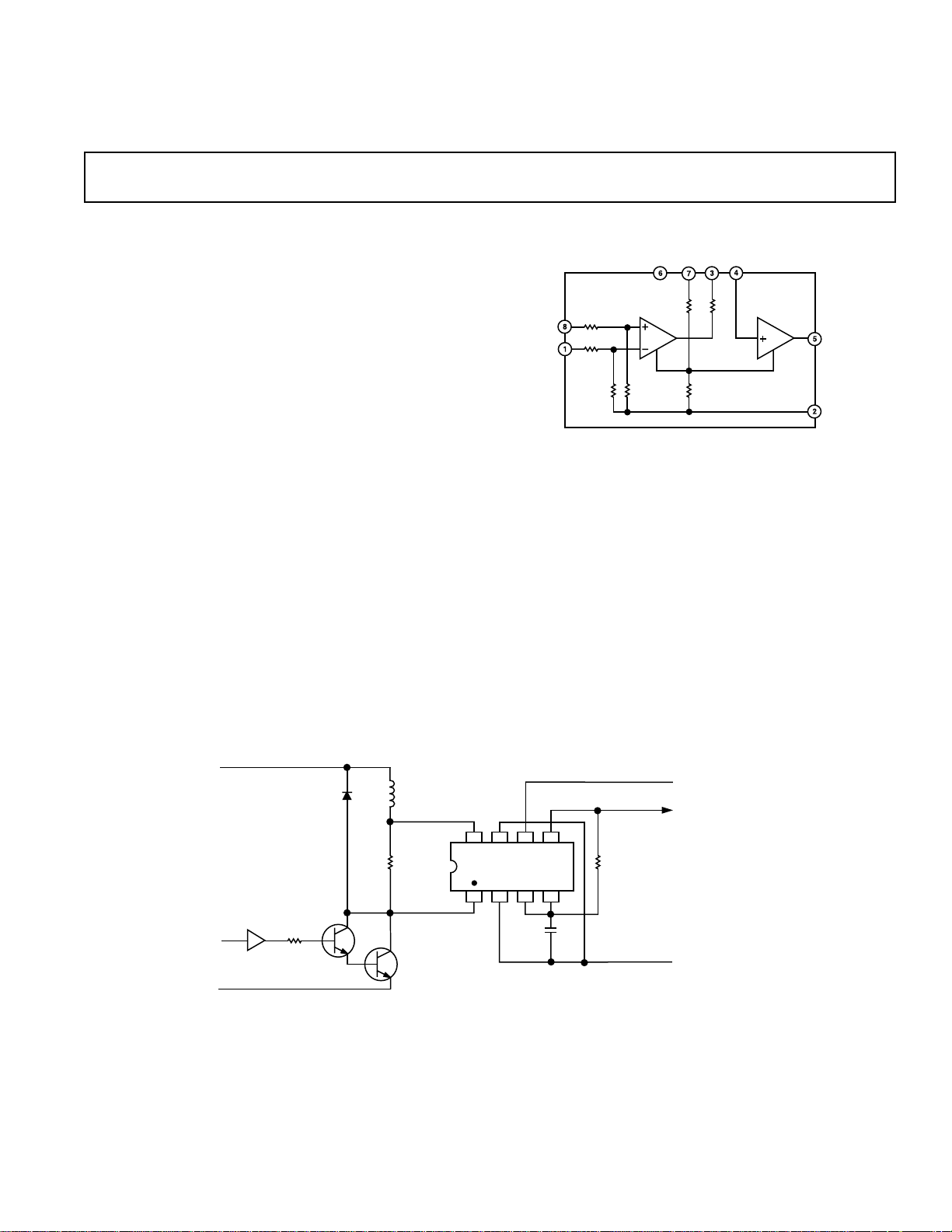
The AD22050 is a single-supply difference amplifier for amplifying and low-pass filtering small differential voltages (typically
100 mV FS at a gain of 40) from sources having a large commonmode voltage.
Supply voltages from +3.0 V to +36 V can be used. The input
common-mode range extends from below ground to +24 V using
+V
(CAR BATTERY)
S
CMOS DRIVER
CHASSIS
SOLENOID
LOAD
100mV
POWER
DARLINGTON
SINGLE-POLE LOW-PASS FILTERING, GAIN: 40
Figure 1. Typical Application Circuit for a Current Sensor Interface
a +5 V supply with excellent rejection of this common-mode
voltage. This is achieved by the use of a special resistive attenuator at the input, laser trimmed to a very high differential balance.
Provisions are included for optional low-pass filtering and gain
adjustment. An accurate midscale offset feature allows bipolar
signals to be amplified.
+5V
ANALOG OUTPUT
4V PER AMP
AD22050
C
200kV
CORNER FREQUENCY
= 0.796Hz-mF
ANALOG GROUND
REV. C
Information furnished by Analog Devices is believed to be accurate and
reliable. However, no responsibility is assumed by Analog Devices for its
use, nor for any infringements of patents or other rights of third parties
which may result from its use. No license is granted by implication or
otherwise under any patent or patent rights of Analog Devices.
One Technology Way, P.O. Box 9106, Norwood, MA 02062-9106, U.S.A.
Tel: 781/329-4700 World Wide Web Site: http://www.analog.com
Fax: 781/326-8703 © Analog Devices, Inc., 1999

AD22050–SPECIFICATIONS
(TA = +25ⴗC, VS = +5 V, and VCM = 0, RL = 10 k⍀ unless otherwise noted)
Parameter Test Conditions Min Typ Max Units
INPUTS (Pins 1 and 8)
+CMR Positive Common-Mode Range T
–CMR Negative Common-Mode Range T
CMRR
LF
CMRR
HF
R
INCM
R
MATCH
R
INDIFF
PREAMPLIFIER
G
CL
V
O
R
O
OUTPUT BUFFER
G
CL
V
O
R
O
OVERALL SYSTEM
G Gain
V
OS
Common-Mode Rejection Ratio f ≤ 10 Hz 80 90 dB
Common-Mode Rejection Ratio f = 10 kHz 60 75 dB
Common-Mode Input Resistances Pin 1 or Pin 8 to Pin 2 180 240 300 kΩ
Matching of Resistances ±0.5 %
Differential Input Resistance Pin 1 to Pin 8 280 400 kΩ
Closed-Loop Gain
Output Voltage Range (Pin 3) +0.01 +4.8 V
Output Resistance
Closed-Loop Gain
Output Voltage Range
1
2
1
3
Output Resistance (Pin 5) V
1
Over Temperature T
Input Offset Voltage
4
Over Temperature T
= T
A
= T
A
to T
MIN
MIN
MAX
to +85°C –1.0 V
+24 V
9.7 10.0 10.3
97 100 103 kΩ
R
≥ 10 kΩ 1.94 2.0 2.06
LOAD
TA = T
≥ 0.1 V dc, IO < 1 mA 2.0 Ω
O
V
≥ 0.1 V dc 19.9 20.0 20.1
O
= T
A
MIN
MIN
to T
to T
MAX
MAX
+0.02 +4.8 V
19.8 20.2
–1 0.03 1 mV
= T
A
MIN
to T
MAX
–3 3 mV
OFS Midscale Offset (Pin 7) Scaling 0.49 0.50 0.51 V/V
Input Resistance Pin 7 to Pin 2 2.5 3.0 kΩ
I
OSC
BW
–3 dB
SR Slew Rate 0.2 V/µs
N
SD
Short-Circuit Output Current TA = T
–3 dB Bandwidth VO = +1 V dc 30 kHz
Noise Spectral Density
3
f = 100 Hz to 10 kHz 0.2 µV/√Hz
MIN
to T
MAX
7 1125mA
POWER SUPPLY
V
S
I
S
Operating Range TA = T
Quiescent Supply Current
5
T
= +25°C, VS = +5 V 200 500 µA
A
MIN
to T
MAX
3.0 5 36 V
TEMPERATURE RANGE
T
OP
NOTES
1
Specified for default mode, i.e., with no external components. The overall gain is trimmed to 0.5%, while the individual gains of A1 and A2 may be subject to a
maximum ±3% tolerance. Note that the actual gain in a particular application can be modified by the use of external resistor networks.
2
The actual output resistance of A1 is only a few ohms, but access to this output, via Pin 3, is always through the resistor R12 (see Figure 16) which is 100 kΩ,
trimmed to ±3%.
3
For V
≤ 20 V. For V
CM
4
Referred to the input (Pins 1 and 8).
5
With VDM = 0 V. Differential mode signals are referred to as VDM, while VCM refers to common-mode voltages—see the section Product Description and Figure 3.
All min and max specifications are guaranteed, although only those marked in boldface are tested on all production units at final test.
Specifications subject to change without notice.
> 20 V, V
CM
Operating Temperature Range –40 +125 °C
≅ 1 mV/V × V
OL
CM
.
ORDERING GUIDE
Model Temperature Range Package Descriptions Package Options
AD22050N –40°C to +125°C Plastic DIP N-8
AD22050R –40°C to +125°C Plastic SOIC SO-8
AD22050R-Reel –40°C to +125°C Tape and Reel SO-8*
*Quantities must be in increments of 2,500 pieces each.
REV. C–2–

AD22050
TOP VIEW
(Not to Scale)
8
7
6
5
1
2
3
4
–IN
GND
A1
A2
+IN
OFFSET
+V
S
OUT
AD22050
ABSOLUTE MAXIMUM RATINGS*
Supply Voltage . . . . . . . . . . . . . . . . . . . . . . . . +3.0 V to +36 V
Peak Input Voltage (40 ms) . . . . . . . . . . . . . . . . . . . . . . +60 V
(Pin 7 to Pin 2) . . . . . . . . . . . . . . . . . . . . . . . . . . . .+20 V
V
OFS
Reversed Supply Voltage Protection . . . . . . . . . . . . . . . –34 V
Operating Temperature . . . . . . . . . . . . . . . . –40°C to +125°C
Storage Temperature . . . . . . . . . . . . . . . . . . –65°C to +150°C
Output Short Circuit Duration . . . . . . . . . . . . . . . . Indefinite
Lead Temperature Range (Soldering 60 sec) . . . . . . . . +300°C
*Stresses above those listed under Absolute Maximum Ratings may cause perma-
nent damage to the device. This is a stress rating only; the functional operation of
the device at these or any other conditions above those indicated in the operational
sections of this specification is not implied. Exposure to absolute maximum rating
conditions for extended periods may affect device reliability.
Plastic Mini-DIP Package
1
–IN
GND
2
A1
3
4
PIN CONFIGURATIONS
(N-8)
8
+IN
AD22050
TOP VIEW
(Not to Scale)
OFFSET
7
+V
6
OUTA2
5
S
CAUTION
ESD (electrostatic discharge) sensitive device. Electrostatic charges as high as 4000 V readily
accumulate on the human body and test equipment and can discharge without detection.
Although the AD22050 features proprietary ESD protection circuitry, permanent damage may
occur on devices subjected to high energy electrostatic discharges. Therefore, proper ESD
precautions are recommended to avoid performance degradation or loss of functionality.
PRODUCT DESCRIPTION
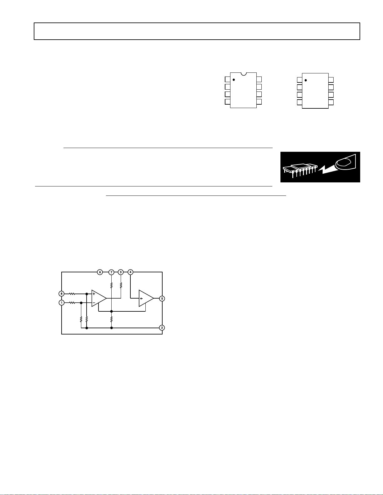
The AD22050 is a single-supply difference amplifier consisting
of a precision balanced attenuator, a very low drift preamplifier
and an output buffer amplifier (A1 and A2, respectively, in
Figure 2). It has been designed so that small differential signals (V
in the presence of large common-mode voltages (V
in Figure 3) can be accurately amplified and filtered
DM
) without
CM
the use of any other active components.
+V
S
OFS A1
A2
(Pin 6), permitting the conditioning and processing of bipolar
signals (see Strain Gage Interface section).
The output buffer A2 has a gain of ×2, setting the precalibrated,
overall gain of the AD22050, with no external components, to
×20. (This gain is easily user-configurable—see Altering the
Gain section for details.)
The dynamic properties of the AD22050 are optimized for
interfacing to transducers; in particular, current sensing shunt
resistors. Its rejection of large, high frequency, common-mode
signals makes it superior to that of many alternative approaches.
AD22050
This is due to the very careful design of the input attenuator and
the close integration of this highly balanced, high impedance
IN+
IN–
A1
A2
OUT
system with the preamplifier.
APPLICATIONS
The AD22050 can be used wherever a high gain, single-supply
differencing amplifier is required, and where a finite input resis-
GND
tance (240 kΩ to ground, 400 kΩ between differential inputs)
can be tolerated. In particular, the ability to handle a common-
Figure 2. Simplified Schematic
The resistive attenuator network is situated at the input to the
AD22050 (Pins 1 and 8), allowing the common-mode voltage at
Pins 1 and 8 to be six times greater than that which can be tolerated by the actual input to A1. As a result, the input common-
mode range extends to 6× (V
– 1 V).
S
Two small filter capacitors (not shown in Figure 2) have been
included at the inputs of A1 to minimize the effects of any spurious RF signals present in the signal.
Internal feedback around A1 sets the closed-loop gain of the
preamplifier to ×10 from the input pins; the output of A1 is
connected to Pin 3 via a 100 kΩ resistor, which is trimmed to
±3% (R12 in Figure 2) to facilitate the low-pass filtering of the
signal of interest (see Low-Pass Filtering section). The inclusion
of an additional resistive network allows the output of A1 to be
offset to an optional voltage of one half of that supplied to Pin 7;
in many cases this offset would be +V
REV. C
/2 by tying Pin 7 to +V
S
mode input considerably larger than the supply voltage is frequently of value.
Also, the output can run down to within 20 mV of ground,
provided it is not called on to sink any load current. Finally, the
output can be offset to half of a full-scale reference voltage (with
a tolerance of ±2%) to allow a bipolar input signal.
ALTERING THE GAIN
The gain of the preamplifier, from the attenuator input (Pins 1
and 8) to its output at Pin 3, is ×10 and that of the output
buffer, from Pin 4 to Pin 5, is ×2, thus making the overall default gain ×20. The overall gain is accurately trimmed (to within
±0.5%). In some cases, it may be desirable to provide for some
variation in the gain; for example, in absorbing the scaling error
of a transducer.
Figure 3 shows a general method for trimming the gain, either
upward or downward, by an amount dependent on the resistor,
R. The gain range, expressed as a percentage of the overall gain,
S
–3–
Plastic SOIC Package
(SO-8)
WARNING!
ESD SENSITIVE DEVICE
 Loading...