

SWITCH &
LIMITER
4
5
6
9
8
CHANNEL 1
CHANNEL 2
CHANNEL 3
2
1
20
3
7
11
10
13
12
CHANNEL 4
CHANNEL 5
14
15
16
17
19
18
CHIP
ENABLE
GND
+IN1
–IN1
–IN2
+IN2
–IN3
+IN3
–IN4
+IN4
–IN5
+IN5
POWER
OUT
OUT 1 & 2
OUT 3 & 4
OUT (3 × 4)
OUT 5
AD22001
IN
FUSE
1 & 2
IN
FUSE
5
+V
S
5-Channel Monolithic Comparator
FUSE
+V BATT
SWITCH
COPPER
SHUNT
RESISTOR
LAMP
SIGNAL CONDITIONING
AND SIGNAL PROCESSING
OUTPUT
a
FEATURES
Continuous Status Checks of Five Bulbs
Lamp Status Check in “ON” and “OFF” States
Status Checks of Two In-Line Fuses
Very Low Voltage Drop at Sensor Shunt Resistor
(Comparator Threshold 1.75 mV at 228C)
Temperature and Supply Voltage Compensated
Powered Directly from Car Battery: Protection
Included for Transient, Reverse Supply, Load Dump
Operating Temperature Range: –408C to +1258C
15 V CMOS Compatible Digital Output Signals
Voltage Limited Power Supply Output for 15 V CMOS
Logic ICs
GENERAL DESCRIPTION
The AD22001 is a monolithic, five-channel comparator circuit
for monitoring the functionality of lamps in automotive
applications.
The IC tests the series circuit leading to the lamp to determine
if the circuit is intact and a functional lamp is in the socket. The
AD22001 continuously checks the functionality of up to five
bulbs in either their “on” or “off” state, and also tests for the
presence of an in-line fuse in two of the series circuits.
Digital outputs indicate the status of each channel. Additionally,
the AD22001 provides a voltage limited power supply output to
supply 15 V CMOS circuits that may interface to the AD22001.
for Lamp Monitoring
AD22001*
FUNCTIONAL BLOCK DIAGRAM
REV. A
Information furnished by Analog Devices is believed to be accurate and
reliable. However, no responsibility is assumed by Analog Devices for its
use, nor for any infringements of patents or other rights of third parties
which may result from its use. No license is granted by implication or
otherwise under any patent or patent rights of Analog Devices.
Figure 1. Typical Application Circuit for a Single Channel Lamp Monitor
One Technology Way, P.O. Box 9106, Norwood, MA 02062-9106, U.S.A.
Tel: 617/329-4700 Fax: 617/326-8703

AD22001–SPECIFICA TIONS
(TA = +228C, VS = +13.5 V unless otherwise noted)
Parameter Test Conditions Min Typ Max Units
DIFFERENTIAL INPUTS (Voltage Drop from Shunt Resistor: Pins 4 & 5, 8 & 9, 10 & 11, 14 & 15, 16 & 17)
V
INDIFF
V
INCM
Comparator Threshold Voltage
Common-Mode Threshold Voltage
Power Supply Sensitivity of V
Temperature Compensation of V
I
I
INB
INC
Input Bias Current 10 µA
Constant Current Source
SINGLE-ENDED INPUTS (Fuse Monitoring: Pins 6, 19)
V
INF
Fuse Input Threshold Voltage
1
1
2
INDIFF
INDIFF
4
5
9 V ≤ VS ≤ 16 V 50 %
3
1.5 1.75 2.0 mV
5 V
3770 ppm/°C
30 60 µA
CHIP ENABLE CONTROL INPUT (Pin 1)
V
V
INCE
INCD
Chip Enable, Input High 9 V
Chip Disable (Stop Operation)
6
OUTPUTS (Pins 7, 12, 13, 18)
V
OUTL
Output Voltage, Low Load = 500 µA 0.6 V
Indicates No Fault in Lamp Circuit
V
OUTH
Output Voltage, High 9 V ≤ VS ≤ V
SSDH
V
–2.5 V
OUTPS
Indicates Fault in Lamp Circuit Load = 50 µA
POWER SUPPLY (Pin 2: +V
V
S
I
S
, Pin 20: GND)
S
Supply Voltage 930V
Quiescent Supply Current Pin 1 High 1 3 5 mA
V
: No Load Pin 1 Low 100 µA
OUTH
POWER SUPPLY OUTPUT (Pin 3)
V
OUTPS
I
OUTPS
Power Supply Output Voltage 10 V < VS < 14.5 V VS–0.5 VS–0.3 V
≤ 1 mA
I
Max Output Voltage 16 18 V
Power Supply Output Current
7
OUTPS
2mA
OPERATING SHUTDOWN (Safety Features)
V
V
SSDH
SSDL
Operation Shutdown at High 30 33 36 V
Power Supply Voltages
Operation Shutdown at Low 79V
Power Supply Voltage
8
9
4 V
6 V
OUTPS
S
V
V
TEMPERATURE RANGE
T
A
Operating Temperature Range –40 +125 °C
PACKAGE
Plastic DIP (N-20) AD22001N
NOTES
1
In the presence of a common-mode voltage greater than 5 V, if the shunt voltage applied to the comparator does not exceed the threshold (i.e., the bulb is switched
on but does not draw current), then the device will indicate a failure.
2
At VS = 13.5 V, the differential input threshold voltage is typically 1.75 mV. With an increase of VS, the threshold voltage, V
Power supply sensitivity of 50% means that when the power supply voltage VS increases by 10%, the threshold voltage V
centage value: 5%.
3
This is the temperature coefficient to compensate for any temperature influence on the external copper PCB track shunt resistors. 3770 ppm/°C is equal to 6.6 µV/°C.
4
This current source is used to test the lamp when it is switched off (cold lamp test).
5
If the voltage at the input from the fuse (Pin 6 or 19) does not exceed the threshold voltage, then the output will indicate a failure.
6
When the Chip Enable is open-circuited, the chip is disabled.
7
Shorting V
8
At this voltage, or above, the internal power supply and the power output V
9
Below the minimum voltage, the circuit will shut down. Above the maximum, the circuit will be on if enabled.
All min and max specifications are guaranteed, although only those marked in boldface are tested on all production units at final test.
Specifications subject to change without notice.
to ground will cause the device to stop operating for that period. However, the device will not suffer any damage.
OUTPS
will be shut off.
OUTPS
–2–
, will change as well.
INDIFF
will be increased by half of this per-
INDIFF
REV. A
SWITCH &
VOLTAGE LIMITER
INTERNAL
POWER SUPPLY
POWER
SUPPLY
OUTPUT
SIGNAL
OUT
GND
2
1
CAR
BATTERY
FUSE
SWITCH
COPPER
SHUNT
LIGHT
BULB
CE
–IN
+IN
NOTES
1. TEMPERATURE COMPENSATION FOR COPPER SHUNT RESISTOR
AND SUPPLY VOLTAGE COMPENSATION.
2. CURRENT SOURCE FOR COLD BULB CHECKING
(AVAILABLE IN CHANNELS 1, 2, 3 AND 4).
+V
S
V
INCE
V
INF
I
INB
V
INDIFF
I
INB
IN
FUSE
I
INC
ABSOLUTE MAXIMUM RATINGS*
Forward Supply Voltage . . . . . . . . . . . . . . . . . . . . . . . .+36 V
Reversed Supply Voltage . . . . . . . . . . . . . . . . . . . . . . . . –34 V
Forward Transient (40 ms) . . . . . . . . . . . . . . . . . . . . . . +60 V
Reverse Transient (40 ms) . . . . . . . . . . . . . . . . . . . . . . . –40 V
Voltage on Any Input Pin Relative to GND . . .–34 V to +36 V
Power Dissipation (V
= 13.5 V) . . . . . . . . . . . . . . . . 300 mW
S
Operating Temperature (Ambient) . . . . . . . –40°C to +125°C
Storage Temperature . . . . . . . . . . . . . . . . . . –65°C to +150°C
*Stresses above those listed under “Absolute Maximum Ratings” may cause
permanent damage to the device. This is a stress rating only, the functional
operation of the device at these or any other conditions above those indicated in the
operational sections of this specification is not implied. Exposure to absolute
maximum rating conditions for extended periods may affect device reliability.
ORDERING INFORMATION
Temperature Package
Model Range Option*
AD22001N –40°C to +125°C N-20
*N = Plastic DIP Package.
CONNECTION DIAGRAM
+V
POWER OUT
–IN 1
+IN 1
FUSE 1 + 2
OUT 1 + 2
+IN 2
–IN 2
+IN 3
CE
S
1
2
3
4
5
6
7
8
9
10
AD22001N
TOP VIEW
(Not to Scale)
20
GND
19
FUSE 5
18
OUT 5
17
+IN 5
16
–IN 5
15
+IN 4
14
–IN 4
13
OUT 3 + 4
12
OUT (3 × 4)
11
–IN 3
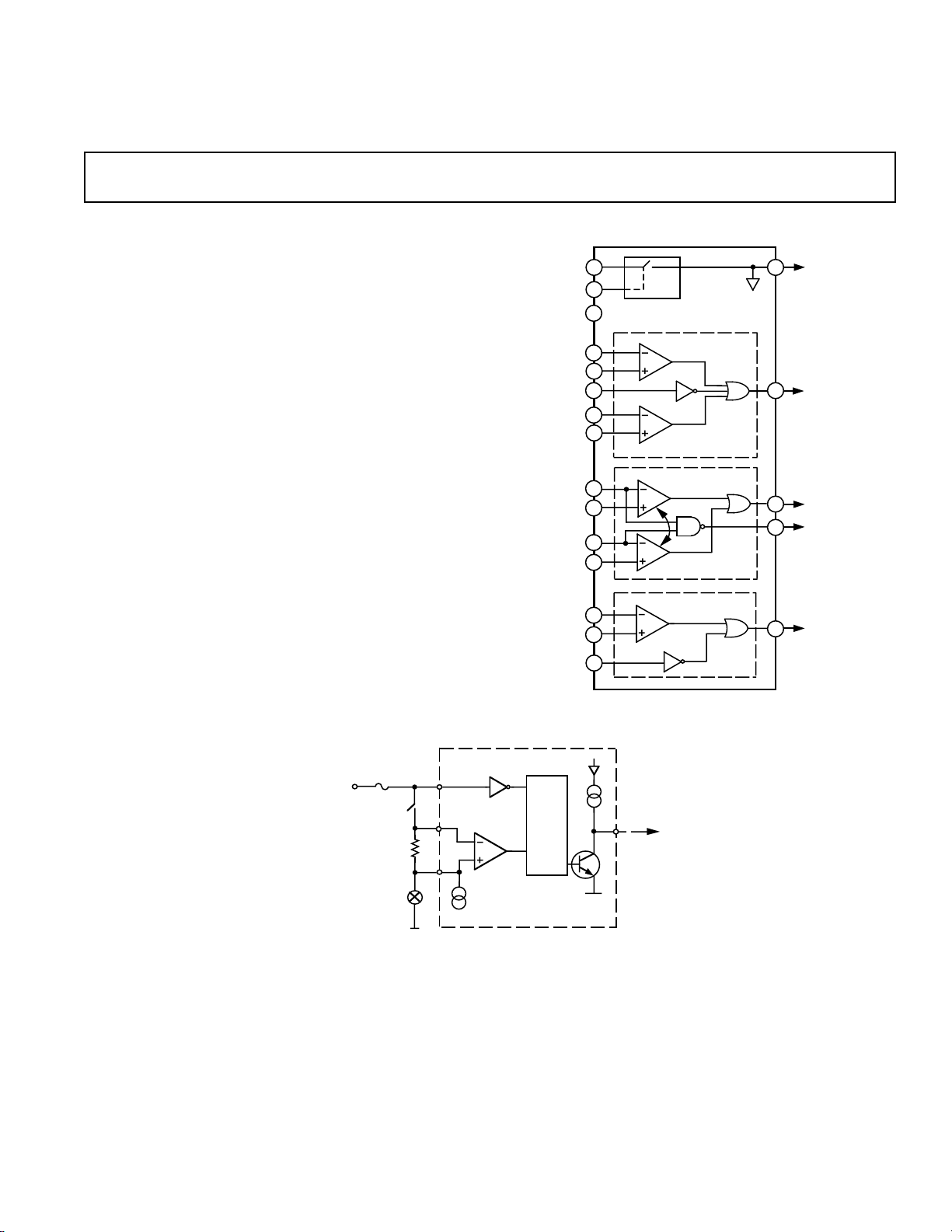
PRODUCT DESCRIPTION
The AD22001’s five comparators each monitor the voltage
across a current sensing shunt resistor which is part of a lamp
circuit. Each comparator has a small threshold voltage, nominally 1.75 mV. The output of the comparator will change state
as the voltage developed across the shunt (by the lamp current)
crosses the threshold level. Because the threshold voltage is very
small, copper tracks on the PC board can be used as shunt resistors with low power dissipation.
AD22001
Figure 2. Typical Block Diagram of One Channel and
Power Supply Control
The AD22001 has internal linear signal processing that compensates the comparator threshold voltage as the resistance of the
copper shunt resistor changes with varying temperature. The
comparator thresholds are also adjusted to compensate for
changes in lamp current due to power supply variations.
The AD22001 was designed for a common automotive lamp
monitoring application. The connection diagram (Figure 3) and
the application suggestion (Figure 4) show the different combinations of functions that are performed for each channel.
FUNCTIONAL DESCRIPTION
The AD22001 consists of fine sensitive comparators with
built-in offset plus biasing and support for comprehensive lamp
circuit monitoring. The comparators are arrayed as a single and
two groups of two (as shown in Figure 3) arranged to meet a
variety of requirements. Two or more AD22001s can be
combined. The comparators are basically similar with additional
features according to their place in the array.
Hot Lamp Test
Each comparator has a differential input with built-in threshold
of 1.75 mV, under nominal operating conditions. The comparators are intended to monitor the voltage developed across a low
resistance shunt by a lamp current. The comparators are active
whenever they are connected to the battery circuit. They indicate normal or okay (the series circuit to the lamp is intact)
when the threshold voltage of 1.75 mV is exceeded. This occurs
when the +input is driven negative with respect to the –input by
a voltage greater than the threshold. They also indicate normal
if they are not activated by common-mode battery voltage,
whether the threshold voltage is exceeded or not. They indicate
a fault if the common-mode is applied but the threshold is not
exceeded.
REV. A
–3–

AD22001
INPUTS AND SUPPLY OUTPUTS
POWER SUPPLY
+V
2
S
CHIP
GND
1 & 2
–IN2
+IN2
–IN3
+IN3
–IN4
+IN4
+IN5
FUSE
–IN1
+IN1
–IN5
1
20
4
5
6
9
8
11
10
14
15
16
17
19
5
ENABLE
R
S
IN
FUSE
R
S
R
S
R
S
R
S
IN
SWITCH &
LIMITER
CHANNEL 1
CHANNEL 2
CHANNEL 3
CHANNEL 4
CHANNEL 5
OUTPUT
3
V
SIGNAL OUTPUTS
OUT 1 & 2
7
13
OUT 3 & 4
12
OUT (3 × 4)
18
OUT 5
OUTPS
Figure 3. AD22001 Connection Diagram
Thus, in the absence of voltage applied to light the lamp, the
lamp resistance holds the common-mode voltage low, and no
fault is indicated. When the lamp circuit is powered, voltage on
the comparator inputs activates the comparator which indicates
a fault if the lamp current does not cause the shunt voltage to
exceed the threshold.
Cold Lamp Test
In addition to the standard hot lamp test, four of the comparators have a cold lamp test current of about 60 µA applied. If the
lamp circuit is not switched on but the lamp circuit is incomplete (failed lamp or connection), the small test current will
raise the common-mode voltage of the comparator at its input
and cause it to indicate a fault. Individual comparator inputs
draw about 10 µA each.
Description of Channel 5
The single comparator in Channel 5 is intended for brake-light
testing. Comparator 5 does not have the cold test feature, since
this lamp is normally tested in conjunction with the brake-light
switch. The comparator is combined with a fuse test circuit
which checks for battery voltage at its input. This input
normally connects between the fuse and brake-light switch.
The outputs of the hot lamp test and the fuse test are combined
at OUT 5 which indicates zero or low as the normal or okay
state and one or high if either test fails. The output will indicate
a fault if battery voltage is lost from the fuse test line, or if the
lamp circuit is powered, but the circuit fails to draw current.
Description of Channels 3 and 4
Comparators 3 and 4 are linked to test pairs of lamp circuits. In
addition to the hot lamp test, Channels 3 and 4 each have a cold
lamp test current. A fault for either test at input 3 or 4 will
cause their common output, OUT 3 & 4, to indicate failure
(registered as a one or high).
These comparators are intended for lamp circuits which are
switched simultaneously, but are fused independently. A special
linkage between the comparators causes them to indicate a fault
if common-mode voltage is applied to only one of the pair. This
functions as a test of both fuses.
One additional output is provided which tests when both lamps
are switched on (whether the lamp circuit draws current or not).
This circuit signals a zero or low level at OUT (3 3 4) whenever
both lamp circuits are powered (implying fuses are present) and
a one or high level otherwise.
Description of Channels 1 and 2
Comparators 1 and 2 are also linked and share a common output. A fault at either input will register as a one or high at OUT
1 & 2. Otherwise this output will be low. Each of these comparators also has a cold lamp test current. These comparators
are intended for two lamp circuits which have a common fuse,
and a fuse test line, similar to the brake-light test, is brought
out.
A summary of the tests performed by each channel is given in
Table I.
Signal Outputs
The signal outputs, OUT 1 & 2, OUT 3 & 4, OUT (3 3 4),
and OUT 5, are NPN collectors with pull-up currents provided
by the power control section. These currents are about 75 µA
each, and are intended to be sufficient to drive high level CMOS
inputs.
Table I. Summary of Recommended Applications and
Tests Performed for Each Channel
In a common automotive application, the AD22001 can be used
to monitor the following lamps:
Recommended Tests
Channel Applications Performed
1, 2 Fog Light Front I, II, III
Fog Light Rear
Number Plate Light
3, 4 Low Beam Headlight I, II, IV
Parking/Position
Taillight
5 Brake Light I, III
The following tests are performed and status indicated with the
AD22001:
Test Description
I Hot Lamp Test: Lamp is functional.
Test performed while lamp is switched on.
II Cold Lamp Test: Lamp is functional.
Test performed while lamp is switched off.
III Fuse is in place and functional.
IV The two monitored light bulbs are powered simulta-
neously. This can be used as an implicit fuse test.
–4–
REV. A

AD22001
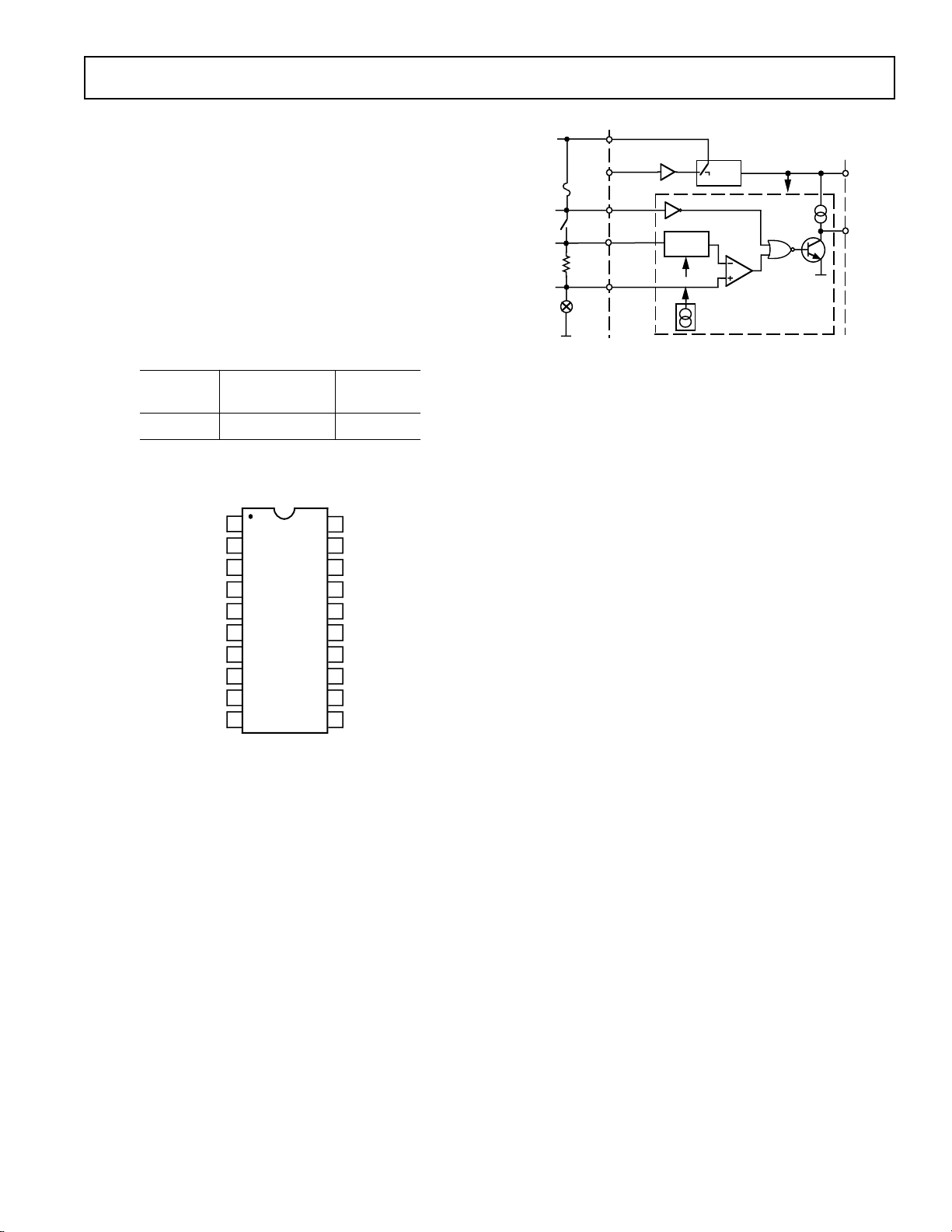
Threshold Biasing
The comparators are all activated by a common bias connection
which controls their threshold voltage. The threshold is
compensated for variations in temperature and operating
voltage. The temperature compensation is approximately +3770
ppm/°C. This causes the threshold to track the voltage across a
copper shunt operated at constant current and varying
temperature. The comparators are intended for use with small
value shunts made using normal copper tracks on PC cards.
+V
BATT
AD22001
CHIP ENABLE
1
+V
S
2
POWER
FUSE
OUT
LAMP
OUT 1 & 2
LAMP
LAMP
NOTE
R
ARE COPPER-TRACK SHUNT RESISTORS ON THE
S
PRINTED CIRCUIT BOARD.
FUSE
CHECK
R
3
4
R
S
5
6
7
8
S
9
10
R
S
GND
20
FUSE CHECK
19
18
17
16
15
14
13
12
11
R
R
OUT 5
S
S
OUT
3 & 4
OUT
(3 × 4)
LAMP
LAMP
FUSE
FUSE
FUSE
Figure 4. Application Suggestion
The power supply voltage compensation alters the comparator
threshold with a 50% sensitivity around the nominal 13.5 V
powering voltage. That is, a 10% change in battery voltage
results in a 5% change in threshold voltage. This compensation
approximately tracks the current in a hot lamp which typically
varies nonlinearly with applied voltage, with approximately 50%
sensitivity.
ON-OFF and Power Control
The AD22001 is intended to be powered directly from the
battery voltage. In normal operation an internal switch connects
internal circuits and the Power Out pin to the battery voltage,
under control of the Chip Enable. When Chip Enable is high
(above 9 V) the switch is on, the AD22001 is active and the
Power Out pin will be close to battery potential. When Chip
Enable is low, or open circuit, the switch will open and the
AD22001 will be inactive and Power Out will go low.
In order to protect the external circuits connected to Power Out
from overvoltage, the power switch is “soft” and limits the
output voltage to typically 16 V. If the applied voltage exceeds
this value, both Power Out and the internal voltage (from which
the threshold is derived) will limit. The limited Power Out
voltage will be available for moderate overvoltage conditions
such as double battery. If the applied voltage goes above
typically 33 V, the internal switch will be turned off, the lamp
monitor circuits will be inactivated and Power Out will go low
for the duration of the overvoltage.
Copper Resistors
Low value resistors can be produced as part of the printed
circuit pattern on copper clad boards. These resistors will have a
large positive TC, but this effect is compensated by the
temperature sensitive threshold in the AD22001.
At a design temperature of 24°C the sheet resistance, ρ
, of 35 µm
S
copper cladding is about 0.5 milliOhms per square (mΩ/sq),
and 70 µm copper is about 0.25 mΩ/sq. That is, a resistor made
from 35 µm copper with an aspect ratio (length/width) of 1 will
have a resistance of 0.5 mΩ, while with an aspect ratio of 4 its
resistance would be 2 mΩ, etc. The resistor can be designed for
a given value R by noting R = ρ
The sheet resistance ρ
is based on the thickness of copper
S
cladding (with 1 ounce per square foot (oz./ft
0.0014" approx. equal to 35 µm, and 2 oz./ft
L/W, so that L = RW/ρS.
S
2
) copper at
2
copper at 0.0028"
approx. equal to 70 µm) and the temperature. Choosing the
resistance value to correspond to the desired current trip level
and AD22001 threshold at 22°C, the 24°C “round number” is
convenient allowing a 2°C gradient from the resistor to the IC.
Choose W, the track width, as the larger of two values to be
determined. First the conductor should be sized so that the
nominal operating current results in only a small temperature
rise. This can be determined from the table from MIL STD275C, 9 Jan. 1970 (Figure 8).
Second, the width must be great enough to survive the peak
currents which are allowed by the fuse which supplies the track.
This can be determined from recommendations by the laminate
manufacturer, or the MIL table.
Using the larger of the two values determined for W, the length
of the resistor can be calculated. The resistor is defined by
“Kelvin” connections to the ends which sense the voltage across
this section of the track, and apply it to the differential input of
the AD22001 comparator.
As an example, consider the case of a parking lamp which
nominally draws 325 mA, and is on a circuit fused for 10A.
Suppose the board uses 70 µm (2 oz.) copper cladding, then a
conductor width of a few mils will suffice for the nominal
current. However, the 10A fuse may allow as much as 13.5A
current before it opens. A conductor 0.1" in width will carry
13.5A with less than 50°C rise in temperature, according to the
table.
Selecting 1/2 the nominal current as the AD22001 trip level
gives:
R = 1.75 mV/(325 mA/2)
or R = 10.769 mΩ.
Substituting these values in the expression for L,
L = 10.769 mΩ 3 0.1" /0.25 mΩ per sq
or L = 4.3".
A track of at least 0.1" in width should be used to convey this
current anywhere on the board. A section 4.3" long should be
sampled by Kelvin connections to the comparator differential
inputs.
This case, where the peak current available is large while the
sensed current is small, results in extremes of resistor length. In
such cases it may be convenient to bend or fold the shunt
REV. A
–5–

AD22001
resistance track. Bends in the track make the effective L/W more
difficult to calculate, however, certain common cases have been
evaluated.
To calculate the resistance of a track of width W with a 180°
bend at radius W/2 resulting in a spacing W, add a resistance
equivalent to 2.96 squares to account for the bend. Solving the
resistance equation for L/W,
L/W = R/ρ
= 10.769 mΩ/0.25 mΩ/sq,
S
or L/W = 43 squares.
Subtracting out the bend, the remainder is 40.04 squares.
Converting this to linear dimensions gives 4.004" at W = 0.1".
AD22001
(Not to Scale)
4
5
TO LAMP
2.002"
0.1"
0.05"0.1"
0.1"
2.002"
Figure 5. PCB Track Shunt Resistor with One 180° Bend
As shown in Figure 5, the contacts are made to the resistor
section of the track at 2.002" from the bend. The bend has a
uniform width of W, which is 0.1" in this case, and a radius of
W/2. As a result, the aspect ratio of the straight sections plus the
bend total 2.96 squares + (2.002" + 2.002")/0.1" or 43 squares.
The straight sections need not be of equal length, so long as
They have the proper total, and the shorter one is longer than
about 3W. A shorter resistor can be made by using more bends
and reducing the linear portion. For example, with three bends
the total length of four linear sections would be:
(43 squares – 3 3 2.96 squares/Bend)W
or (43 – 8.88) 3 0.1"= 3.412".
Assuming equal linear sections, the contacts and the bends
should be made at spacings of 3.412"/4 = 0.853", as shown in
Figure 6.
FROM SWITCH
TO LAMP
0.853"
0.05"0.1"
0.1"
0.1"
0.853"
AD22001
(Not to Scale)
4
5
Figure 6. PCB Track Shunt Resistor with Two 180° Bends
A 90° bend with an inside radius of W/2 and a smooth width of
W adds 0.341 squares to the aspect ratio as shown in Figure 7.
Note that the linear measurements are differently made at the
90° and the 180° bend.
Other styles of bend can be used with minor variation in total
resistance, however, we do not recommend the use of sharp
inside corners on high current conductors in general and shunt
resistors in particular. Sharp inside corners result in very high
local current density and poor resistance repeatability.
L1
W
W
2
W
L2
–6–
Figure 7. PCB Track Shunt Resistor with 90° Bend
REV. A

35.0
30.0
AD22001
100°C
25.0
20.0
15.0
12.0
10.0
8.0
7.0
CURRENT – Amperes
6.0
5.0
4.0
3.0
2.0
1.5
1.0
0.75
0.50
0.25
0.125
0
0
0.001
0.005
0.010
0.020
0.030
0.050
0.070
0.100
0.150
CONDUCTOR WIDTH – Inches
0.200
0.250
0.300
0.350
0.400
0 1 5 10 20 30 50 70 100 150 200 250 300 350 400 450 500 600 700
2
(1 oz/ft ) 0.0014"
2
(1/2 oz/ft ) 0.0007"
45°C
(2 oz/ft ) 0.0028"
CROSS SECTION – Mils
60°C
2
2
75°C
10°C
(3 oz/ft ) 0.0042"
30°C
20°C
2
Figure 8. Current-Carrying Capacities and Sizes of Etched Copper Conductors for Various Temperature Rises Above
Ambient (MIL-STD-275C, 9 January 1970)
REV. A
–7–

AD22001
0.210 (5.33)
MAX
0.200 (5.05)
0.125 (3.1)
OUTLINE DIMENSIONS
Dimensions shown in inches and (mm).
20-Pin Plastic DIP (N) Package
1.060 (26.92)
0.925 (23.50)
20
110
PIN 1
0.022 (0.558)
0.014 (0.356)
0.100
(2.54)
BSC
11
0.070 (1.77)
0.045 (1.15)
0.280 (7.11)
0.240 (6.10)
0.015 (0.38)
MIN
0.150
(3.81)
MIN
SEATING
PLANE
0.325 (8.25)
0.300 (7.62)
15°
0°
C1533–21–4/91
0.015 (0.381)
0.008 (0.203)
–8–
PRINTED IN U.S.A.
REV. A
 Loading...