


High Definition Audio SoundMAX® Codec
FEATURES
Ten 192 kHz DACs
Five independent stereo DAC pairs
7.1 surround sound plus independent headphone
Independent 8 kHz, 11.025 kHz, 16 kHz, 22.05 kHz, 32 kHz,
44.1 kHz, 48 kHz, 88.2 kHz, 96 kHz, 176.4 kHz, and 192 kHz
sample rates
Selectable stereo mixer on outputs
16-, 20-, and 24-bit PCM resolution
Six 192 kHz ADCs
Three independent stereo ADC pairs
Simultaneous record of up to three stereo channels
Support for quad microphone arrays plus independent
capture channel
Independent 8 kHz, 11.025 kHz, 16 kHz, 22.05 kHz, 32 kHz,
44.1 kHz, 48 kHz, 88.2 kHz, 96 kHz, 176.4 kHz, and 192 kHz
sample rates
16-, 20-, and 24-bit resolution
S/PDIF output
44.1 kHz, 48 kHz, 88.2 kHz, 96 kHz, 176.4 kHz, and 192 kHz
sample rates
16-, 20-, and 24-bit data widths
PCM, WMA/PRO, Dolby®, AC3, and DTS® formats
Digital PCM gain control
Digital PCM ADC/stream mixer
S/PDIF input
44.1 kHz, 48 kHz, 88.2 kHz, 96 kHz, 176.4 kHz, and 192 kHz
sample rates
16-, 20-, and 24-bit data widths
PCM, WMA/PRO, Dolby, AC3, and DTS formats
Digital PCM gain control
Auto synchronizes to source
High quality stereo CD input with GND sense
MONO_OUT pin for internal speakers or telephony
Retasking jack support
AD1988A/AD1988B
ENHANCED FEATURES
Three stereo headphone amps
AD1988A: Windows Vista™ Operating System Premium Logo
compliant
95 dB outputs
90 dB audio inputs
AD1988B: Windows Vista Premium Logo compliant and
Dolby Master Studio™ compliant
101 dB outputs
92 dB audio inputs
Internal 32-bit arithmetic for greater accuracy
Impedance and presence detection on all jacks
Analog PCBEEP and digital synthesis BEEP
C/LFE channel swap
Two general-purpose digital I/O (GPIO) pins
3.3 V analog and digital supplies
Reduced support components
Advanced power management modes
48-pin LQFP and LFCSP_VQ package options, Pb-free
Supports Andrea Active Noise Reduction headphones
Hardware volume control
Built-in microphone gain amps
Adjustable microphone bias pins
Rev. 0
Information furnished by Analog Devices is believed to be accurate and reliable. However, no
responsibility is assumed by Anal og Devices for its use, nor for any infringements of patents or ot her
rights of third parties that may result from its use. Specifications subject to change without notice. No
license is granted by implication or otherwise under any patent or patent rights of Analog Devices.
Trademarks and registered trademarks are the property of their respective owners.
One Technology Way, P.O. Box 9106, Norwood, MA 02062-9106, U.S.A.
Tel: 781.329.4700 www.analog.com
Fax: 781.461.3113 ©2006 Analog Devices, Inc. All rights reserved.

AD1988A/AD1988B
TABLE OF CONTENTS
Features.............................................................................................. 1
Pin Configuration and Function Descriptions..............................8
Enhanced Features............................................................................ 1
Revision History ............................................................................... 2
Functional Block Diagram .............................................................. 3
Specifications..................................................................................... 4
Test Conditions............................................................................. 4
Absolute Maximum Ratings............................................................ 7
Thermal Resistance ...................................................................... 7
ESD Caution.................................................................................. 7
REVISION HISTORY
10/06—Revision 0: Initial Version
Clarification of Output Configurations .................................. 11
HD Audio Widgets......................................................................... 12
Jack Presence Detection................................................................. 18
HD Audio Style Jack Presence Detection ............................... 18
Hardware Volume Control............................................................ 19
Outline Dimensions....................................................................... 20
Ordering Guide .......................................................................... 20
Rev. 0 | Page 2 of 20
AD1988A/AD1988B
R
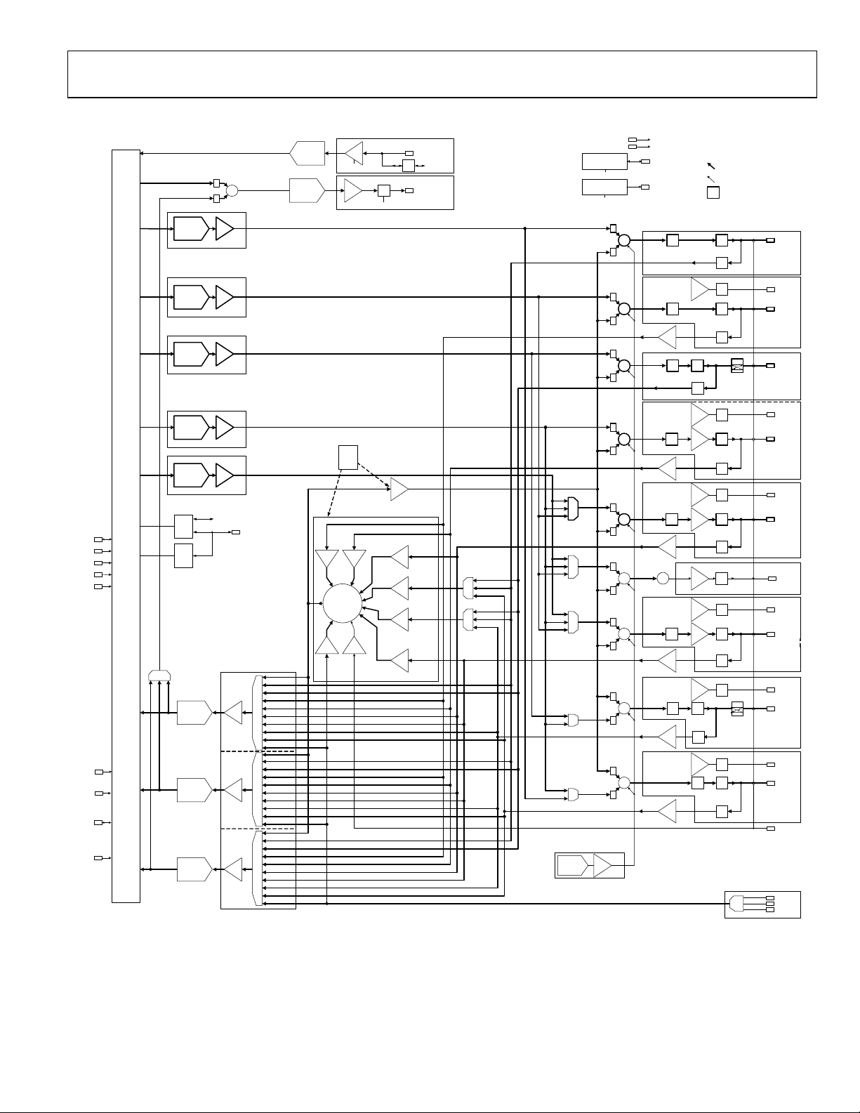
FUNCTIONAL BLOCK DIAGRAM
SYNC
ESET#
BITCLK
DVIO
DVDD
DVFILT
DVSS
NID:07
24 bit
32-192 kHz
PCM / Digital
S/PDIF RX
NID:1D
0(01)
M
Σ
1(0B)
M
DAC_ 4
24 bit
192 kHz
PCM
Σ∆ DAC
24 bit
192 kHz
PCM
Σ∆ DAC
24 bit
192 kHz
PCM
Σ∆ DAC
24 bit
H
D
A
U
D
192 kHz
PCM
Σ∆ DAC
24 bit
192 kHz
PCM
Σ∆ DAC
I
O
I
SDI
N
SDO
T
E
GPIO
Volume
Control
NID:1F
HW
Digital
A
-58.5 to0 dB
Digital
A
-58.5 to 0 dB
Digital
A
-58.5 to0 dB
Digital
A
-58.5 to0 dB
Digital
A
-58.5 to0 dB
GPIO _1
DAC_ 3
NID:06
DAC_ 2
NID:05
DAC_ 1
NID:04
DAC_ 0
NID:03
NID:0A
GPIO _0 /
Volume
NID:02
24 bit
32-192 kHz
PCM / Digital
S/PDIF TX
R
F
A
C
E
NID:0B
Selector
3:1
0(08)
2(0F)
+1.5V +/-10 %
(AD19 88L15 )
+3.3V +/-10 %
(AD19 88L33 )
+3.3V +/-10 %
+1.8V
1(09)
ADC_ 0
NID:08
24 bit
192 kHz
PCM
Σ∆ AD C
ADC_ 1
NID:09
24 bit
192 kHz
PCM
Σ∆ AD C
+5%
-20%
ADC_ 2
NID:0F
24 bit
192 kHz
PCM
Σ∆ AD C
ADCS E L_0
NID:0C
Digital/
Analog
GM
-58.5 to +2 2. 5dB
ADCS E L_1
NID:0D
Digital/
Analog
GM
-58.5 to +2 2. 5dB
ADCS E L_2
NID:0E
Digital/
Analog
GM
-58.5 to +2 2. 5dB
Sele cto r
10:1
Sele cto r
10:1
9(20-Mixer)
7(25–Port-H)
6(24–Port-G)
3 (3B – Port-F)
8(3D–Port-D)
Sele cto r
0(38–Port-A)
10:1
1(39–Port-B)
4(3C–Port-E)
2(3A–Port-C)
5(18-CD)
NID: 20
GAM
Digital
GAM
Input_En
-34. 5 to +12 dB
Digital
AM
-58.5 to0 dB
Mixer
Power
Control
NID:19
GAMGAM
3
5
2
1
Σ
4
0
7
6
GAM
7 (1A- PCBeep)
6(18 -CD)
Output_En
5(3B–Port-F)
-34.5to +12dB
NID:1C
ZGPIO_1
NID:1B
NID:21
AM
-46. 5 to 0 dB
3(3D–Port-D)
GAM
GAM
GAM
GAM
S/PDIF In / GPIO_1
S/PDIF OutZ
2(38–Port-A)
1(33–Port-C/H/G)
4(34–Port-E/H/G)
0(39–Port-B)
NID:33
NID:34
0(03)
1(04)
3:1
2(06)
NID:37
0(03)
1(04)
3:1
2(24)
1(25)
3:1
0(3A)
2(24)
1(25)
3:1
0(3C)
2(06)
NID:36
NID:30
0(03)
1(04)
3:1
2(06)
NID:32
0(05)
2:1
1(04)
NID:31
0(04)
2:1
1(0A)
Digital Beep AM
Figure 1. Block Diagram
MIC Bias R egulator
NID:35
Power
Control
VREF
NID:23
Power
Control
0(0A)
1(21)
0(06)
1(21)
0(05)
1(21)
0(04)
1(21)
0(37)
1(21)
0(36)
1(21)
0(30)
1(21)
1(21)
0(32)
1(21)
0(31)
NID:10
-45.0 to0dB
3dBSteps
AVSS
AVDD+3.3V+/-5%
MIC_BI AS_FILT
VREF_FI LT
NID:28
M
Σ
M
NID:2A
M
Σ
M
Boost
NID: 3B
NID:27
M
Σ
M
NID:29
M
Σ
M
Boost
NID: 3D
NID:22
M
Σ
M
Boost
NID: 38
NID:1E
M
M
M
NID:2D
Σ
Σ A
Stereo
Down-Mix
NID:2B
Σ
M
Boost
NID: 39
NID:26
M
Σ
M
Boost
NID: 3C
NID:2C
M
Σ
M
Boost
NID: 3A
MPORT-HZ
BIAS Z
MPORT-FZ
M
Z
EN
BIAS /
EAPD
HP
M
AMP
BIAS Z
HP
M
AMP
-46. 5 to 0 dB
BIAS Z
HP
M
AMP
BIAS Z
M Z
EN
BIAS /
EAPD
Stereo Paths
Mono Paths
101+ dB (AD1988B)
Split-Z
EN
EN
SWAP
Z
Z
EN
Z
EN
M
Z
EN
SWAP
Z
ZM
EN
CD
Diff
Amp
NID:25
NID:16
NID:24
NID:12
NID:11
NID:13
NID:14
NID:17
NID:15
NID:18
Surround
Center
PORT- F
MIC BIAS
Surround
Back
PORT- G
Center / LFE
PORT- D
MIC BIAS /
EAPD
PORT- D
HP-Front L/R
PORT- A
MIC BIAS
PORT- A
Headphone
MONO_OUT
PORT- B
MIC BIAS
PORT- B
Microphone
PORT- E
MIC BIAS
PORT- E
MIC 1/2
PORT- C
MIC BIAS /
EAPD
PORT- C
Line In
PCBeep
NID:1A
CD_L
CD_GND
CD_R
05843-011
Rev. 0 | Page 3 of 20

AD1988A/AD1988B
SPECIFICATIONS
TEST CONDITIONS
Test Conditions for the AD1988A and AD1988B are as follows, unless otherwise noted.
Analog Input/Output Conditions
Temperature at 25°C
Digital supply (DV
Analog supply (AV
) at 3.3 V ±10%
DD
) at 3.3 V ±5%
DD
MIC_BIAS_FILT at 5.0 V ±5%
Sample rate (F
) at 48 kHz
S
Input signal at 1008 Hz
Analog output pass band at 20 Hz to 20 kHz
DAC Conditions
Calibrated
Output −3 dB relative to full scale
10 kΩ output load: line out tests
32 Ω output load: headphone tests
ADC Conditions
Calibrated
0 db PGA gain
Input −3.0 dB relative to full scale
Table 1.
Typ
AD1988A/
Parameter Conditions/Comments Min
DIGITAL DECIMATION AND INTERPOLATION FILTERS
1
fS 8 kHz ~ 192 kHz
AD1988B
Max Unit
Pass Band 0 0.40 fSHz
Pass-Band Ripple ±0.005 dB
Stop Band 0.60 fS Hz
Stop Band Rejection −100 dB
Group Delay 20 1/fS
Group Delay Variation over Pass Band 0 µs
ANALOG-TO-DIGITAL CONVERTERS
Resolution
Gain Error Full-scale span relative to nominal input
1
24 Bits
±10 %
voltage
Interchannel Gain Mismatch Difference of gain errors ±0.2 ±0.5 dB
ADC Offset Error ±5 mV
ADC Crosstalk
Line Inputs Input L, Ground R, Read R;
1
−85 dB
Input R, Ground L, Read L
LINE_IN to Other −100 −80 dB
DIGITAL-TO-ANALOG CONVERTERS
Resolution
Gain Error Full-scale span relative to nominal input
1
24 Bits
±10 %
voltage
Interchannel Gain Mismatch Difference of gain errors ±0.2 ±0.5 dB
Tot al Out- of-Band Energ y
DAC Crosstalk
1
1
To 100 kHz −85 dB
Input L, Zero R, Read R;
−95 dB
Input R, Zero L, Read L
DAC VOLUMES—PROGRAMMABLE GAIN ATTENUATOR
Step Size DAC_0, DAC_1, DAC_2, DAC_3, DAC_4 +1.5 dB
Output Gain/Attenuation Range −58.5 0 dB
ADC VOLUMES—PROGRAMMABLE GAIN
AMPLIFIER/ATTENUATOR
Step Size ADCSEL_0, ADCSEL_1, ADCSEL_2 +1.5 dB
PGA Gain/Attenuation Range −58.5 +22.5 dB
ANALOG MIXER—PROGRAMMABLE GAIN
AMPLIFIER/ATTENUATOR
Signal-to-Noise Ratio (SNR)
1, 2
Input to output (including CD in) 95/96
Step Size All mixer inputs +1.5 dB
Input Gain/Attenuation Range All mixer inputs −34.5 +12.0 dB
Rev. 0 | Page 4 of 20

AD1988A/AD1988B
Typ
AD1988A/
Parameter Conditions/Comments Min
ANALOG LINE LEVEL OUTPUTS
Full-Scale Output Voltage Line out drive enabled 1.0 V rms
PORT-C, PORT-E, PORT-F, PORT-G, PORT-H, and
When ports are used as line level outputs 2.83 V p-p
MONO_OUT
Output Impedance
1
300 Ω
External Total Load Impedance 10 kΩ
Output Capacitance
External Load Capacitance
1
1
Total Harmonic Distortion (THD+N)
Dynamic Range
1
1
1000 pF
−85/−85 dB
−60 dB reference to fS A-weighted +95/+101 dB
ANALOG HP DRIVE OUTPUTS
Full-Scale Output Voltage Output drive enabled 1.0 V rms
PORT-A, PORT-B, and PORT-D When ports are used as outputs 2.83 V p-p
Output Impedance
External Load Impedance
Output Capacitance
External Load Capacitance
Total Harmonic Distortion (THD+N)
1
1
1
1
1
0.5 Ω
32 Ω
15 pF
1000 pF
10 kΩ load −83/−84 dB
32 Ω load −83/−84 dB
Dynamic Range
1
−60 dB reference to fS A-weighted, 10 kΩ or
32 Ω loads
ANALOG INPUTS When ports are used as inputs
PORT-G, PORT-H, or CD 1 V rms
2.83 V p-p
Microphone Boost Amplifiers
PORT-A, PORT-B, PORT-C, PORT-D, PORT-E, or PORT-F 0 dB boost 1 V rms
2.83 V p-p
+10 dB boost 0.316 V rms
0.894 V p-p
+20 dB boost 0.1 V rms
0.283 V p-p
+30 dB boost 0.032 V rms
0.089 V p-p
Input Impedance
1
PCBEEP 23 kΩ
PORT-G, PORT-H 60 kΩ
All others (with 0 dB boost) 150 kΩ
Input Capacitance
1
5 7.5 pF
ANALOG INPUT PERFORMANCE
Total Harmonic Distortion Plus Noise (THD+N)
1
−81/−82 dB
Dynamic Range −60 dB in reference to fS A-weighted +90/+92 dB
Signal-to-Noise Ratio (SNR)
2
+90/+92 dB
STATIC DIGITAL SPECIFICATIONS
Digital I/O (DVIO) DVIO @ 3.3 V ± 10% 2.97 3.3 3.63 V
VIH 2.0 V
VIL 0.8 V
VOH 2.4 V
VOL 0.6 V
AD1988B Max Unit
3
15 pF
3
+95/+101 dB
3
3
3
3
3
Rev. 0 | Page 5 of 20

AD1988A/AD1988B
Typ
AD1988A/
Parameter Conditions/Comments Min
POWER SUPPLY
Analog (AVDD) 3.3 V ± 5%
Power Supply Range 3.13 3.30 3.46 V
Power Dissipation 155/172 mW
Supply Current 47/52 mA
Digital (DVDD) 3.3 V ± 10%
Power Supply Range 2.97 3.30 3.63 V
Power Dissipation 247.5/238 mW
Supply Current 75/75 mA
Digital I/O (DVIO) 3.3 V ± 10%
Power Supply Range 2.97 3.30 3.63 V
Power Dissipation 3.96 mW
Supply Current 1.20 mA
Power Supply Rejection1 (AVDD) 100 mV p-p signal @ 1 kHz 80 dB V
1
Guaranteed, not tested.
2
SNR measurement defined as “the difference in level between a reference output signal and the device output with no signal applied.” This definition is taken from B.
Metzler, Audio Measurement Handbook, 1
3
RMS values assume sine wave input.
st
edition, Audio Precision, Inc., 1993, p. 165.
AD1988B Max Unit
Table 2. Power-Down States
AD1988A/AD1988B
Parameter Comments D-State DIDD Typ AIDD Typ Un it
POWER-DOWN STATES
FUNCTION Node D3 21/20 1.2/1.7 mA
DAC Pair Powered down saves (each) D3 6/6 5/5.6 mA
ADC Pair Powered down saves (each) D3 5.3/5.4 3.2/3.1 mA
Mixer Power Control (and Associated Amps) Saves D3 0/0 2.0/2.4 mA
MIC_BIAS Powered down saves D3 0/0 0.5/0.5 mA
RESET Low (active) state 2.9/2.7 3.1/3.4 mA
Rev. 0 | Page 6 of 20

AD1988A/AD1988B
ABSOLUTE MAXIMUM RATINGS
Table 3.
Parameter Rating
Digital (DVDD) −0.30 V to +3.65 V
Digital I/O (DVIO) −0.30 V to +3.65 V
Analog (AVDD) −0.30 V to +3.65 V
Input Current (Except Supply Pins) ±10.0 mA
Analog Input Voltage (Signal Pins) −0.30 V to AVDD + 0.3 V
Digital Input Voltage (Signal Pins) −0.30 V to DVIO + 0.3 V
Ambient Temperature (Operating) 0°C to +70°C
Storage Temperature Range −65°C to +150°C
Stresses above those listed under Absolute Maximum Ratings
may cause permanent damage to the device. This is a stress
rating only; functional operation of the device at these or any
other conditions above those indicated in the operational
section of this specification is not implied. Exposure to absolute
maximum rating conditions for extended periods may affect
device reliability.
THERMAL RESISTANCE
Ambient temperature ratings are as follows:
= T
T
AMB
− (PD × θCA)
CASE
where:
T
= case temperature in °C.
CASE
= power dissipation in W.
P
D
θ
= thermal resistance (case-to-ambient).
CA
Table 4. Thermal Resistance
Package Type θ
1
θ
JA
LQFP 48 17 31
LFCSP_VQ4 47 15 32
1
θJA = thermal resistance: junction-to-ambient.
2
θJC = thermal resistance: junction-to-case.
3
θCA = thermal resistance: case-to-ambient.
4
VQ = very thin quad.
2
θ
JC
3
Unit
CA
ºC/W
ºC/W
ESD CAUTION
Rev. 0 | Page 7 of 20

AD1988A/AD1988B
PIN CONFIGURATION AND FUNCTION DESCRIPTIONS
DV
GPIO_0/ VOLUM E
CORE
DV
DV
SDATA_OUT
BIT_CLK
DV
SDATA_IN
DV
SYNC
RESET
PCBEEP
S/PDIF-OUT
S/PDIF-IN/GPIO_1
PORT-H_R
4847464544434241403938
1
PIN 1
2
INDICATO R
3
I/O
4
SS
5
6
7
SS
8
9
DD
10
11
12
AD1988A/AD1988B
13141516171819
PORT-E_L
PORT-E_R
SENSE_A/SRC_B
SS
PORT-H_L
PORT-G_R
PORT-G_L
AV
TOP VIEW
(Not to Scale)
CD_L
CD_GND
PORT-F_L
PORT-F_R
Figure 2. LFCSP_VQ Pin Configuration
PORT-A_R
MONO_OUT
PORT-A_L
AVDDMIC_BIA S-A
2021222324
CD_R
PORT-B_L
PORT-C_L
PORT-B_R
37
PORT-C_R
PORT-D_R36
PORT-D_L
35
SENSE_B/SRC_A
34
MIC_BIAS_FILT
33
MIC_BIAS/EAPD-D
32
MIC_BIAS-E
31
MIC_BIAS-F
30
MIC_BIAS/EAPD-C
29
MIC_BIAS-B
28
VREF_FILT
27
AV
26
SS
AV
25
DD
TOP VIEW
(Not to Scale)
17
18
19
CD_L
PORT-F_L
PORT-F_R
SS
PORT-A_R40MONO_OUT39PORT-A_L38AV
41
20
CD_R
CD_GND
S/PDIF-OUT47S/PDIF-IN/GPIO _146PORT-H_R45PORT-H_L44PORT-G_R43PORT-G_L42AV
48
1
DV
GPIO_0/VOLUME
05843-001
CORE
DV
DV
SDATA_OUT
BIT_CLK
DV
SDATA_IN
DV
SYNC
RESET
PCBEEP
I/O
SS
SS
DD
PIN 1
2
3
4
5
6
7
8
9
10
11
12
AD1988A/AD1988B
13
14
15
16
PORT-E_L
PORT-E_R
SENSE_A/SRC_B
Figure 3. LFQP Pin Configuration
DD
MIC_BIAS-A
37
36
35
34
33
32
31
30
29
28
27
26
25
21
22
23
24
PORT-B_L
PORT-C_L
PORT-B_R
PORT-C_R
Table 5. Pin Function Descriptions
Pin
Mnemonic
DV
1 O
CORE
Number
GPIO_0/VOLUME 2 I/O
I/O Description
Filter Connection for Internal Core Voltage Regulator. This pin must be connected to filter
capacitors: 10 F, 1.0 F, and 0.1 F connected in parallel between Pin 1 and DV
SS
General-Purpose Input/Output Pin (Digital I/O). Digital signal used to control external circuitry.
(Pin 4 and Pin 7).
Volume Control. When enabled, it can be used as an external volume control
DVIO 3 I Link Digital I/O Voltage Reference. 3.3 V (±10%).
DVSS 4, 7 I Digital Supply Return (Ground).
SDATA_OUT 5 I
Link Serial Data Output (Digital Interface). AD1988 input stream. Clocked on both edges of the
BIT_CLK.
BIT_CLK 6 O Link Bit Clock (Digital Interface). 24.000 MHz serial data clock.
SDATA_IN 8 I/O
Link Serial Data Input (Digital Interface). AD1988 output stream. Clocked only on one edge of
BIT_CLK.
DVDD 9 I
Digital Supply Voltage 3.3 V ± 10%. This is regulated down to 1.9 V on Pin 1 to supply the internal
digital core internal to the AD1988.
SYNC 10 I Link Frame Sync (Digital Interface). 48 kHz frame sync plus SDI stream IDs.
RESET
11 I Link Reset (Digital Interface). AD1988 master hardware reset.
PCBEEP 12 I Monaural Input from System for PCBEEP. Line level input.
SENSE_A/SRC_B 13 I/O Jack Sense A to Jack Sense D Input/Sense B Drive.
PORT-E_L, PORT-E_R 14, 15 I/O Left and Right Rear Panel Stereo Mic In/C/LFE (Analog Input/Output).
Input: line level input, supports microphones with MIC_BIAS and boost amplifiers.
Output: line level output.
PORT-F_L, PORT-F_R 16, 17 I/O Left and Right Rear Panel Stereo Mic In/Surround Rear (Analog Input/Output).
Input: line level input, supports microphones with MIC_BIAS and boost amplifiers.
Output: line level output only.
CD_L, CD_R 18, 20 I CD Audio Left Channel, CD Audio Right Channel.
CD_GND 19 I CD Audio Analog Ground Reference (for Analog CD Input). Line level input only.
PORT-B_L, PORT-B_R 21, 22 I/O Front Panel Stereo Mic In/Front Panel Headphones. Analog input/output.
Input: line level input, supports microphones with MIC Bias and boost amplifiers.
Output: line level output, capable of driving headphone load and power.
PORT-D_R
PORT-D_L
SENSE_B/S RC_A
MIC_BIAS_F ILT
MIC_BIAS/ EAPD-D
MIC_BIAS- E
MIC_BIAS- F
MIC_BIAS/ EAPD-C
MIC_BIAS- B
VREF_FILT
AV
SS
AV
DD
05843-003
Rev. 0 | Page 8 of 20

AD1988A/AD1988B
Pin
Mnemonic
PORT-C_L, PORT-C_R 23, 24 I/O Rear Panel Line-In/Surround Back Output. Analog input/output.
Input: line level input, supports microphones with MIC Bias and boost amplifiers.
Output: line level output only.
AVDD 25, 38 I
AVSS 26, 42 I
VREF_FILT 27 O
MIC_BIAS-B 28 O Switchable Microphone Bias for PORT-B. Capable of:
High-Z, 0 V, 1.65 V, 3.78 V, and 3.95 V (with 5.0 V on Pin 33).
High-Z, 0 V, 1.65 V, 2.86 V, and 3.10 V (with 3.3 V on Pin 33).
MIC_BIAS-C 29 O Switchable Microphone Bias for PORT-C. This pin has the same function as MIC_BIAS-B.
MIC_BIAS-F 30 O Switchable Microphone Bias for PORT-F. This pin has the same function as MIC_BIAS-B.
MIC_BIAS-E 31 O Switchable Microphone Bias for PORT-E. This pin has the same function as MIC_BIAS-B.
MIC_BIAS-D 32 O Switchable Microphone Bias for PORT-D. This pin has the same function as MIC_BIAS-B.
MIC_BIAS_FILT 33 I
SENSE_B/SRC_A 34 I/O Jack Sense E to Jack Sense H Input/Sense A Drive.
PORT-D_L, PORT-D_R 35, 36 I/O Left and Right Rear Panel Headphone (Front Line Out)/Stereo MIC In. Analog input/output.
Input: line level input, supports microphones with MIC_BIAS and boost amplifiers.
Output: line level output, capable of driving headphone load and power.
MIC_BIAS-A 37 O Switchable Microphone Bias for PORT-A. This pin has the same function as MIC_BIAS-B.
PORT-A_L, PORT-A_R 39, 41 I/O Left and Right Front Panel Headphone Output/Stereo MIC In. Analog input/output.
Input: line level input, supports microphones with MIC_BIAS and boost amplifiers.
Output: line level output, capable of driving headphone load and power.
MONO_OUT 40 O Monaural Output to Internal Speaker or Telephony Subsystem. Line level output only.
PORT-G_L, PORT-G_R 43, 44 Left and Right Rear Panel C/LFE Output/Line Input.
Input: line level input.
Output: line level output.
PORT-H_L, PORT-H_R 45, 46 Left and Right Rear Panel Surround Center/Side Output/Line Input. Analog input/output.
Input: line level input.
Output: line level output.
S/PDIF_IN/GPIO_1 47 I/O
S/PDIF_OUT 48 O S/PDIF_OUT. Supports S/PDIF output.
Number I/O Description
Analog Supply Voltage. 3.3 V only. Caution: Do not apply 5.0 V to this pin. AV
well regulated and filtered because supply noise degrades audio performance.
Analog Supply Return (Ground). AV
under, or close to, the AD1988A/AD1988B.
Voltage Reference Filter. This pin must be connected to filter capacitors: 1.0 F and 0.1 F
connected in parallel between Pin 27 and AV
Filter for Microphone Bias Boost Circuitry. Connect this pin to 5.0 V via a low-pass filter. When
connected in this way, the AD1988A/AD1988B are each capable of providing 3.95 V as a
microphone bias to all of the MIC_BIAS pins. If 5 V is not available, connect this pin to 3.3 V (AV
via a low-pass filter. The AD1988A/AD1988B produce a MIC_BIAS voltage relative to the AV
supply (typically 3.1 V @ AV
S/PDIF_IN/GPIO Pin. S/PDIF_IN supports S/PDIF input. When enabled, GPIO_1 can be used as a
GPIO pin.
= 3.3 V).
DD
supplies should be
DD
should be connected to DVSS using a conductive trace
SS
(Pin 26).
SS
DD
DD
)
Rev. 0 | Page 9 of 20

AD1988A/AD1988B
Table 6. Pins Grouped by Function
Function Pin No. Mnemonic
Digital Interface 5 SDATA_OUT
6 BIT_CLK
8 SDATA_IN
10 SYNC
11
Digital Input/Output 48 S/PDIF_OUT
47 S/PDIF_IN/GPIO_1
2 GPIO_0/VOLUME
Jack Sense 13 SENSE_A/SRC_B
34 SENSE_B/SRC_A
Filter/Reference 1 DV
27 VREF_FILT
33 MIC_BIAS_FILT
Microphone Bias 28 MIC_BIAS-B
29 MIC_BIAS-C
30 MIC_BIAS-F
31 MIC_BIAS-E
32 MIC_BIAS-D
37 MIC_BIAS-A
Power and Ground 9 DVDD
3 DVIO
4, 7 DVSS
25, 38 AVDD
26, 42 AVSS
Analog Input/Output 12 PCBEEP
14 PORT-E_L
15 PORT-E_R
16 PORT-F_L
17 PORT-F_R
18 CD_L
20 CD_R
21 PORT-B_L
22 PORT-B_R
23 PORT-C_L
24 PORT-C_R
35 PORT-D_L
36 PORT-D_R
39 PORT-A_L
40 MONO_OUT
41 PORT-A_R
43 PORT-G_L
44 PORT-G_R
45 PORT-H_L
46 PORT-H_R
RESET
CORE
Rev. 0 | Page 10 of 20

AD1988A/AD1988B
CLARIFICATION OF OUTPUT CONFIGURATIONS
DAC, ADC, and port assignments are arbitrary; however, ports
are optimized for certain configurations. Use the guidelines in
Tabl e 7, Ta ble 8 , and Tabl e 9 when selecting ports for particular
functions. Note the following for each of these tables:
• HP is the output capable of driving headphone load and
power
• MIC is input that supports microphones with MIC Bias
and boost amplifiers
• LO is the line level output
• LI is the line level input
In desktop applications with discreet jacks (the default
configuration), assign the ports as listed in
Table 7. Discreet Jacks (Default Configuration)
Port Function HP MIC LO LI
PORT-A Front Panel Headphone x x x x
PORT-B Front Panel Microphone x x x x
PORT-C Rear Panel Line-In x x x
PORT-D
PORT-E Rear Panel Microphone x x x
PORT-F
PORT-G Rear Panel C/LFE x x
PORT-H
MONO_OUT
Rear Panel
Front/Headphone
Rear Panel Surround-Rear
(5.1)
Rear Panel SurroundCenter/Side (7.1)
Internal Mono Speaker
(use GPIO as EAPD)
Tabl e 7.
x x x x
x x x
x x
x
In desktop applications with shared input/5.1 jacks, assign the
ports as listed in
Tabl e 8.
Table 8. Shared Input/5.1 Jacks
Port Function HP MIC LO LI
PORT-A Front Panel Headphone x x x x
PORT-B Front Panel Microphone x x x x
PORT-C
PORT-D
PORT-E
MONO_OUT
Rear Panel LineIn/Surround-Rear (5.1)
Rear Panel
Front/Headphone
Rear Panel
Microphone/C/LFE
Internal Mono Speaker
(use GPIO as EAPD)
x x x
x x x x
x x x
x
In notebook applications, to support fully retasking jacks, assign
the ports as listed in
Tabl e 9.
Table 9.
Port Function HP MIC LO LI
PORT-A Headphone Jack x x x x
PORT-B Microphone Jack x x x x
PORT-D Line-In Jack x x x x
PORT-C
PORT-E/PORT-F
Internal Stereo
Speakers (use GPIO as
EAPD)
Internal Quad
Microphone Array
(Optional)
x x x
x x x
Rev. 0 | Page 11 of 20

AD1988A/AD1988B
HD AUDIO WIDGETS
Table 10.
Node
ID
00
01
02
03
04
05
06
07
08
09
0A
0B
0C
0D
0E
0F
10
11
12
13
14
15
16
17
18
19
1A
1B
1C
1D
1E
1F
20
21
22
23
24
25
26
27
28
29
2A
2B
2C
2D
2F
30
31
32
33
Name
ROOT
FUNCTION
S/PDIF DAC
DAC_0
DAC_1
DAC_2
DAC_3
S/PDIF ADC
ADC_0
ADC_1
DAC_4
S/PDIF Mix Selector
ADC Selector 0
ADC Selector 1
ADC Selector 2
ADC_2
Digital Beep
PORT-A
PORT-D
MONO_OUT
PORT-B
PORT-C
PORT-F
PORT-E
CD IN
Mixer Power-Down
Analog PCBEEP
S/PDIF Out
S/PDIF In
S/PDIF Mixer
MONO_OUT Mixer
Volume Knob
Analog Mixer
Mixer Output Attenuator
PORT-A Mixer
VREF Power-Down
PORT-G
PORT-H
PORT-E Mixer
PORT-G Mixer
PORT-H Mixer
PORT-D Mixer
PORT-F Mixer
PORT-B Mixer
PORT-C Mixer
Stereo Mix-Down
BIAS Power-Down
PORT-B Out Selector
PORT-C Out Selector
PORT-E Out Selector
PORT-C In Selector
Type Description
Root Device identification
Function Designates this device as an audio codec
Audio output S/PDIF digital stream output interface
Audio output Stereo headphone channel digital/audio converters
Audio output Stereo front channel digital/audio converters
Audio output Stereo C/LFE channel digital/audio converters
Audio output Stereo surround-back (5.1) channel digital/audio converters
Audio input S/PDIF digital stream input interface
Audio input Stereo record Channel 0 audio/digital converters
Audio input Stereo record Channel 1 audio/digital converters
Audio output Stereo surround-side (7.1) channel digital/audio converters
Audio selector Selects the ADC to drive the S/PDIF mixer
Audio selector Selects and amplifies/attenuates the input to ADC_0
Audio selector Selects and amplifies/attenuates the input to ADC_1
Audio selector Selects and amplifies/attenuates the input to ADC_2
Audio input Stereo record Channel 2 audio/digital converters
Beep generator Internal digital PCBEEP signal
Pin complex Front panel headphone jack
Pin complex Rear panel front speaker jack
Pin complex Monaural output pin (internal speakers or telephony system)
Pin complex Front panel microphone jack
Pin complex Rear panel line-in jack
Pin complex Rear panel surround-back (5.1) jack
Pin complex Rear panel microphone jack
Pin complex Analog CD input
Power widget Powers down the analog mixer and associated amps
Pin complex External analog PCBEEP signal input
Pin complex S/PDIF output pin
Pin complex S/PDIF input pin
Audio mixer Mixes the selected ADC with the digital stream to drive S/PDIF out
Audio mixer Selects the source that drives the MONO_OUT signal
Vendor defined Hardware volume knob
Audio mixer Mixes individual gain analog inputs
Audio selector Attenuates the mixer output to drive the port mixers
Audio mixer Mixes the DAC_0 and mixer output amps to drive PORT-A
Vendor defined Powers down the internal and external VREF circuitry
Pin complex Rear panel C/LFE jack
Pin complex Rear panel surround-side (7.1) jack
Audio mixer Mixes the PORT-E selected DAC and mixer output amps to drive PORT-E
Audio mixer Mixes the DAC_3 and mixer output amps to drive PORT-G
Audio mixer Mixes the DAC_4 and mixer output amps to drive PORT-H
Audio mixer Mixes the DAC_1 and mixer output amps to drive PORT-D
Audio mixer Mixes the DAC_2 and mixer output amps to drive PORT-F
Audio mixer Mixes the PORT-B selected DAC and mixer output amps to drive PORT-B
Audio mixer Mixes the PORT-C selected DAC and mixer output amps to drive PORT-C
Audio mixer Mixes the stereo L/R channels to drive MONO_OUT
Vendor defined Powers down the internal MIC_BIAS_FILT and all MIC_BIAS pins
Audio selector Selects DAC_0, DAC_1, and DAC_3 for PORT-B
Audio selector Selects DAC_2 and DAC_4 for PORT-C
Audio selector Selects DAC_2 and DAC_4 for PORT-E
Audio selector Selects from the PORT-C, PORT-G, and PORT-H inputs to the mixer input
Rev. 0 | Page 12 of 20

AD1988A/AD1988B
Node
ID
34
36
37
38
39
3A
3B
3C
3D
Table 11. AD1988A Device Root and Function Node Parameters
Node Vendor ID Revision ID
ID Name 0x00 0x02 0x04 0x05 0x08 0x11
00 ROOT 11D41988 00100400 00010001
01 FUNCTION 0002003C 00000001 00010C0C 40000002
1
Silicon revision number may change without prior notice. Number shown is current at the publication date of this document.
Name
PORT-E In Selector
MONO_OUT Selector
PORT-A Out Selector
PORT-A Boost
PORT-B Boost
PORT-C Boost
PORT-F Boost
PORT-E Boost
PORT-D Boost
Type Description
Audio selector Selects from the PORT-E, PORT-G, and PORT-H inputs to the mixer input
Audio selector Selects DAC_0, DAC_1, and DAC_3 for MONO_OUT
Audio selector Selects DAC_0, DAC_1, and DAC_3 for PORT-A
Audio selector Microphone boost amp for PORT-A
Audio selector Microphone boost amp for PORT-B
Audio selector Microphone boost amp for PORT-C
Audio selector Microphone boost amp for PORT-F
Audio selector Microphone boost amp for PORT-E
Audio selector Microphone boost amp for PORT-D
Audio
1
Sub Node
Count
Function
Group Type
Function Group
Capabilities
GPIO
Capabilities
Table 12. AD1988B Device Root and Function Node Parameters
Audio
Node Vendor ID Revision ID
1
Sub Node
Count
Function
Group Type
Function Group
Capabilities
GPIO
Capabilities
ID Name 0x00 0x02 0x04 0x05 0x08 0x11
00 ROOT 11D4198B 00100300 00010001
01 FUNCTION 0002003C 00000001 00010C0C 40000002
1
Silicon revision number may change without prior notice. Number shown is current at the publication date of this document.
Rev. 0 | Page 13 of 20

AD1988A/AD1988B
Table 13. Widget Parameters
Widg et
Node
ID
01
02
03
04
05
06
07
08
09
0A
0B
0C
0D
0E
0F
10
11
12
13
14
15
16
17
18
19
1A
1B
1C
1D
1E
1F
20
21
22
23
24
25
26
27
28
29
2A
2B
2C
2D
2F
30
31
Capabilities
Type ID
X 000004C0 000E07FF 00000001 80000000 00000009 00052727
0 00030311 000E07E0 00000005 00000001
0 00000405 000E07FF 00000001 00000000 00000009 00052727
0 00000405 000E07FF 00000001 00000000 00000009 00052727
0 00000405 000E07FF 00000001 00000000 00000009 00052727
0 00000405 000E07FF 00000001 00000000 00000009 00052727
1 00130391 000E07E0 00000005 00000001
1 00100501 000E07FF 00000001 00000001 00000009
1 00100501 000E07FF 00000001 00000001 00000009
0 00000405 000E07FF 00000001 00000000 00000009 00052727
3 00300301 00000003
3 0030010D 00000007 80053627
3 0030010D 00000007 80053627
3 0030010D 00000007 80053627
1 00100501 000E07FF 00000001 00000001 00000009
7 0070000C 00000000 800B0F0F
4 0040018D 0000373F 00000001 80000000
4 0040018D 0000373F 00000001 80000000
4 0040010C 00000010 00000001 80051F1F
4 0040018D 0000373F 00000001 80000000
4 0040018D 00003737 00000001 80000000
4 0040018D 00003737 00000001 80000000
4 0040098D 00003737 00000001 80000000
4 00400001 00000020 00000000
5 00500500 00000002 00000009
4 00400000 00000020 00000000
4 0040030D 00000010 00000001 80052727
4 0040020B 00000020 80051F17 00000000
2 00200303 80000000 00000002
2 00200103 80000000 00000002
6 00600080 00000000 000000BF
2 0020010B 80051F17 00000008
3 0030010D 00000001 80051F1F
2 00200103 80000000 00000002
F 00F00100 00000008
4 0040098D 00000037 00000001 80000000
4 0040018D 00000037 00000001 80000000
2 00200103 80000000 00000002
2 00200103 80000000 00000002
2 00200103 80000000 00000002
2 00200103 80000000 00000002
2 00200103 80000000 00000002
2 00200103 80000000 00000002
2 00200103 80000000 00000002
2 00200100 00000001
F 00F00100 00000006
3 00300101 00000003
3 00300101 00000002
09 0A 0B 0C 0D 0E 0F 12 13
PCM Size,
Rate
Stream
Formats
Pin
Capabilities
Input Amp
Capabilities
Con. List
Length
Power
States
Output
Amp
Capabilities
Vol ume
Knob
Capabilities
Rev. 0 | Page 14 of 20

AD1988A/AD1988B
Vol ume
Knob
Capabilities
Node
ID
32
33
34
36
37
38
39
3A
3B
3C
3D
Output
Widg et
Capabilities
Type ID
3 00300101 00000002
3 00300101 00000003
3 00300101 00000003
3 00300101 00000003
3 00300101 00000003
3 0030010D 00000001 00270300
3 0030010D 00000001 00270300
3 0030010D 00000001 00270300
3 0030010D 00000001 00270300
3 0030010D 00000001 00270300
3 0030010D 00000001 00270300
09 0A 0B 0C 0D 0E 0F 12 13
PCM Size,
Rate
Stream
Formats
Pin
Capabilities
Input Amp
Capabilities
Con. List
Length
Power
States
Amp
Capabilities
Rev. 0 | Page 15 of 20

AD1988A/AD1988B
Table 14. Connection List
Node
ID
02 0000001D 1 1D
03 0
04 0
05 0
06 0
07 0000001C 1 1C
08 0000000C 1 0C
09 0000000D 1 0D
0A 0
0B 000F0908 3 08 09 0F
0C 2418BC38 00203D25 7 38 1 3C 18 24 25 3D 20
0D 2418BC38 00203D25 7 38 1 3C 18 24 25 3D 20
0E 2418BC38 00203D25 7 38 1 3C 18 24 25 3D 20
0F 0000000E 1 0E
10 0
11 00000022 1 22
12 00000029 1 29
13 0000002D 1 2D
14 0000002B 1 2B
15 0000002C 1 2C
16 0000002A 1 2A
17 00000026 1 26
18 0
19 00002120 2 20 21
1A 0
1B 00000002 1 02
1C 0
1D 00000B01 2 01 0B
1E 00002136 2 36 21
1F 0
20 3D383339 1A183B34 8 39 33 38 3D 34 3B 18 1A
21 00000020 1 20
22 00002137 2 37 21
23 25249811 2120BD38 8 11 1 18 24 25 38 1 3D 20 21
24 00000027 1 27
25 00000028 1 28
26 00002132 2 32 21
27 00002105 2 05 21
28 0000210A 2 0A 21
29 00002104 2 04 21
2A 00002106 2 06 21
2B 00002130 2 30 21
2C 00002131 2 31 21
2D 0000001E 1 1E
2F 15141211 00001716 6 11 12 14 15 16 17
30 00060403 3 03 04 06
31 00000A04 2 04 0A
32 00000405 2 05 04
33 0024253A 3 3A 25 24
34 0024253C 3 3C 25 24
Connections 0 1 2 3 4 5 6 7
0 to 3 4 to 7 Length NID I NID I NID I NID I NID I NID I NID I NID
Rev. 0 | Page 16 of 20

AD1988A/AD1988B
Node
ID
36 00060403 3 03 04 06
37 00060403 3 03 04 06
38 00000011 1 11
39 00000014 1 14
3A 00000015 1 15
3B 00000016 1 16
3C 00000017 1 17
3D 00000012 1 12
Table 15. Default Configuration Bytes
MSB 31 29 27 23 19 15 8 7 3
LSB 30 28 24 20 16 12 8 4 0
Node Location Default Conn Misc Def
ID Value Connectivity Chassis Position Device Type Color JD Ovrrd Assn Seq
11 02214030 Jack External Front HP out
12 01014010 Jack External Rear Line out
13 9913011F Fixed Internal Special 3 Speaker ATAPI Unknown 1 1 F
14 02A19040 Jack External Front Mic in
15 01813021 Jack External Rear Line in
16 01011012 Jack External Rear Line out
17 01A19020 Jack External Rear Mic in
18 9933012E Fixed Internal Special 3 CD ATAPI Unknown 1 2 E
1A 99F301F0 Fixed Internal Special 3 Other ATAPI Unknown 1 F 0
1B 014511F0 Jack External Rear S/PDIF out Optical Black 1 F 0
1C 01C511F0 Jack External Rear S/PDIF in Optical Black 1 F 0
24 01016011 Jack External Rear Line out
25 01012014 Jack External Rear Line out
1
Default configuration values are set on codec power-up only. To preserve modifications by BIOS control, default configuration values do not change by reset
operations.
Connections 0 1 2 3 4 5 6 7
0 to 3 4 to 7 Length NID I NID I NID I NID I NID I NID I NID I NID
1
⅛” jack
⅛” jack
⅛” jack
⅛” jack
⅛” jack
⅛” jack
⅛” jack
⅛” jack
Green 0 3 0
Green 0 1 0
Pink 0 4 0
Blue 0 2 1
Black 0 1 2
Pink 0 2 0
Orange 0 1 1
Gray 0 1 4
Rev. 0 | Page 17 of 20

AD1988A/AD1988B
JACK PRESENCE DETECTION
HD AUDIO STYLE JACK PRESENCE DETECTION
The AD1988 uses two jack sense pins for presence detection on
up to eight audio jacks. This, combined with the device identification engine, enables software to determine if there is a device
plugged into the circuit, and the type of device it is. Allowing
software to configure jacks and amplifiers, as necessary, ensures
proper audio operation.
Detect jack presence by using a resistor tree arrangement
detailed by the HD audio specification, allowing up to four
jacks per sense line. Jacks must have normally open, isolated
switches to use this method of jack presence detection.
For proper operation, there must be a 2.67 k 1% resistor
connected between SENSE_A and AV
1% resistor between SENSE_B and AV
, and another 2.67 k
DD
.
DD
The specific resistor values for each jack are listed in
Use 1% tolerance resistors to ensure accurate detection.
Table 16. Jack Sense Mapping
Resistor Value SENSE_A SENSE_B
(1% Tolerance) Name Port Node ID Name Port Node ID
2.67 kΩ Pull-up to AVDD Pull-up to AVDD
5.10 kΩ FRONT D 0x12 SURR_SIDE (7.1) H 0x25
10.0 kΩ LINE IN C 0x15 C/LFE G 0x24
20.0 kΩ FRONT_MIC B 0x14 SURR_BACK (5.1) F 0x16
39.2 kΩ HP_OUT A 0x11 REAR_MIC E 0x17
Tabl e 16 .
Rev. 0 | Page 18 of 20

AD1988A/AD1988B
V
HARDWARE VOLUME CONTROL
DD
R1
3.3kΩ
GPIO_0/ VOLUME
R2
10kΩ
SW1
UP
R3
5.1kΩ
SW2
DOWN
Figure 4 . Volume Control Circuitry
R4
3.3kΩ
OPTIONAL
SW3
MUTE
05843-008
The AD1988A/AD1988B support external volume control on
Pin 2 (GPIO_0/VOLUME). The circuit diagram in
Figure 4
allows up/down/mute control using only three switches and
four resistors external to the codec. The up/down switches can
also be replaced by a center-position-off SPDT toggle switch.
The mute switch is optional, but desirable, for a satisfactory user
interface.
To use the GPIO_0/VOLUME pin (Pin 2) as a GPIO pin, it is
recommended to pull it down using a 10 k resistor (Pin 2 to
DV
). In the GPIO configuration, the volume control widget
SS
has no effect.
When the GPIO_0/VOLUME pin (Pin 2) is used as a volume control, pull-up Pin 2 to AV
. The volume control widget operates
DD
the codec volumes only under software control. If one of the
buttons is pressed, the control volume setting is incremented
(up), decremented (down), or set Bit 7 (mute). The volume
control supports 40 steps (other than mute) and uses a range of
0 (0x00, minimum volume) to 63 (0x3F, maximum volume).
Pressing the mute switch (or both up and down simultaneously)
toggles Bit 7 which indicates mute on/off.
Rev. 0 | Page 19 of 20

AD1988A/AD1988B
OUTLINE DIMENSIONS
1.45
1.40
1.35
ROTATED 90° CCW
0.15
0.05
VIEW A
PIN 1
INDICATOR
SEATING
PLANE
0.75
0.60
0.45
0.20
0.09
7°
3.5°
0°
0.08 MAX
COPLANARITY
COMPLIANT TO JEDEC STANDARDS MS-026-BBC
1.60
MAX
VIEW A
1
12
0.50
BSC
LEAD PITCH
Figure 5. 48-Lead Low Profile Quad Flat Package [LQFP]
(ST-48)
Dimension shown in millimeters
7.00
BSC SQ
0.60 MAX
37
36
48
PIN 1
TOP VIEW
(PINS DOWN)
13
0.60 MAX
9.00
BSC SQ
0.30
0.23
0.18
37
24
0.27
0.22
0.17
36
25
48
BSC SQ
1
7.00
PIN 1
INDICATOR
1.00
0.85
0.80
12° MAX
SEATING
PLANE
TOP
VIEW
0.80 MAX
0.65 TYP
0.50 BSC
COMPLIANT TO JEDEC STANDARDS MO-220-VKKD-2
6.75
BSC SQ
0.20REF
0.50
0.40
0.30
0.05 MAX
0.02 NOM
COPLANARITY
0.08
25
24
EXPOSED
PAD
(BOTTOM VIEW)
5.50
REF
13
5.25
5.10 SQ
4.95
12
0.25 MIN
Figure 6. 48-Lead Lead Frame Chip Scale Package [LFCSP_VQ]
7 mm × 7 mm Body, Very Thin Quad
(CP-48-1)
Dimension shown in millimeters
ORDERING GUIDE
Model Audio Output Performance Temperature Range Package Description Package Option
AD1988AJSTZ
AD1988AJSTZ-RL
AD1988AJCPZ
AD1988AJCPZ-RL
AD1988BJSTZ
AD1988BJSTZ-RL
AD1988BJCPZ
AD1988BJCPZ-RL
1
Z = Pb-free part.
1
1
95 dB 0°C to 70°C 48-Lead LQFP, Reel ST-48
1
95 dB 0°C to 70°C 48-Lead LFCSP_VQ, Tray CP-48-1
1
95 dB 0°C to 70°C 48-Lead LFCSP_VQ, Reel CP-48-1
1
101 dB 0°C to 70°C 48-Lead LQFP, Tray ST-48
1
101 dB 0°C to 70°C 48-Lead LQFP, Reel ST-48
1
101 dB 0°C to 70°C 48-Lead LFCSP_VQ, Tray CP-48-1
1
101 dB 0°C to 70°C 48-Lead LFCSP_VQ, Reel CP-48-1
Dolby and Dolby Master Studio are trademarks of Dolby Laboratories. DTS is a trademark of DTS, Inc. Windows Vista is either a registered trademark or trademark of
Microsoft Corporation in the United States and/or other countries.
©2006 Analog Devices, Inc. All rights reserved. Trademarks and
registered trademarks are the property of their respective owners.
D05843-0-10/06(0)
95 dB 0°C to 70°C 48-Lead LQFP, Tray ST-48
Rev. 0 | Page 20 of 20
 Loading...