

R
AC ’97 SoundMAX® Codec
AC ’97 2.3 COMPATIBLE FEATURES
S/PDIF output, 20-bit data format, supporting
48 kHz and 44.1 kHz sample rates
Integrated stereo headphone amplifier
Variable sample rate audio
External audio power-down control
>90 dB dynamic range
Stereo full-duplex codec
20-bit PCM DAC
3 analog line-level stereo inputs for line-in, AUX, and CD
Mono line-level phone input
Dual MIC input with built-in programmable preamplifier
High quality CD input with ground sense
Mono output for speakerphone or internal speaker
power management support
48-lead LQFP package, Pb-free available
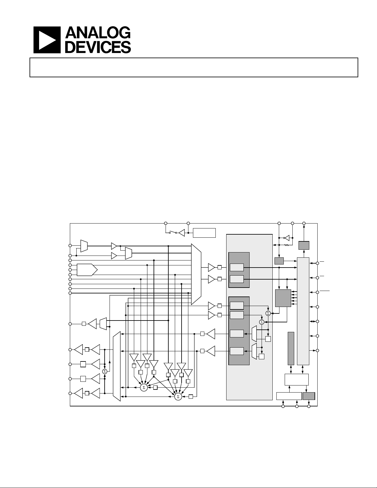
FUNCTIONAL BLOCK DIAGRAM
V
REFOUT
AD1981B
MIC1
MIC2
PHONE_IN
CD_L
CD_GND
CD_R
AUX_L
AUX_R
LINE_IN_L
LINE_IN_R
MONO_OUT
HP_OUT_L
LINE_OUT_L
LINE_OUT_
HP_OUT_R
MS
CD
DIFF AMP
M
HP
MZ
MZ
HP
M
M
MIC PREAMP
G
G
2CMIC
A
MIX
A
GA
MGAM
GA
MGAM
M
A
A
A
MGAM
OUTPUT SELECTOR
G
GA
MGAM
V
REF
GA
M
ENHANCED FEATURES
Stereo MIC preamplifier support
Built-in digital equalizer function for optimized
speaker sound
Full-duplex variable sample rates from 7040 Hz to
48 kHz with 1 Hz resolution
Jack sense pins for automatic output switching
Software-programmed V
microphone and external power amplifier
Split power supplies: 3.3 V digital and 5 V analog
Multiple codec configuration options
VOLTAGE
REFERENCE
CODEC CORE
PCM L/R
ADC RATE
M
M
M
M
16-BIT
Σ-∆ ADC
16-BIT
Σ-∆ ADC
16-BIT
Σ-∆ ADC
16-BIT
Σ-∆ ADC
20-BIT
Σ-∆ DAC
20-BIT
Σ-∆ DAC
PCM FRONT
DAC RATE
BYPASS
BYPASS
EQ
G
G
RECORD
SELECTOR
G
G
GA
M
GA
M
G = GAIN
A = ATTENUATION
M = MUTE
Z = HIGH Z
output for biasing
REFOUT
XTL_OUT XTL_IN SPDIF
PLL
ADC
AND
DAC
SLOT
LOGIC
EQ
EQ CORE STORAGE
AC '97
CONTROL
REGISTERS
ANALOG MIXING
CONTROL LOGIC
SPDIF
TX
AC '97 INTERFACE
AD1981B
ID0
ID1
RESET
SYNC
BIT_CLK
SDATA_OUT
SDATA_IN
EAPD
Rev. C
Information furnished by Analog Devices is believed to be accurate and reliable.
However, no responsibility is assumed by Analog Devices for its use, nor for any
infringements of patents or other rights of third parties that may result from its use.
Specifications subject to change without notice. No license is granted by implication
or otherwise under any patent or patent rights of Analog Devices. Trademarks and
registered trademarks are the property of their respective owners.
JS0 JS1 EAPD
03091-001
Figure 1.
One Technology Way, P.O. Box 9106, Norwood, MA 02062-9106, U.S.A.
Tel: 781.329.4700
Fax: 781.326.8703 © 2005 Analog Devices, Inc. All rights reserved.
www.analog.com

AD1981B
TABLE OF CONTENTS
Specifications..................................................................................... 3
PCM-Out Volume Register ....................................................... 18
Test Conditions............................................................................. 3
General Specifications ................................................................. 3
Power-Down States ...................................................................... 5
Timing Parameters....................................................................... 5
Absolute Maximum Ratings............................................................ 9
Environmental Conditions.......................................................... 9
Pin Configuration and Function Descriptions........................... 10
Indexed Control Registers............................................................. 12
Control Register Details ................................................................ 13
Reset Register.............................................................................. 13
Master Volume Register............................................................. 13
Headphone Volume Register .................................................... 14
Mono Volume Register .............................................................. 15
Phone Volume Register.............................................................. 15
MIC Volume Register................................................................. 16
Record Select Control Register................................................. 19
Record Gain Register................................................................. 19
General-Purpose Register ......................................................... 20
Power-Down Control/Status Register ..................................... 21
Extended Audio ID Register ..................................................... 22
Extended Audio Status and Control Register ......................... 22
PCM Front DAC Rate Register................................................. 23
PCM ADC Rate Register ........................................................... 23
SPDIF Control Register ............................................................. 24
EQ Control Register................................................................... 24
EQ Data Register........................................................................ 26
Mixer ADC, Input Gain Register ............................................. 26
Jack Sense/Audio Interrupt/Status Register............................ 27
Serial Configuration Register ................................................... 29
Miscellaneous Control Bit Register ......................................... 29
Line-In Volume Register............................................................ 16
CD Volume Register................................................................... 17
AUX Volume Register ................................................................ 17
REVISION HISTORY
1/05—Rev. B to Rev. C
Updated Format..................................................................Universal
Changes to Ordering Guide.......................................................... 32
6/03—Rev. A to Rev. B
Changes to TIMING PARAMETERS............................................ 4
Changes to ENVIRONMENTAL CONDITIONS ....................... 7
Changes to ORDERING GUIDE ................................................... 7
Updated OUTLINE DIMENSIONS ............................................ 27
Vendor ID Registers................................................................... 31
Outline Dimensions....................................................................... 32
Ordering Guide .......................................................................... 32
2/03—Rev. 0 to Rev. A
Changes to FUNCTIONAL BLOCK DIAGRAM.........................1
Changes to SPECIFICATIONS .......................................................2
Changes to TIMING PARAMETERS.............................................4
Change to Figure 6 Caption.............................................................6
................................................................................................................
10/02—Revision 0: Initial Version
Rev. C | Page 2 of 32

AD1981B
SPECIFICATIONS
TEST CONDITIONS
Standard test conditions, unless otherwise noted.
Table 1.
Parameter Test Condition
Temperature 25°C
Digital Supply (DVDD) 3.3 V
Analog Supply (AVDD) 5.0 V
Sample Rate (fS) 48 kHz
Input Signal 1008 Hz
Analog Output Pass Band 20 Hz to 20 kHz
DAC Calibrated
−3 dB Attenuation Relative to Full Scale
0 dB Input
10 kΩ Output Load (LINE_OUT)
32 Ω Output Load (HP_OUT)
ADC Calibrated
0 dB Gain
Input −3.0 dB Relative to Full Scale
GENERAL SPECIFICATIONS
Table 2.
Parameter Min Typ Max Unit
ANALOG INPUT
Input Voltage (RMS Values Assume Sine Wave Input)
LINE_IN, AUX, CD, PHONE_IN 1 V rms
2.83 V p-p
MIC_IN with 20 dB Gain 0.1 V rms
0.283 V p-p
MIC_IN with 0 dB Gain 1 V rms
2.83 V p-p
Input Impedance
Input Capacitance1 5 7.5 pF
MASTER VOLUME
Step Size (0 dB to −46.5 dB): LINE_OUT_L, LINE_OUT_R 1.5 dB
Output Attenuation Range1 46.5 dB
Step Size (0 dB to −46.5 dB): MONO_OUT 1.5 dB
Output Attenuation Range1 46.5 dB
Step Size (0 dB to −46.5 dB): HP_OUT_R, HP_OUT_L 1.5 dB
Output Attenuation Range Span1 46.5 dB
Mute Attenuation of 0 dB Fundamental1 80 dB
PROGRAMMABLE GAIN AMPLIFIER—ADC
Step Size (0 dB to 22.5 dB) 1.5 dB
PGA Gain Range 22.5 dB
ANALOG MIXER—INPUT GAIN/AMPLIFIERS/ATTENUATORS
Signal-to-Noise Ratio (SNR)
CD to LINE_OUT 90 dB
Other to LINE_OUT1 90 dB
1
20 kΩ
Rev. C | Page 3 of 32

AD1981B
Parameter Min Typ Max Unit
Step Size (+12 dB to −34.5 dB) (All Steps Tested):
MIC_IN, LINE_IN, CD, AUX, PHONE_IN, DAC 1.5 dB
Input Gain/Attenuation Range:
MIC_IN, LINE_IN, CD, AUX, PHONE_IN, DAC 46.5 dB
DIGITAL DECIMATION AND INTERPOLATION FILTERS1
Pass Band 0 0.4 × f
S
Pass-Band Ripple ±0.09 dB
Transition Band 0.4 × f
Stop Band 0.6 × f
S
S
0.6 × f
∞
S
Stop-Band Rejection −74 dB
Group Delay 16/fS s
Group Delay Variation over Pass Band 0 µs
ANALOG-TO-DIGITAL CONVERTERS
Resolution 16 Bits
Total Harmonic Distortion (THD) −84 dB
Dynamic Range (−60 dB Input THD + N Referenced to Full Scale, A-Weighted) 80 85 dB
Signal-to-Intermodulation Distortion1 (CCIF Method) 85 dB
ADC Crosstalk1
Line Inputs (Input L, Ground R, Read R; Input R, Ground L, Read L) −80 dB
Line_In to Other −100 −80 dB
Gain Error2 (Full-Scale Span Relative to Nominal Input Voltage) ±10 %
Interchannel Gain Mismatch (Difference of Gain Errors) ± 0.5 dB
ADC Offset Error1 ±5 mV
DIGITAL-TO-ANALOG CONVERTERS
Resolution 20 Bits
Total Harmonic Distortion (THD) LINE_OUT −85 dB
Total Harmonic Distortion (THD) HP_OUT −75 dB
Dynamic Range (−60 dB Input THD + N Referenced to Full Scale, A-Weighted) 85 90 dB
Signal-to-Intermodulation Distortion1 (CCIF Method) −100 dB
Gain Error2 (Output FS Voltage Relative to Nominal Output FS Voltage) ±10 %
Interchannel Gain Mismatch (Difference of Gain Errors) ±0.7 dB
DAC Crosstalk1 (Input L, Zero R, Measure R_OUT; Input R, Zero L, Measure
−80 dB
L_OUT)
Total Audible Out-of-Band Energy1 (Measured from 0.6 × fS to 20 kHz) −40 dB
ANALOG OUTPUT
Full-Scale Output Voltage; LINE_OUT and MONO_OUT 1 V rms
2.83 V p-p
Output Impedance1 800 Ω
External Load Impedance1 10 kΩ
Output Capacitance1 15 pF
External Load Capacitance1 100 pF
Full-Scale Output Voltage; HP_OUT (0 dB Gain) 1 V rms
External Load Impedance1 32 Ω
V
2.05 2.25 2.45 V
REF
V
(Programmable to 3.70 V Nominal) 2.25 V
REFOUT
V
Current Drive 5 mA
REFOUT
Mute Click (Muted Output Minus Unmuted Midscale DAC Output) ±5 mV
STATIC DIGITAL SPECIFICATIONS
High Level Input Voltage (VIH): Digital Inputs 0.65 × DVDD V
Low Level Input Voltage (VIL) 0.35 × DV
Hz
Hz
Hz
V
DD
Rev. C | Page 4 of 32

AD1981B
Parameter Min Typ Max Unit
High Level Output Voltage (VOH), IOH = 2 mA 0.9 × DVDD V
Low Level Output Voltage (VOL), IOL = 2 mA 0.1 × DV
Input Leakage Current −10 +10 µA
Output Leakage Current −10 +10 µA
POWER SUPPLY
Power Supply Range—Analog (AVDD) 4.5 5.5 V
Power Supply Range—Digital (DVDD) 3.0 3.47 V
Power Dissipation—5 V/3.3 V 400 mW
Analog Supply Current—5 V (AVDD) 50 mA
Digital Supply Current—3.3 V (DVDD) 46 mA
Power Supply Rejection (100 mV p-p Signal @ 1 kHz)1
40 dB
(At Both Analog and Digital Supply Pins, Both ADCs and DACs)
CLOCK SPECIFICATIONS1
Input Clock Frequency 24.576 MHz
Recommended Clock Duty Cycle 40 50 60 %
1
Guaranteed but not tested.
2
Measurements reflect main ADC.
V
DD
POWER-DOWN STATES
Values presented with V
Table 3.
Parameter Set Bits DVDD Typ AVDD Typ Unit
Fully Active No Bits Value 42 51 mA
ADC PR0 36 45 mA
DAC PR1 29 35 mA
ADC + DAC PR1, PR0 12 28 mA
Mixer PR2 42 24 mA
ADC + Mixer PR2, PR0 36 18 mA
DAC + Mixer PR2, PR1 29 9 mA
ADC + DAC + Mixer PR2, PR1, PR0 12 1.5 mA
Standby PR5, PR4, PR3, PR2, PR1, PR0 0 0 mA
Headphone Standby PR6 42 44 mA
REFOUT
not loaded.
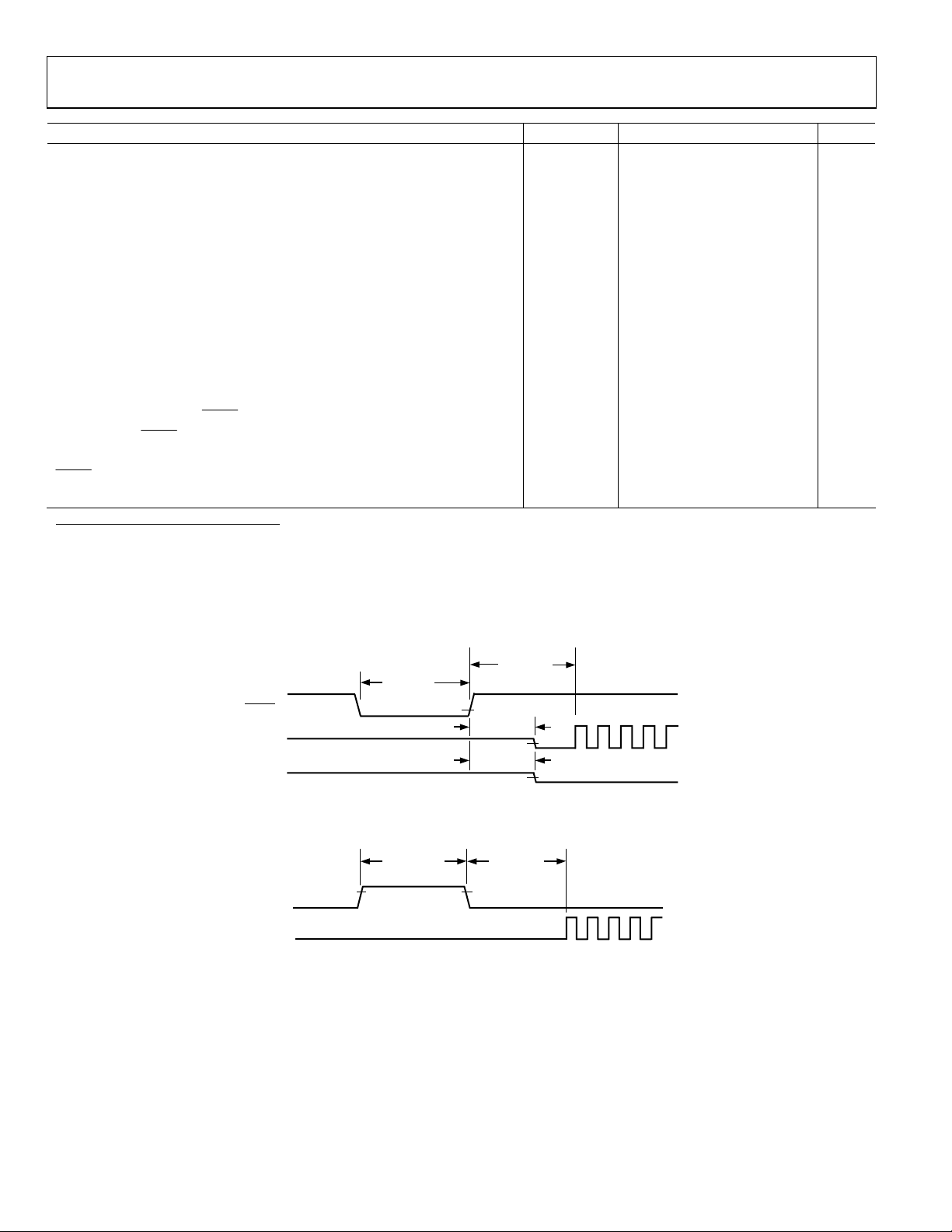
TIMING PARAMETERS
Guaranteed over operating temperature range.
Table 4.
Parameter Symbol Min Typ Max Unit
t
RESET Active Low Pulse Width
RESET Inactive to BIT_CLK Start-Up Delay
SYNC Active High Pulse Width t
SYNC Low Pulse Width t
SYNC Inactive to BIT_CLK Start-Up Delay t
BIT_CLK Frequency 12.288 MHz
BIT_CLK Frequency Accuracy ±1 ppm
BIT_CLK Period t
BIT_CLK Output Jitter
1, , 2 3
BIT_CLK High Pulse Width t
1.0 ms
RST_LOW
t
162.8 ns
RST2CLK
1.3 ms
SYNC_HIGH
19.5 µs
SYNC_LOW
162.8 ns
SYNC2CLK
CLK_PERIOD
81.4 ns
750 2000 ps
32.56 42 48.84 ns
CLK_HIGH
Rev. C | Page 5 of 32
AD1981B
Parameter Symbol Min Typ Max Unit
BIT_CLK Low Pulse Width t
SYNC Frequency 48.0 kHz
SYNC Period t
Setup to Falling Edge of BIT_CLK t
Hold from Falling Edge of BIT_CLK t
BIT_CLK Rise Time t
BIT_CLK Fall Time t
SYNC Rise Time t
SYNC Fall Time t
SDATA_IN Rise Time t
SDATA_IN Fall Time t
SDATA_OUT Rise Time t
SDATA_OUT Fall Time t
End of Slot 2 to BIT_CLK, SDATA_IN Low t
Setup to Trailing Edge of RESET (Applies to SYNC, SDATA_OUT)
Rising Edge of RESET to High Z Delay
Propagation Delay 15 ns
RESET Rise Time
Output Valid Delay from Rising Edge of BIT_CLK to SDI Valid 15 ns
1
Guaranteed but not tested.
2
Output jitter is directly dependent on crystal input jitter.
3
Maximum jitter specification for noncrystal operation only. Crystal operation maximum is much lower.
32.56 38 ns
CLK_LOW
SYNC_PERIOD
SETUP
HOLD
RISECLK
FALLCLK
RISESYNC
FALLSYNC
RISEDIN
FALLDIN
RISEDOUT
FALLDOUT
S2_PDOWN
t
SETUP2RST
t
OFF
20.8 ms
5 2.5 ns
5 ns
2 4 6 ns
2 4 6 ns
2 4 6 ns
2 4 6 ns
2 4 6 ns
2 4 6 ns
2 4 6 ns
2 4 6 ns
0 1.0 ms
15 ns
25 ns
50 ns
t
t
TRI2ACTV
t
TRI2ACTV
RST2CLK
03091-002
RESET
BIT_CLK
SDATA_IN
t
RST_LOW
Figure 2. Cold Reset Timing (Codec is Supplying the BIT_CLK Signal)
SYNC
BIT_CLK
t
SYNC_HIGH
Figure 3. Warm Reset Timing
t
SYNC2CLK
03091-003
Rev. C | Page 6 of 32
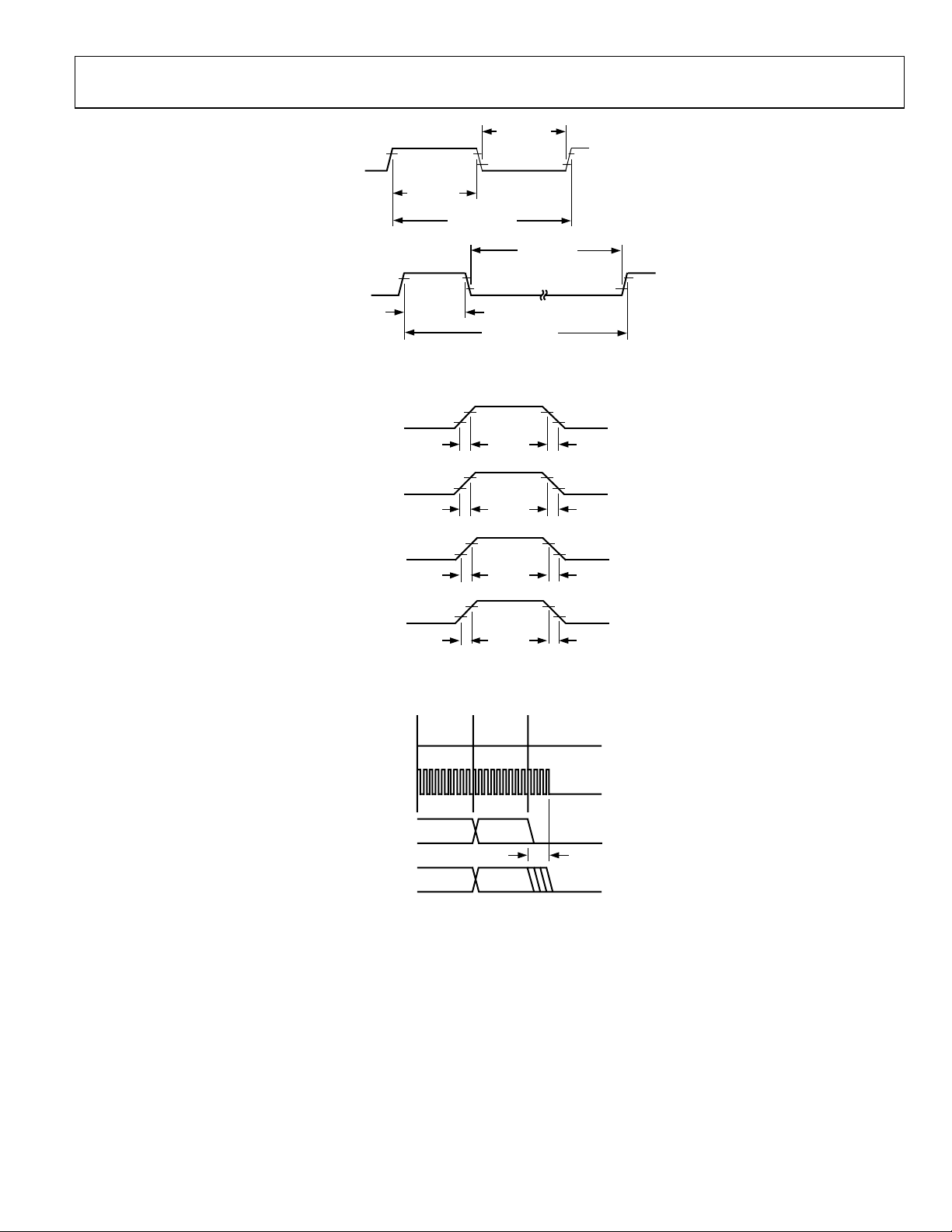
AD1981B
t
CLK_LOW
BIT_CLK
t
CLK_HIGH
t
CLK_PERIOD
t
SYNC_LOW
SYNC
t
SYNC_HIGH
t
SYNC_PERIOD
03091-004
Figure 4. Clock Timing
BIT_CLK
t
FALLCLK
t
FALLSYNC
t
FALLDIN
SYNC
SDATA_IN
t
RISECLK
t
RISESYNC
t
RISEDIN
SDATA_OUT
t
RISEDOUT
t
FALLDOUT
03091-005
Figure 5. Signal Rise and Fall Times
SLOT 1 SLOT 2
SYNC
BIT_CLK
SDATA_OUT
SDATA_IN
WRITE TO
BIT_CLK NOT TO SCALE
0x20
DATA
PR4
t
S2_PDOWN
03091-006
Figure 6. AC-Link Low Power Mode Timing
Rev. C | Page 7 of 32
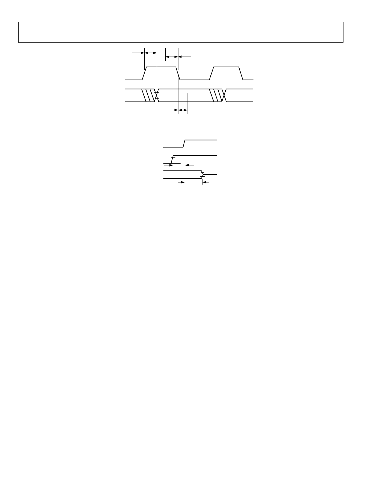
AD1981B
S
T
t
CO
t
SETUP
BIT_CLK
DATA_OU
SDATA_IN
SYNC
V
IH
V
OH
V
OL
t
HOLD
V
IL
03091-007
Figure 7. AC-Link Low Power Mode Timing, SYNC and BIT_CLK Chopped
RESET
SDATA_OUT
SDATA_IN, BIT_CLK,
EAPD, SPDIF_OUT
AND DIGITAL I/O
t
OFF
t
SETUP2RST
HIGH Z
03091-008
Figure 8. ATE Test Mode
Rev. C | Page 8 of 32

AD1981B
ABSOLUTE MAXIMUM RATINGS
TA = 25°C, unless otherwise noted.
Table 5.
Parameter Rating
Power Supplies
Digital (DVDD)
Analog (AVDD)
Input Current (Except Supply Pins) ±10 mA
Signals Pins
Digital Input Voltage
Analog Input Voltage
Ambient Temperature Range
(Operating)
−0.3 V to +3.6 V
−0.3 V to +6.0 V
−0.3 V to DV
−0.3 V to AV
0°C to 70°C
−40°C to 85°C,
DV
DD
DD
DD
, 3.3 V ± 5%
+ 0.3 V
+ 0.3 V
Stresses greater than those listed under Absolute Maximum
Ratings may cause permanent damage to the device. This is a
stress rating only; functional operation of the device at these or
any other conditions above those indicated in the operational
section of this specification is not implied. Exposure to absolute
maximum rating conditions for extended periods may affect
device reliability.
ENVIRONMENTAL CONDITIONS
All measurements per EIA-JESD51 with 2S2P test board per
EIA-JESD51-7.
Ambient Temperature Rating (LQFP Package)
= Case Temperature in °C
T
CASE
PD = Power Dissipation in W
Thermal Resistance (Junction to Ambient)
θ
JA
Thermal Resistance (Junction to Case)
θ
JC
Table 6. Thermal Resistance
Package θJA θJC
LQFP 50.1°C/W 17.8°C/W
ESD (electrostatic discharge) sensitive device. Electrostatic charges as high as 4000 V readily accumulate on
the human body and test equipment and can discharge without detection. Although this product features
proprietary ESD protection circuitry, permanent damage may occur on devices subjected to high energy
electrostatic discharges. Therefore, proper ESD precautions are recommended to avoid performance degrada-
tion or loss of functionality.
Rev. C | Page 9 of 32
AD1981B
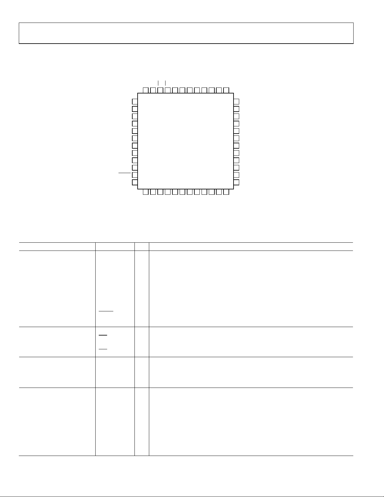
PIN CONFIGURATION AND FUNCTION DESCRIPTIONS
DVDD1
XTL_IN
XTL_OUT
DV
SS
SDATA_OUT
BIT_CLK
DV
SS
SDATA_IN
DV
DD
SYNC
RESET
NC
NC = NO CONNECT
3
3
SS
DD
NC
SPDIF
EAPD
ID1
48 47 46 45 44 43 42 41 40 39 38 37
1
2
3
4
1
5
6
7
2
8
9
2
10
11
12
13 14 15 16 17 18 19 20 21 22 23 24
AUX_L
AUX_R
PHONE_IN
ID0
AV
AD1981B
TOP VIEW
(Not to Scale)
JS1
JS0
AV
CD_L
CD_GND_REF
HP_OUT_R
CD_R
2
AV
MIC1
2
SS
DD
MONO_OUT
HP_OUT_L
AV
36
LINE_OUT_R
35
LINE_OUT_L
34
4
AV
DD
33
4
AV
SS
32
AFILT4
31
AFILT3
30
AFILT2
29
AFILT1
28
V
REFOUT
27
V
REF
26
AVSS1
25
1
AV
DD
MIC2
LINE_IN_L
LINE_IN_R
03091-009
Figure 9. 48-Lead LQFP Pin Configuration
Table 7. Pin Function Descriptions
Pin No. Mnemonic I/O Description
DIGITAL I/O
2 XTL_IN I Crystal Input (24.576 MHz) or External Clock Input.
3 XTL_OUT O Crystal Output.
5 SDATA_OUT I AC-Link Serial Data Output, AD1981B Data Input Stream.
6 BIT_CLK O/I
AC-Link Bit Clock Output (12.288 MHz) or Bit Clock Input, if Secondary Mode
Selected.
8 SDATA_IN O AC-Link Serial Data Input, AD1981B Data Output Stream.
10 SYNC I AC-Link Frame Sync.
11
RESET
I AC-Link Reset, AD1981B Master Hardware Reset.
48 SPDIF O S/PDIF Output.
CHIP SELECTS1
45
ID0
I
Chip Select Input 0 (Active Low). This pin can also be used as the chain input from a
secondary codec.
46
ID1
I Chip Select Input 1 (Active Low).
JACK SENSE AND EAPD
17 JS0 I Jack Sense 0 Input.
16 JS1 I Jack Sense 1 Input.
47 EAPD O External Amp Power-Down Control.
ANALOG I/O
13 PHONE_IN I Phone Input. Mono input from telephony subsystem speaker phone or handset.
14 AUX_L I Auxiliary Input Left Channel.
15 AUX_R I Auxiliary Input Right Channel.
18 CD_L I CD Audio Left Channel.
19 CD_GND_REF I CD Audio Analog Ground Reference for Differential CD Input.
20 CD_ R I CD Audio Right Channel.
21 MIC1 I
Microphone 1 Input (Mono) or Left Channel when 2-Channel Mode Selected
(Stereo MIC).
Rev. C | Page 10 of 32

AD1981B
Pin No. Mnemonic I/O Description
22 MIC2 I
23 LINE_IN_L I Line-In Left Channel.
24 LINE_IN_R I Line-In Right Channel.
35 LINE_OUT_L O Line-Out (Front) Left Channel.
36 LINE_OUT_R O Line-Out (Front) Right Channel.
37 MONO_OUT O Monaural Output to Telephony Subsystem Speaker Phone.
39 HP_OUT_L O Headphone Left-Channel Output.
41 HP_OUT_R O Headphone Right-Channel Output.
FILTER/REFERENCE
27 V
28 V
2
O Voltage Reference Filter.
REF
O Voltage Reference Output 5 mA Drive (Intended for MIC Bias and Power Amp Bias).
REFOUT
29 AFILT1 O Antialiasing Filter Capacitor—ADC Right Channel.
30 AFILT2 O Antialiasing Filter Capacitor—ADC Left Channel.
31 AFILT3 O Antialiasing Filter Capacitor—Mixer ADC Right Channel.
32 AFILT4 O Antialiasing Filter Capacitor—Mixer ADC Left Channel.
POWER AND GROUND SIGNALS
1 DVDD1 I Digital VDD, 3.3 V.
4 DVSS1 I Digital GND.
7 DVSS2 I Digital GND.
9 DVDD2 I Digital VDD, 3.3 V.
25 AVDD1 I Analog VDD, 5.0 V.
26 AVSS1 I Analog GND.
38 AVDD2 I Analog VDD, 5.0 V.
40 AVSS2 I Analog GND.
43 AVDD3 I Analog VDD, 5.0 V.
44 AVSS3 I Analog GND.
34 AVDD4 I Analog VDD, 5.0 V.
33 AVSS4 I Analog GND.
NO CONNECTS
12 NC No Connect.
42 NC No Connect.
1
These pins can also be used to select an external clock. See Table 44.
2
These signals are connected to resistors, capacitors, or specific voltages.
Microphone 2 Input (Mono) or Right Channel when 2-Channel Mode Selected
(Stereo MIC).
Rev. C | Page 11 of 32

AD1981B
INDEXED CONTROL REGISTERS
Table 8.
Reg Name D15 D14 D13 D12 D11 D10 D9 D8 D7 D6 D5 D4 D3 D2 D1 D0 Default
0x00 Reset X SE4 SE3 SE2 SE1 SE0 ID9 ID8 ID7 ID6 ID5 ID4 ID3 ID2 ID1 ID0 0x0090
0x02 Master
Volume
0x04 Headphone
Volume
0x06 Mono
Volume
0x0C Phone
Volume
0x0E MIC Volume MCM X X X X X X X X M20 X MCV4 MCV3 MCV2 MCV1 MCV0 0x8008
0x10 Line-In
Volume
0x12 CD Volume CVM X X LCV4 LCV3 LCV2 LCV1 LCV0 RM1X X RCV4 RCV3 RCV2 RCV1 RCV0 0x8808
0x16 AUX Volume AM X X LAV4 LAV3 LAV2 LAV1 LAV0 RM1X X RAV4 RAV3 RAV2 RAV1 RAV0 0x8808
0x18 PCM-Out
Volume
0x1A Record
Select
0x1C Record Gain IM X X X LIM3 LIM2 LIM1 LIM0 RM1X X X RIM3 RIM2 RIM1 RIM0 0x8000
0x20 General-
Purpose
0x26 Power-Down
Ctrl/Stat
0x28 Ext’d Audio
ID
0x2A Ext’d Audio
Stat/Ctrl
0x2C PCM Front
DAC Rate
0x32 PCM L/R
ADC Rate
0x3A SPDIF
Control
0x60 EQ Ctrl EQM MAD
0x62 EQ Data CFD15 CFD14 CFD13 CFD12 CFD11 CFD10 CFD9 CFD8 CFD7 CFD6 CFD5 CFD4 CFD3 CFD2 CFD1 CFD0 0x0000
0x64 Mixer ADC,
Volume
0x72 Jack Sense X X X JS MT2 JS
0x74 Serial Config SLOT 16 REG M 2 REGM 1 REGM 0 X X X CHEN X X X INTS X SPAL SPDZ SPLNK 0x7001
0x76 Misc Control
Bit
0x7C Vendor ID1 F7 F6 F5 F4 F3 F2 F1 F0 S7 S6 S5 S4 S3 S2 S1 S0 0x4144
0x7E Vendor ID2 T7 T6 T5 T4 T3 T2 T1 T0 REV7 REV6 REV5 REV4 REV3 REV2 REV1 REV0 0x5374
All registers not shown. Bits containing an X are assumed to be reserved.
Odd register addresses are aliased to the next lower even address.
Reserved registers should not be written.
Zeros should be written to reserved bits.
1
For AC ‘97 compatibility, Bit D7 (RM) is available only by setting the MSPLT bit, Register 0x76. The MSPLT bit enables separate mute bits for the left and right channels.
If MSPLT is not set, the RM bit has no effect.
MM X X LMV4 LMV3 LMV2 LMV1 LMV0 RM1X X RMV4 RMV3 RMV2 RMV1 RMV0 0x8000
HPM X X LHV4 LHV3 LHV2 LHV1 LHV0 RM1X X RHV4 RHV3 RHV2 RHV1 RHV0 0x8000
MVM X X X X X X X X X X MV4 MV3 MV2 MV1 MV0 0x8000
PHM X X X X X X X X X X PHV4 PHV3 PHV2 PHV1 PHV0 0x8008
LVM X X LLV4 LLV3 LLV2 LLV1 LLV0 RM1X X RLV4 RLV3 RLV2 RLV1 RLV0 0x8808
OM X X LOV4 LOV3 LOV2 LOV1 LOV0 RM1X X ROV4 ROV3 ROV2 ROV1 ROV0 0x8808
X X X X X LS2 LS1 LS0 X X X X X RS2 RS1 RS0 0x0000
X X X X X X MIX MS LPBK X X X X X X X 0x0000
EAPD PR6 PR5 PR4 PR3 PR2 PR1 PR0 X X X X REF ANL DAC ADC 0x000X
IDC1 IDC0 X X REVC1 REVC0 AMAP X X X DSA1 DSA0 X SPDIF X VRAS 0xX605
VFORCE X X X X SPCV X X X X SPSA1 SPSA0 X SPDIF X VRA 0x0000
SRF15 SRF14 SRF13 SRF12 SRF11 SRF10 SRF9 SRF8 SRF7 SRF6 SRF5 SRF4 SRF3 SRF2 SRF1 SRF0 0xBB80
SRA15 SRA14 SRA13 SRA12 SRA11 SRA10 SRA9 SRA8 SRA7 SRA6 SRA5 SRA4 SRA3 SRA2 SRA1 SRA0 0xBB80
V X SPSR1 SPSR0 L CC6 CC5 CC4 CC3 CC2 CC1 CC0 PRE COPY /AUD PRO 0x2000
X X X X X X SYM CHS BCA5 BCA4 BCA3 BCA2 BCA1 BCA0 0x8080
LBEN
MXM X X X LMG3 LMG2 LMG1 LMG0 RM1X X X RMG3 RMG2 RMG1 RMG0 0x8000
JS
JS1
JS0
JS1
JS0
JS1
JS0
JS1
MT1
MT0
EQB
EQB
TMR
DACZ X MSPLT LODIS DAM X FMXE X MAD
PD
TMR
MD
MD
2CMIC X MAD
ST
JS0 ST JS1
ST
VREFH VREFD MBG1 MBG0 0x0000
INT
JS0
INT
0x0000
Rev. C | Page 12 of 32

AD1981B
CONTROL REGISTER DETAILS
RESET REGISTER
Index 0x00
Reg No. Name D15 D14 D13 D12 D11 D10 D9 D8 D7 D6 D5 D4 D3 D2 D1 D0 Default
0x00 Reset X SE4 SE3 SE2 SE1 SE0 ID9 ID8 ID7 ID6 ID5 ID4 ID3 ID2 ID1 ID0 0x0090
X is a wild card and has no effect on the value.
Writing any value to this register performs a register reset that causes all registers to revert to their default values (except 0x74, which forces the serial configuration).
Reading this register returns the ID code of the part and a code for the type of 3D stereo enhancement.
SE[4:0] Stereo Enhancement. The AD1981B does not provide hardware 3D stereo enhancement (all bits are 0s).
ID[9:0] Identify Capability. The ID decodes the capabilities of AD1981B based on the functions listed in Table 9.
Table 9. ID Bits
Bit Function AD1981B
ID0 Dedicated MIC PCM in Channel 0
ID1 Modem Line Codec Support 0
ID2 Bass and Treble Control 0
ID3 Simulated Stereo (Mono to Stereo) 0
ID4 Headphone Out Support 1
ID5 Loudness (Bass Boost) Support 0
ID6 18-Bit DAC Resolution 0
ID7 20-Bit DAC Resolution 1
ID8 18-Bit ADC Resolution 0
ID9 20-Bit ADC Resolution 0
MASTER VOLUME REGISTER
Index 0x02
This register controls the Line_Out volume controls for both stereo channels and the mute bit. Each volume subregister contains five bits,
generating 32 volume levels with 31 steps of 1.5 dB each. Because AC ’97 defines 6-bit volume registers, to maintain compatibility
whenever the D5 or D13 bits are set to 1, their respective lower five volume bits are automatically set to 1 by the codec logic. On readback,
all lower five bits read 1s whenever these bits are set to 1. Refer to Table 12 for examples.
Reg No. Name D15 D14 D13 D12 D11 D10 D9 D8 D7 D6 D5 D4 D3 D2 D1 D0 Default
0x02
Master
Volume
MM X X LMV4 LMV3 LMV2 LMV1 LMV0
1
For AC ‘97 compatibility, Bit D7 (RM) is available only by setting the MSPLT bit, Register 0x76. The MSPLT bit enables separate mute bits for the left and right channels.
If MSPLT is not set, the RM bit has no effect. All registers are not shown, and bits containing an X are assumed to be reserved.
Table 10.
Bit Mnemonic Function
RMV [4:0]
RM Right-Channel Mute
Right Master Volume
Control
The least significant bit represents 1.5 dB. This register controls the output from 0 dB to a maximum
attenuation of 46.5 dB.
Once enabled by the MSPLT bit in Register 0x76, this bit mutes the right channel separately from the
MM bit. Otherwise, this bit always reads 0 and has no effect when set to 1.
LMV [4:0]
MM Master Volume Mute
Left Master Volume
Control
The least significant bit represents 1.5 dB. This register controls the output from 0 dB to a maximum
attenuation of 46.5 dB.
When this bit is set to 1, both the left and right channels are muted, unless the MSPLT bit in
Register 0x76 is set to 1, in which case this mute bit affects only the left channel.
1
X X RMV4 RMV3 RMV2 RMV1 RMV0 0x8000
RM
Rev. C | Page 13 of 32

AD1981B
HEADPHONE VOLUME REGISTER
Index 0x04
This register controls the headphone volume controls for both stereo channels and the mute bit. Each volume subregister contains five
bits, generating 32 volume levels with 31 steps of 1.5 dB each. Because AC ’97 defines 6-bit volume registers, to maintain compatibility,
whenever the D5 or D13 bits are set to 1, their respective lower five volume bits are automatically set to 1 by the codec logic. On readback,
all lower five bits read 1s whenever these bits are set to 1. Refer to Table 12 for examples.
Reg
Name D15 D14 D13 D12 D11 D10 D9 D8 D7 D6 D5 D4 D3 D2 D1 D0 Default
No.
0x04
Headphone
Volume
1
For AC ’97 compatibility, Bit D7 (RM) is available only by setting the MSPLT bit, Register 0x76. The MSPLT bit enables separate mute bits for the left and right channels.
If MSPLT is not set, the RM bit has no effect. All registers are not shown, and bits containing an X are assumed to be reserved.
Table 11.
Bit Mnemonic Function
RHV [4:0]
RM Right-Channel Mute
LHV [4:0]
HPM
Table 12. Volume Settings for Master and Headphone
Reg. 0x76 Control Bits Master Volume (0x02) and Headphone Volume (0x04)
1
MSPLT
0 0 00 0000 00 0000 0 dB Gain X 00 0000 00 0000 0 dB Gain
0 0 00 1111 00 1111 −22.5 dB Gain X 00 1111 00 1111 −22.5 dB Gain
0 0 01 1111 01 1111 −46.5 dB Gain X 01 1111 01 1111 −46.5 dB Gain
0 0 1X XXXX 01 1111 −46.5 dB Gain X 1X XXXX 01 1111 −46.5 dB Gain
0 1 XX XXXX XX XXXX −∞ dB Gain, Muted X XX XXXX XX XXXX −∞ dB Gain, Muted
1 0 1X XXXX 01 1111 −46.5 dB Gain 1 XX XXXX XX XXXX −∞ dB Gain, Right Only Muted
1 1 XX XXXX XX XXXX −∞ dB Gain, Left Only Muted 0 XX XXXX XX XXXX −46.5 dB Gain
1 1 XX XXXX XX XXXX −∞ dB Gain, Left Muted 1 XX XXXX XX XXXX −∞ dB Gain, Right Muted
1
For AC ’97 compatibility, Bit D7 (RM) is available only by setting the MSPLT bit, Register 0x76. The MSPLT bit enables separate mute bits for the left and right channels.
If MSPLT is not set, the RM bit has no effect.
X is a wild card and has no effect on the value.
HPM X X LHV4 LHV3 LHV2 LHV1 LHV0 RM1X X RHV4 RHV3 RHV2 RHV1 RHV0 0x8000
Right Headphone
Volume Control
The least significant bit represents 1.5 dB. This register controls the output from 0 dB to a maximum
attenuation of 46.5 dB.
Once enabled by the MSPLT bit in Register 0x76, this bit mutes the right channel separately from the
HPM bit. Otherwise, this bit always reads 0 and has no effect when set to 1.
Left Headphone
Volume Control
Headphone Volume
Mute
D15 Write Readback Function
The least significant bit represents 1.5 dB. This register controls the output from 0 dB to a maximum
attenuation of 46.5 dB.
When this bit is set to 1, both the left and right channels are muted, unless the MSPLT bit in
Register 0x76 is set to 1, in which case this mute bit affects only the left channel.
Left-Channel Volume D [13:8] Right-Channel Volume D [5:0]
Write Readback Function
D71
Rev. C | Page 14 of 32

AD1981B
MONO VOLUME REGISTER
Index 0x06
This register controls the mono output volume and mute bit. The volume register contains five bits, generating 32 volume levels with
31 steps of 1.5 dB each. Because AC ’97 defines 6-bit volume registers, to maintain compatibility, whenever the D5 bit is set to 1, their
respective lower five volume bits are automatically set to 1 by the codec logic. On readback, all lower five bits read 1s whenever this bit is
set to 1. Refer to Table 14 for examples.
Reg No. Name D15 D14 D13 D12 D11 D10 D9 D8 D7 D6 D5 D4 D3 D2 D1 D0 Default
0x06 Mono Volume MVM X X X X X X X X X X MV4 MV3 MV2 MV1 MV0 0x8000
All registers are not shown, and bits containing an X are assumed to be reserved.
Table 13.
Bit Mnemonic Function
MV [4:0] Mono Volume Control
MVM Mono Volume Mute When this bit is set to 1, the channel is muted.
Table 14. Volume Settings for Mono
D15
Write Readback
0 0000 0 0000 0 dB Gain
0 0 1111 0 1111 −22.5 dB Gain
0 1 1111 1 1111 −46.5 dB Gain
1 X XXXX X XXXX −∞ dB Gain, Muted
An X is a wild card and has no effect on the value.
The least significant bit represents 1.5 dB. This register controls the output from 0 dB to a maximum
attenuation of 46.5 dB.
Control Bits D [4:0] for Mono (0x06)
Function
PHONE VOLUME REGISTER
Index 0x0C
Reg No. Name D15 D14 D13 D12 D11 D10 D9 D8 D7 D6 D5 D4 D3 D2 D1 D0 Default
0x0C Phone Volume PHM X X X X X X X X X X PHV4 PHV3 PHV2 PHV1 PHV0 0x8008
All registers are not shown, and bits containing an X are assumed to be reserved. Refer to Table 17 for examples.
Table 15.
Bit Mnemonic Function
PHV [4:0] Phone Volume
PHM Phone Mute When this bit is set to 1, the phone channel is muted.
All registers are not shown, and bits containing an X are assumed to be reserved. Refer to Table 17 for examples.
Allows setting the phone volume attenuator in 32 volume levels with 31 steps of 1.5 dB each. The
LSB represents 1.5 dB, and the gain range is +12 dB to −34.5 dB. The default value is 0 dB, with the
mute bit enabled.
Rev. C | Page 15 of 32

AD1981B
MIC VOLUME REGISTER
Index 0x0E
Reg No. Name D15 D14 D13 D12 D11 D10 D9 D8 D7 D6 D5 D4 D3 D2 D1 D0 Default
0x0E MIC Volume MCM X X X X X X X X M20 X MCV4 MCV3 MCV2 MCV1 MCV0 0x8008
All registers are not shown, and bits containing an X are assumed to be reserved. Refer to Table 17 for examples.
Table 16.
Bit Mnemonic Function
MCV [4:0] MIC Volume Gain
M20 MIC Gain Boost
MCM MIC Mute When this bit is set to 1, the MIC channel is muted.
Table 17. Volume Settings for Phone and MIC
D15
0 0 0000 0 0000 12 dB Gain
0 0 1000 0 1000 0 dB Gain
0 1 1111 1 1111 −34.5 dB Gain
1 X XXXX X XXXX −∞ db Gain, Muted
X is a wild card, and has no effect on the value.
Allows setting the phone volume attenuator in 32 volume levels with 31 steps of 1.5 dB each. The LSB
represents 1.5 dB, and the gain range is +12 dB to −34.5 dB. The default value is 0 dB, with the mute bit
enabled.
This bit allows setting additional MIC gain to increase the microphone sensitivity. The nominal gain
boost by default is 20 dB; however, Bits D0 and D1 (MBG [1:0]) on the miscellaneous control bits register
(0x76) allow changing the gain boost to 10 dB or 30 dB, if necessary.
0 = Disabled; Gain = 0 dB
1 = Enabled; Default Gain = 20 dB (see Register 0x76, Bits D0, D1)
Control Bits D [4:0] Phone (0x0C) and MIC (0x0E)
Write Readback
Function
LINE-IN VOLUME REGISTER
Index 0x10
Reg No. Name D15 D14 D13 D12 D11 D10 D9 D8 D7 D6 D5 D4 D3 D2 D1 D0 Default
0x10 Line-In Volume LVM X X LLV4 LLV3 LLV2 LLV1 LLV0 RM1X X RLV4 RLV3 RLV2 RLV1 RLV0 0x8808
1
For AC ’97 compatibility, Bit D7 (RM) is available only by setting the MSPLT bit, Register 0x76. The MSPLT bit enables separate mute bits for the left and right channels.
If MSPLT is not set, the RM bit has no effect. All registers are not shown, and bits containing an X are assumed to be reserved. Refer to for examples.
Table 18.
Bit Mnemonic Function
RLV [4:0] Line-In Volume Right
Allows setting the line-in right-channel attenuator in 32 volume levels. The LSB represents 1.5 dB, and
the range is +12 dB to −34.5 dB. The default value is 0 dB, mute enabled.
RM Right-Channel Mute
Once enabled by the MSPLT bit in Register 0x76, this bit mutes the right channel separately from the
LM bit. Otherwise, this bit always reads 0 and has no effect when set to 1.
LLV [4:0] Line-In Volume Left
Allows setting the line-in left-channel attenuator in 32 volume levels. The LSB represents 1.5 dB, and
the range is +12 dB to −34.5 dB. The default value is 0 dB, mute enabled.
LVM Line-In Mute
When this bit is set to 1, both the left and right channels are muted, unless the MSPLT bit in
Register 0x76 is set to 1, in which case this mute bit affects only the left channel.
Table 22
Rev. C | Page 16 of 32

AD1981B
CD VOLUME REGISTER
Index 0x12
Reg No. Name D15 D14 D13 D12 D11 D10 D9 D8 D7 D6 D5 D4 D3 D2 D1 D0 Default
0x12 CD Volume CVM X X LCV4 LCV3 LCV2 LCV1 LCV0 RM1 X X RCV4 RCV3 RCV2 RCV1 RCV0 0x8808
1
For AC ‘97 compatibility, Bit D7 (RM) is available only by setting the MSPLT bit, Register 0x76. The MSPLT bit enables separate mute bits for the left and right channels.
If MSPLT is not set, the RM bit has no effect. All registers are not shown, and bits containing an X are assumed to be reserved. Refer to
Table 19.
Bit Mnemonic Function
RCV [4:0] Right CD Volume
Allows setting the CD right-channel attenuator in 32 volume levels. The LSB represents 1.5 dB, and the
gain range is +12 dB to −34.5 dB. The default value is 0 dB, mute enabled.
RM Right-Channel Mute
Once enabled by the MSPLT bit in Register 0x76, this bit mutes the right channel separately from the
CVM bit. Otherwise, this bit always reads 0 and has no affect when set to 1.
LCV [4:0] Left CD Volume
Allows setting the CD left-channel attenuator in 32 volume levels. The LSB represents 1.5 dB, and the
gain range is +12 dB to −34.5 dB. The default value is 0 dB, mute enabled.
CVM CD Volume Mute
When this bit is set to 1, both the left and right channels are muted, unless the MSPLT bit in
Register 0x76 is set to 1, in which case this mute bit affects only the left channel.
AUX VOLUME REGISTER
Index 0x16
Reg No. Name D15 D14 D13 D12 D11 D1 D9 D8 D7 D6 D5 D4 D3 D2 D1 D0 Default
0x16 AUX Volume AM X X LAV4 LAV3 LAV2 LAV1 LAV0 RM1X X RAV4 RAV3 RAV2 RAV1 RAV0 0x8808
1
For AC ’97 compatibility, Bit D7 (RM) is available only by setting the MSPLT bit, Register 0x76. The MSPLT bit enables separate mute bits for the left and right channels.
If MSPLT is not set, the RM bit has no effect. All registers are not shown, and bits containing an X are assumed to be reserved. Refer to for examples.
Table 20.
Bit Mnemonic Function
RAV [4:0] Right AUX Volume
RM Right-Channel Mute
LAV [4:0] Left AUX Volume
AM AUX Volume Mute
Allows setting the AUX right-channel attenuator in 32 volume levels. The LSB represents 1.5 dB, and
the gain range is +12 dB to −34.5 dB. The default value is 0 dB, mute enabled.
Once enabled by the MSPLT bit in Register 0x76, this bit mutes the right channel separately from the
AM bit. Otherwise, this bit always reads 0 and has no affect when set to 1.
Allows setting the AUX left-channel attenuator in 32 volume levels. The LSB represents 1.5 dB, and
the gain range is +12 dB to −34.5 dB. The default value is 0 dB, mute enabled.
When this bit is set to 1, both the left and right channels are muted, unless the MSPLT bit in
Register 0x76 is set to 1, in which case this mute bit affects only the left channel.
Table 22 for examples.
Table 22
Rev. C | Page 17 of 32

AD1981B
PCM-OUT VOLUME REGISTER
Index 0x18
Reg
No.
0x18
1
Table 21.
Bit Mnemonic Function
ROV [4:0] Right PCM-Out Volume
RM Right-Channel Mute
LOV [4:0] Left PCM-Out Volume
OM PCM-Out Volume Mute
Table 22. Volume Settings for Line-In, CD Volume, AUX, and PCM-Out
Reg. 0x76
MSPLT
0 0 0 0000 0 0000 +12 dB Gain X 0 0000 0 0000 +12 dB Gain
0 0 0 1000 0 1000 0 dB Gain X 0 1000 0 1000 0 dB Gain
0 0 1 1111 1 1111
0 1 X XXXX X XXXX
1 0 1 1111 1 1111
1 1 X XXXX X XXXX
1 1 X XXXX X XXXX
1
X is a wild card and has no effect on the value.
Name D15 D14 D13 D12 D11 D10 D9 D8 D7 D6 D5 D4 D3 D2 D1 D0 Default
PCM-Out
Volume
For AC ’97 compatibility, Bit D7 (RM) is available only by setting the MSPLT bit, Register 0x76. The MSPLT bit enables separate mute bits for the left and right channels.
If MSPLT is not set, the RM bit has no effect. All registers are not shown, and bits containing an X are assumed to be reserved. Refer to for examples. Table 22
OM X X LOV4 LOV3 LOV2 LOV1 LOV0 RM1X X ROV4 ROV3 ROV2 ROV1 ROV0 0x8808
Allows setting the PCM right-channel attenuator in 32 volume levels. The LSB represents 1.5 dB, and
the range is +12 dB to −34.5 dB. The default value is 0 dB, mute enabled.
Once enabled by the MSPLT bit in Register 0x76, this bit mutes the right channel separately from
the OM bit. Otherwise, this bit always reads 0 and has no effect when set to 1.
Allows setting the PCM left-channel attenuator in 32 volume levels. The LSB represents 1.5 dB, and
the range is +12 dB to −34.5 dB. The default value is 0 dB, mute enabled.
When this bit is set to 1, both the left and right channels are muted unless the MSPLT bit in
Register 0x76 is set to 1, in which case this mute bit affects only the left channel.
Control Bits
Line-In (0x10), CD (0x12), AUX (0x16), and PCM-Out (0x18)
Left-Channel Volume D [12:8] Right-Channel Volume D [4:0]
1
D15 Write Readback Function D71 Write Readback Function
+34.5 dB
Gain
−∞ dB Gain,
Muted
−34.5 dB
Gain
X 1 1111 1 1111
X X XXXX X XXXX
1 X XXXX X XXXX
−34.5 dB
Gain
−∞ dB Gain,
Muted
−∞ dB Gain,
Right Only
Muted
−∞ dB Gain,
Left Only
0 1 1111 1 1111
−34.5 dB
Gain
Muted
−∞ dB Gain,
Left Muted
For AC ’97 compatibility, Bit D7 (RM) is available only by setting the MSPLT bit, Register 0x76. The MSPLT bit enables separate mute bits for the left and right channels.
If MSPLT is not set, the RM bit has no effect.
1 X XXXX X XXXX
−∞ dB Gain,
Right Muted
Rev. C | Page 18 of 32

AD1981B
RECORD SELECT CONTROL REGISTER
Index 0x1A
Reg No. Name D15 D14 D13 D12 D11 D10 D9 D8 D7 D6 D5 D4 D3 D2 D1 D0 Default
0x1A Record Select X X X X X LS2 LS1 LS0 X X X X X RS2 RS1 RS0 0x0000
All registers are not shown, and bits containing an X are assumed to be reserved. Used to select the record source independently for right and left. The default value is
0x0000, which corresponds to MIC In. Refer to Table 24 for examples.
Table 23.
Bit Function
RS [2:0] Right Record Select
LS [2:0] Left Record Select
Table 24. Settings for Record Select Control
LS [10:8] Left Record Source RS [2:0] Right Record Source
000 MIC 000 MIC
001 CD_L 001 CD_R
010 Muted 010 Muted
011 AUX_L 011 AUX_R
100 LINE_IN_L 100 LINE_IN_R
101 Stereo Mix (L) 101 Stereo Mix (R)
110 Mono Mix 110 Mono Mix
111 PHONE_IN 111 PHONE_IN
RECORD GAIN REGISTER
Index 0x1C
Reg No. Name D15 D14 D13 D12 D11 D10 D9 D8 D7 D6 D5 D4 D3 D2 D1 D0 Default
0x1C Record Gain IM X X X LIM3 LIM2 LIM1 LIM0 RM1X X X RIM3 RIM2 RIM1 RIM0 0x8000
1
For AC ’97 compatibility, Bit D7 (RM) is available only by setting the MSPLT bit, Register 0x76. The MSPLT bit enables separate mute bits for the left and right channels.
If MSPLT is not set, the RM bit has no effect. All registers are not shown, and bits containing an X are assumed to be reserved. Refer to Table 24 for examples.
Table 25.
Bit Mnemonic Function
RIM [3:0]
Right Input Mixer Gain
Control
RM Right-Channel Mute
LIM [3:0]
Left Input Mixer Gain
Control
IM Input Mute
Each LSB represents 1.5 dB, 0000 = 0 dB, and the gain range is 0 dB to 22.5 dB.
Once enabled by the MSPLT bit in Register 0x76, this bit mutes the right channel separately from the
IM bit. Otherwise, this bit always reads 0 and has no affect when set to 1.
Each LSB represents 1.5 dB, 0000 = 0 dB, and the gain range is 0 dB to 22.5 dB.
When this bit is set to 1, both the left and right channels are muted, unless the MSPLT bit in
Register 0x76 is set to 1, in which case this mute bit affects only the left channel.
Rev. C | Page 19 of 32

AD1981B
Table 26. Settings for Record Gain Register
Reg. 0x76 Control Bits Record Gain (1Channel)
Left-Channel Input Mixer D [11:8] Right-Channel Input Mixer D [3:0]
MSPLT1
D15 Write Readback Function D7
0 0 1111 1111 22.5 dB Gain X 1111 1111 22.5 dB Gain
0 0 0000 0000 0 dB Gain X 0000 0000 0 dB Gain
0 1 XXXX XXXX
−∞ dB Gain,
Muted
1 0 1111 1111 22.5 dB Gain 1 XXXX XXXX
1 1 XXXX XXXX
−∞ dB Gain,
Left Only
Muted
1 1 XXXX XXXX
−∞ dB Gain,
Left Muted
1
For AC ’97 compatibility, Bit D7 (RM) is available only by setting the MSPLT bit, Register 0x76. The MSPLT bit enables separate mute bits for the left and right channels.
If MSPLT is not set, the RM bit has no effect.
X is a wild card and has no effect on the value.
GENERAL-PURPOSE REGISTER
Index 0x20
Reg No. Name D15 D14 D13 D12 D11 D10 D9 D8 D7 D6 D5 D4 D3 D2 D1 D0 Default
0x20 General-Purpose X X X X X X MIX MS LPBK X X X X X X X 0x0000
This register should be read before writing to generate a mask for only the bit(s) that need to be changed.
All registers are not shown, and bits containing an X are assumed to be reserved.
Table 27.
Bit Mnemonic Function
LPBK Loopback Control ADC/DAC Digital Loopback Mode.
0 = No Loopback (default).
1 = Loopback PCM Digital Data from ADC Output to DAC.
MS MIC Select Selects mono MIC input.
0 = Select MIC1.
1 = Select MIC2.
See the 2CMIC bit in Register 0x76 to enable stereo microphone recording.
MIX Mono Output Select Selects mono output audio source.
0 = Mixer Mono Output (reset default).
1 = MIC1 Channel.
1
Write Readback Function
X XXXX XXXX
−∞ dB Gain,
Muted
−∞ dB Gain,
Right Only
Muted
0 1111 1111 22.5 dB Gain
1 XXXX XXXX
−∞ dB Gain,
Right Muted
Rev. C | Page 20 of 32

AD1981B
POWER-DOWN CONTROL/STATUS REGISTER
Index 0x26
Reg No. Name D15 D14 D13 D12 D11 D10 D9 D8 D7 D6 D5 D4 D3 D2 D1 D0 Default
0x26 Power-Down Ctrl/Stat EAPD PR6 PR5 PR4 PR3 PR2 PR1 PR0 X X X X REF ANL DAC ADC 0x000X
The ready bits are read-only; writing to REF, ANL, DAC, ADC has no effect. These bits indicate the status for the AD1981B subsections. If the bit is a 1, that subsection is
ready. Ready is defined as the subsection able to perform in its nominal state.
All registers are not shown, and bits containing an X are assumed to be reserved.
Table 28.
Bit Mnemonic Function
ADC ADC Sections Ready to Transmit Data.
DAC DAC Sections Ready to Accept Data.
ANL Analog Amplifiers, Attenuators, and Mixers Ready.
REF Voltage References, V
PR [6:0]
Codec PowerDown Modes
The first three bits are to be used individually rather than in combination with each other. PR3 can be
used in combination with PR2 or by itself. The mixer and reference cannot be powered down via PR3
unless the ADCs and DACs are also powered down.
Nothing else can be powered up until the reference is powered up. PR5 has no effect unless all ADCs,
DACs, and the ac-link are powered down. The reference and the mixer can be either powered up or
powered down, but all power-up sequences must be allowed to run to completion before PR5 and PR4
are both set.
In multiple codec systems, the master codec’s PR5 and PR4 bits control the slave codec. PR5 is also
effective in the slave codec, if the master’s PR5 bit is clear, but the PR4 bit has no effect except to enable or
disable PR5.
EAPD
External Audio
Power-Down
Control
Controls the state of the EAPD pin.
EAPD = 0 sets the EAPD pin low, enabling an external power amplifier (reset default).
EAPD = 1 sets the EAPD pin high, shutting the external power amplifier off.
Table 29.
Power-Down State Set Bits PR [6:0]
ADCs and Input MUX Power-Down PR0 [000 0001]
DACs Power-Down PR1 [000 0010]
Analog Mixer Power-Down (V
Analog Mixer Power-Down (V
REF
REF
and V
and V
On) PR1, PR2 [000 0101]
REFOUT
Off) PR0, PR1, PR3 [000 1011]
REFOUT
AC-Link Interface Power-Down PR4 [001 0000]
Internal Clocks Disabled PR0, PR1, PR4, PR5 [011 0011]
ADC and DAC Power-Down PR0, PR1 [000 0011]
V
Standby Mode PR0, PR1, PR2, PR4, PR5 [011 0111]
REF
Total Power-Down PR0, PR1, PR2, PR3, PR4, PR5, PR6 [111 1111]
Headphone Amp Power-In Standby PR6 [100 0000]
REF
and V
, Up to Nominal Level.
REFOUT
Rev. C | Page 21 of 32

AD1981B
EXTENDED AUDIO ID REGISTER
Index 0x28
Reg No. Name D15 D14 D13 D12 D11 D10 D9 D8 D7 D6 D5 D4 D3 D2 D1 D0 Default
0x28 Ext’d Audio ID IDC1 IDC0 X X REVC1 REVC0 AMAP X X X DSA1 DSA0 X SPDIF X VRAS 0xX605
The extended audio ID register identifies which extended audio features are supported. A nonzero extended audio ID value indicates that one or more of the
extended audio features are supported.
All registers are not shown, and bits containing an X are assumed to be reserved.
Table 30.
Bit Mnemonic Function
VRAS
Variable Rate PCM Audio
Support (Read-Only)
SPDIF SPDIF Support (Read-Only) This bit returns a 1 when Read To indicates that the SPDIF transmitter is supported (IEC958).
DSA [1:0]
DAC Slot Assignments
(Read/Write)
AMAP
Slot DAC Mappings Based
on Codec ID (Read-Only)
REVC [1:0] AC ’97 Revision Compliance REVC [1:0] = 01 indicates that the codec is AC ’97 revision 2.2 compliant (read-only).
IDC [1:0]
Indicates Codec
Configuration (Read-Only)
This bit returns a 1 when Read To indicates that the variable rate PCM audio is supported.
This bit is also used to validate that the SPDIF transmitter output is enabled. The SPDIF bit can
be set high only if the SPDIF pin (Pin 48) is pulled down at power-up, enabling the codec
transmitter logic. If the SPDIF pin is floating or pulled high at power-up, the transmitter logic
is disabled; therefore, this bit returns a low, indicating that the SPDIF transmitter is not
available. This bit must always be read back to verify that the SPDIF transmitter is actually
enabled.
Reset default = 00.
00 DACs 1, 2 = 3 and 4.
01 DACs 1, 2 = 7 and 8.
10 DACs 1, 2 = 6 and 9.
11 Reserved.
This bit returns a 1 when read to indicate that slot/DAC mappings based on the codec ID are
supported.
00 = Primary.
01, 10, 11 = Secondary.
EXTENDED AUDIO STATUS AND CONTROL REGISTER
Index 0x2A
Reg
No.
0x2A
All registers are not shown, and bits containing an X are assumed to be reserved.
The extended audio status and control register is a read/write register that provides status and control of the extended audio features.
Table 31.
Bit Mnemonic Function
VRA
SPDIF
SPSA [1:0]
Name D15 D14 D13 D12 D11 D10 D9 D8 D7 D6 D5 D4 D3 D2 D1 D0 Default
Ext’d Audio
Stat/Ctrl
Variable Rate Audio
(Read/Write)
VFORCE X X X X SPCV X X X X SPSA1 SPSA0 X SPDIF X VRA 0x0000
VRA = 0 sets the fixed sample rate audio to 48 kHz (reset default).
VRA = 1 enables variable rate audio mode (enables sample rate registers and SLOTREQ
signaling).
SPDIF Transmitter
Subsystem Enable/Disable
Bit (Read/Write)
SPDIF = 1 enables the SPDIF transmitter.
SPDIF = 0 disables the SPDIF transmitter (default).
This bit is also used to validate that the SPDIF transmitter output is enabled. The SPDIF bit can
be set high only if the SPDIF pin (Pin 48) is pulled down at power-up, enabling the codec
transmitter logic. If the SPDIF pin is floating or pulled high at power-up, the transmitter logic is
disabled and this bit returns a low, indicating that the SPDIF transmitter is not available. This bit
must always be read back to verify that the SPDIF transmitter is enabled.
SPDIF Slot Assignment Bits
(Read/Write)
These bits control the SPDIF slot assignment and respective defaults, depending on the codec
ID configuration.
Rev. C | Page 22 of 32

AD1981B
Bit Mnemonic Function
SPCV
VFORCE
Table 32. AC ’97 2.2 AMAP-Compliant Default SPDIF Slot Assignments
Codec ID Function SPSA = 00 SPSA = 01 SPSA = 10 SPSA = 11
00 2-Channel Primary w/SPDIF 3 and 4 7 and 8 (default) 6 and 9 10 and 11
00 4-Channel Primary w/SPDIF 3 and 4 7 and 8 6 and 9 (default) 10 and 11
00 6-Channel Primary w/SPDIF 3 and 4 7 and 8 6 and 9 10 and 11 (default)
01 +2-Channel Secondary w/SPDIF 3 and 4 7 and 8 6 and 9 (default)
01 +4-Channel Secondary w/SPDIF 3 and 4 7 and 8 6 and 9 10 and 11 (default)
10 +2-Channel Secondary w/SPDIF 3 and 4 7 and 8 6 and 9 (default)
10 +4-Channel Secondary w/SPDIF 3 and 4 7 and 8 6 and 9 10 and 11 (default)
11 +2-Channel Secondary w/SPDIF 3 and 4 7 and 8 6 and 9 10 and 11 (default)
SPDIF Configuration Valid
(Read-Only)
Validity Force Bit
(Reset Default = 0)
This bit indicates the status of the SPDIF transmitter subsystem, enabling the driver to
determine if the currently programmed SPDIF configuration is supported. SPCV is always valid,
independent of the SPDIF enable bit status.
SPCV = 0 indicates that the current SPDIF configuration (SPSA, SPSR, DAC slot rate, DRS) is not
valid (not supported).
SPCV = 1 indicates that the current SPDIF configuration (SPSA, SPSR, DAC slot rate, DRS) is valid
(supported).
When asserted, this bit forces the SPDIF stream validity flag (Bit 28 within each SPDIF L/R
subframe) to be controlled by the V bit (D15) in Register 0x3A (SPDIF control register).
VFORCE = 0 and V = 0; the validity bit is managed by the codec error detection logic.
VFORCE = 0 and V = 1; the validity bit is forced high, indicating the subframe data is invalid.
VFORCE = 1 and V = 0; the validity bit is forced low, indicating the subframe data is valid.
VFORCE = 1 and V = 1; the validity bit is forced high, indicating the subframe data is invalid.
PCM FRONT DAC RATE REGISTER
Index 0x2C
Reg
Name D15 D14 D13 D12 D11 D10 D9 D8 D7 D6 D5 D4 D3 D2 D1 D0 Default
No.
0x2C
PCM
Front
DAC
Rate
This read/write sample rate control register contains a 16-bit unsigned value, representing the rate of operation in Hz.
SRF15 SRF14 SRF13 SRF12 SRF11 SRF10 SRF9 SRF8 SRF7 SRF6 SRF5 SRF4 SRF3 SRF2 SRF1 SRF0 0xBB80
Table 33.
Bit Mnemonic Function
SRF [15:0] Sample Rate
The sampling frequency range is from 7 kHz (0x1B58) to 48 kHz (0xBB80) in 1 Hz increments. If 0 is written to
VRA, the sample rate is reset to 48 kHz.
PCM ADC RATE REGISTER
Index 0x32
Reg
No.
Name D15 D14 D13 D12 D11 D10 D9 D8 D7 D6 D5 D4 D3 D2 D1 D0 Default
0x32 PCM L/R
ADC
Rate
This read/write sample rate control register contains a 16-bit unsigned value, representing the rate of operation in Hz.
Table 34.
Bit Mnemonic Function
SRA
[15:0]
SRA15 SRA14 SRA13 SRA12 SRA11 SRA10 SRA9 SRA8 SRA7 SRA6 SRA5 SRA4 SRA3 SRA2 SRA1 SRA0 0xBB80
Sample Rate
The sampling frequency range is from 7 kHz (0x1B58) to 48 kHz (0xBB80) in 1 Hz increments. If 0 is written to
VRA, the sample rate is reset to 48 kHz.
Rev. C | Page 23 of 32

AD1981B
SPDIF CONTROL REGISTER
Index 0x3A
Reg No. Name D15 D14 D13 D12 D11 D10 D9 D8 D7 D6 D5 D4 D3 D2 D1 D0 Default
0x3A SPDIF Control V X SPSR1 SPSR0 L CC6 CC5 CC4 CC3 CC2 CC1 CC0 PRE COPY
Register 0x3A is a read/write register that controls SPDIF functionality and manages bit fields propagated as channel status (or subframe in the V case). With the
exception of V, this register should be written to only when the SPDIF transmitter is disabled (SPDIF bit in Register 0x2A is 0). This ensures that control and status
information start up correctly at the beginning of SPDIF transmission.
Table 35.
Bit Mnemonic Function
PRO Professional 1 = Professional use of channel status.
0 = Consumer.
AUD
Nonaudio 1 = Data is non-PCM format.
0 = Data is PCM format.
COPY Copyright 1 = Copyright is asserted.
0 = Copyright is not asserted.
PRE Pre-emphasis 1 = Filter pre-emphasis is 50 µs/15 µs.
0 = Pre-emphasis is none.
CC [6:0] Category Code Programmed according to IEC standards, or as appropriate.
L Generation Level Programmed according to IEC standards, or as appropriate.
SPSR [1:0]
SPDIF Transmit
Sample Rate
SPSR [1:0] = 00: Transmit sample rate is 44.1 kHz.
SPSR [1:0] = 01: Reserved.
SPSR [1:0] = 10: Transmit sample rate is 48 kHz (reset default).
SPSR [1:0] = 11: Not supported.
V Validity
This bit affects the validity flag (Bit 28 transmitted in each SPDIF L/R subframe) and enables the SPDIF
transmitter to maintain connection during error or mute conditions.
V = 1: Each SPDIF subframe (L + R) has Bit 28 set to 1. This tags both samples as invalid.
V = 0: Each SPDIF subframe (L + R) has Bit 28 set to 0 for valid data and 1 for invalid data (error
condition).
When V = 0, asserting the VFORCE bit (D15) in Register 0x2A (Ext’d Audio Stat/Ctrl) forces the validity
flag low, marking both samples as valid.
AUD
PRO 0x2000
EQ CONTROL REGISTER
Index 0x60
Reg No. Name D15 D14 D13 D12 D11 D10 D9 D8 D7 D6 D5 D4 D3 D2 D1 D0 Default
0x60 EQ Ctrl EQM MAD LBEN X X X X X X SYM CHS BCA5 BCA4 BCA3 BCA2 BCA1 BCA0 0x8080
Register 0x60 is a read/write register that controls the equalizer functionality and data setup. This register contains the biquad and coefficient address pointer, which
is used in conjunction with the EQ data register (0x78) to set up the equalizer coefficients. The reset default disables the equalizer function until the coefficients can be
properly set up by the software and sets the symmetry bit to allow equal coefficients for left and right channels.
All registers are not shown, and bits containing an X are assumed to be reserved.
Table 36.
Bit Mnemonic Function
BCA [5:0]
Biquad and Coefficient
Address Pointer
biquad 0 coef a1 BCA[5:0] = 011010
biquad 0 coef a2 BCA[5:0] = 011001
biquad 0 coef b1 BCA[5:0] = 011101
biquad 0 coef b2 BCA[5:0] = 011100
biquad 1 coef a0 BCA[5:0] = 100000
biquad 1 coef a1 BCA[5:0] = 011111
biquad 0 coef a0 BCA[5:0] = 011011
Rev. C | Page 24 of 32

AD1981B
Bit Mnemonic Function
biquad 1 coef a2 BCA[5:0] = 011110
biquad 1 coef b1 BCA[5:0] = 100010
biquad 1 coef b2 BCA[5:0] = 100001
biquad 2 coef a0 BCA[5:0] = 100101
biquad 2 coef a1 BCA[5:0] = 100100
biquad 2 coef a2 BCA[5:0] = 100011
biquad 2 coef b1 BCA[5:0] = 100111
biquad 2 coef b2 BCA[5:0] = 100110
biquad 3 coef a0 BCA[5:0] = 101010
biquad 3 coef a1 BCA[5:0] = 101001
biquad 3 coef a2 BCA[5:0] = 101000
biquad 3 coef b1 BCA[5:0] = 101100
biquad 3 coef b2 BCA[5:0] = 101011
biquad 4 coef a0 BCA[5:0] = 101111
biquad 4 coef a1 BCA[5:0] = 101110
biquad 4 coef a2 BCA[5:0] = 101101
biquad 4 coef b1 BCA[5:0] = 110001
biquad 4 coef b2 BCA[5:0] = 110000
biquad 5 coef a0 BCA[5:0] = 110100
biquad 5 coef a1 BCA[5:0] = 110011
biquad 5 coef a2 BCA[5:0] = 110010
biquad 5 coef b1 BCA[5:0] = 110110
biquad 5 coef b2 BCA[5:0] = 110101
biquad 6 coef a0 BCA[5:0] = 111001
biquad 6 coef a1 BCA[5:0] = 111000
biquad 6 coef a2 BCA[5:0] = 110111
biquad 6 coef b1 BCA[5:0] = 111011
biquad 6 coef b2 BCA[5:0] = 111010
CHS Channel Select
SYM Symmetry
MAD
LBEN
EQM Equalizer Mute
Mixer ADC Loopback
Enable
CHS = 0 selects the left-channel coefficient’s data block.
CHS = 1 selects the right-channel coefficient’s data block.
When set to 1, this bit indicates that the left and right-channel coefficients are equal. This shortens
the coefficients’ setup sequence, because only the left-channel coefficients need to be addressed
and set up. The right-channel coefficients are fetched from the left-channel memory.
Enables mixer ADC data to be summed into the PCM stream.
0 = No loopback allowed (default).
1 = Enable loopback.
When set to 1, this bit disables the equalizer function (allows all data to pass through). The reset
default sets this bit to 1, disabling the equalizer function until the biquad coefficients can be
properly set.
Rev. C | Page 25 of 32

AD1981B
EQ DATA REGISTER
Index 0x62
Reg
No.
Name D15 D14 D13 D12 D11 D10 D9 D8 D7 D6 D5 D4 D3 D2 D1 D0 Default
0x62 EQ
This read/write register is used to transfer EQ biquad coefficients into memory. The register data is transferred to, or retrieved from, the address pointed to by the BCA
bits in the EQ Cntrl Register (0x60). Data is written to memory only if the EQM bit (Register 0x60, Bit 15) is asserted.
Table 37.
Bit Mnemonic Function
CFD [15:0] Coefficient Data
MIXER ADC, INPUT GAIN REGISTER
Index 0x64
Reg
No.
0x64
1
For AC ’97 compatibility, Bit D7 (RM) is available only by setting the MSPLT bit, Register 0x76. The MSPLT bit enables separate mute bits for the left and right channels.
If MSPLT is not set, the RM bit has no effect. All registers are not shown, and bits containing an X are assumed to be reserved. Refer to
Table 38.
Bit Mnemonic Function
RMG [3:0]
RM Right-Channel Mute
LMG [3:0] Left Mixer Gain Control
MXM
Table 39. Settings for Mixer ADC, Input Gain
Reg. 0x76 Control Bits Mixer ADC, Input Gain (0x64)
MSPLT
0 0 1111 1111 22.5 dB Gain X 1111 1111 22.5 dB Gain
0 0 0000 0000 0 dB Gain X 0000 0000 0 dB Gain
0 1 XXXX XXXX −∞ dB Gain, Muted X XXXX XXXX −∞ dB Gain, Muted
1 0 1111 1111 22.5 dB Gain 1 XXXX XXXX −∞ dB Gain, Right Only Muted
1 1 XXXX XXXX −∞ dB Gain, Left Only Muted 0 1111 1111 22.5 dB Gain
1 1 XXXX XXXX −∞ dB Gain, Left Muted 1 XXXX XXXX −∞ dB Gain, Right Muted
1
For AC ’97 compatibility, Bit D7 (RM) is available only by setting the MSPLT bit, Register 0x76. The MSPLT bit enables separate mute bits for the left and right channels.
If MSPLT is not set, the RM bit has no effect.
X is a wild card and has no effect on the value.
CFD15 CFD14 CFD13 CFD12 CFD11 CFD10 CFD9 CFD8 CFD7 CFD6 CFD5 CFD4 CFD3 CFD2 CFD1 CFD0 0x0000
Data
The biquad coefficients are fixed-point format values with 16 bits of resolution. The CFD15 bit is
the MSB, and the CFD0 bit is the LSB.
Name D15 D14 D13 D12 D11 D10 D9 D8 D7 D6 D5 D4 D3 D2 D1 D0 Default
Mixer ADC,
Volume
MXM X X X LMG3 LMG2 LMG1 LMG0 RM1 X X X RMG3 RMG2 RMG1 RMG0 0x8000
Table 39 for examples.
Right Mixer Gain
Control
This register controls the gain into the mixer ADC from 0 dB to a maximum gain of 22.5 dB. The
least significant bit represents 1.5 dB.
Once enabled by the MSPLT bit in Register 0x76, this bit mutes the right channel separately from
the MXM bit. Otherwise, this bit always reads 0 and has no affect when set to 1.
This register controls the gain into the mixer ADC, from 0 dB to a maximum gain of 22.5 dB. The
least significant bit represents 1.5 dB.
Mixer Gain Register
Mute
0 = Unmuted.
1 = Muted (reset default).
Left-Channel Mixer Gain D [11:8] Right-Channel Mixer Gain D [3:0]
1
D15 Write Readback Function D71 Write Readback Function
Rev. C | Page 26 of 32

AD1981B
JACK SENSE/AUDIO INTERRUPT/STATUS REGISTER
Index 0x72
Reg
Name D15 D14 D13 D12 D11 D10 D9 D8 D7 D6 D5 D4 D3 D2 D1 D0 Default
No.
0x72
Jack
Sense
All register bits are read/write except for JS0ST and JS1ST, which are read-only.
All registers are not shown, and bits containing an X are assumed to be reserved.
Table 40.
Bit Mnemonic Function
JS0INT JS0 Interrupt
JS1INT Js1 Interrupt
JS0ST JS0 State This bit always reports the logic state of the JS0 pin.
JS1ST JS1 State This bit always reports the logic state of the JS1 pin.
JS0MD JS0 Mode This bit selects the operation mode for the JS0 pin.
JS1MD JS1 Mode This bit selects the operation mode for the JS1 pin.
JS0TMR JS0 Timer Enable If this bit is set to 1, JS0 must be high for >278 ms to be recognized.
JS1TMR JS1 Timer Enable If this bit is set to 1, JS1 must be high for >278 ms to be recognized.
JS0EQB JS0 EQ Bypass Enable
JS1EQB JS1 EQ Bypass Enable
JSMT [2:0]
X X X
JS Mute Enable
Selector
JS
JS
JS
JS1
JS0
JS1
JS0
JS1
JS0
JS1
JS0
JS1
MT2
MT1
MT0
EQB
EQB
TMR
TMR
MD
MD
ST
ST
INT
JS0
INT
This bit indicates that Pin JS0 has generated an interrupt. This bit remains set until the software
services the JS0 interrupt, that is, JS0 ISR should clear this bit by writing a 0 to it.
The interrupt to the system is an OR combination of this bit and JS1INT.
The actual interrupt implementation is selected by the INTS bit (Register 0x76). It is also possible to
generate a software system interrupt by writing a 1 to this bit.
This bit indicates that Pin JS1 has generated an interrupt. This bit remains set until the software
services the JS1 interrupt, that is, JS1 ISR should clear this bit by writing a 0 to it. See the JS0INT
description for details.
0 = Jack sense mode (default).
1 = Interrupt mode.
0 = Jack sense mode (default).
1 = Interrupt mode.
This bit enables JS0 to control the EQ bypass. When this bit is set to 1, JS0 = 1 causes the EQ to be
bypassed.
This bit enables JS1 to control the EQ bypass. When this bit is set to 1, JS1 = 1 causes the EQ to be
bypassed.
These three bits select and enable the jack sense muting action (see Table 41).
0x0000
Rev. C | Page 27 of 32

AD1981B
Table 41. Jack Sense Mute Select—JSMT [2:0]
JS1
Ref
Headphone
0 OUT (0) OUT (0) 0 0 0 ACTIVE ACTIVE ACTIVE JS0 and JS1 ignored.
OUT (0) IN (1)
1
IN (1) OUT (0)
2
3 IN (1) IN (1) 0 0 0 ACTIVE ACTIVE ACTIVE
4 OUT (0) OUT (0) 0 0 1 FMUTE FMUTE ACTIVE
5 OUT (0) IN (1) 0 0 1 FMUTE ACTIVE ACTIVE
6 IN (1) OUT (0) 0 0 1 ACTIVE FMUTE ACTIVE
7 IN (1) IN (1) 0 0 1 ACTIVE FMUTE ACTIVE
8 OUT (0) OUT (0) 0 1 0 FMUTE FMUTE ACTIVE
9 OUT (0) IN (1) 0 1 0 FMUTE ACTIVE ACTIVE
10 IN (1) OUT (0) 0 1 0 ACTIVE FMUTE FMUTE
11 IN (1) IN (1) 0 1 0 ACTIVE FMUTE FMUTE
12 OUT (0) OUT (0) 0 1 1 ** ** ** **Reserved.
13 OUT (0) IN (1) 0 1 1 ** ** **
14 IN (1) OUT (0) 0 1 1 ** ** **
15 IN (1) IN (1) 0 1 1 ** ** **
16 OUT (0) OUT (0) 1 0 0 FMUTE FMUTE ACTIVE
17 OUT (0) IN (1) 1 0 0 FMUTE ACTIVE FMUTE
18 IN (1) OUT (0) 1 0 0 ACTIVE FMUTE ACTIVE
19 IN (1) IN (1) 1 0 0 ACTIVE ACTIVE FMUTE
20 OUT (0) OUT (0) 1 0 1 FMUTE FMUTE ACTIVE
21 OUT (0) IN (1) 1 0 1 FMUTE ACTIVE FMUTE
22 IN (1) OUT (0) 1 0 1 ACTIVE FMUTE ACTIVE
23 IN (1) IN (1) 1 0 1 ACTIVE FMUTE FMUTE
24 OUT (0) OUT (0) 1 1 0 FMUTE FMUTE ACTIVE
25 OUT (0) IN (1) 1 1 0 FMUTE ACTIVE FMUTE
26 IN (1) OUT (0) 1 1 0 ACTIVE FMUTE FMUTE
27 IN (1) IN (1) 1 1 0 ACTIVE FMUTE FMUTE
28 OUT (0) OUT (0) 1 1 1 ** ** ** **Reserved.
29 OUT (0) IN (1) 1 1 1 ** ** **
30 IN (1) OUT (0) 1 1 1 ** ** **
31 IN (1) IN (1) 1 1 1 ** ** **
FMUTE = Output is forced to mute independent of the respective volume register setting.
ACTIVE = Output is not muted, and its status is dependent on the respective volume register setting.
OUT = Nothing plugged into the jack and, therefore, the JS status is low (via the load resistor pull-down).
IN = Jack has plug inserted and, therefore, the JS status is high (via the codec JS internal pull-up).
JS0
LINE_OUT
JSMT2 JSMT1 JSMT0 HP_OUT LINE_OUT MONO_OUT Notes
0 0 0 ACTIVE ACTIVE
0 0 0 ACTIVE ACTIVE
ACTIVE
ACTIVE
JS0 no mute action;
JS1 mutes Line_Out.
JS0 no mute action;
JS1 mutes Mono and
Line-Out.
JS0 mutes Mono;
JS1 no mute action.
JS0 mutes Mono;
JS1 mutes Line-Out.
JS0 mutes Mono;
JS1 mutes Mono and
Line-Out.
Rev. C | Page 28 of 32

AD1981B
SERIAL CONFIGURATION REGISTER
Index 0x74
Reg No. Name D15 D14 D13 D12 D11 D10 D9 D8 D7 D6 D5 D4 D3 D2 D1 D0 Default
0x74
This register is not reset when the reset register (Register 0x00) is written.
All registers are not shown, and bits containing an X are assumed to be reserved.
Serial
Config
Table 42.
Bit Mnemonic Function
SPLNK SPDIF Link This bit enables the SPDIF to link with the DAC for data requests.
SPDZ SPDIF DACZ 0 = Repeat last sample out of the SPDIF stream if FIFO underruns (reset default).
SPAL
INTS Interrupt Mode Select This bit selects the JS interrupt implementation path.
CHEN Chain Enable
REGM0
REGM1
REGM2
SLOT16 Enable 16-Bit Slot Mode
SLOT16 REGM2 REGM1 REGM0 X X X CHEN X X X INTS X SPAL SPDZ SPLNK 0x7001
0 = SPDIF and DAC are not linked.
1 = SPDIF and DAC are linked and receive the same data requests (reset default).
1 = Forces midscale sample out the SPDIF stream if FIFO underruns.
SPDIF ADC LoopAround
0 = SPDIF transmitter is connected to the ac-link stream (reset default).
1 = SPDIF transmitter is connected to the digital ADC stream, not the ac-link.
0 = Bit 0 Slot 12 (modem interrupt).
1 = Slot 6 valid bit (MIC ADC interrupt).
This bit enables chaining of a slave codec SDATA_IN stream into the
ID0 pin (Pin 45).
0 = Disable chaining (reset default).
ID0 pin.
Master Codec Register
1 = Enable chaining into
Mask
Slave 1 Codec Register
Mask
Slave 2 Codec Register
Mask
Slot 16 makes all ac-link slots 16 bits in length, formatted into 16 slots. This is a preferred mode for
DSP serial port interfacing.
MISCELLANEOUS CONTROL BIT REGISTER
Index 0x76
Reg
No.
Name D15 D14 D13 D12 D11 D10 D9 D8 D7 D6 D5 D4 D3 D2 D1 D0 Default
0x76 Misc
Control
Bit
All registers are not shown, and bits containing an X are assumed to be reserved.
Table 43.
Bit Mnemonic Function
MBG [1:0]
DACZ X MSPLT LODIS DAM X FMXE X MADPD 2CMIC X MADST VREFH VREFD MBG1 MBG0 0x0000
MIC Boost Gain Change
Register
These two bits allow changing the MIC preamp gain from the nominal 20 dB gain.
This gain setting takes effect only while Bit D6 (M20) on the MIC volume register (0x0E) is set to 1;
otherwise, the MIC boost block has a gain of 0 dB.
00 = 20 dB gain (reset default).
01 = 10 dB gain.
10 = 30 dB gain.
11 = Reserved.
Rev. C | Page 29 of 32

AD1981B
Bit Mnemonic Function
VREFD V
VREFH V
MADST Mixer ADC Status Bit This bit indicates status of the mixer digitizing ADC (left and right channels).
2CMIC 2-Channel MIC Select
MADPD Mixer ADC Power-Down This bit controls power-down for mixer digitizing ADC.
FMXE
DAM Digital Audio Mode PCM DAC outputs bypass the analog mixer and are sent directly to the codec output.
LODIS LINE_OUT Disable
MSPLT Mute Split
DACZ DAC Zero-Fill This bit determines DAC data fill under starved conditions.
Disable This bit disables V
REFOUT
0 = V
1 = V
High This bit changes V
REFOUT
0 = V
1 = V
0 = Mixer ADC not ready.
1 = Mixer ADC ready.
This bit enables simultaneous recording from MIC1 and MIC2 inputs for applications that use a
stereo microphone array. This register works in conjunction with the MS bit in Register 0x20.
0 = MIC1 or MIC2 (determined by the MS bit) is routed to the record selector’s left and right MIC
channels, as well as to the mixer (reset default).
1 = MIC1 is routed to the record selector’s left MIC channel and MIC2 is routed to the record
selector’s right MIC channel. In this mode, the MS bit should be set low, and MIC1 can still be
enabled into the mixer.
0 = Mixer ADC is powered on (default).
1 = Mixer ADC is powered down.
Front DAC into Mixer
Enable
This bit controls the front (main) DAC to mixer mute switches.
0 = Front DAC outputs are allowed to sum into the mixer (reset default).
1 = Front DAC outputs are muted into the mixer (blocked).
This bit disables the LINE_OUT pins (L/R), placing them into high Z mode so that the assigned
output audio jack can be shared for the input function (or other function).
0 = LINE_OUT pins have normal audio drive capability (reset default).
1 = LINE_OUT pins are placed into high Z mode.
This bit allows separate mute control bits for the master, headphone, LINE_IN, CD, AUX, and PCM
volume control registers as well as for the record gain register.
0 = Both left- and right-channel mutes are controlled by Bit 15 in the respective registers (reset
default).
1 = Bit 15 affects only the left-channel mute, and Bit 7 affects only the right-channel mute.
0 = DAC data is repeated when DACs are starved for data (reset default).
1 = DAC is zero-filled when DACs are starved for data.
, placing it into high Z out mode. This bit overrides the VREFH bit selection.
REFOUT
pin is driven by the internal reference (reset default).
REFOUT
pin is placed into high Z out mode.
REFOUT
from 2.25 V to 3.70 V for MIC bias applications.
REFOUT
pin is set to 2.25 V output (reset default).
REFOUT
pin is set to 3.70 V output.
REFOUT
Rev. C | Page 30 of 32

AD1981B
VENDOR ID REGISTERS
Index 0x7C–0x7E
Reg No. Name D15 D14 D13 D12 D11 D10 D9 D8 D7 D6 D5 D4 D3 D2 D1 D0 Default
0x7C Vendor ID1 F7 F6 F5 F4 F3 F2 F1 F0 S7 S6 S5 S4 S3 S2 S1 S0 0x4144
S[7:0] This register is ASCII encoded to A.
F[7:0] This register is ASCII encoded to D.
Reg No. Name D15 D14 D13 D12 D11 D10 D9 D8 D7 D6 D5 D4 D3 D2 D1 D0 Default
0x7E Vendor ID2 T7 T6 T5 T4 T3 T2 T1 T0 REV7 REV6 REV5 REV4 REV3 REV2 REV1 REV0 0x5374
T[7:0] This register is ASCII encoded to S.
REV[7:0] Vendor-specific revision number: The AD1981B assigns 0x74 to this field.
Table 44. Codec ID and External Clock Selection
ID1 ID0
1 1 (00) Primary 24.576 MHz Local crystal or external into XTL_IN.
1 0 (01) Secondary 12.288 MHz External into BIT_CLK.
0 1 (00) Primary 48.000 MHz External into XTL_IN.
0 0 (00) Primary 14.31818 MHz External into XTL_IN.
Internally, the
Codec ID Codec Clocking Source
ID
pins have weak pull-ups and are inverted.
Rev. C | Page 31 of 32

AD1981B
OUTLINE DIMENSIONS
1.45
1.40
1.35
0.15
SEATING
0.05
PLANE
VIEW A
ROTATED 90° CCW
0.75
0.60
0.45
0.20
0.09
7°
3.5°
0°
0.08 MAX
COPLANARITY
COMPLIANT TO JEDEC STANDARDS MS-026BBC
1.60
MAX
VIEW A
LEAD PITCH
Figure 10. 48-Lead Low Profile Quad Flat Package [LQFP]
(ST-48)
Dimensions shown in millimeters
ORDERING GUIDE
Model Temperature Range Package Description Package Option
AD1981BJST 0°C to 70°C 48-Lead LQFP ST-48
AD1981BJST-REEL 0°C to 70°C 48-Lead LQFP ST-48
AD1981BJSTZ1 0°C to 70°C 48-Lead LQFP ST-48
AD1981BJSTZ-REEL1 0°C to 70°C 48-Lead LQFP ST-48
AD1981BBSTZ
AD1981BBSTZ-REEL
1
Z = Pb-free part. The AD1981BJSTZ is a lead-free environmentally friendly product. It is manufactured using the most up-to-date materials and processes. The coating
on the leads of each device is 100% pure tin electroplate. The device is suitable for lead-free applications and can withstand surface-mount soldering at up to 255°C
(±5°C). In addition, it is backward compatible with conventional tin-lead soldering processes. This means that the electroplated tin coating can be soldered with tinlead solder pastes at reflow temperatures of 220°C to 235°C.
2
DVDD tolerance: ±5% maximum.
1, 2
1, 2
−40°C to +85°C 48-Lead LQFP ST-48
−40°C to +85°C 48-Lead LQFP ST-48
1
12
0.50
BSC
48
13
9.00 BSC
SQ
PIN 1
TOP VIEW
(PINS DOWN)
37
36
7.00
BSC SQ
25
24
0.27
0.22
0.17
© 2005 Analog Devices, Inc. All rights reserved. Trademarks and
registered trademarks are the property of their respective owners.
C03091–0–1/05(C)
Rev. C | Page 32 of 32
 Loading...