

Information furnished by Analog Devices is be lieved to be accurate and
reliable. However, no responsibility is assumed by Analog Devices for its
use, nor for any infringements of patents or other rights of third parties
that may result from its use. No license is granted by implication or other-
wise under any patent or patent rights of Analog Devices. Trademarks and
registered trademarks are the property of their respective companies.
One Technology Way, P.O. Box 9106, Norwood, MA 02062-9106, U.S.A.
Tel: 781/329-4700
www.analog.com
Fax: 781/326-8703
© 2003 Analog Devices, Inc. All rights reserved.
AD1954
SigmaDSP
5 V 3-Channel Audio DAC System
Accepts Sample Rates up to 48 kHz
7 Biquad Filter Sections per Channel
and Adjustable Time Constants
0 ms to 6 ms Variable Delay/Channel for Speaker Alignment
Stereo Spreading Algorithm for Phat Stereo™ Effect
via SPI Port
200 Parameters via SPI Port
SPI Port Features Safe-Upload Mode for Transparent Filter
2 Control Registers Allow Complete Control of Modes and
70 dB Stop-Band Attenuation
On-Chip Clickless Volume Control
48 kHz Sample Rates
2
S Compatible, and DSP Serial Port Modes
Auxiliary Digital Input
FUNCTIONAL BLOCK DIAGRAM
SERIAL CONTROL
INTERFACE
MCLK
MUX
MCLK
GENERATOR
(256fS/512fS)
DAC –
L
DAC –
R
DAC – SW
DATA CAPTURE
OUT
AUDIO DATA
MUX
26 22
DSP CORE
DATA FORMAT
:
3.23 (SINGLE PRECISION)
3.45 (DOUBLE PRECISION)
RAM ROM
3
3
3
3
3
ANALOG
OUTPUTS
AD1954
MASTER CLOCK
OUTPUT
SERIAL DATA
INPUTS
MASTER
CLOCK INPUTS
SERIAL DATA
OUTPUT
SPI INPUT
SPI DATA
OUTPUT
AUX SERIAL
DATA
INPUT
DIGITAL
OUTPUT
Graphical Custom Programming Tools
44-Lead MQFP or 48-Lead LQFP Plastic Package
APPLICATIONS
2.0/2.1 Channel Audio Systems (Two Main Channels plus
Subwoofer)
Automotive Sound Systems
The AD1954 is a complete 26-bit single-chip 3-channel digital
equalization, dual-band compression/limiting, delay compensa-
tion, and image enhancement. These algorithms can be used to
compensate for real-world limitations of speakers, ampli ers, and
listening environments, resulting in a dramatic improvement of
perceived audio quality.
The signal processing used in the AD1954 is comparable to that
found in high-end studio equipment. Most of the processing is
done in full 48-bit double-precision mode, resulting in very good
low-level signal performance and the absence of limit cycles or
idle tones. The compressor/limiter uses a sophisticated two-band
)

AD1954
TABLE OF CONTENTS
FEATURES/
APPLICATIONS
. . . . . . . . . . . . . . . . . . . . . . . .
. . . . . . . . . . . . . . . . . . . . . . . . . .
FUNCTIONAL BLOCK DIAGRAM
. . . . . . . . . . . . . . . . . . .
. . . . . . . . . . . . . . . . . . . . . . . . . . . . . . .
. .
3
ABSOLUTE MAXIMUM RATINGS
. . . . . . . . . . . . . . . . . . .
. . . . . . . . . . . . . . . . . . . . . . . . . . . . . . .
.
PIN CONFIGURATIONS
. . . . . . . . . . . . . . . . . . . . . . . . . . .
PIN FUNCTION DESCRIPTIONS
. . . . . . . . . . . . . . . . . . . .
TYPICAL
PERFORMANCE CHARACTERISTICS
. . . . . . .
(continued from page 1)
. . . . . . .
FEATURES
. . . . . . . . . . . . . . . . . . . . . . . . . . . . . . .
. . . . . . . .
PIN FUNCTIONS
. . . . . . . . . . . . . . . . . . . . . . . . . . . . . . .
.
. . . . . . . . . . . . . . . . . . . . . . . . . . . .
. . . . . . . . . . . . . . . . . . . . . . . . .
Numeric Formats
. . . . . . . . . . . . . . . . . . . . . . . . . . . . . . .
.
. . . . . . . . . . . . . . . . . . . . . . . . . . . . . . .
Internal DSP Signal Data Format
. . . . . . . . . . . . . . . . . . . .
High-Pass Filter
. . . . . . . . . . . . . . . . . . . . . . . . . . . . . . .
. .
Biquad Filters
. . . . . . . . . . . . . . . . . . . . . . . . . . . . . . .
. . . .
Volume
. . . . . . . . . . . . . . . . . . . . . . . . . . . . . . .
. . . . . . . . .
. . . . . . . . . . . . . . . . . . . . . . . . . . . .
Delay
. . . . . . . . . . . . . . . . . . . . . . . . . . . . . . .
. . . . . . . . . .
Main Compressor/Limiter
. . . . . . . . . . . . . . . . . . . . . . . . . .
RMS Time Constant
. . . . . . . . . . . . . . . . . . . . . . . . . . . . . .
RMS Hold Time
. . . . . . . . . . . . . . . . . . . . . . . . . . . . . . .
. .
RMS Release Rate
. . . . . . . . . . . . . . . . . . . . . . . . . . . . . . .
Look-Ahead
Delay
. . . . . . . . . . . . . . . . . . . . . . . . . . . . . . .
Postcompression
Gain
. . . . . . . . . . . . . . . . . . . . . . . . . . . . .
. . . . . . . . . . . . . . . . . . . . . .
De-emphasis Filtering
. . . . . . . . . . . . . . . . . . . . . . . . . . . .
Using the Sub Reinjection Paths for Systems with
No Subwoofer
. . . . . . . . . . . . . . . . . . . . . . . . . . . . . . .
. . .
Interpolation Filters
. . . . . . . . . . . . . . . . . . . . . . . . . . . . . .
. . . . . . . . . . . . . . . . . . . . . . . . . . . . . . .
. . . . . . . .
. . . . . . . . . . . . . . . . . . . . . . . . . . . . . . .
. . . . . . .
. . . . . . . . . . . . . . . . . . . . . . . . . . . .
. . . . . . . . . . . . . . . . . . . . . . . . . . . . . . .
.
. . . . . . . . . . . . . . . . . . . . . . . . . . . . . . .
.
Volume Registers
. . . . . . . . . . . . . . . . . . . . . . . . . . . . . . .
. .
Parameter RAM Contents
. . . . . . . . . . . . . . . . . . . . . . . . . .
. . . . . . . . . . . . . . . . . . . . . .
. . . . . . . . . . . . . . . . . . . . . . . . .
. . . . . . . . . . . . . . . . . . . . . . . . . . . . . .
. . . . . . . . . . . . . . . . . . . . . . . . . .
. . . . . . . . . . . . . . .
4
INITIALIZATION
. . . . . . . . . . . . . . . . . . . . . . . . . . . . . . .
.
Power-Up Sequence
. . . . . . . . . . . . . . . . . . . . . . . . . . . . . .
. . . . . . . . . . . . . . . . . . . . . . . . . . .
. . . . . . . . . . . .
DATA CAPTURE REGISTERS
. . . . . . . . . . . . . . . . . . . . . .
. . . . . . . . . . . . . . . . . . . . . . .
. . . . . . . . . . . . . . . . . . . . . . . . . .
DIGITAL CONTROL PINS
. . . . . . . . . . . . . . . . . . . . . . . . .
Mute
. . . . . . . . . . . . . . . . . . . . . . . . . . . . . . .
. . . . . . . . . .
De-emphasis
. . . . . . . . . . . . . . . . . . . . . . . . . . . . . . .
. . . . .
ANALOG OUTPUT SECTION
. . . . . . . . . . . . . . . . . . . . . .
30
. . . . . .
3
APPENDIX
. . . . . . . . . . . . . . . . . . . . . . . . . . . . . . .
. . . . . . .
3
. . .
3
. . . . . . . . . . . . . . . . . . . . . . . . . .
3
3
Revision History
. . . . . . . . . . . . . . . . . . . . . . . . . . . . . . .
. . . .
3
4

–3
AD1954–SPECIFICATIONS
Test conditions, unless otherwise noted.
, DV
)
Ambient Temperature
Input Clock
Input Signal
Input Sample Rate
48 kHz
Measurement Bandwidth
Word Width
Load Capacitance
Load Impedance
Input Voltage High
Input Voltage Low
ANALOG PERFORMANCE
Parameter
Typ
Max
Unit
RESOLUTION
Bits
No Filter (Stereo)
dB
With A-Weighted Filter
dB
DYNAMIC RANGE (20 Hz to 20 kHz, –60 dB Input) (Left/Right Output)
No Filter
dB
With A-Weighted Filter
dB
TOTAL HARMONIC DISTORTION PLUS NOISE (Left/Right Output)
VO = –0.5 dB
–93
–100
dB
No Filter (Stereo)
dB
With A-Weighted Filter
dB
DYNAMIC RANGE (20 Hz to 20 kHz, –60 dB Input) (Subwoofer Output)
No Filter
dB
With A-Weighted Filter
dB
TOTAL HARMONIC DISTORTION PLUS NOISE (Subwoofer Output)
VO = –0.5 dB
–90
–96
dB
ANALOG OUTPUTS
Differential Output Range (± Full Scale) (Left/Right Output)
V p-p
Differential Output Range (± Full Scale) (Subwoofer Output)
V p-p
V
DC ACCURACY
–5
–8
Interchannel Gain Mismatch
–0.250
dB
ppm/°C
DC Offset
–30
mV
INTERCHANNEL CROSSTALK (EIAJ Method)
–120
dB
INTERCHANNEL PHASE DEVIATION
Degrees
MUTE ATTENUATION
–107
dB
DE-EMPHASIS GAIN ERROR
dB
Performance of right and left channels are identical (exclusive of the Interchannel Gain Mismatch and Interchannel Phase Deviation speci cations).

AD1954
(continued)
Parameter
Typ
Max
Unit
Input Voltage High (V
IH
)
V
Input Voltage High (V
IH
) – RESETB
V
Input Voltage Low (V
)
V
Input Leakage (I
@ V
= 2.1 V)
µA
Input Leakage (I
@ V
@ V
= 0.8 V)
= 0.8 V)
µA
High Level Output Voltage (V
OH
), I
OH
DVDD – 0.5
V
Low Level Output Voltage (V
OL
), I
OL
V
Input Capacitance
pF
Parameter
Min
Typ
Max
Unit
Voltage, Analog and Digital
4.5
V
Analog Current
4248mA
Analog Current, Power-Down
40
46
Digital Current
Digital Current, SPI Power-Down
Digital Current, Reset Power-Down
mA
DISSIPATION
mW
mW
325
mW
mW
Reset Power-Down, Both Supplies
465
mW
POWER SUPPLY REJECTION RATIO
–80
dB
–80
dB
ODVDD current is dependent on load capacitance and clock rate.
TEMPERATURE RANGE
Parameter
Min
Typ
Max
Unit
Functionality Guaranteed
–40
–55
AD1954
–5
Parameter
Min
Typ
Max
Unit
t
DMDC
MCLK Recommended Duty Cycle @ 12.288 MHz (256 f
S
Mode)
45
t
DMDC
MCLK Recommended Duty Cycle @ 24.576 MHz (512 f
S
Mode)
40
t
MCLK Delay (All Mode)
ns
t
DBH
BCLK Low Pulsewidth
ns
t
DBH
BCLK High Pulsewidth
ns
t
BCLK Delay (to BCLKO)
ns
t
DLS
LRCLK Setup
ns
t
DLH
LRCLK Hold
ns
t
DLD
LRCLK Delay (to LRCLKO)
ns
t
DDS
ns
t
ns
t
ns
t
CCL
ns
t
CCH
ns
t
CLS
ns
t
CLH
ns
t
CLD
ns
t
CDS
ns
t
CDH
ns
t
COD
35
ns
t
COH
ns
t
DCD
DCSOUT Delay
35
ns
t
DCH
DCSOUT Hold
ns
t
PD/RST Low Pulsewidth
ns
Parameter
Min
Typ
Max
Unit
Pass-Band Ripple
dB
dB
Pass Band
kHz
S
S
S
sec
AD1954
–6
ESD (electrostatic discharge) sensitive device. Electrostatic charges as high as 4000 V readily ac cu mu late on
the human body and test equipment and can discharge without detection. Although the AD1954 features
proprietary ESD pro tec tion circuitry, permanent damage may occur on devices subjected to high energy
electrostatic discharges. Therefore, proper ESD pre cau tions are rec om mend ed to avoid per for mance
deg ra da tion or loss of functionality.
ABSOLUTE MAXIMUM RATINGS
DVDD to DGND
. . . . . . . . . . . . . . . . . . . . . . .
–0.3 V to +6 V
. . . . . . . . . . . . . . . . . . . . . .
–0.3 V to +6 V
AVDD to AGND
. . . . . . . . . . . . . . . . . . . . . . . .
–0.3 V to +6 V
Digital Inputs
. . . . . . . . . . . .
DGND – 0.3 V to DVDD + 0.3 V
Analog Inputs
. . . . . . . . . . . . .
AGND – 0.3 V to AVDD + 0.3 V
AGND to DGND
. . . . . . . . . . . . . . . . . . . . .
–0.3 V to + 0.3 V
Reference Voltage
. . . . . . . . . . . . . . . . . . . . .
(AVDD + 0.3)/2 V
Maximum Junction Temperature
. . . . . . . . . . . . . . . . . .
125°C
. . . . . . . . . . . . . .
–65°C to +150°C
. . . . . . . . . . . . . . . . . . . . . . . . . . . . . . .
300°C/10 sec
damage to the device. This is a stress rating only; functional operation of the device
at these or any other conditions above those indicated in the operational section of
this speci cation is not implied. Exposure to absolute maximum rating conditions
for extended periods may affect device reliability.
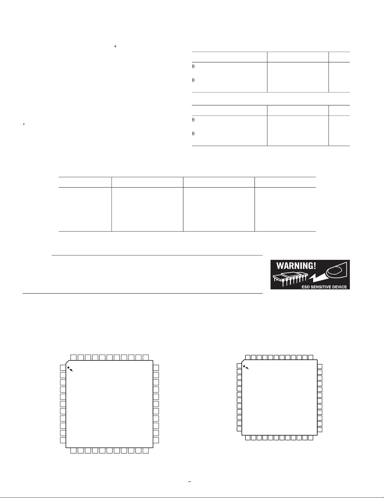
PIN CONFIGURATIONS
44-LEAD MQFP
3
4
5
6
7
1
2
10
11
8
9
40 39 3841
42
4344 36 35 3437
29
30
31
32
33
27
28
25
26
23
24
PIN 1
IDENTIFIER
TOP VIEW
(Not to Scale)
121314 15 16 17 18 192021 22
RESETB
AVDD
AGND
AGND
VOUTL–
VOUTL+
AVDD
AGND
AVDD
VOUTR+
AD1954
CDATA
LRCLK1
SDATA0
BCLK0
LRCKL0
CCLK
MCLK2
MCLK1
MCLK0
DEEMP/SDATA_AUX
MUTE
DVDD
SDATA2
BCLK2
LRCLK2
SDATA1
BCLK1
VOUTR–
AGND
VOUTS+
VOUTS–
CLATCH
DGND
COUT
ODVDD
BCLKOUT
MCLKOUT
DCSOUT
LRCLKOUT
SDATAOUT
ZEROFLAG
FILTCAP
VREF
DGND
48-LEAD LQFP
36
35
34
33
32
31
30
29
28
27
26
25
13 14 15 16 17 18 19 20 21 22 23 24
1
2
3
4
5
6
7
8
9
10
11
12
48 47 46 45 44 39 38 3743 42 41 40
PIN 1
IDENTIFIE
R
TOP VIEW
(Not to Scale)
NC
AGND
VOUTL–
VOUTL+
AVDD
AGND
AVDD
NC
MCLK2
MCLK1
MCLK0
DEEMP/SDATA_AUX
MUTE
DVDD
NC = NO CONNECT
SDATA2
BCLK2
LRCLK2
SDATA1
VOUTR+
VOUTR–
AGND
VOUTS+
AD1954
BCLK1
VOUTS–
DGND
MCLKOUT
COUT
DCSOUT
ODVDD
LRCLKOUT
BCLKOUT
SDATAOUT
ZEROFLAG
FILTERCAP
VREF
NC
DGND
LRCLK1
SDATA0
BCLK0
LRCLK0
CDATA
CCLK
CLATCH
RESETB
AVDD
AGND
NC
Package Characteristics (44-Lead MQFP)
Min
Typ
Max
Unit
JA
(Thermal Resistance—
Junction to Ambient)
JC
(Thermal Resistance—
Junction to Ambient)
Package Characteristics (48-Lead LQFP)
Typ
Max
Unit
JA
(Thermal Resistance—
Junction to Ambient)
JC
(Thermal Resistance—
Junction to Ambient)
Model
Temperature Range
Package Description
Package Option
AD1954YS
–40°C to +105°C
44-Lead MQFP
AD1954YSRL
–40°C to +105°C
44-Lead MQFP
AD1954YST
–40°C to +105°C
48-Lead LQFP
AD1954YSTRL
–40°C to +105°C
48-Lead LQFP
AD1954YSTRL7
–40°C to +105°C
48-Lead LQFP
EVAL-AD1954EB
Evaluation Board

AD1954
PIN FUNCTION DESCRIPTIONS
Pin No.
Pin No.
Input/
Mnemonic
Description
NC
No Connect
MCLK2
IN
Master Clock Input 2 256 f
S
/512 f
S
3
MCLK1
IN
Master Clock Input 1 256 f
S
/512 f
S
3
4
MCLK0
IN
Master Clock Input 0 256 f
S
/512 f
S
4
DEEMP/
IN
Enables 44.1 kHz De-emphasis Filter (Others Available through SPI Control)
Auxiliary Serial Data Input
MUTE
IN
Mute Signal. Initiates volume ramp-down.
DVDD
Digital Supply for DSP Core, 4.5 V to 5.5 V
IN
BCLK2
IN
Bit Clock 2
LRCLK2
IN
Left/Right Clock 2
IN
BCLK1
IN
Bit Clock 1
DGND
Digital Ground
LRCLK1
IN
Left/Right Clock 1
IN
BCLK0
IN
Bit Clock 0
LRCLK0
IN
Left/Right Clock 0
IN
IN
IN
RESETB
IN
Reset Signal, Active Low
AVDD
Analog 5 V Supply
AGND
Analog GND
NC
No Connect
VOUTS–
Negative Sub Analog DAC Output
VOUTS+
Positive Sub Analog DAC Output
AGND
Analog GND
VOUTR–
Negative Left Analog DAC Output
VOUTR+
Positive Left Analog DAC Output
30
AVDD
Analog 5 V Supply
31
AGND
Analog GND
3032AVDD
Analog 5 V Supply
3133VOUTL+
Positive Left Analog DAC Output
3234VOUTL–
Negative Left Analog DAC Output
33
35
AGND
Analog GND
36
NC
No Connect
37
NC
No Connect
34
38
VREF
IN
35
39
FILTCAP
IN
3640ZEROFLAG
Zero Flag Output. High when both left and right channels are 0 for 1024 frames.
37
38
BCLKOUT
Bit Clock Mux Output
3943LRCLKOUT
Left/Right Clock Mux Output
40
44
Digital Supply Pin for Output Drivers, 2.5 V to 5.5 V
41
45
DCSOUT
Data Capture Serial Output for Data Capture Registers. Use in conjunction with
selected LRCLK and BCLK to form a 3-wire output.
42
46
43
MCLKOUT
Master Clock Output 512 f
S
/256 f
S
(Frequency Selected by SPI Register)
48
DGND
Digital Ground
For a complete description of the pins, refer to the Pin Functions section.
–8
AD1954–Typical Performance Characteristics
0
–160
0 202 4 6 8 14 16 18
–20
–80
–120
–40
–60
–100
–140
10 12
kHz
dB
0
–160
0 202 4 6 8 14 16 18
–20
–80
–120
–40
–60
–100
–140
10 12
kHz
dB
Hz
0
–20
20 10k
–10
1k100
–2
–4
–6
–8
–12
–14
–16
–18
50 200 500 5k
dB
2k
3.0
–3.0
–120 0–100 –80 –20
0.5
–1.0
–2.0
0
–0.5
–1.5
–2.5
–60 –40
dBFS
2.5
1.5
2.0
1.0
dB
–2.0
–120 0–100 –80 –20–60
ms
–1.5
–1.0
–0.5
0
0.5
1.0
1.5
2.0
V
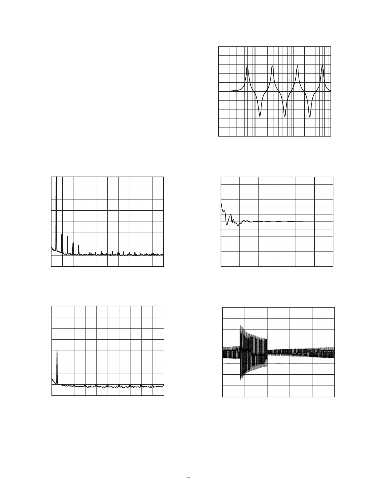
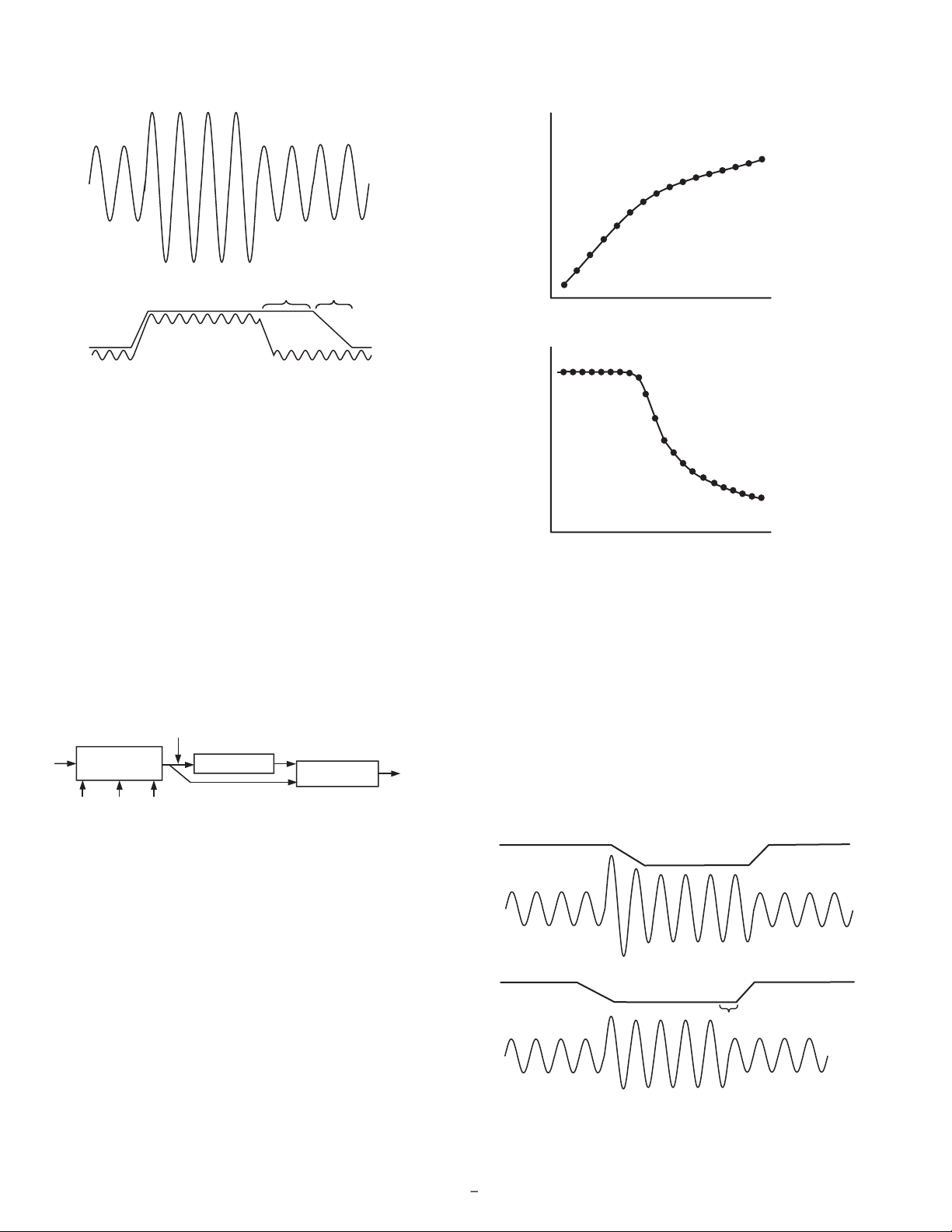
PERFORMANCE PLOTS
The following plots demonstrate the performance achieved on the
with a THD+N of –100 dB, which is dominated by a second
har monic. TPC 2 shows an FFT of a –60 dB sine wave, demon-
strating the lack of low-level artifacts. TPC 3 shows a frequency
response plot with the seven equalization biquads set to an alter-
nating pattern of 6 dB boosts and cuts. TPC 4 shows a linearity
plot, where the measurement was taken with the same equalization
curve used to make TPC 3. When the biquad lters are not in use,
the signal passes through the lters with no quantization effects.
TPC 4 therefore demonstrates that using double-precision math
in the biquad lters has virtually eliminated any quantization
with the attack and recovery characteristics plainly visible. The
rms detector was programmed for normal rms time constants;
the hold/decay feature was not used for this plot.
AD1954
–9
An extensive SPI port allows click-free parameter updates, along
with read-back capability from any point in the algorithm ow.
The AD1954 includes ADI’s patented multibit
DAC architec-
ture. This architecture provides 112 dB SNR and dynamic range
to be used in applications ranging from low-end boom boxes to
high-end professional mixing/editing systems.
The AD1954 also has a digital output that allows it to be used
purely as a DSP. This digital output can also be used to drive an
external DAC to extend the number of channels beyond the three
that are provided on the chip.
This chip can be used with either its default signal processing
program or with a custom user-designed program. Graphical pro-
gramming tools are available from ADI for custom programming.
FEATURES
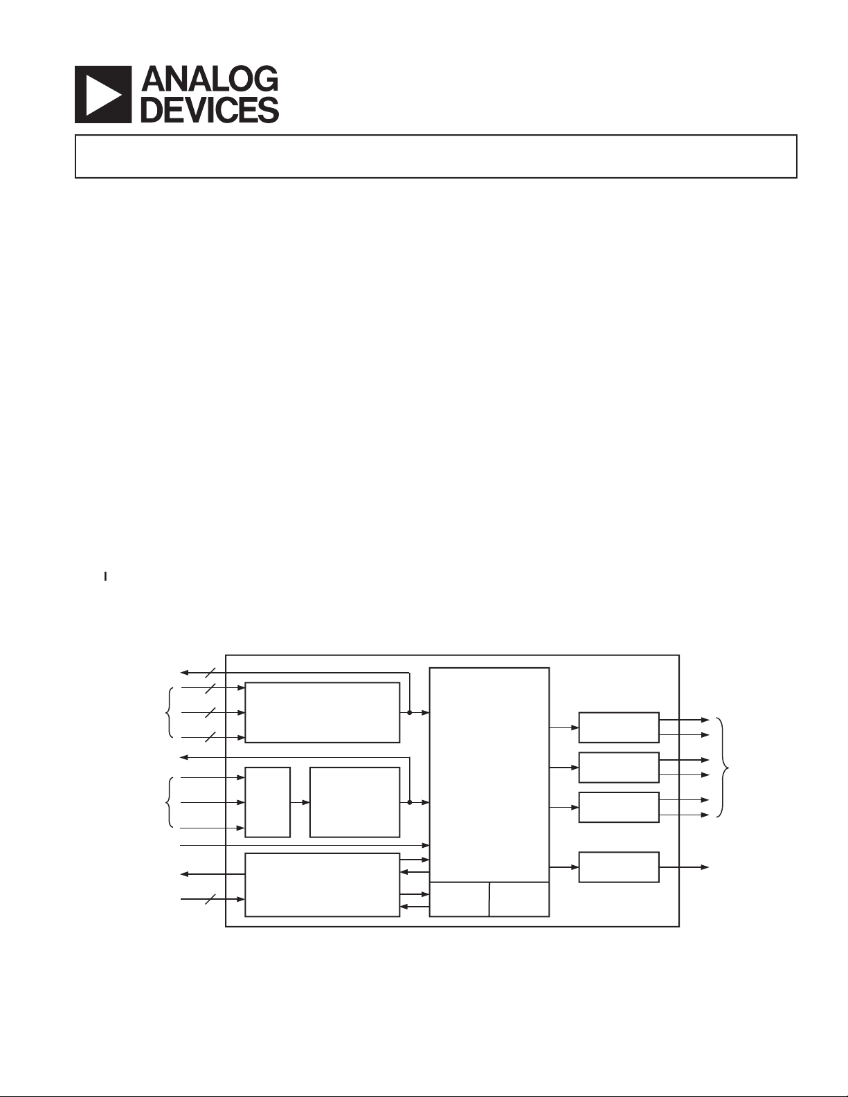
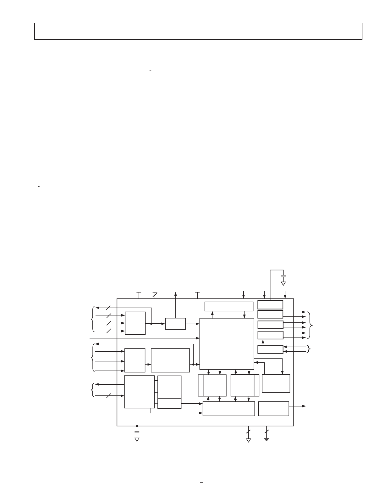
The AD1954 is comprised of a 26-bit DSP (48 bits with double
precision) for interpolation and audio processing, three multibit
modulators, and analog output drive circuitry. Other features
include an on-chip parameter RAM that uses a safe-upload feature
for transparent and simultaneous updates of lter coef cients and
digital de-emphasis lters. Also, on-chip input selectors allow up
to three sources of serial data and master clock to be selected.
The 3-channel con guration is especially useful for 2.1 playback
systems that include two satellite speakers and a subwoofer.
The default program allows for independent equalization and
compression/limiting for the satellite and subwoofer outputs.
Figure 1 shows the block diagram of the device.
The AD1954 contains a program RAM that boots from an internal
program ROM on power-up. Signal processing parameters are
stored in a 256-location parameter RAM, which is initialized on
power-up by an internal boot ROM. New values are written to
the parameter RAM using the SPI port. The values stored in the
parameter RAM control the IIR equalization lters, the dual-
band compressor/limiter, the delay values, and the settings of the
stereo spreading algorithm.
The AD1954 has a very sophisticated SPI port that supports
complete read/write capability of both the program and the para-
meter RAM. Two control registers are also provided to control
the chip serial modes and various other optional features. Hand-
shaking is also included for ease of memory uploads/downloads.
The AD1954 contains four independent data capture circuits,
which can be programmed to tap the signal ow of the processor
can be accessed either through a separate serial out pin (i.e., that
can be connected to an external DAC or DSP) or by reading from
the data capture SPI registers. This allows the basic functionality
of the AD1954 to be easily extended.
The processor core in the AD1954 has been designed from the
ground up for straightforward coding of sophisticated compres-
sion/limiting algorithms. The AD1954 contains two independent
compressor/limiters with rms based amplitude detection and
curve that is loaded by the user into a look-up table that resides
in the parameter RAM. The compressor also features look-ahead
compression that prevents compressor overshoots.
continued from page 1
)
3:1
AUDIO
DATA
MUX
1
3
3
SPI PORT
3:1
MCLK
MUX
1
DAC – L
COEFFICIENT
RO
M
64 22
26 22
DSP CORE
DATA FORMAT
:
3.23 (SINGLE PRECISION)
3.45 (DOUBLE PRECISION)
3
3
ANALOG
OUTPUTS
MASTER
CLOCK I/O
GROUP
DCSOUT
SPI I/O
GROUP
3
SERIAL
IN
1
DATA MEMORY, 512 26
CONTROL
REGISTERS
TRAP REG.
(I2S, SPI)
SAFELOAD
REGISTERS
PROGRAM
RAM
512 35
PARAMETER
RAM
256 22
BOOT ROM
BOOT ROM
MEMORY CONTROLLERS
DAC – R
DAC – SW
2
BIAS
ANALOG
BIAS GR
OUP
RESETB
MUTE
DE-EMPHASIS
ZEROFLAG
NOTES
1
CONTROLLED THROUGH SPI CONTROL REGISTERS.
2
DAC DOES NOT USE DIGITAL INTERPOLATION.
SERIAL DATA I/O
GROUP
DCSOUT TRAP
AUX SERIAL
DATA
INPUT
MCLK
GENERATO
R
1
(256 fS/512 fS IN)
256
f
S
/512
f
S
OUT
VOLTAGE
REFERENCE
VREF
DV
DD AVDD ODVDD
3
FILTCAP
AGND DGND
3 2

AD1954
–10
The AD1954 has a very exible serial data input port, which
chips, AES/EBU receivers, and sample rate converters. The
AD1954 can be con gured in left-justi ed, I
2
DSP serial port compatible modes. It can support 16 bits, 20 bits,
in MSB rst, twos complement format. The part can also be set
up in a 4-channel serial input mode by simultaneously using the
serial input mux and the auxiliary serial input.
The AD1954 operates from a single 5 V power supply. It is fabri-
cated on a single monolithic integrated circuit and is housed in a
44-lead MQFP or 48-lead LQFP package for operation over the
temperature range –40°C to +105°C.
PIN FUNCTIONS
All input pins have a logic threshold compatible with TTL input
levels and can therefore be used in systems with 3.3 V logic. All
digital output levels are controlled by the ODVDD pin, which
may range from 2.7 V to 5.5 V, for compatibility with a wide
range of external devices. (See Pin Function Descriptions table.)
—Serial Data Inputs
writing to Bits 7 and 6 in Control Register 2. Default is 00, which
selects SDATA0. The serial format is selected by writing to Bits 3–0
of Control Register 0. See SPI Read/Write Data Formats section
for recommendations on how to change input sources without
causing a click or pop noise.
LRCLK0, LRCLK1, LRCLK2
—Left/Right Clocks for Framing the
Input Data
The active LRCLK input is selected by writing to Bits 7 and 6
in Control Register 2. The default is 00, which selects LRCLK0.
The interpretation of the LRCLK changes according to the serial
mode, set by writing to Control Register 0.
BCLK0, BCLK1, BCLK2
—Serial Bit Clocks for Clocking in the
The active BCLK input is selected by writing to Bits 7 and 6 in
interpretation of BCLK changes according to the serial mode,
which is set by writing to Control Register 0.
LRCLKOUT, BCLKOUT, SDATAOUT
—Output of Mux that
These pins may be used to send the selected serial input signals
to other external devices. This output pin is enabled by writing a
MCLK0, MCLK1, MCLK2
—Master Clock Inputs
Active input selected by writing to Bits 5 and 4 of Control Regis-
ter 2. The default is 00, which selects MCLK0. The master clock
frequency must be either 256
f
S
or 512
f
S
, where f
S
is the input
sampling rate. The master clock frequency is programmed by
writing to Bit 2 of Control Register 2. The default is 0 (512
S
).
how to change clock sources without causing an audio click or pop.
Note that since the default MCLK source pin is MCLK0, there
must be a clock signal present on this pin on power-up so that
the AD1954 can complete its initialization routine.
MCLKOUT
—Master Clock Output
The master clock output pin may be programmed to produce
either 256
S
, 512
S
, or a copy of the selected MCLK input
pin. This pin is programmed by writing to Bits 1 and 0 of Control
Register 2. The default is 00, which disables the MCLKO pin.
—Serial Data In for the SPI Control Port
—Serial Data Output
This is used for reading back registers and memory locations. It
is three-stated when an SPI read is not active. See SPI Port section
for more information on SPI port timing.
—SPI Bit Rate Clock
This pin either may run continuously or be gated off in between
—SPI Latch Signal
It must go low at the beginning of an SPI transaction and high at the
end of a transaction. Each SPI transaction may take a different
number of CCLKs to complete, depending on the address and
read/write bit that are sent at the beginning of the SPI transaction.
Detailed SPI timing information is given in SPI Port section.
RESETB
—Active Low Reset Signal
After RESETB goes high, the AD1954 goes through an initial-
ization sequence where the program and parameter RAMs are
initialized with the contents of the on-board boot ROMs. All
initialization is complete after 1024 MCLK cycles. Since the
MCLK IN FREQ SELECT (Bit 2 in Control Register 2) defaults
to 512
S
at power-up, this initialization will proceed at the
external MCLK rate and will take 1024 MCLK cycles to com-
plete, regardless of the absolute frequency of the external MCLK.
New values should not be written to the SPI port until the initial-
ization is complete.
ZEROFLAG
—Zero-Input Indicator
This pin will go high if both serial inputs have been inactive (zero
data) for 1024 LRCLK cycles. This pin may be used to drive an
external mute FET for reduced noise during digital silence. This
pin also functions as a test out pin, controlled by the test register
end user, one may be of some use. If the Test Register is pro-
grammed with the number 7 (decimal), the ZEROFLAG output
will be switched to the output of the internal pseudo-random noise
generator. This noise generator operates at a bit rate of 128
f
S
used to generate white noise (or, with appropriate ltering, pink
noise) to be used as a test signal for measuring speakers or room

AD1954
DCSOUT
—Data Capture Serial Out
This pin will output the DSP’s internal signals, which can be used
by external DACs or other signal processing devices. The signals
that are captured and output on the DCSOUT pin are controlled
by writing program counter trap numbers to SPI Addresses 263
nal program counter contents are equal to the trap values written
to the SPI port, the selected DSP register is transferred to the
DCSOUT parallel-to-serial registers and shifted out on the
DCSOUT pin. Table XX shows the program counter trap values
nal points of the algorithm ow.
The DCSOUT pin is meant to be used in conjunction with the
LRCLK and BCLK signals that are provided to the serial input
port. The format of DCSOUT is the same as the format used
for the serial port. In other words, if the serial port is running in
I
3-wire I
2
The DCSOUT pin can be used for a variety of purposes. If the
DCSOUT pin is used to drive another external DAC, then a
4.1 system is possible using a new program downloaded into the
program RAM.
DEEMP/SDATA_AUX
—De-emphasis Input Pin/Auxiliary Serial
Data Input
In de-emphasis mode, if this pin is asserted high, then a digital
de-emphasis lter will be inserted into the signal ow. The
de-emphasis curve is valid only for a sample rate of 44.1 kHz;
curves for 32 kHz and 48 kHz may be programmed using the
data input. This function is set by writing a 1 to Bit 11 of Control
Register 1. The same clocks are used for this serial input as are
used for the SDATA0, SDATA1, and SDATA2 signals. This serial
input can only be used in the signal processing ow when using
Analog Devices’ custom programming tools; see the Graphical
still available while this pin is used as a serial input but only
through SPI control.
MUTE
—Mute Output Signal
When this pin is asserted high, a ramp sequence is started, which
gradually reduces the volume to zero. When de-asserted, the volume
ramps from zero back to the original volume setting. The ramp
speed is timed so that it takes 10 ms to reach 0 volume when starting
from the default 0 dB volume setting.
VOUTL+, VOUTL2
—Left Channel Differential Analog Outputs
Full-scale outputs correspond to 1 Vrms on each output pin or
The full-scale swing scales directly with VREF. These outputs are
capable of driving a load of >5 k
, with a maximum peak current
of 1 mA from each pin. An external third order lter is recom-
mended for ltering out-of-band noise.
VOUTR+, VOUTR2
—Right Channel Differential Outputs
left channel
VOUTL+, VOUTL–.
VOUTS+, VOUTS2
—Subchannel Differential Outputs
These outputs are designed to drive loads of 10 k
or greater,
with a peak current capability of 250 µA. This output does not
use digital interpolation, since it is intended for low frequency
VREF
—Analog Reference Voltage Input
The nominal VREF input voltage is 2.5 V; the analog gain scales
directly with the voltage on this pin. When using the AD1954 to
drive a power ampli er, it is recommended that the VREF voltage
be derived by dividing down and heavily ltering the supply to the
power ampli er. This provides a bene t if the compressor/limiter
in the AD1954 is used to prevent ampli er clipping. In this case, if
the DAC output voltage is scaled to the ampli er power supply, a
xed compressor threshold can be used to protect an ampli er
whose supply may vary over a wide range. Any ac signal on this
pin will cause distortion, and therefore, a large decoupling capaci-
tor may be necessary to ensure that the voltage on VREF is clean.
The input impedance of VREF is greater than 1 M
FILTCAP
—Filter Capacitor Point
This pin is used to reduce the noise on an internal biasing point
in order to provide the highest performance. It may not be neces-
sary to connect this pin, depending on the quality of the layout
DVDD
—Digital VDD for Core
—Digital VDD for All Digital Outputs
Variable from 2.7 V to 5.5 V.
DGND (2)
—Digital Ground
AVDD (3)
—Analog VDD
Bypass capacitors should be placed close to the pins and connected
directly to the analog ground plane.
AGND (3)
—Analog Ground
For best performance, separate nonoverlapping analog and digital
ground planes should be used.

AD1954
Figure 2 shows the signal processing ow diagram of the AD1954.
The AD1954 is designed to provide all the signal processing
functions commonly used in 2.0 or 2.1 playback systems. A seven-
biquad equalizer operates on the stereo input signal. The output of
this equalizer is fed to a two-biquad crossover lter for the main
channels, and the mono sum of the left and right equalizer outputs
is fed to a three-biquad crossover lter for the subchannel. Each
of the three channels has independent delay compensation. There
on the left/right outputs and one operating on the subwoofer chan-
nel. The subwoofer output may be blended back into the left/right
outputs for 2.0 playback systems. In this con guration, the two
independent compressor/limiters provide two-band compression,
which signi cantly improves the sound quality of compressed
Most of the signal processing functions are coded using full 48-bit
double-precision arithmetic. The input word length is 24 bits, with
two extra headroom bits added in the processor to allow internal
gains up to 12 dB without clipping (additional gains can be
lter section).
A graphical user interface (GUI) is available for evaluation of
the AD1954 (Figure 3). This GUI controls all of the functions of
the chip in a very straightforward and user friendly interface. No
code needs to be written to use the GUI to control the chip. For
more information on AD1954 software tools, send an e-mail to
Each section of this ow diagram will be explained in detail on
the following pages.
Numeric Formats
It is common in DSP systems to use a standardized method of
specifying numeric formats. To better comprehend issues relating to
precision and over ow, it is helpful to think in terms of fractional
twos complement number systems. Fractional number systems
the left of the decimal point, and B is the number of bits to the
right of the decimal point. In a twos complement system, there is
in a twos complement 1.23 system, the legal signal range is
–1.0 to +(1.0 – 1 LSB).
The AD1954 uses two different numeric formats: one for the
coef cient values (stored in the parameter RAM) and one for the
signal data values. The coef cient format is as follows:
Range: –2.0 to +(2.0 – 1 LSB)
Examples:
This format is used because standard biquad lters require
coef cients that range between +2.0 and –2.0. It also allows gain
to be inserted at various places in the signal path.
Internal DSP Signal Data Format
Input Data Format: 1.23
This is sign extended when written to the data memory of the
AD1954.
Internal DSP Signal Data Format: 3.23
Range: –4.0 to +(4.0 – 1 LSB)
Examples:
The sign extension between the serial port and the DSP core
clipping. Gains greater than 12 dB can be accommodated by
scaling the input down in the rst biquad lter and scaling the
signal back up at the end of the biquad lter section.
A digital clipper circuit is used between the output of the DSP
core and the input to the DAC
modulators to prevent over-
loading the DAC circuitry (see Figure 4). Note that there is a gain
factor of 0.75 used in the DAC interpolation lters, and therefore
signal values of up to 1/0.75 will pass through the DSP without
clipping. Since the DAC is designed to produce an analog output
of 2 V rms (differential) with a 0 dB digital input, signals between
HPF/
DEEMPH
HPF/
DEEMPH
IN
RIGHT
IN
LEFT
VOLUME
VOLUME
PHAT STEREO
DELAY
(0
ms–3.7ms)
DELAY
(0
ms–3.7ms)
DELAY
(0
ms–2.3ms)
DELAY
(0
ms–2.3ms)
8
INTERPOLATION
DAC
OUT
LEFT
8
INTERPOLATION
DAC
OUT
RIGHT
VOLUME
1 BIQUAD
FILTER
DELAY
(0
ms–3.7ms)
MONO DAC
L/R REINJECTION
LEVEL
SUBWOOFER
OUTPUT
SUB DYNAMICS PROCESSO
R
SUB CHANNEL
L/R MIX
EQ AND CROSSOVER FILTERS
L/R DYNAMICS PROCESSO
R
LEVEL DETECT,
LOOK-UP TABL
E
LEVEL DETECT,
LOOK-UP TABL
E
7 BIQUAD
FILTERS
7 BIQUAD
FILTERS
CROSSOVER
(2 FILTERS)
CROSSOVER
(2 FILTERS)
CROSSOVER
(3 FILTERS)

AD1954
–13
outputs and result in slightly degraded analog performance. This
extra analog range is necessary in order to pass 0 dBFS square
waves through the system, since these square waves cause over-
shoots in the interpolation lters, which would otherwise brie y
clip the digital DAC circuitry.
A separate digital clipper circuit is used in the DSP core to ensure
that any accumulator values that exceed the numeric 3.23 format
range are clipped when taken from the accumulator.
High-Pass Filter
The high-pass lter is a rst order double-precision design. The pur-
pose of the high-pass lter is to remove digital dc from the input. If
this dc were allowed to pass, the detectors used in the compres sor/
limiter would give an incorrect reading for low signal levels. The
high-pass lter is controlled by a single parameter (alpha_HPF),
which is programmed by writing to SPI location 180 in 2.20 twos
complement format. The following equation can be used to calcu-
late the parameter alpha_HPF from the –3 dB point of the lter:
Alpha_HPF – EXP
p HPF_Cutoff
f
S
=
× ×
1.0
–2.0
where
is the exponential operator,
HPF_cutoff
is the high-
pass cutoff in Hz, and
fS is the audio sampling rate. The default
is the audio sampling rate. The default
value for the –3 dB cutoff of the high-pass lter is 2.75 Hz at a
sampling rate of 44.1 kHz.
Biquad Filters
Each of the two input channels has seven second order biquad
sections in the signal path. In addition, the left and right channels
have two additional biquad lters that may be used either as
crossover lters or as additional equalization lters. The subchan-
nel has three additional biquad lters that are also to be used
rst seven biquads would be used for speaker equalization and/or
tone controls, and the remaining lters would be programmed to
function as crossover lters. Note that there is a common equal-
ization section used for both the main and sub channels, followed
by the crossover lters. This arrangement prevents any interaction
from occurring between the crossover lters and the equalization
lters. One section of the biquad IIR lter is shown in Figure 5.
SIGNAL PROCESSING
(3.23 FORMAT)
SERIAL PORT
DAC INTERPOLATION
FILTERS (3.23 FORMAT
)
DIGITAL -
MODULATORS
(1.23 FORMAT
)
DIGITAL
CLIPPER
DATA IN
2-BIT SIGN EXTENTION
0.75
1.23
3.23

AD1954
b0
IN
OUT
b1
b2
a1
a2
Z
–1
Z
–1
Z
–1
Z
–1
This section implements the transfer function:
H Z
b b Z b
Z
a Z – a
Z
( )
=
+ × + ×
( )
− × ×
( )
0 1
1 1
–1 –2
–1 –2
2
2
The coef cients a1, a2, b0, b1, and b2 are all in twos comple-
ment 2.20 format with a range from –2 to +2 (minus 1 LSB).
The negative sign on the a1 and a2 coef cients is the result of
terms. Some digital lter packages automatically produce the
correct a1 and a2 coef cients for the topology of Figure 5, while
others assume a denominator of the form 1 + a1 × Z
–1
+ a2
–1
terms for proper operation.
The biquad structure shown in Figure 5 is coded using double-
precision math to avoid limit cycles from occurring when low
frequency lters are used. The coef cients are programmed
by writing to the appropriate location in the parameter RAM,
through the SPI port (see Table VI). There are two possible sce-
narios for controlling the biquad lters:
Dynamic Adjustment (e.g., Bass/Treble Control or Parametric
Equalizer).
When using dynamic lter adjustment, it is highly recom-
mended that the user employ the safeload mechanism to avoid
temporary instability when the lters are dynamically updated.
This could occur if some, but not all, of the coef cients were
updated to new values when the DSP calculates the lter
output. The operation of the safeload registers is detailed in
the Options for Parameter Updates section.
If many of the biquad lters need to be initialized after power-
up (e.g., to implement a static speaker correction curve), the
recommended procedure is to set the processor shutdown bit,
wait for the volume to ramp down (about 20 ms), and then
write directly to the parameter RAM in burst mode. After the
RAM is loaded, the shutdown bit can be de-asserted, causing
the volume to ramp back up to the initial value. This entire proce-
dure is click-free and faster than using the safeload mechanism.
The data paths of the AD1954 contain an extra two bits on top of
the 24 bits that are input to the serial port. This allows up to 12 dB
of boost without clipping. However, it is important to remember
that it is possible to design a lter that has less than 12 dB of gain
of one or more intermediate biquad lter sections. For this reason,
it is important to cascade the lter sections in the correct order,
putting the sections with the largest peak gains at the end of the
chain rather than at the beginning. This is standard practice when
coding IIR lters and is covered in basic books on DSP coding.
If gains larger than 12 dB cannot be avoided, then the coef cients
b0 through b2 of the rst biquad section may be scaled down
to t the signal into the 12 dB maximum signal range and then
scaled back up at the end of the lter chain.
Volume
Three separate SPI registers are used to control the volume—one
each for the left, right, and sub channels. These registers are
special in that they include automatic digital ramp circuitry for
clickless volume adjustment. The volume control word is in 2.20
format and therefore gains from +2.0 to –2.0 are possible. The
default value is 1.0. It takes 1024 audio frames to adjust the vol-
ume from 2.0 down to 0; in the normal case where the maximum
volume is set to 1.0, it will take 512 audio frames for this ramp to
reach zero. Note that a mute command is the same as setting the
volume to zero, except that when the part is unmuted, the vol-
ume returns to its original value.
These volume ramp times assume that the AD1954 is set for
the fast volume ramp speed. If the slow setting is selected, it will
take 8192 audio frames to reach zero from a setting of 2.0. Cor-
respondingly, it will take 4096 frames to reach 0 volume from the
normal setting of 1.0.
The volume blocks are placed after the biquad lter sections to
maximize the level of the signal that is passed through the lter
sections. In a typical situation, the nominal volume setting might
be –15 dB, allowing a substantial increase in volume when the user
increases the volume. The AD1954 was designed with an analog
dynamic range of >112 dB, so that in the typical situation with
the volume set to –15 dB, the signal-to-noise ratio at the output
will still exceed 97 dB. Greater output dynamic ranges are pos-
sible if the compressor/limiter is used, since the post-compression
gain parameter can boost the signal back up to a higher level. In
this case, the compressor will prevent the output from clipping
when the volume is turned up and the input signal is large.
The image enhancement processing is based on ADI’s patented
Phat Stereo algorithm. The block diagram is shown in Figure 6.
1kHz
FIRST ORDER LPF
LEVEL
LEFT IN
RIGHT IN
LEFT OUT
RIGHT OUT
+
+
–
–
–
The algorithm works by increasing the phase shift for low frequency
signals that are panned left or right in the stereo mix. Since the ear
is responsive to interaural phase shifts below 1 kHz, this increase in
phase shifts results in a widening of the stereo image. Note that
signals panned to the center are not processed, resulting in a more
natural sound. There are two parameters that control the Phat
of-phase information is added to the left and right channels, and
the cutoff frequency of the rst order low-pass lter, which deter-
mines the frequency range of the added out-of-phase signals. For
best results, the cutoff frequency should be in the range of 500 Hz
to 2 kHz. These parameters are controlled by altering the param-
eter RAM locations that store the parameters spread_level and
that multiplies the processed left-right signal before it is added to or
subtracted from the main channels. The parameter alpha_spread

AD1954
–15
is related to the cutoff frequency of the rst order low-pass lter
by the equation:
Alpha_Spread – EXP
p Spread_Freq
f
S
=
× ×
1.0
–2.0
where
EXP
is the exponential operator,
Spread_Freq
is the low-pass
cutoff in Hz, and
fS is the audio sampling rate.
is the audio sampling rate.
Note that the stereo spreading algorithm assumes that frequencies
below 1 kHz are present in the main satellite speakers. In some
systems, the crossover frequency between the satellite and sub-
woofer speakers is quite high (>500 Hz). In such a case, the stereo
spreading algorithm will not be effective, since the frequencies
that contribute to the spreading effect will come mostly from the
subwoofer, which is a mono source.
Delay
Each of the three DAC channels has a delay block that allows the
user to introduce a delay of up to 165 audio samples. The delay
values are programmed by entering the delay (in samples) into
the appropriate location of the parameter RAM. With a 44.1 kHz
sample rate, a delay of 165 samples corresponds to a time delay
of 3.74 ms. Since sound travels at approximately 1 foot/ms, this
can be used to compensate for speaker placements that are off by
An additional 100 samples of delay are used in the look-ahead
portion of the compressor/limiter but only for the main two chan-
nels. This can be used to increase the total delay for the left and
right channels to 265 samples or 6 ms at 44.1 kHz.
Main Compressor/Limiter
The compressor used in the AD1954 is quite sophisticated and is
comparable in many ways to the professional compressor/limiters
used in the professional audio and broadcast elds. It uses rms/
peak detection with adjustable attack/hold/release, look-ahead
compression, and table-based entry of the input/output curve for
complete exibility.
The AD1954 uses two compressor/limiters: one in the subwoofer
DAC and one in the main left/right DAC. It is well known that
having independent compressors operating over different fre-
quency ranges results in a superior perceived sound. With a
single-band compressor, loud bass information will modulate the
gain of the entire audio signal, resulting in suboptimal maximum
perceived loudness as well as gain pumping or modulation effects.
With independent compressors operating separately on the low
AD1954 is being operated in two-channel mode, an extra path is
main channel. This maintains the advantage of using a two-band
compressor, even in a 2.0 system con guration.
Figure 7 shows the traditional basic analog compressor/limiter.
It uses a voltage controlled ampli er to adjust gain and a feed-
forward detector path using an rms detector with adjustable time
constants, followed by a nonlinear circuit, to implement the
desired input/output relationship. A simple compressor will have
compression above the threshold is called the compression ratio
example, if the input to a 2:1 compressor is increased by 2 dB,
the output will rise by 1 dB for signals above the threshold.
A single hard threshold results in more audible behavior than a
so-called soft-knee compressor, where the compression is in-
troduced more gradually. In an analog compressor, the soft-knee
characteristic is usually made by using diodes in their exponential
turn-on region.
FILTER
RMS DETECTOR
WITH DB OUT
COMPRESSION
CURVE
NONLINEAR
CIRCUITS
VCA WITH EXP
CONTROL
THRESHOLD
SLOPE
OUT
The best analog compressors use rms detection as the signal
tive to the phase of the harmonics in a complex signal are rms
detectors. The ear also bases its loudness judgment on the overall
signal power and therefore using an rms detector results in the
best audible performance. Compressors that are based on peak
detection, while good for preventing clipping, are generally quite
poor for audible performance.
RMS detectors have a certain time constant that determines how
rapidly they can respond to transient signals. There is always a
trade-off between speed of response and distortion. Figure 8
shows this trade-off.
INPUT WAVEFORM
COMPRESSOR ENVELOPE—
FAST TIME CONSTANT
COMPRESSOR ENVELOPE—
SLOW TIME CONSTANT
In the case of a fast-responding rms detector, the detector envelope
will have a signal component in addition to the desired dc com-
ponent. This signal component (which, for an rms detector, is
when multiplied by this detector signal.
The AD1954 uses a modi ed rms algorithm to improve the relation-
ship between acquisition time and distortion. It uses a peak-riding
circuit together with a hold circuit to modify the rms signal, as
shown in Figure 9. This gure shows two envelopes. One has the
harmonic distortion, as seen in the previous gure, and the other,
atter envelope is the one produced by the AD1954.
AD1954
–16
INPUT WAVEFORM
HOLD TIME, SPI-
PROGRAMMABLE
RELEASE TIME, SPI-
PROGRAMMABLE
Using this idea of a modi ed rms algorithm, the true rms value
is still obtained for all but the lowest frequency signals, while the
distortion due to rms ripple is reduced. It also allows the user to
set the hold and release times of the compressor independently.
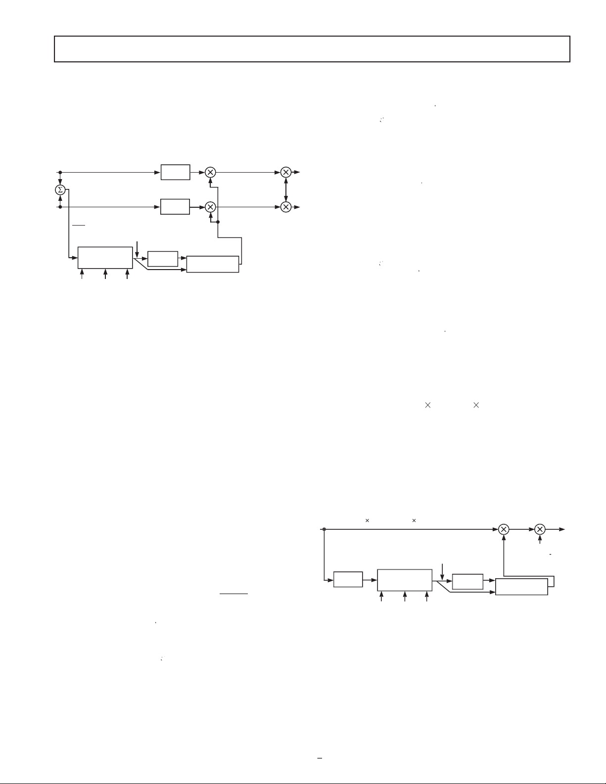
The detector path of the AD1954 is shown in Figure 10. The rms
detector is controlled by three parameters stored in the parameter
RAMs: the rms time constant, the hold time, and the release rate.
The log output of the rms detector is applied to a look-up table
with interpolation. The higher bits of the rms output form an
offset into this table, and the lower bits are used to interpolate
between the table entries to form a high-precision gain word. The
look-up table resides in the parameter RAM and is loaded by
the user to give the desired curve. The look-up table contains 33
data locations, and the LSB of the address into the look-up table
corresponds to a 3 dB change in the amplitude of the detector
signal. This gives the user the ability to program an input/output
curve over a 99 dB range. For the main compressor, the table
resides in Locations 110 to 142 in the SPI parameter RAM.
LOOK-UP TABLE
LINEAR
INTERPOLATION
MODIFIED RMS
DETECTOR WITH
LOG OUTPUT
OUTPUT TO
GAIN STAGE
HIGH BITS (1LSB = 3dB)
LOW BITS
TIME
CONSTANT
HOLD
RELEASE
the rms value of a sine wave and that of a square wave. If a full-
scale square wave is applied to the AD1954, the rms value of this
signal will be 3 dB higher than the rms value of a 0 dBFS sine
wave. Therefore, the table ranges from +9 dB (Location 142) to
–87 dB (Location 110).
The entries in the table are linear gain words in 2.20 format.
Figure 11 shows an example of the table entries for a simple
INPUT LEVEL – 3dB/TABLE ENTRY
OUTPUT LEVEL – dB
INPUT LEVEL – 3dB/TABLE ENTRY
LINEAR GAIN
DESIRED
COMPRESSION
CURVE
Note that the maximum gain that can be entered in the table is
sion curve may be shifted upward by using the post-compression
gain block following the compressor/limiter.
The AD1954 compressor/limiter also includes a look-ahead com-
pression feature. The idea behind look-ahead compression is to
prevent compressor overshoots by applying some digital delay to
the signal before the gain-control multiplier but not to the detec-
tor path. In this way, the detector can acquire the new amplitude
of the input signal before the signal actually reaches the multiplier.
A comparison of a tone burst fed to a conventional compressor
versus a look-ahead compressor is shown in Figure 12.
CONVENTIONAL COMPRESSOR GAIN
LOOK-AHEAD COMPRESSOR GAIN
HOLD TIME
AD1954
In the look-ahead compressor, the gain has already been reduced
by the time that the tone-burst signal arrives at the multiplier input.
Note that when using a look-ahead compressor, it is important to
set the detector hold time to a value that is at least the same as
the look-ahead delay time or the compressor release will start too
soon, resulting in an expanded tail of a tone-burst signal. The
complete ow of the left/right dynamics processor is shown in
Figure 13.
LOOK-UP
TABLE
LINEAR
INTERPOLATION
MODIFIED RMS
DETECTOR WITH
LOG OUTPUT
HIGH BITS (1LSB = 3dB)
LOW BITS
TIME
CONSTANT
HOLD
RELEASE
DELAY
DELAY
SPI-PROGRAMMABLE
LOOK-AHEAD DELAY
POSTCOMPRESSION
GAIN, SPI-
PROGRAMMABLE
UP TO 30dB
2
(L+R)
The detector path works from the sum of the left and right channels
counts on the fact that the main instruments in any stereo mix are
seldom recorded deliberately out of phase, especially in the lower
frequencies that tend to dominate the energy spectrum of real music.
The compressor is followed by a block known as post-compression
gain. Most compressors are used to reduce the dynamic range
of music by lowering the gain during loud signal passages. This
results in an overall loss of volume. This loss can be made up by
introducing gain after the compressor. In the AD1954, the coef-
cient format used is 2.20, which has a maximum oating-point
representation of slightly less than 2.0. This means that the maxi-
mum gain that can be achieved in a single instruction is 6 dB. To
get more gain, the program in the AD1954 uses a cascade of ve
multipliers to achieve up to 30 dB of post-compression gain.
To program the compressor/limiter, the following formulas may
be used to determine the 22-bit numbers (in 2.20 format) to be
entered into the parameter RAM.
RMS Time Constant
This can be best expressed by entering the time constant in terms
of dB/sec raw release rate (without the peak-riding circuit). The
change in amplitude of the input sine wave.
rms_tconst_parameter –
_
=
×
( )
1.0 10
.
release rate
f
S
10 0
where
rms_tconst_parameter
= the fractional number to enter into
the SPI RAM (after converting to 22-bit 2.20 format), and the
release_rate = the
release rate
of the raw rms detector in dB/sec.
This must be negative, and
fS = the audio sample rate.
= the audio sample rate.
RMS Hold Time
rms_hold_time_parameter int hold_time= ×
( )
f
S
Where
rms_holdtime_parameter
= the integer number to enter into
the SPI RAM,
fS = the audio sample rate,
= the audio sample rate,
hold_time
= the abso-
lute time to wait before starting the release ramp-down of the
detector output, and
int
RMS Release Rate
rms_decay_parameter int rms_decay /=
( )
0.137
where
rms_decay_parameter
= the decimal integer number to enter
into the SPI RAM,
rms_decay
= the decay rate in dB/sec, and
int
Look-Ahead Delay
lookahead_delay_parameter lookahead_delay f= ×
S
where
lookahead_delay
= the predictive compressor delay in
fS = the audio sample rate, and the maximum
= the audio sample rate, and the maximum
lookahead_delay_parameter
value is 100.
Postcompression Gain
post_compression_gain_parameter
post_compression_gain_linear
=
( )
∧
1/5
where
post_compression_gain_linear
is the linear post-compression
gain and ^ = the raise to the power.
The subwoofer compressor/limiter differs from the left/right
compressor in the following ways:
The subwoofer compressor operates on a weighted sum of the
left and right inputs (aa
Left + bb
Right), where aa and
bb are both programmable.
The detector input has a biquad lter in series with the input
in order to implement frequency-dependent compression
thresholds.
3.
There is no predictive compression since presumably the input
signals are ltered to pass only low frequencies and therefore
transient overshoots are not a problem.
The subwoofer compressor signal ow is shown in Figure 14.
TABL
INTERPOLATION
S
S
CONSTANT
IN
_SUB = k1
LEFT_IN + K2
RIGHT_IN
GAIN, SPI

AD1954
–18
The biquad lter before the detector can be used to implement a
frequency-dependent compression threshold. For example, assume
that the overload point of the woofer is very frequency depen-
dent. In this case, one would have to set the compressor threshold
to a value that corresponded to the most sensitive overload fre-
quency of the woofer. If the input signal happened to be mostly
in a frequency range where the woofer was not so sensitive to
overload, then the compressor would be too pessimistic and the
volume of the woofer would be reduced. If, on the other hand,
the biquad lter were designed to follow the woofer excursion
curve of the speaker, then the volume of the woofer could be
maximized under all conditions. This is illustrated in Figure 15.
20Hz 200Hz
FREQUENCY
WOOFER EXCURSION
BIQUAD RESPONSE
20Hz
FREQUENCY
200Hz
When using a lter in front of the detector, a confusing side effect
occurs. If one measures the frequency response by using a swept
sine wave with an amplitude large enough to be above the com-
pressor threshold, the resulting frequency response will not look
at. However, this is not real in the sense that, as the sine wave is
swept through the system, the gain is being slowly modulated up
the detector. If one measures the response using a pink noise gen-
erator, the result will look much better, since the detector will settle
on only one gain value. The perceptual effect of the swept sine wave
test is not at all what would be predicted by simply looking at the
frequency response curve; it is only the signal path lters that will
path lters.
De-emphasis Filtering
The standard for encoding CDs allows the use of a pre- emphasis
curve during encoding, which must be compensated for by a
de-emphasis cur ve during playback. The de - emphasis curve
is de ned as a rst order shelving lter with a single pole at
50 µs)) followed by a single zero at (1/(2
15 µs)).
This cur ve may be accurately modeled using a rst order digital
lter. This lter is included in the AD1954; it is not part of the
bank of biquad lters and so does not take away from the num-
ber of available lters.
incoming sampling rate. However, when the de-emphasis lter is
implemented digitally, the response will scale with the sampling
rate unless the lter coef cients are altered to suit each possible
input sampling rate. For this reason, the AD1954 includes three
separate de-emphasis curves: one each for sampling rates of
32 kHz, 44.1 kHz, and 48 kHz. These curves are selected by
writing to Bits 5 and 4 of Control Register 1 over the SPI port.
Alternatively, the 44.1 kHz curve can be called upon using the
DEEMP/SDATA_AUX pin. This pin is included for compatibility
with CD decoder chips that have a de-emphasis output pin.
Using the Sub Reinjection Paths for Systems with No Subwoofer
Many systems will not use a subwoofer but would still bene t
from two-band compression/limiting. This can be accommodated
by using sub reinjection paths in the program ow. These param-
eters are programmed by entering two numbers (in 2.20 format)
into the parameter RAM. Note that if the biquad lters are not
properly designed, the frequency response at the crossover point
may not be at. Many crossover lters are designed to be at in
the sense of adding the powers together, but non at if the sum is
done in voltage mode. The user must take care to design an appro-
priate set of crossover lters.
Interpolation Filters
The left and right channels have a 128:1 interpolation lter with
modu-
lator. This lter has a group delay of approximately 24.1875/f
S
taps, where f
S
is the sampling rate. The sub channel does not use
MIPS) is that it is expected that the bandwidth of the sub output
will be limited to less than 1 kHz. With no interpolation lter, the
rst image will therefore be at 43.1 kHz (which is f
S
– 1 kHz for
off frequency of the external subwoofer lter is 2 kHz, then there
4 octaves = 72 dB attenuation. This is approximately
the same as the digital attenuation used in the main channel
lters, so no internal interpolation lter is required to remove the
out-of-band images.
Note that by having interpolation lters in the main channels
but not the subwoofer channel, there is a potential time- delay
mismatch between the main and sub channels. The group delay
of the digital interpolation lters used in the main left/right
channels is about 0.5 ms. This must be compared to the group
delay of the external analog lter used in the subwoofer path. If
the group- delay mismatch causes a frequency response error
grammable delay feature can be used to put extra delay in either
the subwoofer path or the main left/right path.
AD1954
–19
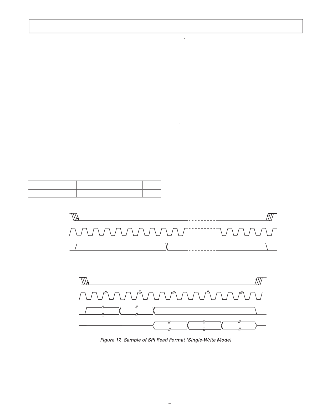
BYTE 0
BYTE 1
BYTE 4
CDATA
CCLK
CLATCH
BYTE 0
CDATA
CCLK
CLATCH
COUT
BYTE 1
HI-Z
DATA
XXX
DATA
DATA
HI-
Z
The AD1954 has many different control options. Most signal
processing parameters are controlled by writing new values to
the parameter RAM using the SPI port. Other functions, such as
volume and de-emphasis ltering, are programmed by writing to
the SPI control registers.
The SPI port uses a 4-wire interface, consisting of CLATCH,
low at the beginning of a transaction and high at the end of a
transaction. The CCLK signal latches the serial input data on a
low-to-high transition. The CDATA signal carries the serial input
data, and the COUT signal is the serial output data. The COUT
signal remains three-stated until a read operation is requested.
This allows other SPI compatible peripherals to share the same
readback line.
The SPI port is capable of full read/write operation for all of the
memories (parameter and program) and some of the SPI registers
may be accessed in both a single address mode or in burst mode.
All SPI transactions follow the same basic format that is shown in
Table I.
Table I. SPI Word Format
Byte 0
Byte 1
Byte 2
Byte 3
Byte 4
W
, Addr[9:8]
Addr[7:0]
Data
Data
Data
The R/
W
bit is low for a write and high for a read operation.
The 10-bit address word is decoded into either a location in one
of the two memories (parameter or program) or one of the SPI
registers. The number of data bytes varies according to the regis-
ter or memory being accessed. In burst-write mode (available for
loading the RAMs only), an initial address is given followed by a
continuous sequence of data for consecutive RAM locations. The
detailed data format diagram for continuous-mode operation is
given in SPI read/write data formats.
A sample timing diagram for a single SPI write operation to the
parameter RAM is shown in Figure 16.
A sample timing diagram of a single SPI read operation is shown
in Figure 17. The COUT pin goes from three-state to driven at
the beginning of Byte 2. Bytes 0 and 1 contain the address and
R/
W
bit, and Bytes 2 through 4 carry the data. The exact format
is shown in Tables VIII to XIX.
The AD1954 has several mechanisms for updating signal-processing
parameters in real time without causing loud pops or clicks. In
cases where large blocks of data need to be downloaded, the DSP
core can be shut down and new data loaded, and then the core
can be restarted. The shutdown and restart mechanisms employ a
gradual volume ramp to prevent clicks and pops. In cases where
only a few parameters need to be changed (e.g., a single biquad
lter), a safeload mechanism is used, which allows a block of SPI
registers to be transferred to the parameter RAM within a single
internal logic to prevent contention between the DSP core and
the SPI port.

AD1954
–20
Table II. SPI Port Address Decoding
Register Name
Read/Write Word Length
Parameter RAM
Write: 22 Bits
Read: 22 Bits
Write: 11 Bits
Read: 2 Bits
Write: 9 Bits
Read: N/A
Volume Left
Write: 22 Bits
Read: N/A
Volume Right
Write: 22 Bits
Read: N/A
Volume Sub
Write: 22 Bits
Read: N/A
Data Capture (SPI Out) #1
Write: 9-Bit Program Counter Value, 2-Bit Register Address
Read: 24 Bits
Data Capture (SPI Out) #2
Write: 9-Bit Program Counter Value, 2-Bit Register Address
Read: 24 Bits
Data Capture (Serial Out) Left
Write: 9-Bit Program Counter Value, 2-Bit Register Address
Read: N/A
Data Capture (Serial Out) Right
Write: 9-Bit Program Counter Value, 2-Bit Register Address
Read: N/A
Parameter RAM Safe Load Register 0
Write: 8-Bit Parameter RAM Address, 22-Bit Parameter Data
Read: N/A
Parameter RAM Safe Load Register 1
Write: 8-Bit Parameter RAM Address, 22-Bit Parameter Data
Read: N/A
Parameter RAM Safe Load Register 2
Write: 8-Bit Parameter RAM Address, 22-Bit Parameter Data
Read: N/A
Parameter RAM Safe Load Register 3
Write: 8-Bit Parameter RAM Address, 22-Bit Parameter Data
Read: N/A
Parameter RAM Safe Load Register 4
Write: 8-Bit Parameter RAM Address, 22-Bit Parameter Data
Read: N/A
Unused
Test Register
Write: 8 Bits
Read: N/A
Program RAM
Write: 35 Bits
Read: 35 Bits
Table II shows the address decoding used in the SPI port. The
one for holding signal processing parameters and one for hold-
ing the program instructions. Both of the RAMs are loaded on
power-up from on-board boot ROMs.
serial modes, de-emphasis, mute, power-down, and SPI-to-
memory transfers. Table III documents the contents of this register.
Table IV details the two bits in the register’s read operation.
Bits 1:0 set the word length, which is used in right-justi ed serial
modes to determine where the MSB is located relative to the start
of the audio frame.
Bits 3:2 select one of four serial modes, which are discussed in
the Serial Data Input Port section.
The de-emphasis curve selection Bits 5:4 turn on the internal
de-emphasis lter for one of three possible sample rates.
Bit 6, the soft power-down bit, stops the internal clocks to the DSP
core, but does not reset the part. The digital power consumption
is reduced to a low level when this bit is asserted. Reset can only
be asserted using the external reset pin.
If the initial volume was set to 1.0, this operation will take 512
sequence is initiated until the volume returns to its original setting.
When set, Bit 8 enables the DCSOUT pin. This must be set in
order to read from the data capture serial out registers.

AD1954
The initiate-safe-transfer Bit 9 will request a data transfer from
the SPI safeload registers to the parameter RAM. The safeload
registers contain address-data pairs, and only those registers
that have been written to since the last transfer operation will be
uploaded. The user may poll for this operation to complete by
reading Bit 0 of Control Register 1. The Safeload Mechanism
section goes into more detail on this feature.
Bit 10, the halt program bit, is used to initiate a volume ramp-down
followed by a shutdown of the DSP core. The user may poll for
this operation to complete by reading Bit 1 of Control Register 1.
Bit 11 sets the function of the de-emphasis/auxiliary serial input
pin. When this bit is set to 1, the pin will function as an auxiliary
serial input that is clocked by the input mux’s selected clocks.
When set to 0, this pin enables the 44.1 kHz de-emphasis curve.
Table III. Control Register 1 Write De nition
Register Bits
Function
De-emphasis/Auxiliary Serial Input Pin Select
Halt Program (1 = Halt)
Initiate Safe Transfer (1 = Transfer)
Enable DCSOUT Output Pin (1 = Enable)
De-emphasis Curve Select
3:2
Word Length
Table IV. Control Register 1 Read De nition
Register Bits
Function
DSP Core Shutdown Complete
Bit 0 is asserted when all requested safeload registers have been
transferred to the parameter RAM. It is cleared after the read
operation is complete.
Bit 1 is asserted after the requested shutdown of the DSP is com-
pleted. When this bit is set, the user is free to write or read any
RAM location without causing an audio pop or click.
Table V. Control Register 2 Write De nition
Register Bits
Function
Volume Ramp Speed
MCLK Input Select
3
Reserved
MCLK in Frequency Select
S
f
S
MCLK Out Frequency Select
S
S
Table V documents the contents of Control Register 2. Bits 1 and 0
set the frequency of the MCLKOUT pin. If these bits are set to
S
, which is the same as
the internal master clock used by the DSP core. When set to 10,
this pin is set to 256
f
S
, derived by dividing the internal DSP
clock by 2. In this mode, the output 256 f
S
clock will be inverted
with respect to the input 256 f
S
clock. This is not the case with the
feedthrough mode. When set to 11, the MCLKOUT pin mirrors
the selected MCLK input pin (it’s the output of the MCLK mux
selector). Note that the internal DSP master clock may either be
the same as the selected MCLK pin (when MCLK frequency
select is set to 512
S
mode) or may be derived from the MCLK
pin using an internal clock doubler (when MCLK frequency
select is set to 256
f
S
).
Bit 2 selects one of two possible MCLK input frequencies. When
set to 0 (default), the MCLK frequency is set to 512
S
mode, the internal DSP clock and the external MCLK are at the
same frequency. When set to 1, the MCLK frequency is set to
S
, and an internal clock doubler is used to generate the
DSP clock.
Bits 5 and 4 select one of three clock input sources using an inter-
nal mux. To avoid click and pop noises when switching MCLK
sources, it is recommended that the user put the DSP core in
shutdown before switching MCLK sources.
Bits 7 and 6 select one of three serial input sources using an
internal mux. Each source selection includes a separate SDATA,
LRCLK, and BCLK input. To avoid click and pop noises when
switching serial sources, it is recommended that the user put the
DSP core in shutdown before writing to these bits.

AD1954
Bit 8 is used to enable the three serial output pins. These pins are
connected to the output of the serial input mux, which is set by
Bits 7 and 6. The default is 0 (disabled).
Bit 9 changes the default setting of the volume ramp speed. When
set to 0, it will take 1024 LRCLK periods to go from full volume
will take 8192 LRCLK periods.
Volume Registers
The AD1954 contains three 22-bit volume registers: one each for
the left, right, and subwoofer channels. These registers are special
because when the volume is changed from an initial value to a
new value, a linear ramp is used to interpolate between the two
values. This feature prevents audible clicks and pops when chang-
ing volume. The ramp is set so that it takes 512 audio frames to
decrement from a volume of 1.0 (default) down to 0 (muted).
The volume registers are formatted in 2.20 twos complement,
meaning that 0100000000000000000000 is interpreted as 1.0.
Negative values can also be written to the volume register, caus-
ing an inversion of the signal. Negative values work as expected
with the ramp feature; to go from +1.0 to –1.0 will take 1024
LRCLKs, and the volume will pass through 0 on the way.
Parameter RAM Contents
Table VI shows the contents of the parameter RAM for the AD1954’s
default program. The parameter RAM is 22 bits wide and occupies
used to control the biquad lters. There are 22 biquad lters in all,
usage of 110 coef cients. There are also two tables of 33 coef -
cients, each that de ne the main and subcompressor input/output
characteristics. These are loaded with 1.0 on power-up, resulting
in no compression. Other RAM entries control other compressor
characteristics, as well as delay and spatialization settings.
The parameter RAM is initialized on power-up by an on-board
boot ROM. The default values yield no equalization, no com-
pression, no spatialization, no delay, and normal detector time
constants in the compressor sections. The functionality of the
AD1954 on power-up is basically that of a normal audio DAC
with no signal processing capability.
The data format of the parameter RAM is twos complement
The parameter and program RAMs can be written and read using
one of several methods.
Direct read/write. This method allows direct access to the
RAMs. Since the RAMs are also being used during real-time
DSP operation, a glitch will likely occur at the output. This
method is not recommended.
Direct read/write after core shutdown. This method avoids
the glitch while accessing the internal RAMs by rst shutting
down the core. This is recommended for transferring large
power-up or downloading a completely new program. These
transfers can be sped up by using burst mode, where an initial
3.
with address/data intended for the parameter RAM. The data
is then transferred to the requested address when the RAM is
not busy. This method can be used for dynamic updates while
live program material is playing through the AD1954. For
example, a complete update of one biquad section can occur in
one audio frame while the RAM is not busy. This method is not
The next section discusses these options in more detail.
When writing large amounts of data to the program or parameter
RAM, the processor core should be halted to prevent unpleasant
noises from appearing at the audio output. Figure 18 shows a
graphical representation of this mechanism’s volume envelope.
Points A through D are referenced in the following description.
Bit 10 in Serial Control Register 0 (processor shutdown bit) will
shut down the processor core. When the processor shutdown bit
is asserted (A), an automatic volume ramp-down sequence
down of the core. This method of shutting down the core
prevents pops or clicks from occurring. After the shutdown is
complete, Bit 1 in Control Register 1 will be set. The user can
either poll for this bit to be set or just wait for a period longer
than 20 ms.
may be written or read freely. To facilitate the transfer of large
blocks of sequential data, a block transfer mode is supported
where a starting address followed by a stream of data is sent to the
memory. The address into the memory will be automatically
incremented for each new write. This mode is documented in the
A DC
B

AD1954
–23
NOTES
The detector hold and decay times are integer values, while the rest of the parameters are fractional twos complement values.
The default decay time of the hold/release circuit is set fast enough so that the decay is dominated by the time constant of the rms detector.
Table VI. Parameter RAM Contents—Default Program
IIR0 Left b0
IIR0 Left b1
IIR0 Left b2
3
IIR0 Left a1
4
IIR0 Left a2
IIR1 Left b0
IIR1 Left b1
IIR1 Left b2
IIR1 Left a1
IIR1 Left a2
IIR2 Left b0
IIR2 Left b1
IIR2 Left b2
IIR2 Left a1
IIR2 Left a2
IIR3 Left b0
IIR3 Left b1
IIR3 Left b2
IIR3 Left a1
IIR3 Left a2
IIR4 Left b0
IIR4 Left b1
IIR4 Left b2
IIR4 Left a1
IIR4 Left a2
IIR5 Left b0
IIR5 Left b1
IIR5 Left b2
IIR5 Left a1
IIR5 Left a2
30
IIR6 Left b0
31
IIR6 Left b1
32
IIR6 Left b2
33
IIR6 Left a1
34
IIR6 Left a2
35
IIR0 Right b0
36
IIR0 Right b1
37
IIR0 Right b2
38
IIR0 Right a1
39
IIR0 Right a2
40
IIR1 Right b0
IIR1 Right b1
IIR1 Right b2
43
IIR1 Right a1
IIR1 Right a2
45
IIR2 Right b0
46
IIR2 Right b1
IIR2 Right b2
48
IIR2 Right a1
49
IIR2 Right a2
IIR3 Right b0
IIR3 Right b1
IIR3 Right b2
IIR3 Right a1
Default Value
in Fractional
Addr
Function
2.20 Format
IIR3 Right a2
IIR4 Right b0
IIR4 Right b1
IIR4 Right b2
IIR4 Right a1
IIR4 Right a2
IIR5 Right b0
IIR5 Right b1
IIR5 Right b2
IIR5 Right a1
IIR5 Right a2
IIR6 Right b0
IIR6 Right b1
IIR6 Right b2
IIR6 Right a1
IIR6 Right a2
IIR0 Xover Left b0
IIR0 Xover Left b1
IIR0 Xover Left b2
IIR0 Xover Left a1
IIR0 Xover Left a2
IIR1 Xover Left b0
IIR1 Xover Left b1
IIR1 Xover Left b2
IIR1 Xover Left a1
IIR1 Xover Left a2
IIR0 Xover Right b0
IIR0 Xover Right b1
IIR0 Xover Right b2
IIR0 Xover Right a1
IIR0 Xover Right a2
IIR1 Xover Right b0
IIR1 Xover Right b1
IIR1 Xover Right b2
IIR1 Xover Right a1
IIR1 Xover Right a2
IIR0 Xover Sub b0
IIR0 Xover Sub b1
IIR0 Xover Sub b2
IIR0 Xover Sub a1
IIR0 Xover Sub a2
IIR1 Xover Sub b0
IIR1 Xover Sub b1
IIR1 Xover Sub b2
IIR1 Xover Sub a1
IIR1 Xover Sub a2
IIR2 Xover Sub b0
IIR2 Xover Sub b1
IIR2 Xover Sub b2
IIR2 Xover Sub a1
IIR2 Xover Sub a2
IIR Sub rms b0
IIR Sub rms b1
IIR Sub rms b2
Default Value
in Fractional
Addr
Function
2.20 Format
IIR Sub rms a1
IIR Sub rms a2
Main Compressor
Look-Up Table Base
Main Compressor
10
Attack/rms Time
Main Post-
Look-Up Table Base
10
Attack/rms Time
Post-Compressor
Gain (Sub)
High-Pass Filter
Main Compressor
Look-Ahead Delay
Delay Left
Delay Right
Delay Sub
Frequency Control
Reinjection
to Main Left
Reinjection
to Main Right
Input Gain from
Left In
Input Gain from
Right In
Main Detector Hold
Time, Samples
Time, Samples
Main Detector
Decay Time
2
Decay Time
2
Unused
Default Value
in Fractional
Addr
Function
2.20 Format

AD1954
that lasts for 10 ms to 20 ms. Again, this reduces the chance of
Note that this shutdown sequence assumes that the part is set
to the fast volume ramp speed (Control Register 2, Bit 9). If the
slow ramp speed is set, the volume may not reach zero before the
part enters shutdown and a click or pop may be heard.
Many applications require real-time control of lter characteristics,
such as bass/treble controls and parametric or graphic equalization.
To prevent instability from occurring, all of the parameters of a
particular biquad lter must be updated at the same time; other-
wise, the lter could execute for one or two audio frames with a
mixture of old and new coef cients. This mix of old and new
could cause temporary instability, leading to transients that could
take a long time to decay.
The method used in the AD1954 to eliminate this problem is to
load a set of ve registers in the SPI port with the desired param-
eter RAM address and data. Five registers are used because each
biquad lter has ve coef cients. Once these registers are loaded,
the initiate safe transfer bit in Control Register 1 should be set.
the program sequence where the parameter RAM is not being
program counter reaches this point, the parameter RAM is writ-
ten with ve new data values at addresses corresponding to those
that were entered in the safeload registers. When the operation is
complete, Bit 0 of Control Register 1 (read) is set. This bit may
be polled by the external microprocessor until a 1 is read and
will be reset on a read operation. The polling operation is not
required; the safeload mechanism guarantees that the transfer will
be complete within one audio frame.
The safeload logic automatically sends only those safeload registers
that have been written to since the last safeload operation. For
example, if only two parameters are to be sent, then it is neces-
sary to write to only two of the ve safeload registers. When the
request safe transfer bit is asserted, only those two registers will
be sent; the other three registers are not sent and can still hold
old or invalid data.
The safeload mechanism is not limited to uploading biquad
coef cients; any set of ve values in the parameter RAM may be
updated in the same way. This allows real-time adjustment of the
compressor/limiter, delay, or stereo spreading blocks.
Table VII shows the sizes and available modes of the parameter
RAM and the program RAM.
The read/write formats of the SPI port are designed to be byte-
oriented. This allows for easy programming of common microcon-
troller chips. To t into a byte-oriented format, 0s are appended
to the data elds to extend the data-word to the next multiple of
RAM are appended with two leading zeroes to reach 24 bits
extended data elds are appended to a 2-byte eld consisting of a
read/write bit and a 10-bit address. The SPI port knows how many
data bytes to expect based on the address that is received in the
rst two bytes.
The total number of bytes for a single-location SPI write command
can vary from 4 bytes (for a control register write) to 7 bytes (for
locations in program RAM or parameter RAM.
The read and write formats of the parameter RAM, program RAM
Table VII. Read/Write Modes
Burst Mode
Memory
Range
Read
Write
Available
Write Modes
Parameter RAM
Yes
Yes
Yes
Direct write, write after core shutdown, safeload write
Program RAM
35
Yes
Yes
Yes
Direct write, write after core shutdown
Table VIII. Parameter RAM Read/Write Format (Single Address)
Byte 0
Byte 1
Byte 2
Byte 3
Byte 4
W
, Addr[9:8]
Addr[7:0]
Param[15:8]
Param[7:0]
Table IX. Parameter RAM Block Read/Write Format (Burst Moded)
Byte 0
Byte 1
Byte 2
Byte 3
Byte 4
W
, Addr[9:8]
Addr[7:0]
Param[15:8]
Param[7:0]
Table X. Program RAM Read/Write Format (Single Address)
Byte 0
Byte 1
Byte 2
Byte 3
Byte 4
Byte 5
Byte 6
W
, Addr[9:8]
Addr[7:0]
Prog[31:24]
Prog[23:16]
Prog[15:8]
Prog[7:0]
Byte 5
Byte 8
Byte 6
Byte 9
Byte 7
Byte 10
ADDR + 1 ADDR + 2

AD1954
–25
Byte 7
Byte 12
Byte 8
Byte 13
Byte 9
Byte 14
Byte 10
Byte 15
Byte 11
Byte 16
ADDR + 1 ADDR + 2
Table XI. Program RAM Read/Write Format (Burst Address)
Byte 0
Byte 1
Byte 2
Byte 3
Byte 4
Byte 5
Byte 6
W
, Addr[9:8]
Addr[7:0]
Prog[31:24]
Prog[23:16]
Prog[15:8]
Prog[7:0]
Table XII. SPI Control Register 1 Write Format
Byte 0
Byte 1
Byte 2
Byte 3
W
, Addr[9:8]
Addr[7:0]
Bit[7:0]
Table XIII. SPI Control Register 1 Read Format
Byte 0
Byte 1
Byte 2
W
, Addr[9:8]
Addr[7:0]
Table XIV. SPI Control Register 2 Write Format
Byte 0
Byte 1
Byte 2
Byte 3
W
, Addr[9:8]
Addr[7:0]
Bit[7:0]
Table XV. SPI
Volume Register Write Format
Byte 0
Byte 1
Byte 2
Byte 3
Byte 4
Addr[7:0]
Volume[15:8]
Volume[7:0]
Table XVI. Data Capture Register Write Format
Byte 0
Byte 1
Byte 2
Byte 3
W
, Addr[9:8]
Addr[7:0]
ProgCount[5:0], RegSel[1:0]
NOTES
ProgCount[8:0] = value of program counter where trap occurs (see Table XX).
RegSel[1:0] selects one of four registers (see Data Capture Register section).
Table XVII. Data Capture Serial Out Register (Address and Register Select) Write Format
Byte 0
Byte 1
Byte 2
Byte 3
W
, Addr[9:8]
Addr[7:0]
ProgCount[5:0], RegSel[1:0]
NOTES
ProgCount[8:0] = value of program counter where trap occurs (see Table XX).
RegSel[1:0] selects one of four registers (see Data Capture Register section).
Table XVIII. Data Capture Read Format
Byte 0
Byte 1
Byte 2
Byte 3
Byte 4
Byte 5
W
, Addr[9:8]
Addr[7:0]
Data[23:16]
Data[15:8]
Data[7:0]
Table XIX. Safeload Register Write Format
Byte 0
Byte 1
Byte 2
Byte 3
Byte 4
Byte 5
W
, Addr[9:8]
Addr[7:0]
ParamAddr[7:0]
Param[15:8]
Param[7:0]

AD1954
–26
INITIALIZATION
Power-Up Sequence
The AD1954 has a built-in power-up sequence that initializes the
contents of the internal RAMs. During this time, the contents
of the internal program boot ROM are copied to the internal
program RAM memory, and likewise, the SPI parameter RAM is
lled with values from its associated boot ROM. The data memo-
ries are also cleared during this time.
The boot sequence lasts for 1024 MCLK cycles and starts on the
rising edge of the RESETB pin. Since the boot sequence requires
from the SPI registers during this period of time. Note that the
default power-on state of the internal clock mode circuitry is 512
S
, or about 24 MHz for normal audio sample rates. This mode
bypasses all the internal clock doublers and allows the external
master clock to directly operate the DSP core. If the external
master clock is 256
f
S
, then the boot sequence will operate at
this reduced clock rate and will take slightly longer to complete.
After the boot sequence has nished, the clock modes may be
set via the SPI port. For example, if the external master clock
frequency is 256
f
S
clock, the boot sequence would take 1024
S
clock cycles to complete, after which an SPI write could
occur to put the AD1954 in 256
S
mode.
The default state of the MCLK input selector is MCLK0. Since
this input selector is controlled using the SPI port, and the SPI port
cannot be written to until the boot sequence is complete, there
must be a stable master clock signal present on the MCLK0 pin at
startup.
The AD1954 contains a clock doubler circuit that is used to gener-
f
S
clock when the external clock is 256
f
S
The clock mode is set by writing to Bit 2 of Control Register 2.
When the clock mode is changed, it is possible that a glitch will
occur on the internal MCLK signal. This may cause the proces-
sor to inadvertently write an incorrect value into the data RAM,
which could cause an audio pop or click sound. To prevent this
the following procedure is recommended:
Assert the soft power-down bit (Bit 6 in Control Register 1) to
stop the internal MCLK.
Write the desired clock mode into Bit 2 of Control Register 2.
3.
Wait at least 1 ms while the clock doublers settle.
4.
De-assert the soft power-down bit.
An alternative procedure is to initiate a soft shutdown of the pro-
cessor core by writing a 1 to the halt program bit in Control
Register 1. This initiates a volume ramp-down sequence followed
by a shutdown of the DSP core. Once the core is shut down (which
can be veri ed by reading Bit 1 from Control Register 1 or by
waiting at least 20 ms), the new clock mode can be programmed
by writing to Bit 2 of Control Register 2. The DSP core can then
be restarted by clearing the halt program bit in Control Register 1.
The AD1954 contains input selectors for both serial data inputs
of input and clock sources with no external hardware required.
These input selectors are controlled by writing to SPI Control
Register 2.
When the data source or MCLK source is changed by writing
to the SPI port, it is possible that a pop or click will occur in the
writing a 1 to the halt program bit in Control Register 1. This
initiates a volume ramp-down sequence followed by a shutdown
of the DSP core. Once the core is shut down (which can be veri-
ed by reading Bit 1 from Control Register 1 or by waiting at
least 20 ms after the halt program command is issued), the new
data or MCLK source can be programmed by writing to Control
Register 2. The DSP core can then be restarted by clearing the
halt program bit in Control Register 1.
DATA CAPTURE REGISTERS
The AD1954 incorporates a feature called data capture. Using
this feature, any node in the signal processing ow may be sent
to either an SPI readable register or a dedicated serial output
pin. This allows the basic functionality of the AD1954 to be
extended to a larger number of channels. Alternatively, it can be
used to monitor and display information about signal levels or
compressor/limiter activity.
The AD1954 contains four independent data capture registers.
Two of these registers transfer their data to the data capture serial
output (DCSOUT) pin. The serial data format of this pin is the
same as the serial data format used for the main digital inputs,
frame sync and bit clock signals. This pin is primarily intended
to feed signals to an external DAC or DSP chip to extend the
number of channels that the internal DSP can access. The other
two registers may be read back over the SPI port and can be used
for a variety of purposes. One example might be to access the dB
output of the internal rms detector to run a front-panel signal
level display. A sample system is shown in Figure 19. For each
of the four data capture registers, a capture count and a register
select must be set. The capture count is a number between 0 and
capture will occur. The register select eld programs one of four
registers in the DSP core that will be transferred to the data cap-
ture register when the program counter equals the capture count.
The register select eld is decoded as follows:
The capture count and register select bits are set by writing to one
of the four data capture registers at the following SPI addresses:
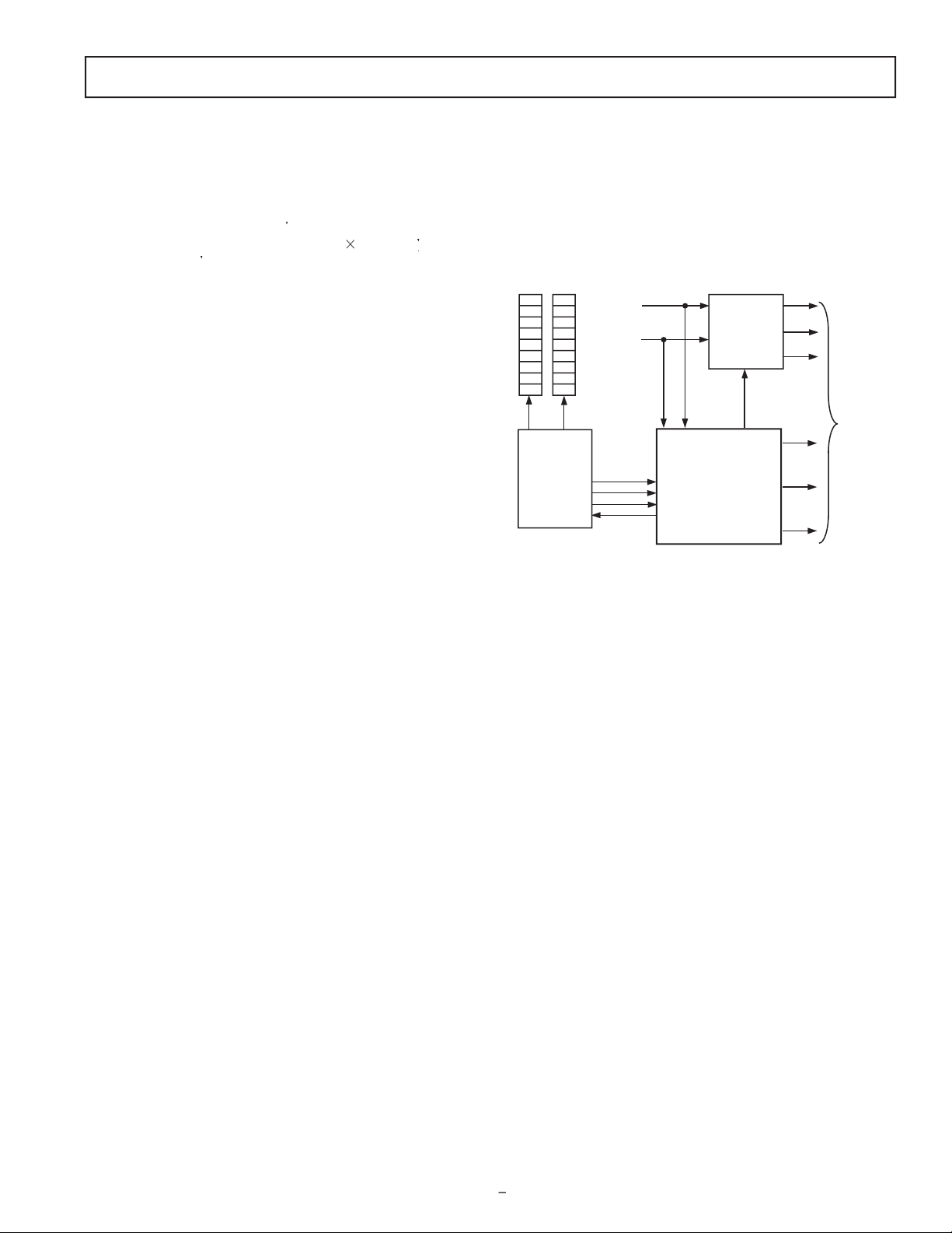
AD1954
The format of the captured data varies according to the register
select elds. Data captured from the mult_out setting is in 1.23
twos complement format so that a full-scale input signal will
produce a full-scale digital output (assuming no processing). If
the parameters are set such that the input-to-output gain is more
than 0 dB, then the digital output will be clipped.
Data captured from the
DB_OUT
setting is in 5.19 format, where
the actual rms dB level is equal to –87 + (3
DB_OUT
). In this
equation,
DB_OUT
is the value that is captured. It follows that in
this data format, the actual output readings will range from –87 dB
to +9 dB. The AD1954 uses the convention that 0 dB is the rms
value of the full-scale digital signal.
Data captured using the MDI setting is in 3.21 format. A 0 dB
digital input will produce a –12 dB digital output, assuming the
AD1954 is set for no processing.
Data captured using the MCI setting is in 2.20 format. This data
is generally a signal gain or lter coef cient, and therefore it does
not make sense to talk about the input-to-output gain. A coef -
cient of 01000000000000000000 corresponds to a gain of 1.0.
The data that must be written to set up the data capture is a
concatenation of the 9-bit program count index with the 2-bit
register select eld. Refer to Table XX to nd the capture count
to be monitored in the default signal processing ow.
The SPI capture registers can be accessed by reading from SPI
Locations 261 (for SPI Capture Register 1) or 262 (for SPI Cap-
ture Register 2). The other two data capture registers (data capture
serial out) automatically transfer their data to the data capture
serial out (DCSOUT) pin. DCSOUT Capture Register 1 is pres-
ent in the left data slot (as de ned by the serial input format), and
DCSOUT Capture Register 2 is present in the right data slot. The
format for writing to the SPI data capture setup registers is given
in the SPI section of this data sheet.
DCSOUT
LRCLK
BCLK
dB LEVEL METERS
MICRO-
CONTROLLER
AD1954
EXT DACs
5.1
CHANNEL
OUTPUT

AD1954
–28
Table XX. Data Capture Trap Indexes and Register Select—Default Program
Program Count
Register
Index (9 Bits)
Numeric Format
HPF Out Left
Mult_Out
HPF Out Right
Mult_Out
De-emphasis Out Left
Mult_Out
De-emphasis Out Right
Mult_Out
Left Biquad 0 Output
34
Mult_Out
Left Biquad 1 Output
43
Mult_Out
Left Biquad 2 Output
Mult_Out
Left Biquad 3 Output
Mult_Out
Left Biquad 4 Output
Mult_Out
Left Biquad 5 Output
Mult_Out
Left Biquad 6 Output
Mult_Out
Right Biquad 0 Output
Mult_Out
Right Biquad 1 Output
Mult_Out
Right Biquad 2 Output
302
Mult_Out
Right Biquad 3 Output
311
Mult_Out
Right Biquad 4 Output
320
Mult_Out
Right Biquad 5 Output
329
Mult_Out
Right Biquad 6 Output
338
Mult_Out
Volume Out Left
Mult_Out
Volume Out Right
Mult_Out
Volume Out Sub
459
Mult_Out
Phat Stereo Out Left
Mult_Out
Phat Stereo Out Right
Mult_Out
Delay Output Left
Mult_Out
Delay Output Right
361
Mult_Out
Main Compressor rms Out (dB)
DB_Out
Main Compressor Gain Reduction
MCI
(Linear)
Look-Ahead Delay Output Left
MDI
3.21, 2 LSBs Truncated
Look-Ahead Delay Output Right
3.21, 2 LSBs Truncated
Main Compressor Out Left
Mult_Out
Main Compressor Out Right
Mult_Out
Interpolator Input Left
Mult_Out
(Includes Sub Reinject)
Interpolator Input Right
362
Mult_Out
(Includes Sub Reinject)
430
Mult_Out
438
Mult_Out
Mult_Out
456
Mult_Out
Left Xover Biquad 0 Output
Mult_Out
Left Xover Biquad 1 Output
Mult_Out
Right Xover Biquad 0 Output
Mult_Out
Right Xover Biquad 1 Output
Mult_Out
Mult_Out
467
Mult_Out
489
DB_Out
24-Bit Positive Binary, Bit 19
Corresponds to a 3 dB Change
495
MCI
2.22, 2 LSBs = 0
Mult_Out
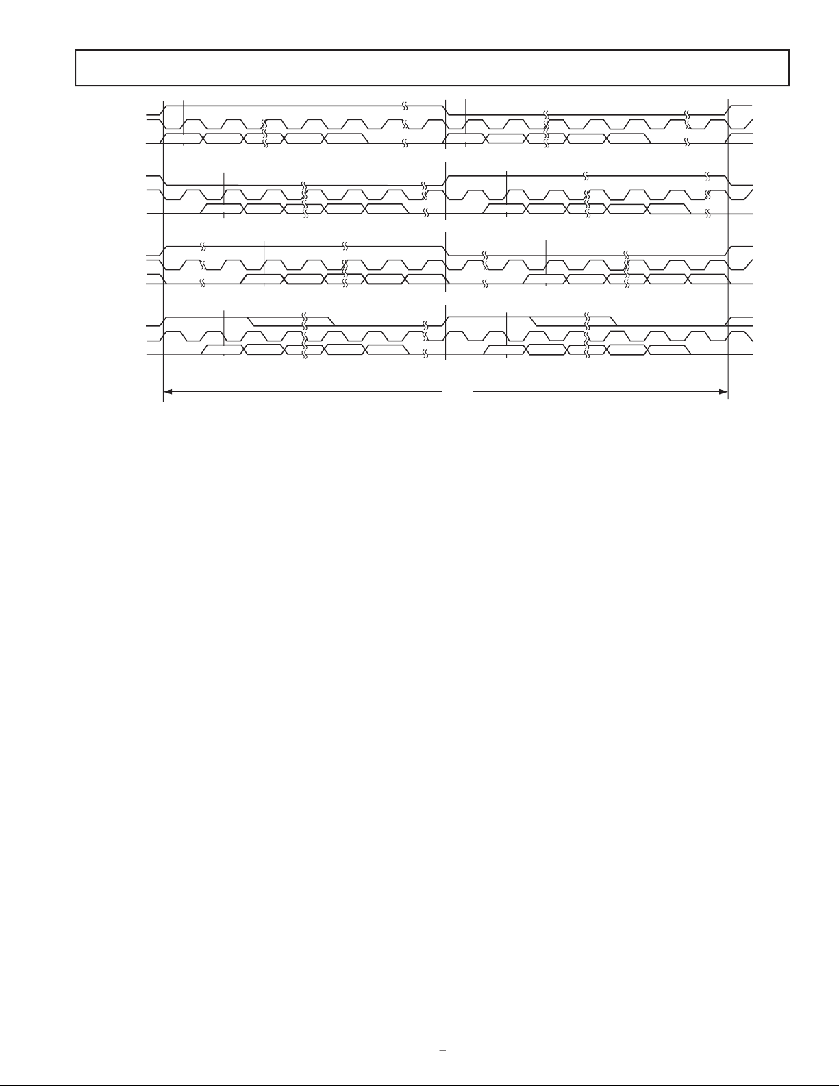
AD1954
–29
The AD1954’s exible serial data input port accepts data in twos
complement, MSB rst format. The left channel data eld always
precedes the right channel data eld. The serial mode is set by
using mode select bits in the SPI control register. In all modes
except for the right-justi ed mode, the serial port will accept an
cause an error, but they will be truncated internally). In the right-
justi ed mode, SPI control register bits are used to set the word
length to 16 bits, 20 bits, or 24 bits. The default on power-up is
exactly 64 BCLKs per audio frame.
Figure 20 shows the serial input modes. For the left-justi ed
mode, LRCLK is high for the left channel and low for the right
channel. Data is sampled on the rising edge of BCLK. The MSB
is left-justi ed to an LRCLK transition, with no MSB delay. The
left-justi ed mode can accept any word length up to 24 bits.
2
the right channel. Data is valid on the rising edge of BCLK. The
MSB is left-justi ed to an LRCLK transition but with a single
BCLK period delay. The I
number of bits up to 24.
In right-justi ed mode, LRCLK is high for the left channel and low
for the right channel. Data is sampled on the rising edge of BCLK.
The start of data is delayed from the LRCLK edge by 16 BCLK,
length. The default word length is 24 bits; other word lengths are set
by writing to Bits 1 and 0 of Control Register 1. In right-justi ed
mode, it is assumed that there are 64 BCLKs per frame.
For the DSP serial port mode, LRCLK must pulse high for at
least one bit clock period before the MSB of the left channel
is valid, and LRCLK must pulse high again for at least one bit
clock period before the MSB of the right channel is valid. Data is
sampled on the falling edge of BCLK. The DSP serial port mode
can be used with any word length up to 24 bits. In this mode,
it is the responsibility of the DSP to ensure that the left data is
transmitted with the rst LRCLK pulse and that synchronism is
maintained from that point forward.
DIGITAL CONTROL PINS
Mute
The AD1954 offers two methods of muting the analog output.
By asserting the mute signal high, the left, right, and subchan -
nels are muted. As an alternative, the user can assert the mute
bit in the serial control register high. The AD1954 has been
designed to minimize pops and clicks when muting and unmut-
ing the device by automatically ramping the gain up or down.
When the device is unmuted, the volume returns to the value
set in the volume register.
De-emphasis
The AD1954 has a built-in de-emphasis lter that can be used to
decode CDs that have been encoded with the standard redbook
vated by the pin or by an SPI write to the control register. When
RIGHT CHANNEL
LEFT CHANNEL
LRCLK
BCLK
SDATA
LSB LSB
LSB
LSB
LSB
LSB
LSB
LSB
LEFT CHANNEL
RIGHT CHANNE
L
LRCLK
BCLK
SDATA
LRCLK
BCLK
SDATA
LRCLK
BCLK
SDATA
1/f
S
DSP MODE – 16 BITS TO 24 BITS PER CHANNEL
NOTES
1. DSP MODE DOESN’T IDENTIFY CHANNEL.
2. LRCLK NORMALLY OPERATES AT fS EXCEPT DSP MODE, WHICH IS 2 fS.
3. BCLK FREQUENCY IS NORMALLY 64 LRCLK BUT MAY BE OPERATED IN BURST MODE.
MSB
MSB
MSB
MSB
MSB MSB
MSB
MSB
LEFT-JUSTIFIED MODE – 16 BITS TO 24 BITS PER CHANNEL
I2S MODE – 16 BITS TO 24 BITS PER CHANNEL
RIGHT-JUSTIFIED MODE – SELECT NUMBER OF BITS PER CHANNE
L

AD1954
–30
ANALOG OUTPUTSECTION
Figure 21 shows the block diagram of the analog output section.
A series of current sources are controlled by a digital
modu-
lator. Depending on the digital code from the modulator, each
current source is connected to the summing junction of either a
positive I-to-V converter or a negative I-to-V converter. Two extra
current sources that push instead of pull are added to set the
midscale common-mode voltage.
SWITCHED CURRENT
SOURCES
OUT+
OUT–
I
REF
I
REF
– DIG_INI
REF
+ DIG_IN
VREF IN
FROM DIGITAL
- MODULATOR
(DIG_IN)
BIAS
I
REF
All current sources are derived from the VREF input pin. The
gain of the AD1954 is directly proportional to the magnitude of
the current sources, and therefore the gain of the AD1954 is pro-
portional to the voltage on the VREF pin. With VREF set to 2.5 V,
the gain of the AD1954 is set to provide signal swings of 2 V rms
differential (1 V rms from each pin). This is the recommended
operating condition.
When the AD1954 is used to drive an audio power ampli er and
the compression feature is being used, the VREF voltage should
then be derived by dividing down the supply of the ampli er.
This sets a xed relationship between the digital signal level
sor) and the full-scale output of the ampli er (just prior to the
onset of clipping). For example, if the ampli er power supply
drops by 10%, then the VREF input to the ampli er will also
drop by 10%, which will reduce the analog output signal swing
by 10%. The compressor will therefore be effective in preventing
clipping, regardless of any variation in ampli er supply voltage.
be taken to ensure that no ac signals appear on this pin. This
can be accomplished by using a large decoupling capacitor in
the VREF external resistive divider circuit. If the VREF signal is
derived by dividing the 5 V analog supply, then the time constant
of the divider must effectively lter any noise on the supply. If
the VREF signal is derived from an unregulated power ampli er
supply, then the time constant must be longer, since the ripple on
the ampli er supply voltage will presumably be greater than in
the case of the 5 V supply.
The AD1954 should be used with an external third order lter
on each output channel. The circuit shown in Figures 22, 23, and
converter in the same circuit. The values used in the main channel
subwoofer channel (Figure 23) result in a 10 kHz Bessel lter.
1.50k
3.01k
2.80k
2.7nF
499
1.00k
806
1nF
820pF
270pF
2.2nF
549
– INPUT
+ INPUT
OUT
3.01k
11k
56nF
1.5k
5.62k
5.62k
27nF
15nF
6.8nF
220nF
604
– INPUT
+ INPUT
OUT
560nF
270nF
68pF
150pF
2.2nF
11k
The lower frequency lter is used on the subwoofer output because
there is no digital interpolation lter used in the subwoofer signal
path. When calculating the resistor values for the lter, it is impor-
tant to take into account the output resistance of the AD1954,
which is nominally 60
tors should be used. The reason for this is that the single-ended
performance of the AD1954 is about 80 dB. The degree to which
the single-ended distortion cancels in the nal output is determined
by the common-mode rejection of the external analog lter, which in
turn depends on the tolerance of the components used in the lter.
The sub output of the AD1954 has a lower drive strength than
the left and right output pins (±0.25 mA peak versus ±0.5 mA
peak for the left and right outputs). For this reason, it is best to
use higher resistor values in the external sub lter.
Figure 24 shows a recommended lter design for the subwoofer
pins used as a full bandwidth channel in a custom designed pro-
gram. This design is also a 100 kHz Bessel lter.
3.01k
11k
56nF
1.5k
5.62k
27nF
150pF
68pF
2.2nF
604
– INPUT
+ INPUT
OUT
11k
5.62k
For best performance, a large (>10 µF) capacitor should be con-
nected between the FILTCAP pin and analog ground. This pin is
connected to an internal node in the bias generator, and by add-
ing an external capacitance to this pin, the thermal noise of the
left/right channels is minimized. The sub channel is not affected
by this connection.

AD1954
–31
These graphical tools allow the user to modify the default signal
processing ow by individually placing each block (e.g., biquad
lter, Phat Stereo, dynamics processor) and connecting them in
into the AD1954’s program RAM. All of the contents of the parame-
ter RAM can also be set using these tools. For more information
on these programming tools, contact SigmaDSP@analog.com.

AD1954
–32
APPENDIX
For designing a parametric EQ, follow the steps below.
Frequency
dB_Gain
A = 10
= 2
Frequency/Sample_Rate
sn = sin(
)
)
= sn/(2
3.
b0 = ( 1 + A
)/( 1 + (
/A))
b1 = –2
cs/( 1 + (
/A))
b2 = (1 – (
A))/(1 + (
/A))
cs/(1 + (
/A)) = –b1
/A))/( 1 + (
/A))
4.
The transfer function implemented by the AD1954 is given by:
H(Z) =
Z – 1 + b2
Z – 2)/
Z – 1 – a2
Z – 2)
Note the inversion in sign of a1 and a2 relative to the more
stan dard form. This form is used in this document because
the AD1954 implements the difference equation using the
formula below.
Y(n) = a1
y(n – 1) + a2
y(n – 2) + b0
x(n)
+ b1
x(n – 1) + b2
x(n – 2)
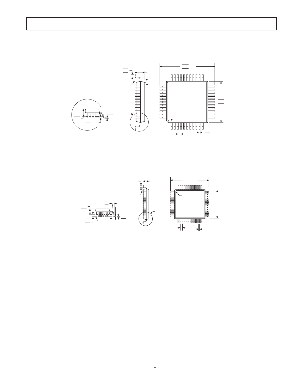
AD1954
–33
44-Lead Metric Quad Flat Package [MQFP]
Dimensions shown in millimeters
0.80
BS
C
0.45
0.29
2.45
MA
X
1.03
0.88
0.73
8
0.8
SEATING
PLANE
TOP VIEW
(PINS DOWN)
1
33
34
11
12
23
22
44
COPLANARITY
0.10
PIN 1
0.25 MAX
0.10 MI
N
VIEW A
ROTATED 90 CCW
7
0
2.20
2.00
1.80
VIEW A
13.45
13.20 SQ
12.95
10.20
10.00 SQ
9.80
COMPLIANT TO JEDEC STANDARDS MO-112-AB
48-Lead Low Pro le Quad Flat Package [LQFP]
Dimensions shown in millimeters
TOP VIEW
(PINS DOWN)
1
12
13
25
24
36
37
48
0.27
0.22
0.17
0.50
BSC
7.00
BSC SQ
SEATING
PLANE
1.60
MAX
0.75
0.60
0.45
VIEW A
9.00 BSC
SQ
PIN 1
0.20
0.09
1.45
1.40
1.35
0.08 MAX
COPLANARITY
VIEW A
ROTATED 90 CCW
SEATING
PLANE
10
6
2
7
3.5
0
0.15
0.05
COMPLIANT TO JEDEC STANDARDS MS-026BBC

AD1954
–34
Location
Page
8/03—Data Sheet changed from REV. 0 to REV. A.
. . . . . . . . . . . . . . . . . . . . . . . . . . . . . . .
. . . . . . . . . . . . . . . . . . . . . . . . . . . . . . .
. . . . . . . . . . . . . . .
3
. . . . . . . . . . . . . . . . . . . . . . . . . . . . . . .
. . . . . . . . . . . . . . . . . . . . . . . . . . . . . . .
.
. . . . . . . . . . . . . . . . . . . . . . . . . . . . . . .
. . . . . . . . . . . . . . . . . . . . . . . . . . . . . . .
. . . . . . . . . . . . .
. . . . . . . . . . . . . . . . . . . . . . . . . . . . . . .
. . . . . . . . . . . . . . . . . . . . . . . . . . . . . . .
. . . . . . . . . . . . . . . . . . . . .
. . . . . . . . . . . . . . . . . . . . . . . . . . . . . . .
. . . . . . . . . . . . . . . . . . . . . . . . . . . . . . .
. . . .
. . . . . . . . . . . . . . . . . . . . . . . . . . . . . . .
. . . . . . . . . . . . . . . . . . . . . . . . . . . . . . .
. . . . . . . . .
Replaced Control Register 1 section
. . . . . . . . . . . . . . . . . . . . . . . . . . . . . . .
. . . . . . . . . . . . . . . . . . . . . . . . . . . . . . .
. . . . . . . . . . .
. . . . . . . . . . . . . . . . . . . . . . . . . . . . . . .
. . . . . . . . . . . . . . . . . . . . . . . . . . . . . . .
. . . . . . . . .
. . . . . . . . . . . . . . . . . . . . . . . . . . . . . . .
. . . . . . . . . . . . . . . . . . . . . . . . . . . . . . .
. . .
. . . . . . . . . . . . . . . . . . . . . . . . . . . . . . .
. . . . . . . . . . . . . . . . . . . . . . . . . . . . . . .
. . . . . . . . . . . . . . . . . . . . . . . .
. . . . . . . . . . . . . . . . . . . . . . . . . . . . . . .
. . . . . . . . . . . . . . . . . . . . . . . . . . . . . . .
. . . . . . . . . . . . . . . . . . . . . . . .
. . . . . . . . . . . . . . . . . . . . . . . . . . . . . . .
. . . . . . . . . . . . . . . . . . . . . . . . . . . . . . .
. . . . . . . . . . . . . . . . . . . . . . . .
. . . . . . . . . . . . . . . . . . . . . . . . . . . . . . .
. . . . . . . . . . . . . . . . . . . . . . . . . . . . . .
. . . . . . . . . . . . . . . . . . . . . . . . . . . . . . .
. . . . . . . . . . . . . . . . . . . . . . . . . . . . . . .
. . . . . . . . . . . . . . . . . . . . . . .
. . . . . . . . . . . . . . . . . . . . . . . . . . . . . . .
. . . . . . . . . . . . . . . . . . . . . . . . . . . . . .
30
Reversed Figures 22 and 23
. . . . . . . . . . . . . . . . . . . . . . . . . . . . . . .
. . . . . . . . . . . . . . . . . . . . . . . . . . . . . . .
. . . . . . . . . . . . . . . . .
30
Added Figure 24
. . . . . . . . . . . . . . . . . . . . . . . . . . . . . . .
. . . . . . . . . . . . . . . . . . . . . . . . . . . . . . .
. . . . . . . . . . . . . . . . . . . . . . . . .
30
Updated OUTLINE DIMENSIONS
. . . . . . . . . . . . . . . . . . . . . . . . . . . . . . .
. . . . . . . . . . . . . . . . . . . . . . . . . . . . . . .
. . . . . . . . . .
33

–35

–36
 Loading...