

4 ADC/8 DAC with PLL,
www.BDTIC.com/ADI
Preliminary Technical Data
Features
PLL generated (32-192kHz) or direct master clock
Low EMI design
109 dB DAC/ 107dB ADC Dynamic Range and SNR
-94dB THD+N
Single 3.3V Supply
Tolerance for 5V logic inputs
Supports 24-bits and 8 kHz - 192 kHz sample rates
Differential ADC input
Single-ended or Differential DAC output versions
Log volume control with "auto-ramp" function
Hardware and software controllable clickless mute
Software and hardware power-down
Right justified, left justified, I
Master and slave modes up to 16 channel in/out
48-lead LQFP or 64-lead LQFP plastic package
2
S and TDM Modes
192 kHz, 24 Bit CODEC
AD1935/AD1936/AD1937/AD1938/AD1939
Applications
Automotive audio systems
Home theater systems
Set-top boxes
Digital audio effects processors
GENERAL DESCRIPTION
The
AD193X family are
provide 4 ADCs with differential input and 8 DACs with either
single-ended or differential output using ADI’s patented multibit
sigma-delta architecture. An SPI® or I2C® port is included, allowing
a microcontroller to adjust volume and many other parameters.
The
AD193X family
The
AD193X
is available in a 48-lead (SE output) or 64-lead
(differential output) LQFP package.
The AD193X is designed for low EMI. This consideration is
apparent in both the system and circuit design architectures. By
using the on-board PLL to derive master clock from L-R clock, the
AD193X eliminates the need for a separate high frequency master
clock. It can also be used with a suppressed bit clock. The D-A and
A-D converters are designed using the latest ADI continuous time
architectures to further minimize EMI. By using 3.3V supplies,
power consumption is minimized, further reducing emissions.
high performance, single-chip codecs that
operates from 3.3V digital and analog supplies.
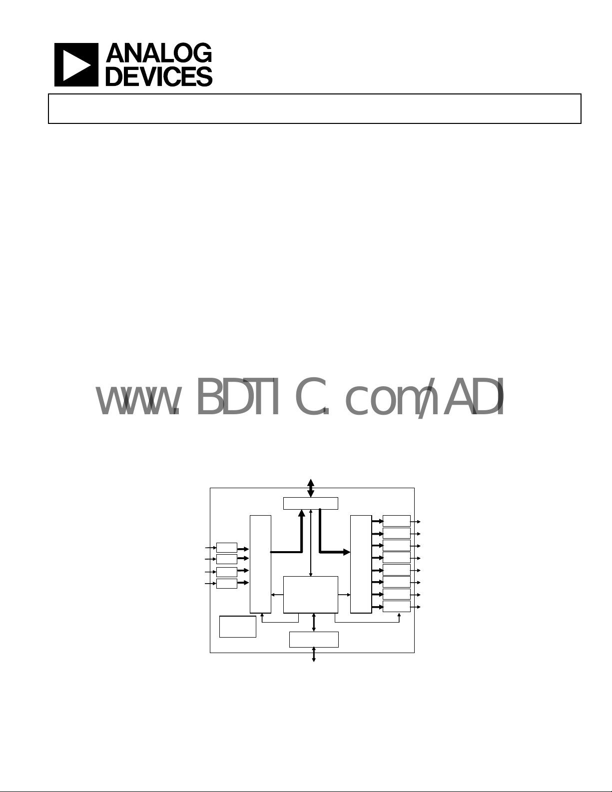
Functional Block Diagram
AD193X
AD193X
ADC
ADC
ADC
Analog
Analog
Audio
Audio
Inputs
Inputs
Rev. PrI
Information furnished by Analog Devices is believed to be accurate and reliable.
However, no responsibility is assumed by Analog Devices for its use, nor for any
infringements of patents or other rights of third parties that may result from its use.
Specifications subject to change without notice. No license is granted by implication
or otherwise under any patent or patent rights of Analog Devices. Trademarks and
registered trademarks are the property of their respective companies.
ADC
ADC
ADC
ADC
ADC
Precision
Precision
Voltage
Voltage
Reference
Reference
Digital
Digital
Filter
Filter
Timing Management
Timing Management
Digital Audio
Digital Audio
Input/Output
Input/Output
Serial Data Port
Serial Data Port
CLOCKS
CLOCKS
&
&
Control
Control
(Clock & PLL)
(Clock & PLL)
Control Port
Control Port
Control Port
2
2
2
SPI / I
SPI / I
SPI / I
C
C
C
Control Data
Control Data
Input/Output
Input/Output
Figure 1
DAC
DAC
DAC
DAC
DAC
SDATAI NSDATAOUT
SDATAI NSDATAOUT
Digital
Digital
Filter
Filter
&
&
Volume
Volume
Control
Control
DAC
DAC
DAC
DAC
DAC
DAC
DAC
DAC
DAC
DAC
DAC
Analog
Analog
Audio
Audio
Outputs
Outputs
One Technology Way, P.O. Box 9106, Norwood, MA 02062-9106, U.S.A.
Tel: 781.329.4700
www.analog.com
Fax: 781.326.8703 © 2005 Analog Devices, Inc. All rights reserved.
AD1935/AD1936/AD1937/AD1938/AD1939
www.BDTIC.com/ADI
Preliminary Technical Data
AD193X—SPECIFICATIONS
Test Conditions, Unless Otherwise Noted.
Performance of all channels is identical (exclusive of the Inter-channel Gain Mismatch and Inter-channel Phase Deviation specifications).
Parameter Rating
Supply Voltages (AVDD, DVDD) 3.3 V
Case Temperature 25°C
Master Clock 12.288 MHz (48 kHz fS, 256 × fS Mode)
Input Signal 1.000 kHz, 0 dBFS (Full Scale), -1 dBVrms (0.9Vrms)
Input Sample Rate 48 kHz
Measurement Bandwidth 20 Hz to 20 kHz
Word Width 24 Bits
Load Capacitance (Digital Output) 50 pF
Load Current (Digital Output)
Input Voltage HI 2.0 V
Input Voltage LO 0.8 V
Analog Performance
Parameter Min Typ Max Unit
ADC Resolution (all ADCs) 24 Bits
Dynamic Range (20 Hz to 20 kHz, –60 dB Input)1
No Filter (RMS) 102 dB
With A-Weighted Filter (RMS) 105 dB
With A-Weighted Filter (Avg) 107 dB
Total Harmonic Distortion + Noise (–1 dBFS)1 –92 dB
Full-Scale Input Voltage (Differential) 1.9 V rms
Gain Error –5.0 +5.0 %
ANALOG-TO-DIGITAL CONVERTERS
DIGITAL-TO-ANALOG CONVERTERS
1
Total harmonic distortion + noise and dynamic range typical specifications are for two channels active, max/min are all channels active.
Interchannel Gain Mismatch –0.1 +0.1 dB
Offset Error –10 0 +10 mV
Gain Drift 100 ppm/°C
Interchannel Isolation –110 dB
CMRR, 100 mV RMS, 1 kHz 70 dB
CMRR, 100 mV RMS, 20 kHz 70 dB
Input Resistance 14
Input Capacitance 10 pF
Input Common-Mode Bias Voltage 1.5 V
Dynamic Range (20 Hz to 20 kHz, –60 dB Input)1
No Filter (RMS), Single-ended version 101 dB
With A-Weighted Filter (RMS), Single-ended version 104 dB
With A-Weighted Filter (Avg), Single-ended version 106 dB
No Filter (RMS), Differential version 104 dB
With A-Weighted Filter (RMS), Differential version 107 dB
With A-Weighted Filter (Avg), Differential version 109 dB
Total Harmonic Distortion + Noise (0 dBFS)1
Single-ended version –92 dB
Differential version –94 dB
Full-Scale Output Voltage (Single-ended version) 0.9 (2.5) V rms (V pp)
Full-Scale Output Voltage (Differential version) 1.8 (5.0) V rms (V pp)
Gain Error -6% TBD +6% %
±1 mA or 1.5kΩ to ½ DVDD supply
Tab le 1
kΩ
Rev. PrI | Page 2 of 30
Preliminary Technical Data
www.BDTIC.com/ADI
Parameter Min Typ Max Unit
Interchannel Gain Mismatch -0.5 +0.5 dB
Offset Error, Single-ended version -15 mV
Offset Error, Differential version -10 mV
Gain Drift -30 30 ppm/°C
Interchannel Isolation 100 dB
Interchannel Phase Deviation 0 Degrees
Volume Control Step 0.375 dB
Volume Control Range 95 dB
De-emphasis Gain Error ±0.6 dB
Output Resistance at Each Pin 100
Internal Reference Voltage, FILTR 1.50 V
REFERENCE
External Reference Voltage, FILTR 0.90 1.50 1.80 V
Common-Mode Reference Output, CM 1.50 V
AD1935/AD1936/AD1937/AD1938/AD1939
Ω
Tab le 2
Crystal Oscillator
Parameter Min Typ Max Unit
Transconductance 10 mmhos
Tab le 3
Digital I/O
Parameter Min Typ Max Unit
Input Voltage HI (VIH) 2.0 V
Input Voltage LO (VIL) 0.8 V
Input Leakage (IIH @ VIH = 2.4 V) 10 µA
Input Leakage (IIL @ VIL = 0.8 V) 10 µA
High Level Output Voltage (VOH) IOH = 4 mA DVDD – 0.5 V
Low Level Output Voltage (VOL) IOL = 4 mA 0.5 V
Input Capacitance 5 pF
Tab le 4
Power Supplies
Parameter Min Typ Max Unit
Voltage, DVDD 3.0 3.3 3.6 V
Voltage, AVDD 3.0 3.3 3.6 V
Digital Current 56 mA
Supplies
Dissipation
Power Supply Rejection Ratio
Digital Current—Power-Down TBD mA
Digital Current—Reset TBD mA
Analog Current 74 mA
Analog Current—Power-Down TBD mA
Analog Current—Reset TBD mA
Operation—All Supplies 429 mW
Operation—Digital Supply 185 mW
Operation—Analog Supply 244 mW
Power-Down—All Supplies TBD mW
1 kHz 200 mV p-p Signal at Analog Supply Pins TBD dB
20 kHz 200 mV p-p Signal at Analog Supply Pins TBD dB
Tab le 5
Rev. PrI | Page 3 of 30
AD1935/AD1936/AD1937/AD1938/AD1939
www.BDTIC.com/ADI
Preliminary Technical Data
Temperature Range
Parameter Min Typ Max Unit
Specifications Guaranteed 25 °C Case
Functionality Guaranteed
Storage –65 +150 °C
–40 +105 °C Ambient
–40 +125 °C Case
Tab le 6
Digital Filters
Mode Parameter Factor Min Typ Max Unit
Pass Band 0.4375 fS 21 kHz
ADC
DECIMATION
FILTER
DAC
INTERPOLATION
FILTER
All Modes,
Typ @ 48 kHz
48 kHz Mode,
Typ @ 48 kHz
96 kHz Mode,
Typ @ 96 kHz
192 kHz Mode,
Typ @ 192 kHz
Pass-Band Ripple ±0.015 dB
Transition Band 0.5 fS 24 kHz
Stop Band 0.5625 fS 27 kHz
Stop-Band Attenuation 79 dB
Group Delay 22.9844/ f
Pass Band 0.4535 fS 22 kHz
Pass-Band Ripple ±0.01 dB
Transition Band 0.5 fS 24 kHz
Stop Band 0.5465 fS 26 kHz
Stop-Band Attenuation 70 dB
Group Delay 25/ f
Pass Band 0.3646 fS 35 kHz
Pass-Band Ripple ±0.05 dB
Transition Band 0.5 fS 48 kHz
Stop Band 0.6354 fS 61 kHz
Stop-Band Attenuation 70 dB
Group Delay 11/ f
Pass Band 0.3646 fS 70 kHz
Pass-Band Ripple ±0.1 dB
Transition Band 0.5 fS 96 kHz
Stop Band 0.6354 fS 122 kHz
Stop-Band Attenuation 70 dB
Group Delay 8/ f
Tab le 7
479 µs
S
521 µs
S
115 µs
S
42 µs
S
Timing Specifications
Parameter Comments Min Max Unit
tMH MCLK High PLL Mode 15 ns
tML MCLK Low PLL Mode 15 ns
t
MCLK Period PLL Mode, 256 fS reference 73 146 ns
MCLK
f
MCLK Frequency PLL Mode, 256 fS reference 6.9 13.8 MHz
MCLK
MASTER CLOCK AND RESET
SPI PORT
tMH MCLK High Direct 512 fS Mode 15 ns
tML MCLK Low Direct 512 fS Mode 15 ns
t
MCLK Period Direct 512 fS Mode 36 ns
MCLK
f
MCLK Frequency Direct 512 fS Mode 27.6 MHz
MCLK
t
PDR
t
PDRR
t
CCLK High TBD ns
CCH
t
CCLK Low TBD ns
CCL
t
CCLK Period 50 ns
CCP
PD/RST
PD/RST
Low
Recovery
Rev. PrI | Page 4 of 30
TBD ns
Reset to Active Output TBD t
MCLK
Preliminary Technical Data
www.BDTIC.com/ADI
AD1935/AD1936/AD1937/AD1938/AD1939
Parameter Comments Min Max Unit
f
CCLK Frequency 20 MHz
CCLK
t
CDATA Setup To CCLK Rising TBD ns
CDS
t
CDATA Hold From CCLK Rising TBD ns
CDH
t
CLS
t
CLH
t
CLH
t
COUT Enable From CCLK Falling TBD ns
COE
t
COUT Delay From CCLK Falling TBD ns
COD
t
COUT Hold From CCLK Falling TBD ns
COH
t
COUT Three-State From CCLK Falling TBD ns
COTS
f
SCL Clock
SCL
t
SCL High 0.6 µS
SCLH
t
SCL Low 1.3 µS
SCLL
t
Setup Time Relevant for Repeated Start
SCS
CLATCH
Setup
CLATCH
Hold
CLATCH
High
Frequency
To CCLK Rising TBD ns
From CCLK Falling TBD ns
TBD ns
400 kHz
0.6 µS
Condition
I2C PORT
DAC SERIAL PORT
ADC SERIAL PORT
AUXILIARY INTERFACE
Hold Time After this period the 1st clock is
SCH
Start Condition
Stop Condition t
Slave Mode
Master Mode t
Slave Mode
Master Mode t
t
tDS Data Setup Time 100 ns
t
SCL Rise Time 300 ns
SCR
t
SCL Fall Time 300 ns
SCF
t
SDA Rise Time 300 ns
SDR
SDA Fall Time 300 ns
t
SDF
Setup Time 0.6 µS
SCS
t
DBCLK High TBD ns
DBH
t
DBCLK Low TBD ns
DBL
fDB DBCLK Frequency TBD ns
t
DLRCLK Setup To DBCLK Rising TBD ns
DLS
t
DLRCLK Hold From DBCLK Rising TBD ns
DLH
DLRCLK Skew From DBCLK Falling TBD TBD ns
DLS
t
DSDATA Setup To DBCLK Rising TBD ns
DDS
DSDATA Hold From DBCLK Rising TBD ns
t
DDH
t
ABCLK High TBD ns
ABH
t
ABCLK Low TBD ns
ABL
fDB ABCLK Frequency TBD ns
t
ALRCLK Setup To ABCLK Rising TBD ns
ALS
t
ALRCLK Hold From ABCLK Rising TBD ns
ALH
ALRCLK Skew From ABCLK Falling TBD TBD ns
ALS
ASDATA Delay From ABCLK Falling TBD ns
ABDD
t
AAUXDATA Setup To AUXBCLK Rising TBD ns
AXDS
t
AAUXDATA Hold From AUXBCLK Rising TBD ns
AXDH
t
DAUXDATA Delay From AUXBCLK Falling TBD ns
DXDD
t
AUXBCLK High TBD ns
XBH
t
AUXBCLK Low TBD ns
XBL
fXB AUXBCLK
generated
TBD ns
0.6 µS
t
Frequency
t
AUXLRCLK Setup To AUXBCLK Rising TBD ns
DLS
AUXLRCLK Hold From AUXBCLK Rising TBD ns
t
DLH
Tab le 8
Rev. PrI | Page 5 of 30
AD1935/AD1936/AD1937/AD1938/AD1939
www.BDTIC.com/ADI
ABSOLUTE MAXIMUM RATINGS
Preliminary Technical Data
Parameter Min Max Unit
Analog (AVDD) –0.3 +3.6 V
Digital (DVDD) –0.3 +3.6 V
Input Current (Except Supply Pins) ±20 mA
Analog Input Voltage (Signal Pins) –0.3 AVDD + 0.3 V
Digital Input Voltage (Signal Pins) –0.3 DVDD + 0.3 V
Case Temperature (Operating) –40 +125 °C
Tab le 9
Stresses above those listed under the Absolute Maximum Ratings
may cause permanent damage to the device. This is a stress rating
only; functional operation of the device at these or any other
conditions above those indicated in the operational section of this
specification is not implied. Exposure to absolute maximum rating
conditions for extended periods may affect device reliability.
Package Characteristics
Parameter Min Typ Max Unit
θJA (Thermal Resistance
[Junction to Ambient]), 48-lead LQFP
θJC (Thermal Resistance
[Junction to Case]), 48-lead LQFP
θJA (Thermal Resistance
[Junction to Ambient]), 64-lead LQFP
θJC (Thermal Resistance
[Junction to Case]), 64-lead LQFP
Note: Characteristics are for a 4-layer board
50.1 °C/W
17 °C/W
47 °C/W
11.1 °C/W
Table 10
Rev. PrI | Page 6 of 30
Preliminary Technical Data
www.BDTIC.com/ADI
AD1935/AD1936/AD1937/AD1938/AD1939
Figure 2. ADC Passband Filter Response, 48 kHz Figure 3. ADC Stopband Filter Response, 48 kHz
Figure 4. DAC Passband Filter Response, 48 kHz Figure 5. DAC Stopband Filter Response, 48 kHz
Figure 6. DAC Passband Filter Response, 96 kHz Figure 7. DAC Stopband Filter Response, 96 kHz
Rev. PrI | Page 7 of 30
AD1935/AD1936/AD1937/AD1938/AD1939
www.BDTIC.com/ADI
Preliminary Technical Data
Figure 8. DAC Passband Filter Response, 192 kHz Figure 9. DAC Stopband Filter Response, 192 kHz
Rev. PrI | Page 8 of 30

Preliminary Technical Data
www.BDTIC.com/ADI
FUNCTIONAL OVERVIEW
ADCs
There are four ADC channels in the AD193X configured as two
stereo pairs with differential inputs. The ADCs can operate at a
nominal sample rate of 48, 96 , or 192 kHz. The ADCs include onboard digital anti-aliasing filters with 79 dB stop-band attenuation
and linear phase response, operating at an oversampling ratio of
128 (48 kHz, 96 kHz, and 192 kHz modes). Digital outputs are
supplied through two serial data output pins (one for each stereo
pair) and a common frame (ALRCLK) and bit (ABCLK) clock.
Alternatively, one of the TDM modes may be used to access up to
16 channels on a single TDM data line.
The ADCs must be driven from a differential signal source for best
performance. The input pins of the ADCs connect to internal
switched capacitors. To isolate the external driving op amp from the
“glitches” caused by the internal switched capacitors, each input pin
should be isolated by using a series-connected external 100
Ω resistor together with a 1 nF capacitor connected from each
input to ground. This capacitor must be of high quality; for
example, ceramic NPO or polypropylene film.
The differential inputs have a nominal common-mode voltage of
1.5V. The voltage at the common-mode reference pin, CM can be
used to bias external op amps to buffer the input signals (see the
Power Supply and Voltage Reference section). The inputs can also
be AC coupled and do not need an external DC bias to CM.
A digital high-pass filter can be switched in line with the ADCs
under serial control to remove residual dc offsets. It has a 1.4 Hz,
6 dB per octave cutoff at a 48 kHz sample rate. The cutoff
frequency will scale directly with sample frequency.
DACs
AD1935/AD1936/AD1937/AD1938/AD1939
rate or low bandwidth may cause high frequency noise and tones to
fold down into the audio band; care should be exercised in selecting
these components.
The voltage at the common-mode reference pin, CM can be used to
bias the external op amps that buffer the output signals (see the
Power Supply and Voltage Reference section).
Clock Signals
The on-chip Phase Locked Loop (PLL) can be selected to use as its
reference the input sample rate from either of the LRCLK pins or
256, 384, 512, or 768 times the sample rate, referenced to 48kHz
mode, from the MCLKI pin. The default at power-up is 256 × fS
from MCLKI. In 96 kHz mode, the master clock frequency will stay
at the same absolute frequency so the actual multiplication rate will
be divided by 2. In 192 kHz mode, the actual multiplication rate will
be divided by 4. For example, if the AD193X is programmed in 256
× fS mode, the frequency of the master clock input would be 256 ×
48 kHz = 12.288 MHz. If the AD193X is then switched to 96 kHz
operation (by writing to the SPI or I2C port), the frequency of the
master clock should remain at 12.288 MHz, which is now 128 × fS.
In 192kHz mode, this would be 64 × fS.
The internal clock for the ADCs is 256 × f
internal clock for the DACs is 512 × fS (48 kHz mode), 256 × fS (96
kHz mode), or 128 × fS (192 kHz mode). By default, the on-board
PLL is used to generate this internal master clock from an external
clock. A direct 512 × f
can be used for either the ADCs or DACs if selected in PLL and
Clock Control Register 1.
Note that it is not possible to use a direct clock for the ADCs set to
192kHz mode. It is required that the on-chip PLL be used in this
mode.
( referenced to 48 kHz mode) master clock
S
for all clock modes. The
S
The AD193X DAC channels are arranged as four stereo pairs
giving eight analog outputs, either single-ended for minimum
external components or differential for improved noise and
distortion performance. The DACs include on-board digital
reconstruction filters with 70 dB stop-band attenuation and linear
phase response, operating at an oversampling ratio of 4 (48 kHz or
96 kHz modes) or 2 (192 kHz mode). Each channel has its own
independently programmable attenuator, adjustable in 255 0.375 dB
steps. Digital inputs are supplied through four serial data input pins
(one for each stereo pair) and a common frame (DLRCLK) and bit
(DBCLK) clock. Alternatively, one of the TDM modes may be used
to access up to 16 channels on a single TDM data line.
Each output pin has a nominal common-mode dc level of 1.5V and
swings ±1.27 V for a 0 dBFS digital input signal. A single op amp
third order external low-pass filter is recommended to remove high
frequency noise present on the output pins, as well as to provide
differential-to-single-ended conversion in the case of the
differential output part. Note that the use of op amps with low slew
Rev. PrI | Page 9 of 30
The PLL can be powered down in PLL and Clock Control Register
0. To ensure reliable locking when changing PLL modes or if the
reference clock may be unstable at power-on, the PLL should be
powered down and then powered back up when the reference clock
is stable.
The internal MCLK can be disabled in PLL and Clock Control
Register 0 to reduce power dissipation when the AD193X is idle.
The clock should be stable before it is enabled. Unless a standalone mode is selected (see Serial Control Port), the clock is
disabled by reset and must be enabled by writing to the SPI or I
port for normal operation.
To maintain the highest performance possible, it is recommended
that the clock jitter of the internal master clock signal be limited to
less than 300 ps rms TIE (time interval error). Even at these levels,
extra noise or tones may appear in the DAC outputs if the jitter
spectrum contains large spectral peaks. If the internal PLL is not
being used, it is highly recommended that an independent crystal
2
C

AD1935/AD1936/AD1937/AD1938/AD1939
www.BDTIC.com/ADI
oscillator generate the master clock. In addition, it is especially
important that the clock signal should not be passed through an
FPGA, CPLD, or other large digital chip (such as a DSP) before
being applied to the AD193X. In most cases, this will induce clock
jitter due to the sharing of common power and ground connections
with other unrelated digital output signals. When the PLL is used,
jitter in the reference clock will be attenuated above a certain
frequency depending on the loop filter.
Reset and Power-Down
Reset will set all the control registers to their default settings. To
avoid pops, reset does not power down the analog outputs. After
reset is de-asserted, an initialization routine will run inside the
AD193X. This initialization lasts for approximately XX MCLKs.
The power-down bits in the PLL and Clock Control 0, DAC
Control 1, and ADC Control 1 registers will power down the
respective sections. All other register settings are retained.
Serial Control Port
The AD193X has an SPI or I2C compatible control port that
t
CLATCH
CLS
t
CCP
t
CCHtCCL
Preliminary Technical Data
permits programming and reading back the internal control
registers for the ADCs, DACs, and clock system. There is also a
stand-alone mode available for operation without serial control,
configured at reset using the serial control pins. All registers are set
to default except Internal MCLK Enable is set to 1 and ADC BCLK
and LRCLK Master/Slave is set by COUT/SDA. Refer to Table 10
for details.
ADC
CIN/ADR0 COUT/SDA CCLK/SCL
Clocks:
Slave 0 0 0 0
Master 0 1 0 0
Table 11. Stand-alone Mode Selection
The SPI control port of the AD1938 and AD1939 is a 4-wire serial
control port. The format is similar to the Motorola SPI format
except the input data-word is 24 bits wide. The serial bit clock and
latch may be completely asynchronous to the sample rate of the
ADCs and DACs. Figure 10 shows the format of the SPI signal. The
first byte is a global address with a read/write bit. For the AD193X
the address is 0x04, shifted left 1 bit due to the R/W bit. The
second byte is the AD193X register address and the third byte is the
data.
t
CLH
CLATCH/ADR1
t
COTS
CCLK
CIN
COUT
t
COE
D15 D14
t
D9
D9
COD
t
t
CDH
CDS
D8
D8 D0
Figure 10. Format of SPI Signal
The I2C interface of the AD1936 and AD1937 is a two wire
interface consisting of a clock line, SCL and a data line, SDA. SDA is
bidirectional and the AD1936 and AD1937 will drive SDA either to
acknowledge the master, ACK, or to send data during a read
operation. The SDA pin for the I
2
C port is an open drain collector
and requires a 1KΩ pullup resistor. A write or read access occurs
when the SDA line is pulled low while the SCL line is high
indicated by START in the timing diagrams. SDA is only allowed to
change when SCL is low except when a START or STOP condition
occurs as shown in figures 3 and 4. The first eight bits of the access
consist of the device address and the R/W bit. The device address
consists of an internal built-in address (0x04) and two address pins,
AD1 and AD0. The two address pins allow up to four AD1936s and
AD1937s to be used in a system. Initiating a write operation to the
AD1936 and AD1937 involves sending a START condition and
then sending the device address with the R/W set low. The AD1936
and AD1937 will respond by issuing an ACK to indicate that it has
been addressed. The user then sends a second frame telling the
D0
AD1936 and AD1937 which register is required to be written to.
Another ACK is issued by the AD1936 and AD1937. Finally the
user can send another frame with the 8 data bits required to be
written to the register. A third ACK is issued by the AD1936 and
AD1937 after which the user can send a STOP condition to
complete the data transfer.
A read operation requires that the user first write to the AD1936
and AD1937 to point to the correct register and then read the data.
This is achieved by sending a START condition followed by the
device address frame, with R/W low, and then the register address
frame. Following the ACK from the AD1936 and AD1937 the user
must issue a REPEATED START condition. This is identical to a
START condition. The next frame is the device address with R/W
set high. On the next frame the AD1936 and AD1937 will output
the register data on the SDA line. A STOP condition completes the
read operation. Figure 3 and Figure 4 show examples of writing to
and reading from the DAC 1 Left Volume Register (address = 0x06)
Rev. PrI | Page 10 of 30

Preliminary Technical Data
www.BDTIC.com/ADI
SCK
AD1935/AD1936/AD1937/AD1938/AD1939
SDA 0 0 0 1 AD1 AD0 0
START BY
MASTER
SCL
SDA 0 0 0 1 AD1 AD0 0
STAR T BY
MASTER
SCL
(Continued)
SDA
(Continued)
REPEATED START
BY MASTER
0
0
0
CHIP ADDRESS BYTE
CHIP ADDRESS BYTE
00
CHIP ADDRESS BYTE
FRAME 1
FRAME 1
0
FRAME 3
SCK
(CONTINUED)
SDA
(CONTINUED)
1
AD1
Power Supply and Voltage Reference
R/W
ACK. BY
AD193X
D7 D6
Figure 11. Format of I
R/W
ACK. BY
AD193X
AD0
R/W
ACK. BY
AD193X
Figure 12. Format of I
0
D5 D4 D 3
2
C Write
D7
2
C Read
0
D6
0
0
REGISTER ADDRESS BYTE
FRAME 3
DATA BYTE TO
AD193X
0
REGISTER ADDRESS BYTE
D5
0
FRAME 2
D2
0
0
FRAME 2
D4
D3
FRAME 4
REGISTER DATA
1
D1 D0
1
D2
1
1
D1 D0
0
ACK. BY
AD193X
0
ACK. BY
AD193X
STOP BY
MASTER
ACK. BY
AD193X
ACK. BY
AD193X
9
3
0
0
3
0
8
outputs are driven from the 3.3 V DVDD supply and are
compatible with TTL and 3.3 V CMOS levels.
STOP BY
MASTER
0
4
0
0
3
0
8
The AD193X is designed for 3.3 V supplies. Separate power supply
pins are provided for the analog and digital sections. These pins
should be bypassed with 100 nF ceramic chip capacitors, as close to
the pins as possible, to minimize noise pickup. A bulk aluminum
electrolytic capacitor of at least 22 µF should also be provided on
the same PC board as the codec. For critical applications, improved
performance will be obtained with separate supplies for the analog
and digital sections. If this is not possible, it is recommended that
the analog and digital supplies be isolated by means of a ferrite
bead in series with each supply. It is important that the analog
supply be as clean as possible.
The AD1935 (64-pin single-ended version), and the AD1939 and
AD1937 (64-pin differential versions) include a 3.3V regulator
driver which requires only an external pass transistor and bypass
capacitors to make a 5V to 3.3V regulator. If the regulator driver is
not used, VSUPPLY, VDRIVE, and VSENSE should be connected to
DGND.
The ADC and DAC internal voltage reference V
on FILTR and should be bypassed as close as possible to the chip,
with a parallel combination of 10 µF and 100 nF. Any external
current drawn should be limited to less than 50 µA.
The internal reference can be disabled in PLL and Clock Control
Register 1 and FILTR driven from an external source. This can be
used to scale the DAC output to a power amplifier's clipping level
based on its power supply voltage. The ADC input gain will also
vary by the inverse ratio. The total gain from ADC input to DAC
output will stay constant.
The CM pin is the internal common-mode reference. It should be
bypassed as close as possible to the chip, with a parallel
combination of 10 µF and 100 nF. This voltage may be used to bias
external op amps to the common-mode voltage of the input and
output signal pins. The output current should be limited to less
than 0.5 mA source and 2 mA sink.
All digital inputs are compatible with TTL and CMOS levels. All
Rev. PrI | Page 11 of 30
is brought out
REF

AD1935/AD1936/AD1937/AD1938/AD1939
www.BDTIC.com/ADI
Serial Data Ports—Data Format
The eight DAC channels output or accept a common serial bit clock
and left-right framing clock to clock in the serial data. The four
ADC channels output or accept a common serial bit clock and leftright framing clock to clock out the data. The clock signals are all
synchronous with the sample rate. In the AUX Modes, set in ADC
Control 1 and DAC Control 0, the DACs use the ADC serial bit
clock and left-right clock as the DAC clock pins are used for the
auxiliary ADC/DAC serial clocks.
The ADC and DAC serial data modes default to I
also be programmed for left-justified, right-justified and TDM
modes. The word width is 24 bits by default and can be
programmed for 16 or 20 bits. The normal TDM mode can be
daisy-chained with a second AD193X and will support 16 channels
2
S. The ports can
Preliminary Technical Data
at 48 kHz, 8 channels at 96 kHz or 4 channels at 192 kHz. There is
also a dual-line TDM mode to support 8 channels at 192 kHz.
The special auxiliary modes are provided to allow two external
stereo ADCs and/or two external stereo DACs to be interfaced with
the AD193X to provide up to 8 in/12 out operation or 2 AD193Xs
to be chained for up to 16 in/16 out operation. These modes
provide a glueless interface to a single SHARC serial port, allowing
the DSP to access up to 16 channels of analog I/O. In these modes
many pins are redefined, see table 10. See Figure 18 for details of
these modes.
The following figures show the serial mode formats.
LRCLK
BCLK
SDATA
LRCLK
BCLK
SDATA
LRCLK
BCLK
SDATA
LRCLK
BCLK
SDATA
LEFT CHANNEL RIGHT CHANNEL
LSB
MSB
1/f
S
S
MSB LSB
LEFT JUSTIFIED MODE––16 BITS TO 24 BITS PER CHANNEL
LEFT CHANNEL
MSB
LEFT CHANNEL
MSB
RIGHT JUSTIFIED MODE––SELECT NUMBER OF BITS PER CHANNEL
MSB MSB
NOTES
1. DSP MODE DOES NOT IDENTIFY CHANNEL
2. LRCLK NORMALLY OPERATES AT f
3. BCLK FREQUENCY IS NORMALLY 64 × LRCLK BUT MAY BE OPERATED IN BURST MODE
EXCEPT FOR DSP MODE WHICH IS 2 × f
S
LSB
I2S MODE––16 BITS TO 24 BITS PER CHANNEL
LSB LSB
DSP MODE––16 BITS TO 24 BITS PER CHANNEL
Figure 13. Stereo Serial Modes
LSB
RIGHT CHANNEL
MSB LSB
RIGHT CHANNEL
MSB
LSB
Rev. PrI | Page 12 of 30

Preliminary Technical Data
www.BDTIC.com/ADI
AD1935/AD1936/AD1937/AD1938/AD1939
RIGHT-JUSTIFIED
RIGHT-JUSTIFIED
DBCLK
DLRCLK
DSDATA
LEFT-JUSTIFIED
MODE
DSDATA
2
I
S-JUSTIFIED
MODE
DSDATA
MODE
ABCLK
ALRCLK
ASDAT A
LEFT-JUSTIFIED
MODE
ASDAT A
2
I
S-JUSTIFIED
MODE
ASDATA
MODE
t
t
DBH
ABH
t
t
t
t
ABDD
DBL
t
DLS
DDS
ABL
t
ALS
MSB
t
DBP
t
DLH
MSB-1
t
DDH
t
DDS
MSB
t
DDH
t
DDS
MSB
t
DDH
t
DDS
LSB
t
DDH
Figure 14. DAC Serial Timing
t
ABP
t
ALH
MSB
t
ABDD
MSB-1
MSB
t
ABDD
MSB
LSB
Figure 15. ADC Serial Timing
Rev. PrI | Page 13 of 30

AD1935/AD1936/AD1937/AD1938/AD1939
2
www.BDTIC.com/ADI
LRCLK
LRCLK
BCLK
BCLK
DATA
DATA
LRCLK
LRCLK
BCLK
BCLK
DATA
DATA
32 BCLKs
32 BCLKs
SLOT 3 SLOT 4 SLOT 7 SLOT 8
SLOT 1
SLOT 1
LEFT 1
LEFT 1
SLOT 3 SLOT 4 SLOT 7 SLOT 8
SLOT 2
SLOT 2
LEFT 2
LEFT 2
RIGHT 1
RIGHT 1
MSB MSB–1 MSB–2
MSB MSB–1 MSB–2
Figure 16. ADC TDM (8-channel I
32 BCLKs
32 BCLKs
SLOT 1
SLOT 2
SLOT 1
SLOT 2
SLOT 3 SLOT 4 SLOT 7 SLOT 8
LEFT 1
LEFT 1
SLOT 3 SLOT 4 SLOT 7 SLOT 8
RIGHT 1
RIGHT 1
LEFT 2 RIGHT 3LEFT 3 RIGHT 4LEFT 4
LEFT 2 RIGHT 3LEFT 3 RIGHT 4LEFT 4
MSB MSB–1 MSB–2
MSB MSB–1 MSB–2
Figure 17. DAC TDM (8-channel I
256 BCLKs
256 BCLKs
RIGHT 2
RIGHT 2
256 BCLKs
256 BCLKs
RIGHT 2
RIGHT 2
SLOT 5
SLOT 5
SLOT 5
SLOT 5
SLOT 6
SLOT 6
LRCLK
LRCLK
BCLK
BCLK
DATA
DATA
2
Smode )
SLOT 6
SLOT 6
LRCLK
LRCLK
BCLK
BCLK
DATA
DATA
2
S mode)
Preliminary Technical Data
E
C
A
F
R
E
T
N
I
M
D
T
E
C
A
F
R
E
T
N
I
S
I
X
U
A
ASDAT A1
TDM (OUT)
ASDAT A
DSDATA1
TDM (IN)
DSDATA1
AUX LRCLK
(FROM AUX ADC 1)
AUX BCLK
(FROM AUX ADC 1)
AUX DATA I N 1
(FROM AUX ADC 1)
AUX DATA IN 2
(FROM AUX ADC 2)
FSTDM
BCLK
TDM
MSB TDM
1ST
CH
ADC L1
32
MSB TDM
1ST
CH
DAC L1 DAC R1 DAC L2
32
ADC R1
LEFT
ADC L2
MSB TDM
8TH
CH
ADC R2
DAC R2 DAC R4
AUX ADC L1
DAC L3
AUX ADC R1 AUX ADC L2
DAC R3 DAC L4
RIGHT
2
I
S-MSBRIGHTI2S-MSBLEFT
I2S-MSBRIGHTI2S-MSBLEFT
AUX ADC R2
MSB TDM
8TH
CH
AUX BCLK FREQUENCY IS 64 × FRAME-RATE; TDM BCLK FREQUENCY IS 256 × FRAME-RATE.
Figure 18. AUX 256 Mode Timing (Note that the Clocks Are Not to Scale)
Rev. PrI | Page 14 of 30

Preliminary Technical Data
www.BDTIC.com/ADI
AD1935/AD1936/AD1937/AD1938/AD1939
Pin Function Changes in TDM and AUX Modes
Pin Name Stereo Modes TDM Modes AUX Modes
ASDATA1 ADC1 Data Out ADC TDM Data Out TDM Data Out
ASDATA2 ADC2 Data Out ADC TDM Data In AUX Data Out 1 (to Ext. DAC 1)
DSDATA1 DAC1 Data In DAC TDM Data In TDM Data In
DSDATA2 DAC2 Data In DAC TDM Data Out AUX Data In 1 (from Ext. ADC 1)
DSDATA3 DAC3 Data In DAC TDM Data In 2 (dual-line mode) AUX Data In 2 (from Ext. ADC 2)
DSDATA4 DAC4 Data In DAC TDM Data Out 2 (dual-line mode) AUX Data Out 2 (to Ext. DAC 2)
ALRCLK ADC LRCLK In/Out ADC TDM Frame Sync In/Out TDM Frame Sync In/Out
ABCLK ADC BCLK In/Out ADC TDM BCLK In/Out TDM BCLK In/Out
DLRCLK DAC LRCLK In/Out DAC TDM Frame Sync In/Out AUX LRCLK In/Out
DBCLK DAC BCLK In/Out DAC TDM BCLK In/Out AUX BCLK In/Out
Table 12
AUX
ADC 1
AUX
ADC 2
LRCLK
BCLK
DATA
MCLK
LRCLK
BCLK
DATA
MCLK
30MHz
12.288MHz
)
S
F
R
(
M
D
T
C
N
Y
S
F
ASDATA1 ALRCLK ABCLK DSDATA1
DBCLK
DLRCLK
DSDATA2
DSDATA3
MCLK
SHARC
A
T
K
A
L
D
C
x
x
R
R
)
C
N
(
S
F
T
AD193X
TDM MASTER
AUX MASTE R
K
L
C
x
T
SHARC IS RUNNING IN SLAVE MODE
(INTERRUPT-DRIVEN)
A
T
A
D
x
T
ASDATA2
DSDATA4
Figure 19. Example of AUX Mode Connection to SHARC (AD193X as TDM Master/AUX Master shown)
LRCLK
BCLK
DATA
MCLK
LRCLK
BCLK
DATA
MCLK
AUX
DAC 1
AUX
DAC 2
Rev. PrI | Page 15 of 30

AD1935/AD1936/AD1937/AD1938/AD1939
www.BDTIC.com/ADI
Preliminary Technical Data
PIN FUNCTION DESCRIPTIONS
48-Lead LQFP Plastic Package – AD1936, AD1938
Pin No. In/Out Mnemonic Description
1 I AGND Analog Ground.
2 I MCLKI/XI Master Clock Input/ Crystal Oscillator Input.
3 I MCLK/XO Master Clock Output/ Crystal Oscillator Output.
4 I AGND Analog Ground.
5 I AVDD Analog Power Supply. Connect to analog 3.3 V supply.
6 O OL3 DAC 3 Left Output.
7 O OR3 DAC 3 Right Output.
8 O OL4 DAC 4 Left Output.
9 O OR4 DAC 4 Right Output.
10 I
11 I DSDATA4 DAC Input 4 (Input to DAC 4 L and R).
12 I DGND Digital Ground.
13 I DVDD Digital Power Supply. Connect to digital 3.3 V supply.
14 I DSDATA3 DAC Input 3 (Input to DAC 3 L and R).
15 I DSDATA2 DAC Input 2 (Input to DAC 2 L and R).
16 I DSDATA1 DAC Input 1 (Input to DAC 1 L and R).
17 I/O DBCLK Bit Clock for DACs.
18 I/O DLRCLK LR Clock for DACs.
19 O ASDATA2 ADC Serial Data Output 2 (ADC 2 L and R).
20 O ASDATA1 ADC Serial Data Output 1 (ADC 1 L and R).
21 I/O ABCLK Bit Clock for ADCs.
22 I/O ALRCLK LR Clock for ADCs.
23 O CIN/ADR0 Control Data Input (SPI)/Address 0 (I2C).
24 I COUT/SDA Control Data Output (SPI)/Serial Data (I2C).
25 I DGND Digital Ground.
26 I CCLK/SCL Control Clock Input (SPI)/Serial Clock (I2C).
27 I
28 O OL1 DAC 1 Left Output.
29 O OR1 DAC 1 Right Output.
30 O OL2 DAC 2 Left Output.
31 O OR2 DAC 2 Right Output.
32 I AGND Analog Ground.
33 I AVDD Analog Power Supply. Connect to analog 3.3 V supply.
34 I AGND Analog Ground.
35 O FILTR Voltage Reference Filter Capacitor Connection. Bypass with 10 µF||100 nF to AGND.
36 I AGND Analog Ground.
37 I AVDD Analog Power Supply. Connect to analog 3.3 V supply.
38 O CM Common Mode Reference Filter Capacitor Connection. Bypass with 10 µF||100 nF to AGND.
39 I ADC1LP ADC1 Left Positive Input.
40 I ADC1LN ADC1 Left Negative Input.
41 I ADC1RP ADC1 Right Positive Input.
42 I ADC1RN ADC1 Right Negative Input.
43 I ADC2LP ADC2 Left Positive Input.
44 I ADC2LN ADC2 Left Negative Input.
45 I ADC2RP ADC2 Right Positive Input.
46 I ADC2RN ADC2 Right Negative Input.
47 O LF PLL Loop Filter, Return to AVDD.
48 I AVDD Analog Power Supply. Connect to analog 3.3 V supply.
PD/RST
CLATCH/ADR1
Power-Down Reset (Active Low).
Latch Input for Control Data (SPI)/Address 1 (I2C).
Table 13. Pin Function Description—48-Lead LQFP( AD1936, AD1938)
Rev. PrI | Page 16 of 30

Preliminary Technical Data
www.BDTIC.com/ADI
AD1935/AD1936/AD1937/AD1938/AD1939
64-Lead LQFP Plastic Package – AD1937, AD1939
Pin No. In/Out Mnemonic Description
1 I AGND Analog Ground.
2 I MCLKI/XI Master Clock Input/ Crystal Oscillator Input.
3 I MCLK/XO Master Clock Output/ Crystal Oscillator Output.
4 I AGND Analog Ground.
5 I AVDD Analog Power Supply. Connect to analog 3.3 V supply.
6 O OL3P DAC 3 Left Positive Output.
7 O OL3N DAC 3 Left Negative Output.
8 O OR3P DAC 3 Right Positive Output.
9 O OR3N DAC 3 Right Negative Output.
10 O OL4P DAC 4 Left Positive Output.
11 O OL4N DAC 4 Left Negative Output.
12 O OR4P DAC 4 Right Positive Output.
13 O OR4N DAC 4 Right Negative Output.
14 I
15 I DSDATA4 DAC Input 4 (Input to DAC 4 L and R).
16 I DGND Digital Ground.
17 I DVDD Digital Power Supply. Connect to digital 3.3 V supply.
18 I DSDATA3 DAC Input 3 (Input to DAC 3 L and R).
19 I DSDATA2 DAC Input 2 (Input to DAC 2 L and R).
20 I DSDATA1 DAC Input 1 (Input to DAC 1 L and R).
21 I/O DBCLK Bit Clock for DACs.
22 I/O DLRCLK LR Clock for DACs.
23 VSUPPLY +5V Input to Regulator, Emitter of Pass Transistor
24 VSENSE +3.3V Output of Regulator, Collector of Pass Transistor
25 VDRIVE Drive for Base of Pass Transistor
26 O ASDATA2 ADC Serial Data Output 2 (ADC 2 L and R).
27 O ASDATA1 ADC Serial Data Output 1 (ADC 1 L and R).
28 I/O ABCLK Bit Clock for ADCs.
29 I/O ALRCLK LR Clock for ADCs.
30 I CIN/ADR0 Control Data Input (SPI)/Address 0 (I2C).
31 I/O COUT/SDA Control Data Output (SPI)/Serial Data (I2C).
32 I DVDD Digital Power Supply. Connect to digital 3.3 V supply.
33 I DGND Digital Ground.
34 I CCLK/SCL Control Clock Input (SPI)/Serial Clock (I2C).
35 I
36 O OL1P DAC 1 Left Positive Output.
37 O OL1N DAC 1 Left Negative Output.
38 O OR1P DAC 1 Right Positive Output.
39 O OR1N DAC 1 Right Negative Output.
40 O OL2P DAC 2 Left Positive Output.
41 O OL2N DAC 2 Left Negative Output.
42 O OR2P DAC 2 Right Positive Output.
43 O OR2N DAC 2 Right Negative Output.
44 I AGND Analog Ground.
45 I AVDD Analog Power Supply. Connect to analog 3.3 V supply.
46 I AGND Analog Ground.
47 O FILTR Voltage Reference Filter Capacitor Connection. Bypass with 10 µF||100 nF to AGND.
48 I AGND Analog Ground.
49 No Connect.
50 No Connect.
51 I AVDD Analog Power Supply. Connect to analog 3.3 V supply.
PD/RST
CLATCH/ADR1
Power-Down Reset (Active Low).
Latch Input for Control Data (SPI)/Address 1 (I2C).
Rev. PrI | Page 17 of 30

AD1935/AD1936/AD1937/AD1938/AD1939
www.BDTIC.com/ADI
Pin No. In/Out Mnemonic Description
52 O CM Common Mode Reference Filter Capacitor Connection. Bypass with 10 µF||100 nF to AGND.
53 I ADC1LP ADC1 Left Positive Input.
54 I ADC1LN ADC1 Left Negative Input.
55 I ADC1RP ADC1 Right Positive Input.
56 I ADC1RN ADC1 Right Negative Input.
57 I ADC2LP ADC2 Left Positive Input.
58 I ADC2LN ADC2 Left Negative Input.
59 I ADC2RP ADC2 Right Positive Input.
60 I ADC2RN ADC2 Right Negative Input.
61 O LF PLL Loop Filter, Return to AVDD.
62 I AVDD Analog Power Supply. Connect to analog 3.3 V supply.
63 No Connect.
64 No Connect.
Table 14. Pin Function Description—64-Lead LQFP (AD1937, AD1939)
Preliminary Technical Data
64-Lead LQFP Plastic Package – AD1935
Pin No. In/Out Mnemonic Description
1 I AGND Analog Ground.
2 I MCLKI/XI Master Clock Input/ Crystal Oscillator Input.
3 I MCLK/XO Master Clock Output/ Crystal Oscillator Output.
4 I AGND Analog Ground.
5 I AVDD Analog Power Supply. Connect to analog 3.3 V supply.
6 O OL3 DAC 3 Left Output.
7 O No Connect.
8 O OR3 DAC 3 Right Output.
9 O No Connect.
10 O OL4 DAC 4 Left Output.
11 O No Connect.
12 O OR4 DAC 4 Right Output.
13 O No Connect.
14 I
15 I DSDATA4 DAC Input 4 (Input to DAC 4 L and R).
16 I DGND Digital Ground.
17 I DVDD Digital Power Supply. Connect to digital 3.3 V supply.
18 I DSDATA3 DAC Input 3 (Input to DAC 3 L and R).
19 I DSDATA2 DAC Input 2 (Input to DAC 2 L and R).
20 I DSDATA1 DAC Input 1 (Input to DAC 1 L and R).
21 I/O DBCLK Bit Clock for DACs.
22 I/O DLRCLK LR Clock for DACs.
23 VSUPPLY +5V Input to Regulator, Emitter of Pass Transistor
24 VSENSE +3.3V Output of Regulator, Collector of Pass Transistor
25 VDRIVE Drive for Base of Pass Transistor
26 O ASDATA2 ADC Serial Data Output 2 (ADC 2 L and R).
27 O ASDATA1 ADC Serial Data Output 1 (ADC 1 L and R).
28 I/O ABCLK Bit Clock for ADCs.
29 I/O ALRCLK LR Clock for ADCs.
30 I CIN Control Data Input (SPI)
31 I/O COUT Control Data Output (SPI)
32 I DVDD Digital Power Supply. Connect to digital 3.3 V supply.
33 I DGND Digital Ground.
34 I CCLK Control Clock Input (SPI)
35 I
PD/RST
CLATCH
Power-Down Reset (Active Low).
Latch Input for Control Data (SPI)
Rev. PrI | Page 18 of 30

Preliminary Technical Data
www.BDTIC.com/ADI
AD1935/AD1936/AD1937/AD1938/AD1939
Pin No. In/Out Mnemonic Description
36 O OL1 DAC 1 Left Output.
37 O No Connect.
38 O OR1 DAC 1 Right Output.
39 O No Connect.
40 O OL2 DAC 2 Left Output.
41 O No Connect.
42 O OR2 DAC 2 Right Output.
43 O No Connect.
44 I AGND Analog Ground.
45 I AVDD Analog Power Supply. Connect to analog 3.3 V supply.
46 I AGND Analog Ground.
47 O FILTR Voltage Reference Filter Capacitor Connection. Bypass with 10 µF||100 nF to AGND.
48 I AGND Analog Ground.
49 No Connect.
50 No Connect.
51 I AVDD Analog Power Supply. Connect to analog 3.3 V supply.
52 O CM Common Mode Reference Filter Capacitor Connection. Bypass with 10 µF||100 nF to AGND.
53 I ADC1LP ADC1 Left Positive Input.
54 I ADC1LN ADC1 Left Negative Input.
55 I ADC1RP ADC1 Right Positive Input.
56 I ADC1RN ADC1 Right Negative Input.
57 I ADC2LP ADC2 Left Positive Input.
58 I ADC2LN ADC2 Left Negative Input.
59 I ADC2RP ADC2 Right Positive Input.
60 I ADC2RN ADC2 Right Negative Input.
61 O LF PLL Loop Filter, Return to AVDD.
62 I AVDD Analog Power Supply. Connect to analog 3.3 V supply.
63 No Connect.
64 No Connect.
Table 15. Pin Function Description—64-Lead LQFP (AD1935)
PIN CONFIGURATION
N
P
N
P
N
P
N
P
R
R
L
L
2
1
1
1
C
C
D
D
A
A
1
2
A
A
T
T
A
A
D
D
S
S
A
A
D
C
C
D
M
V
D
D
A
A
A
C
36
AGND
35
FILTR
34
AGND
33
AVDD
32
AGND
31
OR2
OL2
30
29
OR1
OL1
28
27
CLATCH/ADR1
CCLK/SCL
26
25
DGND
0
A
K
K
L
L
R
D
C
C
D
S
/
B
R
A
T
/
L
A
U
N
A
I
O
C
C
AGND
MCLKI/X I
MCLKO /XO
AGND
AVDD
OL3
OR3
OL4
OR4
PD/RST
DSDATA4
DGND
R
R
L
L
2
2
2
D
D
V
F
L
A
48 47 46 45 44 39 38 3743 42 4 1 40
1
2
3
4
5
6
7
8
9
10
11
12
Preliminary
13 14 15 16 17 18 19 20 21 22 23 24
3
D
A
D
T
V
A
D
D
S
D
2
C
C
C
C
D
D
D
D
A
A
A
A
AD193X
TOP VIEW
(Not to Scale)
Single -ended
Output
2
1
K
K
A
A
L
L
T
T
C
C
A
A
B
R
D
D
L
D
S
S
D
D
D
Figure 20. Single-ended Output 48-Lead LQFP (AD1936, AD1938)
Rev. PrI | Page 19 of 30

AD1935/AD1936/AD1937/AD1938/AD1939
www.BDTIC.com/ADI
N
P
N
P
R
R
L
L
2
2
2
C
C
C
D
D
D
A
A
A
AD193X
TOP V IEW
(Not to Sc ale)
Differential
Output
K
Y
K
E
L
L
L
S
P
C
C
N
P
B
R
E
L
U
D
S
S
D
V
V
P
N
N
L
R
R
2
2
2
C
C
C
D
D
D
A
A
A
AD193X
TOP V IEW
(Not to Sc ale)
Single-ended
Output
Y
K
E
K
L
L
L
S
P
C
C
N
P
B
R
E
L
U
D
S
D
S
V
V
2
C
D
A
P
L
2
C
D
A
D
D
C
C
V
F
L
A
N
N
60 59 58 57 56 51 50 4 955 54 53 52
Preliminary
3
2
1
A
A
A
T
T
T
A
A
A
D
D
D
S
S
S
D
D
D
AGND
MCLKI/XI
MCLKO/XO
AGND
AVDD
OL3P
OL3N
OR3P
OR3N
OL4P
OL4N
OR4P
OR4N
PD/RST
DSDATA4
DGND
1
2
3
4
5
6
7
8
9
10
11
12
13
14
15
16
64 6 3 62 61
D
D
V
D
Figure 21. Differential Output 64-Lead LQFP (AD1937, AD1939)
D
D
C
C
V
F
N
N
L
A
60 59 58 57 56 51 50 4 955 54 53 52
Preliminary
1
2
3
A
A
A
T
T
T
A
A
A
D
D
D
S
S
S
D
D
D
AGND
MCLKI/XI
MCLKO/XO
AGND
AVDD
OL3
OR3
OL4
OR4
PD/RST
DSDATA4
DGND
NC
NC
NC
NC
1
2
3
4
5
6
7
8
9
10
11
12
13
14
15
16
64 6 3 62 61
D
D
V
D
Figure 22. Single-ended Output Output 64-Lead LQFP (AD1935)
Preliminary Technical Data
N
P
N
P
R
R
L
L
2
1
1
1
C
D
A
1
A
T
A
D
S
A
N
L
1
C
D
A
1
A
T
A
D
S
A
D
C
D
M
D
V
A
C
A
29 30 31 3 2
0
K
K
L
L
R
C
C
D
B
A
R
/
L
A
N
A
I
C
P
L
1
D
C
D
M
V
D
A
C
A
29 30 31 3 2
N
K
K
I
L
L
C
C
C
B
R
L
A
A
C
N
A
D
S
/
T
U
O
C
C
N
T
U
O
C
C
N
48
47
46
45
44
43
42
41
40
39
38
37
36
35
34
33
D
D
V
D
C
N
48
47
46
45
44
43
42
41
40
39
38
37
36
35
34
33
D
D
V
D
AGND
FILTR
AGND
AVDD
AGND
OR2N
OR2P
OL2N
OL2P
OR1N
OR1P
OL1N
OL1P
CLATCH/ADR1
CCLK/SCL
DGND
AGND
FILTR
AGND
AVDD
AGND
NC
OR2
NC
OL2
NC
OR1
NC
OL1
CLATCH
CCLK
DGND
C
C
D
D
A
A
25 26 27 2 817 18 19 20 21 22 23 24
2
E
A
V
I
T
R
A
D
D
V
S
A
P
N
R
R
1
2
C
C
D
D
A
A
25 26 27 2 817 18 19 20 21 22 23 24
2
E
A
V
I
T
R
A
D
D
V
S
A
Rev. PrI | Page 20 of 30

Preliminary Technical Data
www.BDTIC.com/ADI
APPLICATION CIRCUITS
AD1935/AD1936/AD1937/AD1938/AD1939
Figure 23. Typical ADC Input Filter Circuit
Figure 24. Typical DAC Output Filter Circuit (Single-ended, Non-inverting)
Figure 25. Typical DAC Output Filter Circuit (Single-ended, Inverting)
Figure 26. Typical DAC Output Filter Circuit (Differential)
Rev. PrI | Page 21 of 30

AD1935/AD1936/AD1937/AD1938/AD1939
www.BDTIC.com/ADI
Preliminary Technical Data
Figure 27. Recommended Loop Filters for LRCLK or MCLK PLL reference.
Figure 28. Recommended 3.3V Regulator Circuit (64-lead versions)
Rev. PrI | Page 22 of 30

Preliminary Technical Data
www.BDTIC.com/ADI
AD1935/AD1936/AD1937/AD1938/AD1939
REGISTER DEFINITIONS
Register format
Global Address R/W Register Address Data
Bit 23:17 16 15:8 7:0
Table 16
2
Note 1: The format is the same for I
Note 2: Global address for the AD193X series is 0x04, shifted left 1 bit due to the R/W bit.
2
Note 3: In I
Note 4: All registers are reset to 0, except for the DAC volume registers which are set to full volume.
C, ADR0 and ADR1 are ORed into bits 17 and 18 to provide multiple chip addressing.
Register addresses and functions
Address Function
0 PLL and Clock Control 0
1
2
3
4
5
6
7
8
9
10
11
12
13
14
15
16
PLL and Clock Control 1
DAC Control 0
DAC Control 1
DAC Control 2
DAC Individual Channel Mutes
DAC 1L Vol Control
DAC 1R Vol Control
DAC 2L Vol Control
DAC 2R Vol Control
DAC 3L Vol Control
DAC 3R Vol Control
DAC 4L Vol Control
DAC 4R Vol Control
ADC Control 0
ADC Control 1
ADC Control 2
C and SPI.
Table 17
Rev. PrI | Page 23 of 30

AD1935/AD1936/AD1937/AD1938/AD1939
www.BDTIC.com/ADI
PLL AND CLOCK CONTROL REGISTERS
PLL and Clock control 0
Bit Value Function Description
0 0 1 Normal operation
Power down
2:1 00
01
10
11
4:3 00
01
10
11
6:5 00
01
10
11
7 0 1 Disable: ADC and DAC Idle
INPUT 256 (x 44.1 or 48kHz)
INPUT 384 (x 44.1 or 48kHz)
INPUT 512 (x 44.1 or 48kHz)
INPUT 768 (x 44.1 or 48kHz)
XTAL Oscillator Enabled
256xfs VCO Output
512xfs VCO Output
Off
MCLK
DLRCLK
ALRCLK
Reserved
Enable: ADC and DAC Active
PLL power down
MCLK pin functionality (PLL active)
MCLK_O pin
PLL input
Internal MCLK Enable
Table 18
Preliminary Technical Data
PLL and Clock control 1
Bit Value Function Description
0 0 1 PLL Clock
MCLK
1 0 1 PLL Clock
MCLK
2 0 1 Enabled
Disabled
3 0 1 Not Locked
Locked
7:4 0000 Reserved
DAC Clock Source Select
ADC Clock Source Select
On-chip Voltage Reference
PLL Lock Indicator (Read Only)
Table 19
Rev. PrI | Page 24 of 30

Preliminary Technical Data
www.BDTIC.com/ADI
AD1935/AD1936/AD1937/AD1938/AD1939
DAC CONTROL REGISTERS
DAC control 0
Bit Value Function Description
0 0 1 Normal
Power down
2:1 00
01
10
11
5:3 000
001
010
011
100
101
110
111
7:6 00
01
10
11
32/44.1/48 kHz
64/88.2/96 kHz
128/176.4/192 kHz
Reserved
1
0
8
12
16
Reserved
Reserved
Reserved
Stereo (Normal)
TDM (Daisy Chain)
DAC Aux mode (ADC, DAC TDM coupled)
Dual-line TDM
Power Down
Sample Rate
SDATA Delay (BCLK periods)
Serial Format
Table 20
DAC control 1
Bit Value Function Description
0 0 1 Latch in mid cycle (normal)
Latch in at end of cycle (pipeline)
2:1 00
01
10
11
3 0 1 Left low
4 0 1 Slave
5 0 1 Slave
6 0 1 DBCLK pin
7 0 1 Normal
64 (2 channels)
128 (4 channels)
256 (8 channels)
512 (16 channels)
Left high
Master
Master
Internally generated
Inverted
BCLK Active Edge (TDM In)
BCLKs Per Frame
LRCLK Polarity
LRCLK Master/Slave
BCLK Master/Slave
BCLK Source
BCLK Polarity
Table 21
Rev. PrI | Page 25 of 30

AD1935/AD1936/AD1937/AD1938/AD1939
www.BDTIC.com/ADI
DAC control 2
Bit Value Function Description
0 0 1 Unmute
Mute
2:1 00
01
10
11
4:3 00
01
10
11
5 0 1 Non-inverted
7:6 00 Reserved
Flat
48 kHz Curve
44.1 kHz Curve
32 kHz Curve
24
20
Reserved
16
Inverted
DAC Individual Channel Mutes
Bit Value Function Description
0 0 1 Unmute
Mute
1 0 1 Unmute
Mute
2 0 1 Unmute
Mute
3 0 1 Unmute
Mute
4 0 1 Unmute
Mute
5 0 1 Unmute
Mute
6 0 1 Unmute
Mute
7 0 1 Unmute
Mute
Master Mute
Deemphasis (32/44.1/48 kHz mode only)
Word width
DAC Output Polarity
Table 22
DAC 1 Left Mute
DAC 1 Right Mute
DAC 2 Left Mute
DAC 2 Right Mute
DAC 3 Left Mute
DAC 3 Right Mute
DAC 4 Left Mute
DAC 4 Right Mute
Table 23
Preliminary Technical Data
DAC Volume Controls
Bit Value Function Description
7:0 0
1-254
255
No attenuation
-3/8 dB per step
Full Attenuation
DAC Volume Control
Table 24
Rev. PrI | Page 26 of 30

Preliminary Technical Data
www.BDTIC.com/ADI
AD1935/AD1936/AD1937/AD1938/AD1939
ADC CONTROL REGISTERS
ADC control 0
Bit Value Function Description
0 0 1 Normal
Power down
1 0 1 Off
On
2 0 1 Unmute
Mute
3 0 1 Unmute
Mute
4 0 1 Unmute
Mute
5 0 1 Unmute
Mute
7:6 00
01
10
11
32/44.1/48
64/88.2/96
128/176.4/192
Reserved
Table 25
Power Down
Highpass Filter
ADC 1L mute
ADC 1R mute
ADC 2L mute
ADC 2R mute
Output Sample Rate
ADC control 1
Bit Value Function Description
1:0 00
01
10
11
4:2 000
001
010
011
100
101
110
111
6:5 00
01
10
11
7 0 1 Latch in mid cycle (normal)
24
20
Reserved
16
1
0
8
12
16
Reserved
Reserved
Reserved
Stereo
TDM (Daisy Chain)
ADC Aux mode (ADC, DAC TDM coupled)
Reserved
Latch in at end of cycle (pipeline)
Table 26.
Word width
SDATA delay (BCLK periods)
Serial Format
BCLK Active Edge (TDM In)
Rev. PrI | Page 27 of 30

AD1935/AD1936/AD1937/AD1938/AD1939
www.BDTIC.com/ADI
ADC control 2
Bit Value Function Description
0 0 1 50/50 (allows 32/24/20/16 BCLK/channel)
Pulse (32 BCLK/channel)
1 0 1 Drive out on falling edge (DEF)
Drive out on rising edge
2 0 1 Left Low
Left High
3 0 1 Slave
Master
5:4 00
01
10
11
6 0 1 Slave
7 0 1 ABCLK pin
64
128
256
512
Master
Internally generated
Table 27
LRCLK Format
BCLK Polarity
LRCLK Polarity
LRCLK Master/Slave
BCLKs per frame
BCLK Master/Slave
BCLK Source
Preliminary Technical Data
Rev. PrI | Page 28 of 30

Preliminary Technical Data
www.BDTIC.com/ADI
OUTLINE DIMENSIONS
AD1935/AD1936/AD1937/AD1938/AD1939
1.45
1.40
1.35
0.15
SEATING
0.05
PLANE
VIEW A
ROTATED 90° CCW
0.75
0.60
0.45
0.20
0.09
7°
3.5°
0°
0.08 MAX
COPLANARITY
COMPLIANT TO JEDEC STANDARDS MS-026-BBC
1.60
MAX
VIEW A
1
12
0.50
BSC
LEAD PITCH
48
13
9.00
BSC SQ
PIN 1
TOP VIEW
(PINS DOWN)
Figure 29. 48-Lead Low Profile Quad Flat Package [LQFP]
(ST-48)
Dimensions shown in millimeters
37
36
7.00
BSC SQ
25
24
0.27
0.22
0.17
Figure 30. 64-Lead Low Profile Quad Flat Package [LQFP]
(ST-64)
Dimensions shown in millimeters
ESD CAUTION
ESD (electrostatic discharge) sensitive device. Electrostatic charges as high as 4000 V readily accumulate on the
human body and test equipment and can discharge without detection. Although this product features proprietary
ESD protection circuitry, permanent damage may occur on devices subjected to high energy electrostatic discharges.
Therefore, proper ESD precautions are recommended to avoid performance degradation or loss of functionality.
Rev. PrI | Page 29 of 30

AD1935/AD1936/AD1937/AD1938/AD1939
www.BDTIC.com/ADI
PR05582-0-5/05(PrI)
Preliminary Technical Data
Ordering Guide
AD193X Products Temperature Package (ambient) Package Description Package Option
AD1935XSTZ –40°C to +105°C 64-Lead LQFP, SE out, SPI control w/ reg ST-64
AD1935XSTZRL –40°C to +105°C 64-Lead LQFP, SE out, SPI control w/ reg ST-64 on 13” Reels
AD1936XSTZ –40°C to +105°C 48-Lead LQFP, SE out, I2C control ST-48
AD1936XSTZRL –40°C to +105°C 48-Lead LQFP, SE out, I2C control ST-48 on 13” Reels
AD1937XSTZ –40°C to +105°C 64-Lead LQFP, Diff out, I2C control ST-64
AD1937XSTZRL –40°C to +105°C 64-Lead LQFP, Diff out, I2C control ST-64 on 13” Reels
AD1938XSTZ –40°C to +105°C 48-Lead LQFP, SE out, SPI control ST-48
AD1938XSTZRL –40°C to +105°C 48-Lead LQFP, SE out, SPI control ST-48 on 13” Reels
AD1939XSTZ –40°C to +105°C 64-Lead LQFP, Diff out, SPI control ST-64
AD1939XSTZRL –40°C to +105°C 64-Lead LQFP, Diff out, SPI control ST-64 on 13” Reels
EVAL-AD1935EB AD1935 Evaluation Board
EVAL-AD1936EB AD1936 Evaluation Board
EVAL-AD1937EB AD1937 Evaluation Board
EVAL-AD1938EB AD1938 Evaluation Board
EVAL-AD1939EB AD1939 Evaluation Board
Note: All parts are lead-free
Table 28. Ordering Guide
© 2005 Analog Devices, Inc. All rights reserved. Trademarks and
registered trademarks are the property of their respective companies.
Printed in the U.S.A.
Rev. PrI | Page 30 of 30
 Loading...