

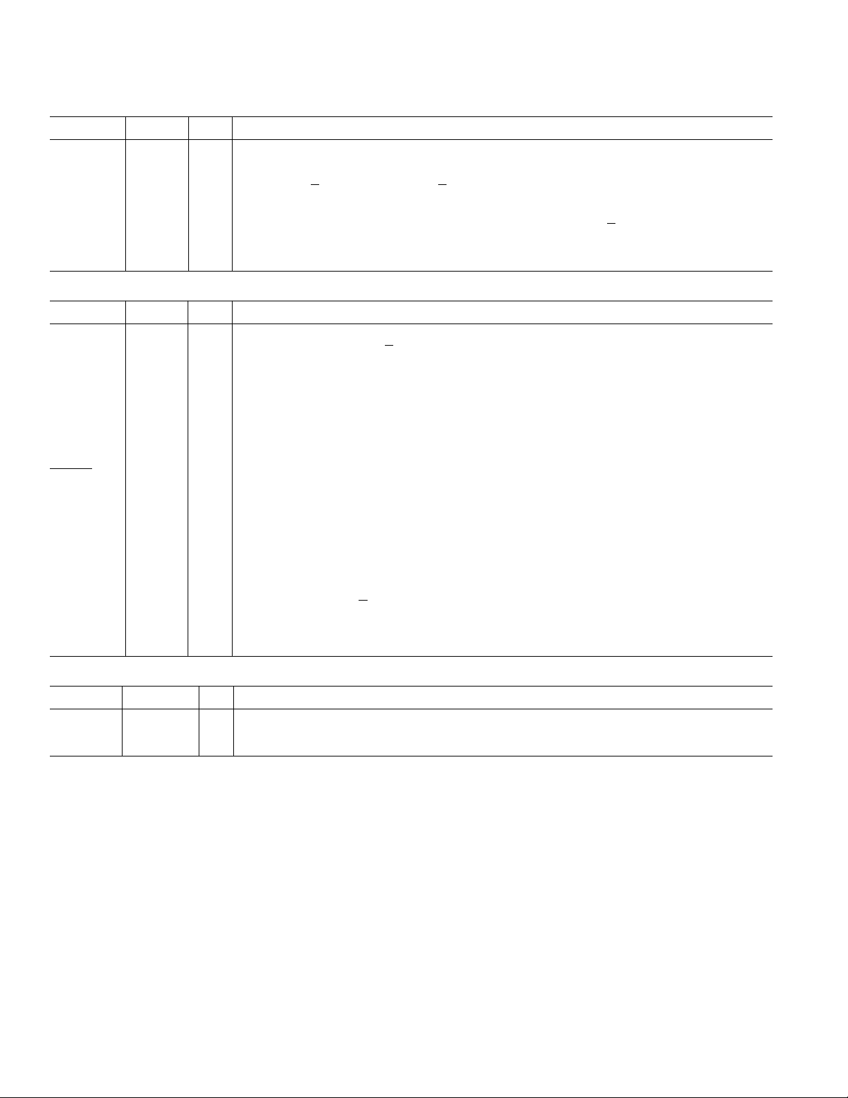
EXAMPLE
FREQUENCIES:
DAT 48kHz OR
CD 44.1kHz OR
BROADCAST 32kHz
AD1890/
AD1891
OUTPUT SAMPLE CLOCKINPUT SAMPLE CLOCK
INPUT SERIAL DATA
OUTPUT SERIAL DATA
EXAMPLE
FREQUENCIES:
DAT 48kHz OR
CD 44.1kHz OR
BROADCAST 32kHz
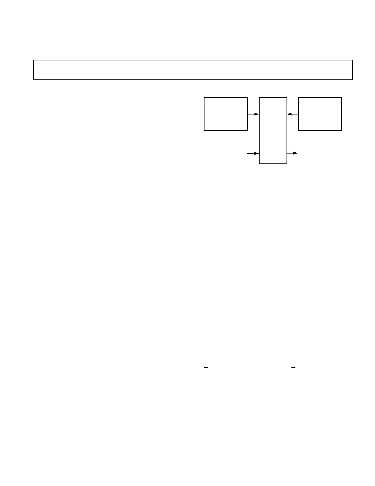
SamplePort Stereo Asynchronous
a
PRODUCT OVERVIEW
The AD1890 and AD1891 SamplePorts™ are fully digital, stereo
Asynchronous Sample Rate Converters (ASRCs) that solve sample
rate interfacing and compatibility problems in digital audio equipment. Conceptually, these converters interpolate the input data up
to a very high internal sample rate with a time resolution of 300 ps,
then decimate down to the desired output sample rate. The
AD1890 is intended for 18- and 20-bit professional applications,
and the AD1891 is intended for 16-bit lower cost applications
where large dynamic sample-rate changes are not encountered.
These devices are asynchronous because the frequency and phase
relationships between the input and output sample clocks (both are
inputs to the AD1890/AD1891 ASRCs) are arbitrary and need not
be related by a simple integer ratio. There is no need to explicitly
select or program the input and output sample clock frequencies, as
the AD1890/AD1891 automatically sense the relationship between
SamplePort and SamplePorts are trademarks of Analog Devices, Inc.
REV. 0
Information furnished by Analog Devices is believed to be accurate and
reliable. However, no responsibility is assumed by Analog Devices for its
use, nor for any infringements of patents or other rights of third parties
which may result from its use. No license is granted by implication or
otherwise under any patent or patent rights of Analog Devices.
FEATURES
Automatically Sense Sample Frequencies—No
Programming Required
Tolerant of Sample Clock Jitter
Smooth Transition When Sample Clock Frequencies
Cross
Accommodate Dynamically Changing Asynchronous
Sample Clocks
8 kHz to 56 kHz Sample Clock Frequency Range
1:2 to 2:1 Ratio Between Sample Clocks
–106 dB THD+N at 1 kHz (AD1890)
120 dB Dynamic Range (AD1890)
Optimal Clock Tracking Control
–Short/Long Group Delay Modes
–Slow/Fast Settling Modes
Linear Phase in All Modes
Equivalent of 4 Million 22-Bit FIR Filter Coefficients
Stored On-Chip
Automatic Output Mute
Flexible Four Wire Serial Interfaces
Low Power
APPLICATIONS
Digital Mixing Consoles and Digital Audio Workstations
CD-R, DAT, DCC and MD Recorders
Multitrack Digital Audio and Video Tape Recorders
Studio to Transmitter Links
Digital Audio Signal Routers/Switches
Digital Audio Broadcast Equipment
High Quality D/A Converters
Digital Tape Recorder Varispeed Applications
Computer Communication and Multimedia Systems
Sample Rate Converters
AD1890/AD1891
SYSTEM DIAGRAM
the two clocks. The input and output sample clock frequencies
can nominally range from 8 kHz to 56 kHz, and the ratio
between them can vary from 1:2 to 2:1.
The AD1890/AD1891 use multirate digital signal processing
techniques to construct an output sample stream from the input
sample stream. The input word width is 4 to 20 bits for the
AD1890 or 4 to 16 bits for the AD1891. Shorter input words
are automatically zero-filled in the LSBs. The output word
width for both devices is 24 bits. The user can receive as many
of the output bits as desired. Internal arithmetic is performed
with 22-bit coefficients and 27-bit accumulation. The digital
samples are processed with unity gain.
The input and output control signals allow for considerable flexibility for interfacing to a variety of DSP chips, AES/EBU
receivers and transmitters and for I
and output data can be independently justified to the left/right
clock edge, or delayed by one bit clock from the left/right clock
edge. Input and output data can also be independently justified
to the word clock rising edge or delayed by one bit clock from
the word clock rising edge. The bit clocks can also be independently configured for rising edge active or falling edge active
operation.
The AD1890/AD1891 SamplePort™ ASRCs have on-chip digital coefficients that correspond to a highly oversampled 0 kHz to
20 kHz low-pass filter with a flat passband, a very narrow transition band, and a high degree of stopband attenuation. A subset
of these filter coefficients are dynamically chosen on the basis of
the filtered instantaneous ratio between the input sample clock
(L
R_I) and the output sample clock (LR_O), and these coeffi-
cients are used in an FIR convolver to perform the sample rate
conversion. Refer to the “Theory of Operation” section of this
data sheet for a more thorough functional description. The lowpass filter has been designed so that full 20 kHz bandwidth is
maintained when the input and output sample clock frequencies
are as low as 44.1 kHz. If the output sample rate drops below
the input sample rate, the bandwidth of the input signal is
One Technology Way, P.O. Box 9106, Norwood, MA 02062-9106, U.S.A.
Tel: 617/329-4700 Fax: 617/326-8703
2
S compatible devices. Input
(continued on Page 4)

AD1890/AD1891–SPECIFICATIONS
TEST CONDITIONS UNLESS OTHERWISE NOTED
Supply Voltage +5.0 V
Ambient Temperature 25 °C
MCLK 20 MHz
Load Capacitance 100 pF
All minimums and maximums tested except as noted.
PERFORMANCE (Guaranteed over 0°C ≤ TA ≤ 70°C, VDD = 5.0 V ± 10%, 8 MHz ≤ MCLK ≤ 20 MHz)
Min Max Units
AD1890 Dynamic Range (20 Hz to 20 kHz, –60 dB Input)† 120 dB
AD1891 Dynamic Range (20 Hz to 20 kHz, –60 dB Input)† 96 dB
Total Harmonic Distortion + Noise† dB
AD1890 and AD1891 (20 Hz to 20 kHz, Full-Scale Input,
F
SOUT/FSIN
AD1890 (1 kHz Full-Scale Input, F
AD1890 (10 kHz Full-Scale Input, F
AD1891 (1 kHz Full-Scale Input, F
AD1891 (10 kHz Full-Scale Input, F
Interchannel Phase Deviation† 0 Degrees
Input and Output Sample Clock Jitter† 10 ns
(For ≤ 1 dB Degradation in THD+N with 10 kHz Full-Scale Input, Slow-Settling Mode)
Between 0.5 and 2.0) –94 dB
SOUT/FSIN
SOUT/FSIN
SOUT/FSIN
SOUT/FSIN
Between 0.7 and 1.4) –106 dB
Between 0.7 and 1.4) –100 dB
Between 0.7 and 1.4) –96 dB
Between 0.7 and 1.4) –95 dB
DIGITAL INPUTS (Guaranteed over 0°C ≤ TA ≤ 70°C, VDD = 5.0 V ± 10%, 8 MHz ≤ MCLK ≤ 20 MHz)
Min Max Units
V
IH
V
IL
I
@ VIH = +5 V 4 µA
IH
I
@ VIL = 0 V 4 µA
IL
V
@ IOH = –4 mA 3.6 V
OH
V
@ IOL = 4 mA 0.4 V
OL
2.2 V
0. 8 V
Input Capacitance† 15 pF
DIGITAL TIMING (Guaranteed over 0°C ≤ TA ≤ 70°C, VDD = 5.0 V ± 10%, 8 MHz ≤ MCLK ≤ 20 MHz)
Min Max Units
t
MCLK
f
MCLK
t
MPWL
t
MPWH
f
LRI
t
RPWL
t
RS
t
BCLK
f
BCLK
t
BPWL
t
BPWH
t
WSI
t
WSO
t
LRSI
t
LRSO
t
DS
t
DH
t
DPD
t
DOH
MCLK Period 50 125 ns
MCLK Frequency (1/t
) 8 20 MHz
MCLK
MCLK LO Pulse Width 20 ns
MCLK HI Pulse Width 20 ns
LR_I Frequency with 20 MHz MCLK† 10 70 kHz
RESET LO Pulse Width 100 ns
RESET Setup to MCLK Falling 15 ns
BCLK_I/O Period† 80 ns
BCLK_I/O Frequency (l/t
)† 12.5 MHz
BCLK
BCLK_I/O LO Pulse Width 40 ns
BCLK_I/O HI Pulse Width 40 ns
WCLK_I Setup to BCLK_I 15 ns
WCLK_O Setup to BCLK_O 30 ns
LR_I Setup to BCLK_I 15 ns
LR_O Setup to BCLK_O 30 ns
Data Setup to BCLK_I 0 ns
Data Hold from BCLK_I 25 ns
Data Propagation Delay from BCLK_O 40 ns
Data Output Hold from BCLK_O 5 ns
–2–
REV. 0
AD1890/AD1891
WARNING!
ESD SENSITIVE DEVICE
POWER (0°C ≤ TA ≤ 70°C, MCLK = 16 MHz, F
= 48 kHz, F
SIN
= 44.1 kHz)
SOUT
Min Typ Max Units
Supplies
Voltage, V
Current, I
Current, I
DD
(VDD = 5.0 V) 35 40 mA
DD
(VDD = 3.0 V) 19 mA
DD
2.7 5.5 V
Dissipation
Operation (V
= 5.0 V) 175 200 mW
DD
Operation (VDD = 3.0 V) 57 mW
TEMPERATURE RANGE
Min Max Units
Specifications Guaranteed 0 +70 °C
Operation Guaranteed –40 +85 °C
Storage –60 +100 °C
ABSOLUTE MAXIMUM RATINGS*
Min Max Units
V
to GND –0.3 7.0 V
DD
DC Input Voltage –0.3 V
+ 0.3 V
DD
Latch-Up Trigger Current –1000 +1000 mA
Soldering +300 °C
10 sec
*Stresses greater than those listed under “Absolute Maximum Ratings” may cause permanent damage to the device. This is a stress rating only and functional operation
of the device at these or any other conditions above those indicated in the operational section of this specification is not implied. Exposure to absolute maximum rating
conditions for extended periods may affect device reliability.
DIGITAL FILTER CHARACTERISTICS†
Min Max Units
Passband Ripple (0 to 20 kHz) 0.01 dB
Transition Band
1
4. 1 kHz
Stopband Attenuation 110 dB
Group Delay (LR–I = 50 kHz) 700 3000 µs
†Guaranteed. Not Tested
1
Valid only when F
Specifications subject to change without notice.
SOUT
≥ F
(i.e., upsampling), F
SIN
= 44.1 kHz.
SIN
ORDERING GUIDE
Model Temperature Range Package Description Package Option
AD1890JN 0°C to +70°C Plastic DIP N-28
AD1890JP 0°C to +70°C PLCC P-28A
AD1891JN 0°C to +70°C Plastic DIP N-28
AD1891JP 0°C to +70°C PLCC P-28A
CAUTION
ESD (electrostatic discharge) sensitive device. Electrostatic charges as high as 4000 V readily
accumulate on the human body and test equipment and can discharge without detection.
Although the AD1890/AD1891 features proprietary ESD protection circuitry, permanent
damage may occur on devices subjected to high energy electrostatic discharges. Therefore,
proper ESD precautions are recommended to avoid performance degradation or loss of
functionality.
REV. 0
–3–
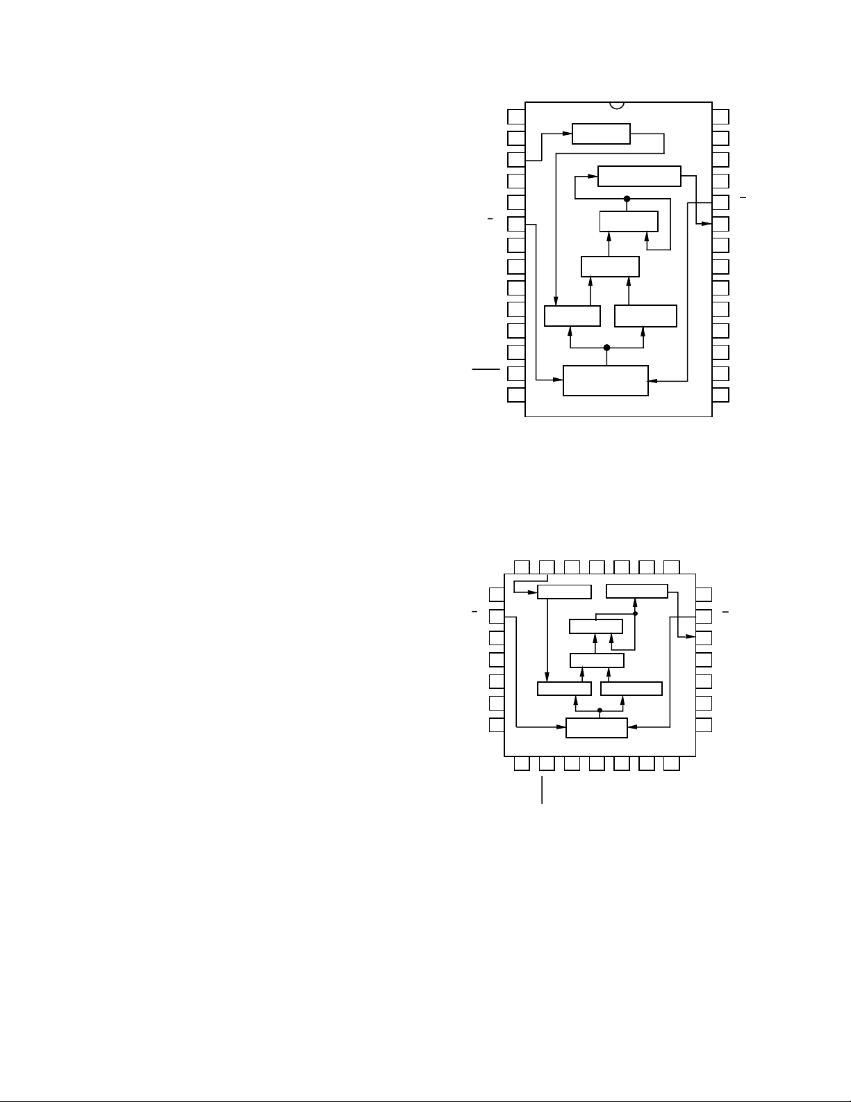
AD1890/AD1891
28
27
26
22
21
20
19
18
17
25
24
23
16
15
SERIAL IN
SERIAL OUT
MULT
CLOCK
TRACKING
ACCUM
RESET
LR_I
LR_O
1
2
3
7
8
9
10
11
12
4
5
6
13
14
COEF ROM
FIFO
GPDLYS (AD1890)
N/C (AD1891)
MCLK
DATA_I
BCLK_I
WCLK_I
V
DD
GND
N/C
BKPOL_I
TRGLR_I
MSBDLY_I
GND
SETSLW
GND
BCLK_O
WCLK_O
DATA_O
V
DD
GND
N/C
BKPOL_O
TRGLR_O
MSBDLY_O
MUTE_O
MUTE_I
AD1890/AD1891
N/C = NO CONNECT
22
21
20
19
25
24
23
7
8
9
10
11
5
6
LR_I
LR_O
SERIAL IN
RESET
SERIAL OUT
ACCUM
COEF ROM
FIFO
MULT
N/C
WCLK_I
V
DD
GND
BKPOL_I
TRGLR_I
WCLK_O
DATA_O
V
DD
GND
N/C
BKPOL_O
1234 282726
12 13 14 18171615
GPDLYS (AD1890)
N/C (AD1891)
MCLK
DATA_I
BCLK_I
SETLSLW
GND
BCLK_O
MSBDLY_I
GND
TRGLR_O
MSBDLY_O
MUTE_O
MUTE_I
CLOCK
TRACKING
AD1890/AD1891
N/C = NO CONNECT
(continued from Page 1)
PRODUCT OVERVIEW (Continued)
automatically limited to avoid alias distortion on the output signal. The AD1890/AD1891 dynamically alter the low-pass filter
cutoff frequency smoothly and slowly, so that real-time variations in the sample rate ratio are possible without degradation of
the audio quality.
The AD1890/AD1891 have a pin selectable slow- or fast-settling
mode. This mode determines how quickly the ASRCs adapt to a
change in either the input sample clock frequency (F
output sample clock frequency (F
mode, the control loop which computes the ratio between F
and F
jitter above 3 Hz. The slow-settling mode offers the best signal
quality and the greatest jitter rejection. In the fast-settling mode,
the control loop settles in approximately 200 ms and begins to
reject jitter above 12 Hz. The fast-settling mode allows rapid,
real time sample rate changes to be tracked without error, at the
expense of some narrow-band noise modulation products on the
output signal.
The AD1890 also has a pin selectable, short or long group delay
mode. This pin determines the depth of the First-In, First-Out
(FIFO) memory which buffers the input data samples before
they are processed by the FIR convolver. In the short mode, the
group delay is approximately 700 µs. The ASRC is more sensi-
tive to sample rate changes in this mode (i.e., the pointers which
manage the FIFO are more likely to cross and become momentarily invalid during a sample rate step change), but the group
delay is minimized. In the long mode, the group delay is approximately 3 ms. The ASRC is tolerant of large dynamic
sample rate changes in this mode, and it should be used when
the device is required to track fast sample rate changes, such as
in varispeed applications. The AD1891 features the short group
delay mode only. In either device, if the read and write pointers
that manage the FIFO cross (indicating underflow or overflow),
the ASRC asserts the mute output (MUTE_O) pin HI for 128
output clock cycles. If MUTE_O is connected to the mute input
(MUTE_I) pin, as it normally should be, the serial output will
be muted (i.e., all bits zero) during this transient event.
The AD1890/AD1891 are fabricated in a 0.8µm single poly,
double metal CMOS process and are packaged in a 0.6" wide
28-pin plastic DIP and a 28-pin PLCC. The AD1890/AD1891
operate from a +5 V power supply over the temperature range of
0°C to +70°C.
). In the slow-settling
SOUT
settles in approximately 800 ms and begins to reject
SOUT
SIN
) or the
SIN
–4–
AD1890/AD1891 DIP Pinout
AD1890/AD1891 PLCC Pinout
REV. 0
AD1890/AD1891
DEFINITIONS
Dynamic Range
The ratio of a near full-scale input signal to the integrated noise
in the passband (0 to ≈20 kHz), expressed in decibels (dB). Dynamic range is measured with a –60 dB input signal and
“60 dB” arithmetically added to the result.
Total Harmonic Distortion + Noise
Total Harmonic Distortion plus Noise (THD+N) is defined as
the ratio of the square root of the sum of the squares of the values of the harmonics and noise to the rms value of a sinusoidal
Group Delay
Intuitively, the time interval required for a full-level input pulse
to appear at the converter’s output, at full level, expressed in
milliseconds (ms). More precisely, the derivative of radian phase
with respect to radian frequency at a given frequency.
Transport Delay
The time interval between when an impulse is applied to the
converters input and when the output starts to be affected by
this impulse, expressed in milliseconds (ms). Transport delay is
independent of frequency.
input signal. It is usually expressed in percent (%) or decibels.
Interchannel Phase Deviation
Difference in input sampling times between stereo channels, expressed as a phase difference in degrees between 1 kHz inputs.
AD1890/AD1891 PIN LIST
Serial Input Interface
Pin Name Number I/O Description
DATA_I 3 I Serial input, MSB first, containing two channels of 4- to 20-bits of twos-complement data per
channel. AD1891 ONLY: Maximum of 16 data bits per channel; additional bits ignored.
BCLK_I 4 I Bit clock input for input data.
WCLK_I 5 I Word clock input for input data. This input is rising edge sensitive. (Not required in L
R input data
clock triggered mode [TRGLR_I = HI].)
LR_I 6 I Left/right clock input for input data. Must run continuously.
Serial Output Interface
Pin Name Number I/O Description
DATA_O 23 O Serial output, MSB first, containing two channels of 4- to 24-bits of twos-complement data per
channel.
BCLK_O 26 I Bit clock input for output data.
WCLK_O 25 I Word clock input for output data. This input is rising edge sensitive. (Not required in L
R output
data clock triggered mode [TRGLR_O = HI].)
LR_O 24 I Left/right clock input for output data. Must run continuously.
Input Control Signals
Pin Name Number I/O Description
BKPOL_I 10 I Bit clock polarity. LO: Normal mode. Input data is sampled on rising edges of BCLK_I. HI:
Inverted mode. Input data is sampled on falling edges of BCLK_I.
TRGLR_I 11 I Trigger on L
R_I. HI: Changes in LR_I indicate beginning1 of valid input data. LO: Rising edge of
WCLK_I indicates beginning of valid input data.
MSBDLY_I 12 I MSB delay. HI: Input data is delayed one BCLK_I after either L
(TRGLR_I = LO) indicates the beginning of valid input data. Included for I
R_I (TRGLR_I = HI) or WCLK_I
2
S data format
compatibility. LO: No delay.
NOTE
1
The beginning of valid data will be delayed by one BLCK_I if MSBDEL_I is selected (HI).
REV. 0
–5–
AD1890/AD1891
Output Control Signals
Pin Name Number I/O Description
BKPOL_O 19 I Bit clock polarity. LO: Normal mode. Output data is valid on rising edges of BCLK_O, changed
on falling. HI: Inverted mode. Output data is valid on falling edges of BCLK_O, changed on rising.
TRGLR_O 18 I Trigger on L
edge of WCLK_O indicates beginning of valid output data.
R_O. HI: Changes in LR_O indicate beginning1 of valid output data. LO: Rising
MSBDLY_O 17 I MSB delay. HI: Output data is delayed one BCLK_O after either L
WCLK_O (TRGLR_O = LO) indicates the beginning of valid output data. Included for I
R_O (TRGLR_O = HI) or
2
S data
format compatibility. LO: No delay.
Miscellaneous
Pin Name Number I/O Description
GPDLYS 1 I AD1890 ONLY: Group delay—short. HI: Short group delay mode (≈700 µs). More sensitive to
changes in sample rates (L
R clocks). LO: Long group delay mode (≈3 ms). More tolerant of
sample rate changes. This signal may be asynchronous with respect to MCLK, and dynamically
changed, but is normally pulled up or pulled down on a static basis. AD1891: Short group delay
mode only; this pin is a N/C.
MCLK 2 I Master clock input. Nominally 16 MHz for sampling frequencies (F
, word rates) from 8 kHz to
S
56 kHz. Exact frequency is not critical, and does not need to be synchronized to any other clock
or possess low jitter.
RESET 13 I Active LO reset. Set HI for normal chip operation.
MUTE_O 16 O Mute output. HI indicates that data is not currently valid due to read and write FIFO memory
pointer overlap. LO indicates normal operation.
MUTE_I 15 I Mute input. HI mutes the serial output to zeros (midscale). Normally connected to MUTE_O.
Reset LO for normal operation.
SETLSLW 28 I Settle slowly to changes in sample rates. HI: Slow-settling mode (≈800 ms). Less sensitive to
sample clock jitter. LO: Fast-settling mode (≈200 ms). Some narrow-band noise modulation may
result from jitter on L
R clocks. This signal may be asynchronous with respect to MCLK, and
dynamically changed, but is normally pulled up or pulled down on a static basis.
N/C 9, 20 No connect. Reserved. Do not connect.
Power Supply Connections
Pin Name Number I/O Description
V
DD
7, 22 I Positive digital voltage supply.
GND 8, 14, 21, 27 I Digital ground. Pins 14 and 27 need not be decoupled.
NOTE
1
The beginning of valid data will be delayed by one BCLK_O if MSBDEL _O is selected (Hl).
–6–
REV. 0

AD1890/AD1891
THEORY OF OPERATION
There are at least two logically equivalent methods of explaining
the concept of asynchronous sample rate conversion: the high
speed interpolation/decimation model and the polyphase filter
bank model. Using the AD1890 and AD1891 SamplePorts does
not require understanding either model. This section is included
for those who wish a deeper understanding of their operation.
Interpolation/Decimation Model
In the high speed interpolation/decimation model, illustrated in
Figure 1, the sampled data input signal (Plot A in Figure 1) is
interpolated at some ratio (IRATIO) by inserting IRATIO-1
zero valued samples between each of the original input signal
samples (Plot B in Figure 1). The frequency domain characteristics of the input signal are unaltered by this operation, except
that the zero-padded sequence is considered to be sampled at a
frequency which is the product of original sampling frequency
multiplied by IRATIO.
The zero-padded values are fed into a digital FIR low-pass filter
(Plot C in Figure 1) to smooth or integrate the sequence, and
limit the bandwidth of the filter output to 20 kHz. The interpolated output signal has been quantized to a much finer time
scale than the original sequence. The interpolated sequence is
then passed to a zero-order hold functional block (physically
INPUT
SIGNAL
A
ZERO STUFF
INTERPOLATION
AMP
A
BC
FIR LOW
PASS
FILTER
implemented as a register, Plot D in Figure 1) and then asynchronously resampled at the output sample frequency (Plot E in
Figure 1). This resampling can be thought of as a decimation
operation since only a very few samples out of the great many
interpolated samples are retained. The output values represent
the “nearest” values, in a temporal sense, produced by the interpolation operation. There is always some error in the output
sample amplitude due to the fact that the output sampling
switch does not close at a time that exactly corresponds to a
point on the fine time scale of the interpolated sequence. However, this error can be made arbitrarily small by using a very
large interpolation ratio. The AD1890/AD1891 SamplePort
ASRCs use an equivalent IRATIO of 65,536 to provide 16-bit
accuracy (≈ –96 dB THD+N) across the 0 to 20 kHz audio
band.
The number of FIR filter taps and associated coefficients is
approximately 4 million. The equivalent FIR filter convolution
frequency (or “upsample” frequency) is 3.2768 GHz, and the
fine time scale has resolution of about 300 ps. Various proprietary efficiencies are exploited in the AD1890/AD1891 ASRCs
to reduce the complexity and throughput requirements of the
hardware implied by this interpolation/decimation model.
ZERO ORDER
HOLD
REGISTER
DE
RESAMPLING
DECIMATION
TIME
OUTPUT
SIGNAL
B
C
D
E
Figure 1. Interpolation/Decimation Model—Time Domain View
REV. 0
–7–

AD1890/AD1891
Polyphase Filter Bank Model
Although less intuitively understandable than the interpolation/
decimation model, the polyphase filter bank model is useful to
explore because it more accurately portrays the operation of the
actual AD1890/AD1891 SamplePort hardware. In the polyphase
filter bank model, the stored FIR filter coefficients are thought
of as the impulse response of a highly oversampled 0 to 20 kHz
low-pass prototype filter, as shown in Figure 2. If this low-pass
filter is oversampled by a factor of N, then it can be conceptually decomposed into N different “subfilters,” each filter consisting of a different subset of the original set of impulse response
samples. If the temporal position of each of the subfilters is
maintained, then they can be summed to recreate the original
oversampled impulse response. Since the original impulse
response is highly oversampled, the more sparsely sampled
subfilters still individually meet the Nyquist criterion (i.e., they
OVERSAMPLED
LOW PASS FILTER
AMP
IMPULSE RESPONSE
TIME
are adequately sampled). The baseband magnitude and phase
responses of the subfilters are identical. The out-of-band (i.e.,
alias) regions of the subfilters however have phase responses
which are shifted relative to one another, in a manner that
causes them to cancel when they are summed.
The subfilter coefficients are then aligned to the left, as shown
in Figure 3, so that the first coefficient of each subfilter is
aligned to the first point on a coarse time scale. (This conceptual step accounts for how the hardware implementation is able
to operate at the slower rate corresponding to the coarse time
scale.) Each subfilter has been shifted in time by a different
amount, and though they still share identical magnitude
responses, they now have in-band phase responses which have
fractionally different slopes (i.e., group delays).
PHASE
90
0 Deg
180
AMP
1/4Fs 1/2Fs 3/4Fs Fs
270
FREQ
DECOMPOSED INTO
FOUR SUBFILTERS
1/4Fs 1/2Fs 3/4Fs Fs
1/4Fs 1/2Fs 3/4Fs Fs
1/4Fs 1/2Fs 3/4Fs Fs
1/4Fs 1/2Fs 3/4Fs Fs
Figure 2. Four Polyphase Subfilters in the Time and Frequency Domains
–8–
REV. 0

AD1890/AD1891
AMP
SUBFILTER COEFFICIENTS
ALIGNED TO THE LEFT
T
= 1/F
sin
sin
TIME
PHASE
F
/2
sin
DELAY = NOMINAL
F
/2
sin
DELAY = NOMINAL
F
/2
sin
DELAY = NOMINAL – .25/F
F
/2
sin
DELAY = NOMINAL – .5/F
F
/2
sin
FREQ
sin
sin
Figure 3. Four Polyphase Subfilters Realigned to Coarse Time Grid
PARALLEL POLYPHASE
FILTER BANK
POLYPHASE FILTER 1
POLYPHASE FILTER 2
POLYPHASE FILTER 3
POLYPHASE FILTER 4
POLYPHASE FILTER 5
INPUT
SIGNAL
POLYPHASE FILTER 6
POLYPHASE FILTER 7
POLYPHASE FILTER N-1
POLYPHASE FILTER N
N TO 1
MUX
SELECT
SAMPLE
CLOCK
TRACKING
CIRCUIT
OUTPUT
SIGNAL
Figure 4. Polyphase Filter Bank Model—Conceptual Block
Diagram
DELAY = NOMINAL – .75/F
sin
The full set of subfilters can be considered to form a parallel
bank of “polyphase” filters which have decrementing, linear
phase group delays. All of the polyphase filters conceptually process the input signal simultaneously, as illustrated in Figure 4, at
the input sample rate.
REV. 0
–9–

AD1890/AD1891
Asynchronous sample rate conversion under the polyphase filter
bank model is accomplished by selecting the output of a particular polyphase filter on the basis of the temporal relationship between the input sample clock and the output sample clock
events. Figure 5 shows the desired filter group delay as a function of the relative time difference between the current output
sample clock and the last input sample clock. If an output
sample is requested late in the input sample period, then a short
filter delay is required, and if an output sample is requested
early in the input sample period, then a long filter delay is required. This nonintuitive result arises from the fact that FIR filters always produce some delay, so that selecting a filter with
shorter delay moves the interpolated sample closer to the newest
input sample.
A short delay corresponds to a large offset into the dense FIR
filter coefficient array, and a long delay corresponds to a small
offset. Note that because the output sample clock can arrive at
any arbitrary time with respect to the input sample clock, the
selection of a polyphase filter with which to convolve the input
sequence occurs on every output sample clock event. Occasionally the FIFO which holds the input sequence in the FIR convolver is either not incremented, or incremented by two between
output sample clocks (see periods A and B in Figure 5); this
happens more often when the input and output sample clock
frequencies are dissimilar than when they are close together.
However, in this situation, an appropriate polyphase filter is
selected to process the input signal, and thus an accurate output
sample is computed. Input and output samples are not skipped
or repeated (unless the input FIFO underflows or overflows), as
is the case in some other sample rate converter implementations.
To obtain an accurate conversion, a large number of polyphase
filters are needed. The AD1890/AD1891 SamplePorts use the
equivalent of 65,536 polyphase filters to achieve their professional audio quality distortion and dynamic range specifications.
Sample Clock Tracking
It should be clear that, in either model, the correct computation
of the ratio between the input sample rate (as determined from
the left/
right input clock, LR_I) and the output sample rate (as
determined from the left/
right output clock, LR_O) is critical to
the quality of the output data stream. It is straightforward to
compute this ratio if the sample rates are fixed and synchronous;
the challenge is to accurately track dynamically varying and
asynchronous sample rates, as well as to account for jitter.
WCLK_I
DATA_I
BCLK_I
SERIAL DATA
INPUT UNIT
LR_I
GENERATOR
LARGE
OFFSET
SMALL
OFFSET INTO DENSE FIR FILTER COEFFICIENT ARRAY
TO ACCESS REQUIRED POLYPHASE FILTER
REQUIRED FILTER GROUP DELAY TO
COMPUTE REQUESTED OUTPUT SAMPLE
AB
INPUT SEQUENCE
PAST
OUTPUT SEQUENCE
OFFSET
LONG
DELAY
SHORT
DELAY
AMPLITUDE
AMPLITUDE
FUTURE
Figure 5. Input and Output Clock Event Relationship
The AD1890/AD1891 SamplePorts solve this problem by
embedding the ratio computation circuit within a digital servo
control loop, as shown in Figure 6. This control loop includes
special provisions, to allow for the accurate tracking of dynamically changing sample rates. The outputs of the control loop are
the starting read addresses for the input data FIFO and the filter
coefficient ROM. These start addresses are used by the FIFO
and ROM address generators, as shown in Figure 6.
The input data FIFO write address is generated by a counter
which is clocked by the input sample clock (i.e., L
R_I). It is very
important that the FIFO read address and the FIFO write address do not cross, as this means that the FIFO has either
underflowed or overflowed. This consideration affects the
choice of settling time of the control loop. When a step change
in the sample rate occurs, the relative positions of the read and
write addresses will change while the loop is settling. A fast settling loop will act to keep the FIFO read and write addresses
separated better than a slow settling loop. The AD1890/
AD1891 include a user selectable pin (SETLSLW) to set the
loop settling time that essentially changes the coefficients of the
digital servo control loop filter. The state of the SETLSLW pin
can be changed on-the-fly but is normally set and forgotten.
LR_I
FIFO WRITE
ADDRESS
SAMPLE CLOCK RATIO
SERVO CONTROL LOOP
LR_I
(F
)
SIN
LR_O
(F
SOUT
FIFO READ
ADDRESS
START
ADDRESS
)
GENERATOR
POLYPHASE FILTER
SELECTOR
ROM ADDRESS
GENERATOR
F
< F
SOUT
SIN
FREQUENCY
RESPONSE
COMPRESSION
LR_I LR_O
FIFO
POLYPHASE
COEFFICIENT
ROM
ACCUMULATOR
FIR CONVOLVER
BCLK_O
SERIAL DATA
OUTPUT UNIT
WCLK_O
LR_O
DATA_O
Figure 6. AD1890/AD1891 Functional Block Diagram
–10–
REV. 0

AD1890/AD1891
Sample Clock Jitter Rejection
The loop filter settling time also affects the ability of the
AD1890/AD1891 ASRCs to reject sample clock jitter, since the
control loop effectively computes a time weighted average or
“estimated” new output of many past input and output clock
events. This first order low pass filtering of the sample clock
ratio provide the AD1890/AD1891 with their jitter rejection
characteristic. In the slow settling mode, the AD1890/AD1891
attenuate jitter frequencies higher than 3 Hz (≈800 ms for the
control loop to settle to an 18-bit “pure” sine wave), and thus
reject all but the most severe sample clock jitter; performance is
essentially limited only by the FIR filter. In the fast settling
mode, the ASRCs attenuate jitter components above 12 Hz
(≈200 ms for the control loop to settle). Due to the effects of
on-chip synchronization of the sample clocks to the 16 MHz
(62.5 ns) MCLK master clock, sample clock jitter must be a
large percentage of the MCLK period (>10 ns) before performance degrades in either the slow or fast settling modes. Note
that since both past input and past output clocks are used to
compute the filtered “current” internal output clock request, jitter on both the input sample clock and the output sample clock
is rejected equally. In summary: the fast settling mode is best for
applications when the sample rates will be dynamically altered
(e.g., varispeed situations) while the slow settling mode provides
the most sample clock jitter rejection.
Clock jitter can be modeled as a frequency modulation process.
Figure 7 shows one such model, where a noise source combined
with a sine wave source modulates the “carrier” frequency generated by a voltage controlled oscillator.
NOISE SOURCE
NOISE
WAVEFORM
SINE
WAVE
Σ
VOLTAGE
SOURCE
Figure 7. Clock Jitter Modeled as a Modulated VCO
ANALOG IN
VCO
ADC
DIGITAL
OUT
If the jittered output of the VCO is used to clock an analog-todigital converter, the digital output of the ADC will be contaminated by the presence of jitter. If the noise source is spectrally
flat (i.e., “white” jitter), then an FFT of the ADC digital output
would show a spectrum with a uniform noise floor which is elevated compared to the spectrum with the noise source turned
off. If the noise source has distinct frequency components (i.e.,
“correlated” jitter), then an FFT of the ADC digital output
would show symmetrical sidebands around the ADC input signal, at amplitudes and frequencies determined by frequency
modulation theory. One notable result is that the level of the
noise or the sidebands is proportional to the slope of the input
signal, i.e., the worst case occurs at the highest frequency fullscale input (a full-scale 20 kHz sinusoid).
The AD1890/AD1891 apply rejection to these jitter frequency
components referenced to the input signal. In other words, if a
5 kHz digital sinusoid is applied to the ASRC, depending on the
settling mode selected, the ASRC will attenuate sample clock
jitter at either 3 Hz above and below 5 kHz (slow settling) or
12 Hz above and below 5 kHz (fast settling). The rolloff is 6 dB
per octave. As an example, suppose there was correlated jitter
present on the input sample clock with a 1 kHz component,
associated with the same 5 kHz sinusoidal input data. This
would produce sidebands at 4 kHz and 6 kHz, 3 kHz and
7 kHz, etc., with amplitudes that decrease as they move away
from the input signal frequency. For the slow settling mode
case, 1 kHz represents more than nine octaves (relative to
3 Hz), so the first two sideband pairs would be attenuated by
more than 54 dB. For the fast settling mode case, 1 kHz represents more than seven octaves (relative to 12 Hz), so that the
first two sideband pairs would be attenuated by more than
42 dB. The second and higher sideband pairs are attenuated
even more because they are spaced further from the input signal
frequency.
Group Delay Modes
The other parameter that determines the likelihood of FIFO input overflow or output underflow is the FIFO depth. This is the
parameter that is selected by the GPDLYS pin (AD1890 only;
this pin is a No Connect for the AD1891). The drawback with
increasing the FIFO depth is increasing the device’s overall
group delay, but most applications are insensitive to a small increase in group delay. [This FIFO-induced group delay is better
termed transport delay, since it is frequency independent, and
should be kept conceptually distinct from the notion of group
delay as used in the polyphase filter bank model. The total
group delay of the AD1890/AD1891 equals the FIFO transport
delay plus the FIR (polyphase) filter group delay.]
In the short group delay mode, the FIFO read and write pointers are separated by five memory locations (≈100 µs equivalent
transport delay at a 50 kHz sample rate). This is added to the
FIR filter delay (64 taps divided by 2) for a total nominal group
delay in short mode of ≈700 µs. The short group delay mode is
useful when the input and output sample clocks are asynchronous but either do not vary or change very slowly.
In the long group delay mode (AD1890 only, the AD1891 is
always in the short group delay mode), the FIFO read and write
pointers are separated by 96 memory locations (≈2 ms equivalent transport delay). This is added to the FIR filter delay
(64 taps divided by 2) for a total nominal group delay in long
mode of ≈3 ms. The long group delay mode is useful when the
input and output sample clocks are asynchronous and changing
relative to one another, such as during varispeed effects.
These delays are deterministic and constant except when F
drops below F
which causes the number of FIR filter taps to
SIN
SOUT
increase (see “Cutoff Frequency Modification” below). In either
mode, if the FIFO read and write addresses cross, the MUTE_O
signal will be asserted. Note that in all modes and under all conditions, both the highly oversampled low-pass prototype and the
polyphase subfilters of the AD1890/AD1891 ASRCs possess a
linear phase response.
The AD1890 has been designed so that when it is in long group
delay mode and fast settling mode, a full 2:1 step change (i.e.,
occurring between two samples) in sample frequency ratio can
be tolerated without output mute.
REV. 0
–11–

AD1890/AD1891
0.5 1.0 1.5 2.0
NUMBER OF FILTER TAPS
128
64
F
SOUT/FSIN
UPSAMPLING
DOWN-
SAMPLING
Cutoff Frequency Modification
The final important operating concept of the ASRCs is the modification of the filter cutoff frequency when the output sample
rate (F
) drops below the input sample rate (F
SOUT
SIN
), i.e.,
during downsampling operation. The AD1890/AD1891 automatically reduces the polyphase filter cutoff frequency under
this condition. This lowering of the cutoff frequency (i.e., the
reduction of the input signal bandwidth) is required to avoid
alias distortion. The AD1890/AD1891 SoundPorts take advantage of the scaling property of the Fourier transform which can
be stated as follows: if the Fourier transform of f(t) is F(w), then
the Fourier transform of f(k × t) is F(w/k). This property can be
used to linearly compress the frequency response of the filter,
simply by multiplying the coefficient ROM addresses (shown in
Figure 6) by the ratio of F
than F
. This scaling property works without spectral distor-
SIN
SOUT
to F
whenever F
SIN
SOUT
is less
tion because the time scale of the interpolated signal is so dense
(300 ps resolution) with respect to the cutoff frequency that the
discrete-time representation is a close approximation to the continuous time function.
The cutoff frequency (–3 dB down) of the FIR filter during
downsampling is given by the following relation:
Downsampling Cutoff Frequency = (F
/44.1 kHz) × 20 kHz
SOUT
The AD1890/AD1891 frequency response compression circuit
includes a first order low-pass filter to smooth the filter cutoff
frequency selection during dynamic sample rate conditions.
This allows the ASRC to avoid objectionable clicking sounds
that would otherwise be imposed on the output while the loop
settles to a new sample rate ratio. Hysteresis is also applied to
the filter selection with approximately 300 Hz of cutoff frequency “noise margin,” which limits the available selection of
cutoff frequencies to those falling on an approximately 300 Hz
frequency grid. Thus if a particular sample frequency ratio was
reached by sliding the output sample frequency up, it is possible
that a filter will be chosen with a cutoff frequency that could differ by as much as 300 Hz from the filter chosen when the same
sample frequency ratio was reached by sliding the output sample
frequency down. This is necessary to ensure that the filter selection is stable even with severely jittered input sample clocks.
Note that when the filter cutoff frequency is reduced, the transition band of the filter becomes narrower since the scaling property affects all filter characteristics. The number of FIR filter
taps necessarily increases because there are now a smaller number of longer length polyphase filters. Nominally, when F
greater than F
than F
SIN,
128 when the ratio of F
, the number of taps is 64. When F
SIN
SOUT
the number of taps linearly increase to a maximum of
SOUT
, to F
equals 1:2. The number of
SIN
SOUT
is less
is
filter taps as a function of sample clock ratio is illustrated in Figure 8. The natural consequence of this increase in filter taps is
an increase in group delay.
When the AD1890/AD1891 output sample frequency is higher
than the input sample frequency (i.e., upsampling operation),
the cutoff frequency of the FIR polyphase filter can be greater
than 20 kHz. The cutoff frequency of the FIR filter during
upsampling is given by the following relation:
Upsampling Cutoff Frequency = (F
/44.1 kHz) × 20 kHz
SIN
Noise and Distortion Phenomena
There are three noise/distortion phenomena that limit the performance of the AD1890/AD1891 ASRCs. First, there is
Figure 8. Number of Filter Taps as a Function of
F
SOUT/FSlN
broadband, Gaussian noise which results from polyphase filter
selection quantization. Even though the AD1890/AD1891 have
a large number of polyphase filters (the equivalent of 65,536) to
choose from, the selection is not infinite. Second, there is
narrow-band noise which results from the non-ideal synchronization of the sample clocks to the system clock MCLK, which
leads to a non-ideal computation of the sample clock ratio,
which leads to a non-ideal polyphase filter selection. This noise
source is narrowband because the digital servo control loop
averages the polyphase filter selection, leading to a strong correlation between selections from output to output. In slow mode,
the selection of polyphase filters is completely unaffected by the
clock synchronization. In fast mode, some narrowband noise
modulation may be observed with very long FFT measurements. This situation is analogous to the behavior of a phase
locked loop when presented with a noisy or jittered input.
Third, there are distortion components that are due to the
non-infinite stopband rejection of the low-pass filter response.
Non-infinite stopband rejection means that some amount of
out-of-band spectral energy will alias into the baseband. The
AD1890/AD1891 performance specifications include the effects
of these phenomena.
Note that Figures 15 through 17 are shown with full-scale input
signals. The distortion and noise components will scale with the
input signal amplitude. In other words, if the input signal is attenuated by –20 dB, the distortion and noise components will
also be attenuated by –20 dB. This dependency holds until the
effects of the 20-bit input quantization are reached.
–12–
REV. 0

AD1890/AD1891
OPERATING FEATURES
Serial Input/Output Ports
The AD1890/AD1891 use the frequency of the left/right input
clock (L
R_I) and the left/right output clock (LR _O) signals to
determine the sample rate ratio, and therefore these signals must
run continuously and transition twice per sample period. (The
L
R_I clock frequency is equivalent to F
frequency is equivalent to F
.) The other clocks (WCLK_I,
SOUT
and the LR_O clock
SIN
WCLK_O, BCLK_I, BCLK_O) are edge sensitive and may be
used in a gated or burst mode (i.e., a stream of pulses during
data transmission or reception followed by periods of inactivity).
The word clocks and bit clocks are used only to write data into
or read data out of the serial ports; only the left/
right clocks are
used in the internal DSP blocks. It is important that the left/
right clocks are “clean” with monotonic rising and falling edge
transitions and no excessive overshoot or undershoot which
could cause false triggering on the AD1890/AD1891.
The AD1890/AD1891’s flexible serial input and output ports
consume and produce data in twos-complement, MSB-first
format. The left channel data field always precedes the right
channel data field; the current channel being consumed or produced is indicated by the state of the left/
L
R_O). A left channel field, right channel field pair is called a
right clock (LR_I and
frame. The input data field consists of 4 to 20 bits for the
AD1890, and 4 to 16 bits for the AD1891. The output data
field consists of 4 to 24 bits for both devices. The input signals
are specified to TTL logic levels, and the outputs swing to full
CMOS logic levels. The ports are configured by pin selections.
Serial I/O Port Modes
The AD1890/AD1891 has pin-selectable bit clock polarity for
the input and output ports. In “normal” mode (BKPOL_I or
BKPOL_O LO) the data is valid on the rising edge. In the
“inverted” mode (BKPOL_I or BKPOL_O HI) the data is
valid on the falling edge. Both modes are shown in Figures 22
and 23.
In the pin selectable MSB delay mode, which can be set independently for the input and output ports, the MSB is delayed by
one bit clock. This is useful for I
2
S format compatibility and for
ease of interfacing to some DSP processors. Both the MSB delay mode (MSBDLY_I or MSBDLY_O HI) and the MSB
non-delay mode (MSBDLY_I or MSBDLY_O LO) are shown
in Figures 22 and 23.
The AD1890/AD1891 SamplePort serial ports operate in either
the word clock (WCLK_I, WCLK_O) triggered mode or left/
right clock (LR_I, LR_O) triggered mode. These modes can be
utilized independently for the input and output ports, by resetting or setting the TRGLR_I and TRGLR_O control lines
respectively. In the word clock triggered mode, as shown in Figure 22, after the left/
right clock is valid, the appearance of the
MSB of data is synchronous with the rising edge of the word
clock (or delayed by one bit clock if the MSB delay mode is
selected). Note that the word clock is rising edge sensitive, and
can fall anytime after it is sampled HI by the bit clock. In the
left/
right clock triggered mode, as shown in Figure 23, the
appearance of the MSB of data is synchronous with the rising
edge of the left/
edge of left/
delayed by one bit clock after the left/
right clock for the left channel and the falling
right clock for the right channel. The MSB is
right clock if the MSB
delay mode is selected. The word clock is not required in the
left/
right clock triggered mode, and should be tied either HI or
LO. Figure 23 shows the bit clock in the optional gated or burst
mode; the bit clock is inactive between data fields, and can take
either the HI state or the LO state while inactive.
Note that there is no requirement for a delay between the left
channel data and the right channel data. The left/
right clocks
and the word clocks can transition immediately after the LSB of
the data, so that the MSB of the subsequent channel appears
without any timing delay. The AD1891 is therefore capable of a
32-bit frame mode, in which both 16-bit channels are packed
into a 32-bit clock period. More generally, there is no particular
requirement for when the left/
left/
right clock duty cycle or pulse width specification), provided
that the left/
right clock frequency equals the intended sample
right clock falls (i.e., there is no
frequency, and there are sufficient bit clock periods to clock in
or out the intended number of data bits.
Control Signals
The GPDLYS, SETLSLW, BKPOL_I, BKPOL_O, TRGLR_I,
TRGLR_O, MSBDLY_I, and MSBDLY_O inputs are asynchronous signals in that they need obey no particular timing
relation to MCLK or the sample clocks. Ordinarily, these pins
are hardwired or connected to an I/O register for microprocessor
control. The only timing requirement on these pins is that the
control signals are stable and valid before the first serial input
data bit (i.e., the MSB) is presented to the AD1890/AD1891.
Reset
Figure 25 shows the reset timing for the AD1890/AD1891
SamplePorts. MCLK must be running when
asserted, and the bit clocks, the word clocks and the left/
RESET is
right
clocks may also be running. When the AD1890/AD1891 come
out of reset, they default to a F
SIN
to F
ratio of 1:1. The fil-
SOUT
ter pipeline is not cleared. However, the mute output goes HI
for at least 128 cycles, adequate to allow the pipeline to clear. If
F
differs significantly from F
SIN
, then the AD1890/AD1891
SOUT
sample clock servo control loop also has to settle. While settling,
the mute output will be HI. After the external system resets the
AD1890/AD1891, it should wait until the mute output goes LO
before clocking in serial data.
There is no requirement for using the
RESET pin at power-up
or when the input or output sample rate changes. If it is not
used, the AD1890/AD1891 will settle to the sample clocks supplied within ≈200 ms in fast-settling mode or within ≈800 ms in
slow-settling mode.
REV. 0
–13–

80
0
80
24
8
8
16
0
48
32
40
56
64
72
7264564840322416
F
sin
– kHz
F
sout
– kHz
70kHz
F
sin/Fsout
= 2/1
F
sin/Fsout
= 1/1F
sin/Fsout
= 1/2
10kHz
70kHz
UPSAMPLING
DOWNSAMPLING
80
0
80
24
8
8
16
0
48
32
40
56
64
72
7264564840322416
F
sin
– kHz
F
sout
– kHz
56kHz
F
sin/Fsout
= 2/1
F
sin/Fsout
= 1/1F
sin/Fsout
= 1/2
8kHz
56kHz
DOWNSAMPLING
UPSAMPLING
80
0
80
24
8
8
16
0
48
32
40
56
64
72
7264564840322416
F
sin
– kHz
F
sout
– kHz
42kHz
F
sin/Fsout
= 2/1
F
sin/Fsout
= 1/1F
sin/Fsout
= 1/2
6kHz
42kHz
UP-
SAMPLING
DOWN-
SAMPLING
AD1890/AD1891
APPLICATION ISSUES
Dither
Due to the large output word length, no redithering of the
AD1890/AD1891 output is necessary. This assumes that the
input is properly dithered and the user retains the same or
greater number of output bits as there are input bits. The
AD1890/AD1891 output bit stream may thus be used directly
as the input to downstream digital audio processors, storage
media or output devices.
If the AD1890/AD1891 is to be used to dramatically downsample (i.e., output sample frequency is much lower than input
sample frequency), the input should be sufficiently dithered to
account for the limiting of the input signal bandwidth (which
reduces the RMS level of the input dither). No dither is internally used or applied to the audio data in the AD1890/AD1891
SamplePorts.
Decoupling and PCB Layout
The AD1890/AD1891 ASRCs have two power (Pins 7 and 22)
and two ground (Pins 8 and 21) connections to minimize output
switching noise and ground bounce. [Pins 14 and 27 are actually control inputs, and should be tied LO, but need not be
decoupled.] The DIP version places these pins at the center of
the device to optimize switching performance. The AD1890/
AD1891 should be decoupled with two high quality 0.1µF or
0.01 µF ceramic capacitors (preferably surface mount chip
capacitors, due to their low inductance), one between each V
GND pair. Best practice PCB layout and interconnect guidelines should be followed. This may include terminating MCLK
or the bit clocks if excessive overshoot or undershoot is evident
and avoiding parallel PCB traces to minimize digital crosstalk
between clocks and control lines. Note that DIP and PLCC
sockets reduce electrical performance due to the additional inductance they impose; sockets should therefore be used only
when required.
Master Clock
Using a 16 MHz MCLK, the nominal range of sample frequencies that the AD1890/AD1891 accept is from 8 kHz to 56 kHz.
Other sample frequency ranges are possible by linearly scaling
the MCLK frequency. For example, a 12 MHz MCLK would
yield a sample frequency range of 6 kHz to 42 kHz, and a
20 MHz MCLK would yield a sample frequency range of
10 kHz to 70 kHz. The approximate relative upper bound
sample frequency is the MCLK frequency divided by 286; the
approximate relative lower bound sample frequency is the
MCLK frequency divided by 2000. The audio performance will
not degrade if the sample frequencies are kept within these
bounds. The AD1890/AD1891 SamplePorts are production
tested with a 20 MHz MCLK. Note that due to MCLK-driven
finite register length constraints, there is a minimum input
sample frequency (L
R_I). The allowable input and output
sample frequency ranges for MCLK frequencies of 20 MHz,
16 MHz and 12 MHz are shown in Figures 9, 10 and 11.
DD
Figure 9. Allowable Input and Output Sample Frequencies
MCLK = 20 MHz Case
/
Figure 10. Allowable Input and Output Sample Frequencies
MCLK = 16 MHz Case
Figure 11. Allowable Input and Output Sample Frequencies
MCLK = 12 MHz Case
–14–
REV. 0

AD1890/AD1891
Multiple ASRC Synchronization and Performance
Degradation
Multiple parallel AD1890/AD1891 ASRCs may be used in a
single system. Multiple AD1890/AD1891s can be “synchronized” by simply sharing the same reset and MCLK lines, and
ensuring that all the ASRCs leave the reset state on the same
MCLK falling edge. No other provision is necessary since the
different AD1890/AD1891s will process samples identically if
they are presented with the same input and output clocks
(neglecting the effect of excessive clock skew on the PCB, as
well process variations between ASRCs which could cause different devices to trigger at slightly different times on excessively
slow rising or falling clock edges).
It is also likely that several AD1890/AD1891s could end up in a
serial cascade arrangement, either in a single systems design or
as the result of two or more systems, each using a single AD1890/
AD1891 in the signal path. The audio signal quality will be
degraded with each pass through an ASRC, though to a very
minor degree. The THD+N performance will degrade by 3 dB
with every doubling of the number of passes through an ASRC.
For example, the AD1890 THD+N specification of –106 dB (at
1 kHz) will rise to –103 dB if the signal makes two passes
through an ASRC. The overall system THD+N specification
will rise to –100 dB with four passes, and so on.
Clipping
Under certain rare input conditions, it is possible for the
AD1890/AD1891 ASRC to produce a clipped output sample.
This situation is best comprehended by employing the interpolation/decimation model. If two consecutive samples happened to
have full-scale amplitudes (representing the peak of a full-scale
sine wave, for example), the interpolated sample (or samples)
between these two samples might have an amplitude greater
than full scale. As this is not possible, the AD1890/AD1891 will
compute a full-scale amplitude for the interpolated sample or
samples (see Figure 12). Clipping can also arise due to the
pre-echo and post-echo Gibbs phenomena of the FIR filter,
when presented with a full-scale step input. The result of this
erroneous or clipped output sample may be measured as an
extremely small decrease in headroom for transient signals.
CORRECTLY INTERPOLATED SAMPLE
Varispeed
It is also envisioned that the AD1890 will be used in varispeed
applications. The AD1890 and AD1891 SamplePorts are very
useful for converting an input data stream with a variable
sample rate (and therefore pitch characteristic) into an output
data stream with a constant sample rate.
Options for Sample Rate Conversion over a Wider Range
There are systems which require sample rate conversion over a
range which is wider than the 1:2 or 2:1 range provided by a
single AD1890 or AD1891, such as for “scrubbing” in digital
audio editors. There are at least two options in this situation.
The first is to use a programmable DSP chip to perform simple
integer ratio interpolation or decimation, and then use the
AD1890/AD1891 when this intermediate output sample frequency is within the 1:2 or 2:1 range of the final desired output
sample frequency. The second is to use multiple AD1890/
AD1891 devices cascaded in series to achieve the required
sample rate range.
“Almost Synchronous” Operation
It is possible to apply input and output sample frequencies
which are very close (within a few Hz) or in fact synchronous
(L
R_I and LR_O tied together). There is no performance pen-
alty when using the AD1890/AD1891 in “almost synchronous”
applications. Indeed, there is a very slight performance benefit
when the input and output sample clocks are synchronous since
the alias distortion components which arise from the non-infinite
stopband attenuation of the FIR filter will pile up exactly on top
of the sinusoidal frequency components of the input signal, and
will thus be masked.
System Mute
The mute function applies to both right and left channels on the
AD1890/AD1891. The user can include a system specific output mute signal, while retaining the automatic mute feature of
the AD1890/AD1891 by using the circuit shown in Figure 13.
EXTERNAL SYSTEM MUTE
ACTIVE HI
16
MUTE_O
AD1890/AD1891
15
MUTE_I
REV. 0
FULL SCALE
AMPLITUDE
CLIPPED INTERPOLATED SAMPLE
Figure 12. Clipped Output Sample
Figure 13. External Mute Circuit
TIME
–15–

AD1890/AD1891
100 20k10k1k20
FREQUENCY – Hz
–60.00
–80.00
–70.00
–90.00
–110.0
–100.0
–130.0
–120.0
–140.0
–160.0
–150.0
dBFS
dBFS
0.0
–40.00
–140.00
–20.00
–80.00
–60.00
–120.00
–100.00
20
100 20k10k1k
FREQUENCY – Hz
dBFS
0.0
–40.00
–140.00
–20.00
–80.00
–60.00
–120.00
–100.00
20
100 20k10k1k
FREQUENCY – Hz
Performance Graphs
–60.00
–70.00
–80.00
–90.00
–100.0
–110.0
dBFS
–120.0
–130.0
–140.0
–150.0
–160.0
100 20k10k1k20
FREQUENCY – Hz
Figure 14a. AD1890—Dynamic Range from 20 Hz to
20 kHz, –60 dBFS, 48 kHz Input Sample Frequency,
44.1 kHz Output Sample Frequency, 16k-Point FFT,
BH4 Window
0.0
–20.00
–40.00
–60.00
dBFS
–80.00
–100.00
–120.00
–140.00
20
100 20k10k1k
FREQUENCY – Hz
Figure 15a. AD1890—1 kHz Tone at 0 dBFS, 48 kHz Input
Sample Frequency, 44.1 kHz Output Sample Frequency,
16k-Point FFT, BH4 Window
0.0
0.0
–20.00
–20.00
Figure 14b. AD1891—Dynamic Range from 20 Hz to
20 kHz, –60 dBFS, 48 kHz Input Sample Frequency,
44.1 kHz Output Sample Frequency, 16k-Point FFT,
BH4 Window
Figure 15b. AD1891—1 kHz Tone at 0 dBFS, 48 kHz Input
Sample Frequency, 44.1 kHz Output Sample Frequency,
16k-Point FFT, BH4 Window
–40.00
–40.00
–60.00
–60.00
dBFS
dBFS
–80.00
–80.00
–100.00
–100.00
–120.00
–120.00
–140.00
–140.00
100 20k10k1k
20
20
100 20k10k1k
FREQUENCY – Hz
FREQUENCY – Hz
Figure 16a. AD1890—15 kHz Tone at 0 dBFS, 48 kHz Input
Sample Frequency, 44.1 kHz Output Sample Frequency,
16k-Point FFT, BH4 Window
Figure 16b. AD1891—15 kHz Tone at 0 dBFS, 48 kHz Input
Sample Frequency, 44.1 kHz Output Sample Frequency,
16k-Point FFT, BH4 Window
–16–
REV. 0

–80.00
100 20k10k1k20
FREQUENCY – Hz
–120.0
–80.00
–100.0
–110.0
–90.00
–95.00
–105.0
–115.0
–85.00
dBFS
0.0–90.0–100 –10.0–20.0–30.0–40.0–50.0–60.0–70.0–80.0
1kHz
AMPLITUDE – dBFS
dBFS
–96.00
–100.00
–98.00
–94.00
–95.00
–97.00
–99.00
–92.00
–93.00
–90.00
–91.00
20kHz
–85.00
–90.00
–95.00
–100.0
dBFS
–105.0
–110.0
–115.0
–120.0
AD1890/AD1891
100 20k10k1k20
FREQUENCY – Hz
Figure 17a. AD1890—THD+N vs. Frequency, 48 kHz Input
Sample Frequency, 44.1 kHz Output Sample Frequency,
Full-Scale Input Signal
–90.00
–95.00
–100.0
–105.0
–110.0
dBFS
–115.0
–120.0
–125.0
–130.0
AMPLITUDE – dBFS
20kHz
1kHz
0.0–90.0–100 –10.0–20.0–30.0–40.0–50.0–60.0–70.0–80.0
Figure 18a. AD1890—THD+N vs. Input Amplitude,
44.1 kHz Input Sample Frequency, 48 kHz Output Sample
Frequency, 1 kHz and 20 kHz Tones
10.000
8.0000
6.0000
4.0000
2.0000
0.0
dBFS
–2.000
–4.000
–6.000
–8.000
–10.00
10.0 11.0 12.0 13.0 14.0 15.0 16.0 17.0 18.0 19.0 20.0
Figure 19. AD1890/AD1891 Digital Filter Signal Transfer Function, 10 kHz to
20 kHz, 44.1 kHz Input Sample Frequency, 44.1, 40, 35, 30 and 25 kHz
25k
FREQUENCY – Hz
Output Sample Frequencies
REV. 0
Figure 17b. AD1891—THD+N vs. Frequency, 48 kHz Input
Sample Frequency, 44.1 kHz Output Sample Frequency,
Full-Scale Input Signal
Figure 18b. AD1891—THD+N vs. Input Amplitude,
44.1 kHz Input Sample Frequency, 48 kHz Output Sample
Frequency, 1 kHz and 20 kHz Tones
44.1k
35k 30k
40k
–17–

AD1890/AD1891
0.0
–20.00
–40.00
–60.00
dBFS
–80.00
–100.0
–120.0
–140.0
FREQUENCY – Hz
20k2k20 18k16k14k12k10k8k6k4k
Figure 20a. AD1890—Twintone, 10 kHz and 11 kHz,
44.1 kHz Input Sample Frequency, 48 kHz Output Sample
Frequency, 16k-Point FFT, BH4 Window
0.0
–20.00
–40.00
0.0
–20.00
–40.00
–60.00
dBFS
–80.00
–100.0
–120.0
–140.0
2k20 4k
FREQUENCY – Hz
20k18k16k14k12k10k8k6k
Figure 20b. AD1891—Twintone, 10 kHz and 11 kHz,
44.1 kHz Input Sample Frequency, 48 kHz Output Sample
Frequency, 16k-Point FFT, BH4 Window
BCLK_I, BCLK_O
NORMAL MODE
INPUT
BCLK_I, BCLK_O
INVERTED MODE
LR_I, LR_O
INPUT
WCLK_I, WCLK_O
INPUT
DATA IN/OUT
NO MSB DELAY MODE
–60.00
dBFS
–80.00
–100.0
–120.0
–140.0
1k
20
FREQUENCY – Hz
10k
9k8k7k6k5k4k3k2k
Figure 21. AD1890/AD1891—5 kHz Tone at 0 dBFS with 100 ns p-p Binomial Jitter
R
Clocks, Fast Settling Mode, 48 kHz Input Sample Frequency, 44.1 kHz Output
on L/
Sample Frequency, 16k-Point FFT, BH4 Window
MSB MSB–1 MSB–2 MSB–3
LEFT DATA
LSB+1 LSB
RIGHT DATA
MSB-3MSB MSB-1 MSB-2 LSB
DATA IN/OUT
MSB DELAY MODE
LEFT DATA
MSB MSB–1 MSB–2
LSBLSB+1LSB+2
MSB
RIGHT DATA
MSB-1 MSB-2
Figure 22. AD1890/AD1891 Serial Data Input and Output Timing, Word Clock Triggered Mode
–18–
LSB+1 LSB
REV. 0

BCLK_I, BCLK_O
MCLK
t
RS
t
RPWL
RESET
NORMAL MODE
INPUT
BCLK_I, BCLK_O
INVERTED MODE
LR_I, LR_O
INPUT
AD1890/AD1891
DATA IN/OUT
NO MSB DELAY MODE
DATA IN/OUT
MSB DELAY MODE
MSB MSB-1
MSB
Figure 23. AD1890/AD1891 Serial Data Input and Output Timing, Left/
MCLK
t
MCLK
Figure 24. AD1890/AD1891 MCLK Timing
BCLK_I, BCLK_O
NORMAL MODE
BCLK_I, BCLK_O
INVERTED MODE
NO MSB DELAY MODE
NO MSB DELAY MODE
MSB DELAY MODE
MSB DELAY MODE
LEFT DATA
MSB–2 MSB–3
LEFT DATA
MSB–1 MSB–2
t
MPWL
WCLK_I
WCLK_O
LR_I
LR_O
DATA IN
DATA OUT
DATA IN
DATA OUT
t
BPWH
t
BPWL
t
MPWH
t
BPWL
LSB+1 LSB
t
BPWH
RIGHT DATA
MSB-3MSB MSB-1 MSB-2
LSBLSB+1LSB+2
Right
Clock Triggered Mode
MSB
RIGHT DATA
MSB-1 MSB-2
LSB
LSB+1 LSB
Figure 25. AD1890/AD1891 Reset Timing
t
WSI
t
WSO
t
LRSI
t
LRSO
t
DS
MSB-1
MSB
t
DH
MSB MSB-1
t
DPD
t
DS
t
DPD
t
DOH
MSB
MSB-1
MSB MSB-1
t
DH
t
DOH
REV. 0
Figure 26. AD1890/AD1891 Bit Clock, Word Clock, Left/
–19–
Right
Clock and Data Timing

AD1890/AD1891
OUTLINE DIMENSIONS
Dimensions shown in inches and (mm).
N-28
28-Lead Plastic DIP
PIN 1
0.250
(6.35)
MAX
0.200 (5.05)
0.125 (3.18)
28
1
0.022 (0.558)
0.014 (0.356)
0.048 (1.21)
0.042 (1.07)
0.020
(0.50)
1.565 (39.70)
1.380 (35.10)
0.100
(2.54)
BSC
0.048 (1.21)
0.042 (1.07)
4
5
11
12
0.456 (11.58)
R
0.450 (11.43)
0.495 (12.57)
0.485 (12.32)
PIN 1
IDENTIFIER
TOP VIEW
(PINS DOWN)
0.070 (1.77)
MAX
P-28A
28-Lead PLCC
0.180 (4.57)
0.050
(1.27)
BSC
0.165 (4.19)
0.110 (2.79)
0.085 (2.16)
0.056 (1.42)
0.042 (1.07)
26
25
19
18
SQ
SQ
15
14
0.580 (14.73)
0.485 (12.32)
0.060 (1.52)
0.015 (0.38)
0.150
(3.81)
MIN
SEATING
PLANE
0.025 (0.63)
0.015 (0.38)
0.021 (0.53)
0.013 (0.33)
0.032 (0.81)
0.026 (0.66)
0.040 (1.01)
0.025 (0.64)
0.625 (15.87)
0.600 (15.24)
0.015 (0.381)
0.008 (0.204)
0.430 (10.92)
0.390 (9.91)
0.195 (4.95)
0.125 (3.18)
C1820–18–7/93
–20–
PRINTED IN U.S.A.
REV. 0
 Loading...