

a
AC’97 SoundMAX® Codec
AD1885
AC’97 2.1 FEATURES
Variable Sample Rate Audio
Multiple Codec Configuration Options
External Audio Power-Down Control
AC’97 FEATURES
AC’97 2.1-Compliant
Greater than 90 dB Dynamic Range
Stereo Headphone Amplifier
Multibit ⌺⌬ Converter Architecture for Improved S/N
Ratio Greater than 90 dB
16-Bit Stereo Full-Duplex Codec
Four Analog Line-Level Stereo Inputs for:
LINE-IN, CD, VIDEO, and AUX
Two Analog Line-Level Mono Inputs for Speakerphone
and PC BEEP
Mono MIC Input w/Built-In 20 dB Preamp, Switchable
from Two External Sources
High Quality CD Input with Ground Sense
Stereo Line-Level Outputs
Mono Output for Speakerphone or Internal Speaker
Power Management Support
48-Terminal LQFP Package
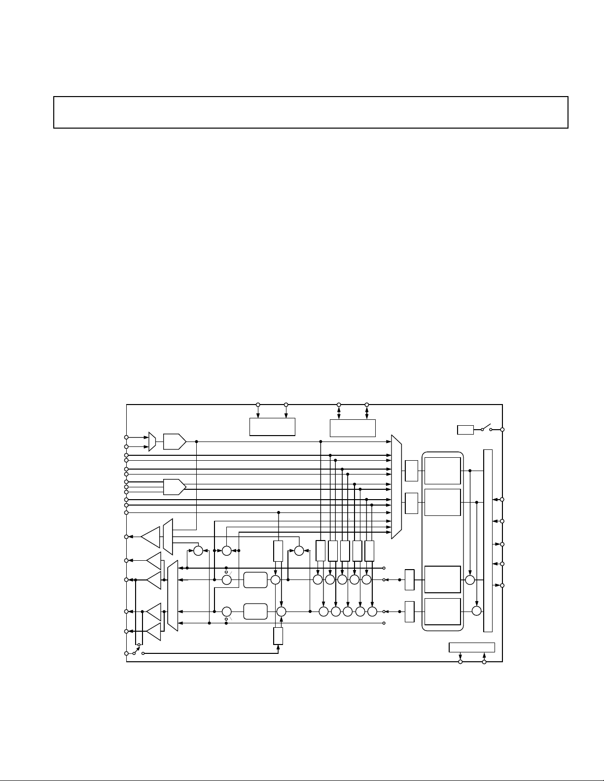
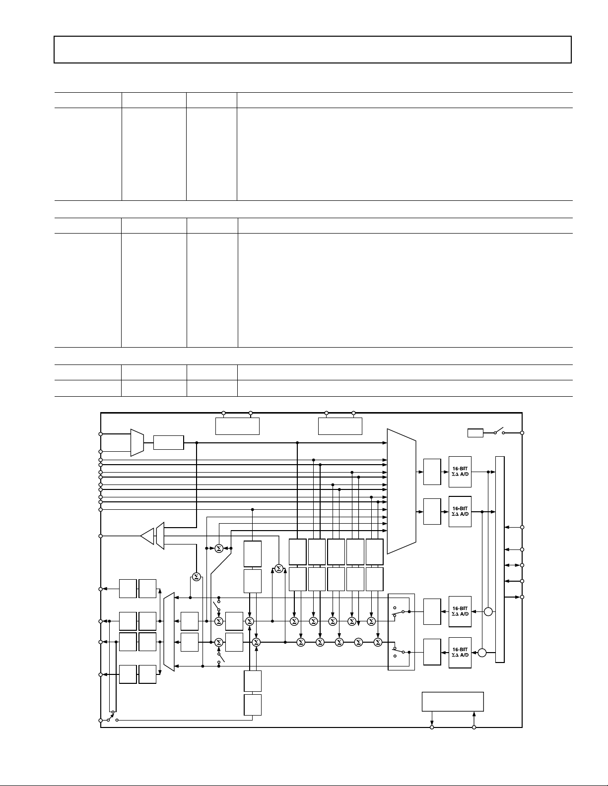
FUNCTIONAL BLOCK DIAGRAM
ID0 ID1
MIC1
MIC2
LINE
AUX
CD
VIDEO
PHONE_IN
MONO_OUT
HP_OUT_L
LINE_OUT_L
MMV
HV
MV
AD1885
0dB/
20dB
⌺
⌺
⌺
POP
CHIP SELECT
PHAT
STEREO
G
A
M
⌺
ENHANCED FEATURES
Full Duplex Variable Sample Rates from 7040 Hz to
48 kHz with 1 Hz Resolution
Jack Sense Pins Provide Automatic Output Switching
Software-Enabled V
Output for Microphones and
REFOUT
External Power Amp
Split Power Supplies (3.3 V Digital/5 V Analog)
Mobile Low-Power Mixer Mode
Extended 6-Bit Master Volume Control
Extended 6-Bit Headphone Volume Control
Digital Audio Mixer Mode
PHAT™ Stereo 3D Stereo Enhancement
JS0/EAPD JS1
JACK SENSES
AND EAPD CTRL
PGA
CONVERTER
SELECTOR
PGA
CONVERTER
G
G
G
⌺
A
M
⌺ ⌺
A
M
G
G
A
A
A
M
M
M
NC
⌺
⌺
⌺
⌺
G
A
M
GENERATORS
CONVERTER
16-BIT
⌺⌬ A/D
16-BIT
⌺⌬ A/D
SAMPLE
RATE
16-BIT
⌺⌬ D/A
V
REF
AC LINK
⌺
V
REFOUT
RESET
SYNC
BIT_CLK
SDATA_OUT
SDATA_IN
LINE_OUT_R
HP_OUT_R
PC_BEEP
MV
HV
⌺
POP
PHAT
STEREO
⌺
A
M
⌺ ⌺ ⌺ ⌺
G = GAIN
A = ATTENUATE
M = MUTE
MV = MASTER VOLUME
HV = HEADPHONE VOLUME
SoundPort is a registered trademark and PHAT is a trademark of Analog Devices, Inc.
REV. 0
Information furnished by Analog Devices is believed to be accurate and
reliable. However, no responsibility is assumed by Analog Devices for its
use, nor for any infringements of patents or other rights of third parties
which may result from its use. No license is granted by implication or
otherwise under any patent or patent rights of Analog Devices.
One Technology Way, P.O. Box 9106, Norwood, MA 02062-9106, U.S.A.
Tel: 781/329-4700 World Wide Web Site: http://www.analog.com
Fax: 781/326-8703 © Analog Devices, Inc., 2000
16-BIT
G
⌺
NC
A
M
⌺⌬ D/A
CONVERTER
OSCILLATOR
XTL_OUT
⌺
XTL_IN

AD1885–SPECIFICATIONS
STANDARD TEST CONDITIONS UNLESS OTHERWISE NOTED
Temperature 25 °C
Digital Supply (DV
Analog Supply (AV
Sample Rate (F
) 3.3 V
DD
) 5.0 V
DD
) 48 kHz
S
Input Signal 1008 Hz
Analog Output Passband 20 Hz to 20 kHz
ANALOG INPUT
Parameter Min Typ Max Unit
Input Voltage (RMS Values Assume Sine Wave Input)
LINE_IN, AUX, CD, VIDEO, PHONE_IN, PC_BEEP 1 V rms
MIC with 20 dB Gain (M20 = 1) 0.1 V rms
MIC with 0 dB Gain (M20 = 0) 1 V rms
Input Impedance* 20 kΩ
Input Capacitance* 5 7.5 pF
DAC Test Conditions
Calibrated
–3 dB Attenuation Relative to Full Scale
Input 0 dB
10 kΩ Output Load (LINE_OUT)
32 Ω Output Load (HP_OUT)
ADC Test Conditions
Calibrated
0 dB Gain
Input –3.0 dB Relative to Full Scale
2.83 V
0.283 V p-p
2.83 V p-p
p-p
MASTER VOLUME
Parameter Min Typ Max Unit
Step Size (0 dB to –94.5 dB); LINE_OUT_L, LINE_OUT_R 1.5 dB
Output Attenuation Range Span* –94.5 dB
Step Size (0 dB to –46.5 dB); MONO_OUT 1.5 dB
Output Attenuation Range Span* –46.5 dB
Step Size (+6 dB to –88.5 dB); HP_OUT_R, HP_OUT_L 1.5 dB
Output Attenuation Range Span* –94.5 dB
Mute Attenuation of 0 dB Fundamental* 80 dB
PROGRAMMABLE GAIN AMPLIFIER—ADC
Parameter Min Typ Max Unit
Step Size (0 dB to 22.5 dB) 1.5 dB
PGA Gain Range Span 22.5 dB
ANALOG MIXER—INPUT GAIN/AMPLIFIERS/ATTENUATORS
Parameter Min Typ Max Unit
Signal-to-Noise Ratio (SNR)
CD to LINE_OUT 90 dB
Other to LINE_OUT 90 dB
Step Size (+12 dB to –34.5 dB): (All Steps Tested)
MIC, LINE_IN, AUX, CD, VIDEO, PHONE_IN, DAC 1.5 dB
Input Gain/Attenuation Range: MIC, LINE, AUX, CD, VIDEO, PHONE_IN, DAC –46.5 dB
Step Size (0 dB to –45 dB): (All Steps Tested) PC_BEEP 3.0 dB
Input Gain/Attenuation Range: PC_BEEP –45 dB
* Guaranteed, not tested.
–2–
REV. 0

AD1885
DIGITAL DECIMATION AND INTERPOLATION FILTERS*
Parameter Min Typ Max Unit
Passband 0 0.4 × F
Passband Ripple ± 0.09 dB
Transition Band 0.4 × F
Stopband 0.6 × F
S
S
0.6 × FSHz
∞ Hz
Stopband Rejection –74 dB
Group Delay 12/F
Group Delay Variation Over Passband 0.0 µs
ANALOG-TO-DIGITAL CONVERTERS
Parameter Min Typ Max Unit
Resolution 16 Bits
Total Harmonic Distortion (THD –84 dB
Dynamic Range (–60 dB Input THD+N Referenced to Full Scale, A-Weighted) 84 87 dB
Signal-to-Intermodulation Distortion* (CCIF Method) 85 dB
ADC Crosstalk*
Line Inputs (Input L, Ground R, Read R; Input R, Ground L, Read L) –100 –90 dB
LINE_IN to Other –90 –85 dB
Gain Error (Full-Scale Span Relative to Nominal Input Voltage) ± 10 %
Interchannel Gain Mismatch (Difference of Gain Errors) ± 0.5 dB
ADC Offset Error ± 5mV
Hz
S
sec
S
DIGITAL-TO-ANALOG CONVERTERS
Parameter Min Typ Max Unit
Resolution 16 Bits
Total Harmonic Distortion (THD) LINE_OUT –85 dB
Total Harmonic Distortion (THD) HP_OUT (With 10 kΩ Load) –75 dB
Dynamic Range LINE_OUT (–60 dB Input THD+N Referenced to Full Scale,
A-Weighted) 85 90 dB
Signal-to-Intermodulation Distortion* (CCIF Method) –100 dB
Gain Error (Full-Scale Span Relative to Nominal Input Voltage) ± 10 %
Interchannel Gain Mismatch (Difference of Gain Errors) ± 0.7 dB
DAC Crosstalk* (Input L, Zero R, Measure R_OUT; Input R, Zero L,
Measure L_OUT) –80 dB
Total Audible Out-of-Band Energy (Measured from 0.6 × FS to 20 kHz)* –40 dB
ANALOG OUTPUT
Parameter Min Typ Max Unit
Full-Scale Output Voltage; LINE_OUT 1 V rms
2.83 V p-p
Output Impedance* 800 Ω
External Load Impedance* 10 kΩ
Output Capacitance* 15 pF
External Load Capacitance 100 pF
Full-Scale Output Voltage; HP_OUT (0 dB Gain) 1 V rms
Output Capacitance* 100 pF
External Load Capacitance 32 Ω
V
REF
V
REFOUT
V
REFOUT
Current Drive 5mA
2.05 2.25 2.45 V
2.25 V
Mute Click (Muted Output Minus Unmuted Midscale DAC Output) ± 5mV
*Guaranteed, not tested.
REV. 0
–3–

AD1885–SPECIFICATIONS
STATIC DIGITAL SPECIFICATIONS*
Parameter Min Typ Max Unit
High-Level Input Voltage (V
Low-Level Input Voltage (V
High-Level Output Voltage (V
Low-Level Output Voltage (V
): Digital Inputs 0.65 × DV
IH
) 0.35 × DVDDV
IL
), IOH = 2 mA 0.9 × DV
OH
), IOL = 2 mA 0.1 × DV
OL
DD
DD
Input Leakage Current –10 10 µA
Output Leakage Current –10 10 µA
POWER SUPPLY
Parameter Min Typ Max Unit
Power Supply Range—Analog (AV
Power Supply Range—Digital (DV
) 4.75 5.25 V
DD
) 3.15 3.45 V
DD
Power Dissipation—5 V/3.3 V 355 mW
Analog Supply Current—5 V (AV
Digital Supply Current—3.3 V (DV
)50mA
DD
)21mA
DD
Power Supply Rejection (100 mV p-p Signal @ 1 kHz)* 40 dB
(At Both Analog and Digital Supply Pins, Both ADCs and DACs)
CLOCK SPECIFICATIONS
Parameter Min Typ Max Unit
Input Clock Frequency 24.576 MHz
Recommended Clock Duty Cycle 40 50 60 %
DD
V
V
V
POWER-DOWN MODE*
DVDD (3.3 V) AVDD (5 V)
Parameter Set Bits Typ Typ Unit
ADC PR0 20 44 mA
DAC PR1 20 41 mA
ADC and DAC PR1, PR0 8 35 mA
ADC + DAC + Mixer (Analog CD On) LPMIX, PR1, PR0 8 26 mA
Mixer PR2 21 23 mA
ADC + Mixer PR2, PR0 19 18 mA
DAC + Mixer PR2, PR1 19 15 mA
ADC + DAC + Mixer PR2, PR1, PR0 8 10 mA
Analog CD Only (AC-Link On) LPMIX, PR5, PR1, PR0 7 22 mA
Analog CD Only (AC-Link Off) LPMIX, PR1, PR0, PR4, PR5 0 12 mA
Standby PR5, PR4, PR3, PR2, PR1, PR0 0 0.1 mA
Headphone Standby PR6 21 38 mA
NOTES
*Guaranteed, not tested.
Output jitter is directly dependent on crystal input jitter.
Specifications subject to change without notice.
–4–
REV. 0

AD1885
TIMING PARAMETERS (GUARANTEED OVER OPERATING TEMPERATURE RANGE)
Parameter Symbol Min Typ Max Unit
RESET Active Low Pulsewidth t
RESET Inactive to BIT_CLK Startup Delay t
SYNC Active High Pulsewidth t
SYNC Low Pulsewidth t
SYNC Inactive to BIT_CLK Startup Delay t
RST_LOW
RST2CLK
SYNC_HIGH
SYNC_LOW
SYNC2CLK
162.8 ns
162.8 ns
BIT_CLK Frequency 12.288 MHz
BIT_CLK Period t
CLK_PERIOD
BIT_CLK Output Jitter* 750 ps
BIT_CLK High Pulsewidth t
BIT_CLK Low Pulsewidth t
CLK_HIGH
CLK_LOW
32.56 42 48.84 ns
32.56 38 48.84 ns
SYNC Frequency 48.0 kHz
SYNC Period t
Setup to Falling Edge of BIT_CLK t
Hold from Falling Edge of BIT_CLK t
BIT_CLK Rise Time t
BIT_CLK Fall Time t
SYNC Rise Time t
SYNC Fall Time t
SDATA_IN Rise Time t
SDATA_IN Fall Time t
SDATA_OUT Rise Time t
SDATA_OUT Fall Time t
End of Slot 2 to BIT_CLK, SDATA_IN Low t
Setup to Trailing Edge of RESET (Applies to SYNC, SDATA_OUT) t
Rising Edge of RESET to HI-Z Delay t
SYNC_PERIOD
SETUP
HOLD
RISECLK
FALLCLK
RISESYNC
FALLSYNC
RISEDIN
FALLDIN
RISEDOUT
FALLDOUT
S2_PDOWN
SETUP2RST
OFF
5 2.5 ns
5ns
2410ns
2410ns
2410ns
2410ns
2410ns
2410ns
2410ns
2410ns
010ms
15 ns
Propagation Delay 15 ns
RESET Rise Time 50 ns
Output Valid Delay from Rising Edge of BIT_CLK to SDI Valid 15 ns
NOTES
*Output jitter is directly dependent on crystal input jitter.
Specifications subject to change without notice.
1.0 µs
1.3 µs
19.5 µs
81.4 ns
20.8 µs
25 ns
REV. 0
–5–
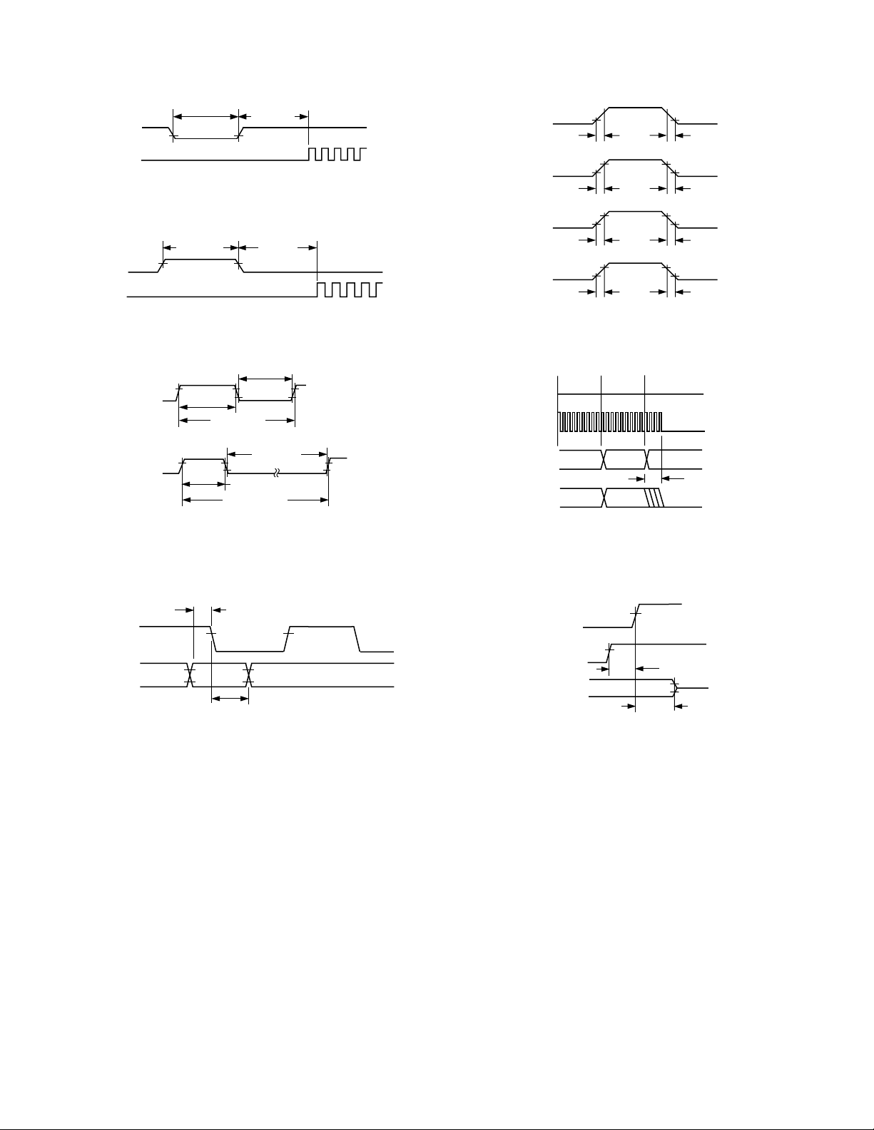
AD1885
RESET
BIT_CLK
SYNC
BIT_CLK
BIT_CLK
t
RST_LOW
t
RST2CLK
Figure 1. Cold Reset
t
SYNC_HIGH
t
RST2CLK
Figure 2. Warm Reset
t
CLK_LOW
t
CLK_HIGH
t
CLK_PERIOD
BIT_CLK
t
RISECLK
SYNC
t
RISESYNC
SDATA_IN
t
RISEDIN
SDATA_OUT
t
RISEDOUT
Figure 5. Signal Rise and Fall Time
SYNC
BIT_CLK
SLOT 1
SLOT 2
t
FALLCLK
t
FALLSYNC
t
FALLDIN
t
FALLDOUT
BIT_CLK
SYNC
SDATA_OUT
t
SYNC
SYNC_LOW
t
SYNC_HIGH
t
SYNC_PERIOD
Figure 3. Clock Timing
t
SETUP
t
HOLD
Figure 4. Data Setup and Hold
SDATA_OUT
SDATA_IN
WRITE
TO 0x26
NOTE: BIT_CLK NOT TO SCALE
DATA
PR4
DON’T
CARE
t
S2_PDOWN
Figure 6. AC-Link Low Power Mode Timing
RESET
SDATA_OUT
SDATA_IN, BIT_CLK
t
OFF
t
SETUP2RST
HI-Z
Figure 7. ATE Test Mode
–6–
REV. 0
AD1885
WARNING!
ESD SENSITIVE DEVICE
ABSOLUTE MAXIMUM RATINGS*
Parameter Min Max Unit
Power Supplies
Digital (AV
Analog (DV
) –0.3 +3.6 V
DD
) –0.3 +6.0 V
DD
Input Current (Except Supply Pins) ± 10 mA
Analog Input Voltage (Signal Pins) –0.3 AV
Digital Input Voltage (Signal Pins) –0.3 DV
+ 0.3 V
DD
+ 0.3 V
DD
Ambient Temperature (Operating) 0 70 °C
Storage Temperature –65 +150 °C
*Stresses greater than those listed under Absolute Maximum Ratings may cause
permanent damage to the device. This is a stress rating only; functional operation
of the device at these or any other conditions above those indicated in the
operational section of this specification is not implied. Exposure to absolu te maximum
rating conditions for extended periods may affect device reliability.
Model Range Description Option*
AD1885JST 0°C to 70°C 48-Lead LQFP ST-48
*ST = Thin Quad Flatpack.
ENVIRONMENTAL CONDITIONS
Ambient Temperature Rating
T
= T
T
P
θ
θ
θ
AMB
CASE
D
CA
JA
JC
CASE
= Case Temperature in °C
= Power Dissipation in W
= Thermal Resistance (Case-to-Ambient)
= Thermal Resistance (Junction-to-Ambient)
= Thermal Resistance (Junction-to-Case)
Package
ORDERING GUIDE
Temperature Package Package
– (PD × θCA)
JA
LQFP 76.2°C/W 17°C/W 59.2°C/W
CAUTION
ESD (electrostatic discharge) sensitive device. Electrostatic charges as high as 4000 V readily
accumulate on the human body and test equipment and can discharge without detection. Although
the AD1885 features proprietary ESD protection circuitry, permanent damage may occur on
devices subjected to high-energy electrostatic discharges. Therefore, proper ESD precautions are
recommended to avoid performance degradation or loss of functionality.
JC
CA
DV
DD1
XTL_IN
XTL_OUT
DV
SS1
SDATA_OUT
BIT_CLK
DV
SS2
SDATA_IN
DV
DD2
SYNC
RESET
PC_BEEP
NC = NO CONNECT
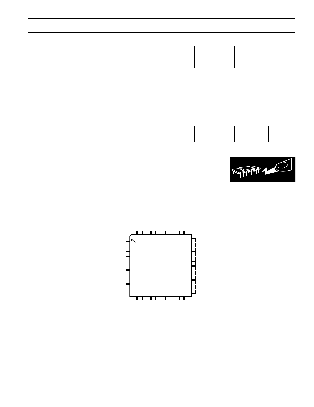
PIN CONFIGURATION
DD3AVSS3
NC
ID1
ID0
AD1885
TOP VIEW
(Not to Scale)
AUX_R
VIDEO_L
VIDEO_R
AV
19 20
CD_L
CD_GND_REF
JS0 (EAPD)
JS1
48
47 46 45 44 39 38 3743 42 41 40
1
PIN 1
IDENTIFIER
2
3
4
5
6
7
8
9
10
11
12
13 14 15 16 17 18
AUX_L
PHONE_IN
SS2
HP_OUT_L
AV
HP_OUT_R
21 22 23 24
MIC1
MIC2
CD_R
DD2
AV
36
35
34
33
32
31
30
29
28
27
26
25
LINE_IN_L
LINE_IN_R MONO_OUT
LINE_OUT_R
LINE_OUT_L
CX3D
RX3D
FILT_L
FILT_R
AFILT2
AFILT1
V
REFOUT
V
REF
AV
SS1
AV
DD1
–7–REV. 0
AD1885–SPECIFICATIONS
PIN FUNCTION DESCRIPTIONS
Digital I/O
Pin Name LQFP I/O Description
XTL_IN 2 I Crystal (or Clock) Input, 24.576 MHz.
XTL_OUT 3 O Crystal Output.
SDATA_OUT 5 I AC-Link Serial Data Output, AD1885 Input Stream.
BIT_ CLK 6 O/I AC-Link Bit Clock. 12.288 MHz Serial Data Clock. Daisy Chain Input Clock.
SDATA_IN 8 O AC-Link Serial Data Input. AD1885 Output Stream.
SYNC 10 I AC-Link Frame Sync.
RESET 11 I AC-Link Reset. AD1885 Master H/W Reset.
CHIP SELECTS
Pin Name LQFP Type Description
ID0 45 I Chip Select Input 0 (Active Low).
ID1 46 I Chip Select Input 1 (Active Low).
JACK SENSES/EAPD/GENERAL-PURPOSE DIGITAL OUTPUTS
These signals can sense the presence of audio jacks in the line-out or headphones outputs, and automatically mute the other audio
outputs. JS0 can also be programmed for EAPD control. Alternatively, both pins can be programmed as general-purpose digital outputs.
Pin Name LQFP Type Description
JS0 47 I/O JACK Sense Input 0 (Mutes Mono Output).
JS1 48 I/O JACK Sense Input 1 (Mutes Line_Out and Mono Outputs, or Line_Out Only).
Analog I/O
These signals connect the AD1885 component to analog sources and sinks, including microphones and speakers.
Pin Name LQFP I/O Description
PC_BEEP 12 I PC Beep. PC speaker beep passthrough.
PHONE_IN 13 I Phone Input. From telephony subsystem speakerphone or handset.
AUX_L 14 I Auxiliary Input Left Channel.
AUX_R 15 I Auxiliary Input Right Channel.
VIDEO_L 16 I Video Audio Left Channel.
VIDEO_R 17 I Video Audio Right Channel.
CD_L 18 I CD Audio Left Channel.
CD_GND_REF 19 I CD Audio Analog Ground Reference for Differential CD Input.
CD_ R 20 I CD Audio Right Channel.
MIC1 21 I Microphone 1. Desktop microphone input.
MIC2 22 I Microphone 2. Second microphone input.
LINE_IN_L 23 I Line In Left Channel.
LINE_IN_R 24 I Line In Right Channel.
LINE_OUT_L 35 O Line Out Left Channel.
LINE_OUT_R 36 O Line Out Right Channel.
MONO_OUT 37 O Monaural Output to Telephony Subsystem Speakerphone.
HP_OUT_L 39 O Headphones Out Left Channel.
HP_OUT_R 41 O Headphones Out Right Channel.
–8–
REV. 0
Filter/Reference
These signals are connected to resistors, capacitors, or specific voltages.
Pin Name LQFP I/O Description
V
REF
V
REFOUT
27 O Voltage Reference Filter.
28 O Voltage Reference Output 5 mA Drive (Intended for Mic Bias).
AFILT1 29 O Antialiasing Filter Capacitor—ADC Right Channel.
AFLIT2 30 O Antialiasing Filter Capacitor—ADC Left Channel.
FILT_R 31 O AC-Coupling Filter Capacitor—ADC Right Channel.
FILT_L 32 O AC-Coupling Filter Capacitor—ADC Left Channel.
RX3D 33 O 3D PHAT Stereo Enhancement—Resistor.
CX3D 34 I 3D PHAT Stereo Enhancement—Capacitor.
Power and Ground Signals
Pin Name LQFP Type Description
DV
DV
DV
DV
AV
AV
AV
AV
AV
AV
DD1
SS1
SS2
DD2
DD1
SS1
DD2
SS2
DD3
SS3
1 I Digital VDD 3.3 V
4 I Digital GND
7 I Digital GND
9 I Digital VDD 3.3 V
25 I Analog VDD 5.0 V
26 I Analog GND
38 I Analog VDD 5.0 V
40 I Analog GND
43 I Analog VDD 5.0 V
44 I Analog GND
No Connects
Pin Name LQFP Type Description
NC 42 No Connect
AD1885
MIC1
MIC2
LINE
AUX
VIDEO
PHONE_IN
MONO_OUT
HP_OUT_L
LINE_OUT_L
LINE_OUT_R
HP_OUT_R
PC_BEEP
GA
0x0E
MCV
0x0E
MCM
M
JS0/EAPD JS1
JACK SENSE
AND EAPD CTRL
GA
GA
0x10
0x12
LLV
LCV
RLV
RCV
M
M
0x10
0x12
LM
CM
G = GAIN
A = ATTENUATION
M = MUTE
S = SELECTOR
GA
0x16
LAV
RAV
0x16
AM
V
AC-LINK
REFOUT
RESET
SYNC
BIT_CLK
SDATA_OUT
SDATA_IN
V
LS/RS (0)
LS (4)
RS (4)
LS (3)
RS (3)
LS (1)
RS (1)
LS (2)
RS (2)
LS/RS (7)
LS (5)
LS/RS (6)
RS (5)
S 0x1A
GA
0x14
LVV
RVV
M
M
0x14
VM
A
3D 0x20
SWITCH
B
NC
NC
S
E
L
E
C
T
O
R
AD1885
XTL_OUT
GAM
0x1C
LIV
IM
GAM
0x1C
RIV
IM
GAM
0x18
LOV
OM
GAM
0x18
ROV
OM
OSCILLATORS
REF
⌺
⌺
XTL_IN
ID1ID0
0
0dB/20dB
MS
M20 0x0E
1
S 0ⴛ20
CD
MV
MIX
0x20
0x04
0x04
LHV
HPM
0x02
0x02
MM
0x02
MM
0x04
HPM
LMV
0x02
LMV
0x04
RHV
0x22
D
DP
A
0x22
M
DP
CHIP SELECT
POP
PHAT
0x20
PHAT
0x20
POP
STEREO MIX (L)
MONO MIX
STEREO MIX (R)
GA
0x0C
PHV
M
0x0C
PHM
M
0x0A
PCM
A
0x0A
PCV
Figure 8. Block Diagram Register Map
–9–REV. 0

AD1885
PRODUCT OVERVIEW
The AD1885 Codec meets the Audio Codec ’97 2.1 Extensions,
adding support for multiple Codecs and variable sample rates.
In addition, the AD1885 SoundPort Codec is designed to meet
all requirements of the Audio Codec ’97, Component Specification,
Revision 1.03, © 1996, Intel Corporation, found at www.Intel.com.
The AD1885 also includes other Codec enhanced features such
as communicating to three Codecs on the same link, integrated
headphone driver and built-in PHAT Stereo 3D enhancement.
The AD1885 is an analog front end for high-performance PC
audio, modem, or DSP applications. The AC’97 architecture
defines a 2-chip audio solution comprising a digital audio
controller, plus a high-quality analog component that includes
Digital-to-Analog Converters (DACs), Analog-to-Digital Converters (ADCs), mixer, and I/O.
The main architectural features of the AD1885 are the high
quality analog mixer section, two channels of Σ∆ ADC conversion, two channels of Σ∆ DAC conversion and Data Direct
Scrambling (D
FUNCTIONAL DESCRIPTION
2
S) rate generators.
This section overviews the functionality of the AD1885 and is
intended as a general introduction to the capabilities of the
device. Detailed reference information may be found in the
descriptions of the Indexed Control Registers.
Analog Inputs
The Codec contains a stereo pair of Σ∆ ADCs. Inputs to the
ADC may be selected from the following analog signals: telephony (PHONE_IN), mono microphone (MIC1 or MIC2),
stereo line (LINE_IN), auxiliary line input (AUX), stereo CD
ROM (CD), stereo audio from a video source (VIDEO) and
post-mixed stereo or mono line output (LINE_OUT).
Analog Mixing
PHONE_IN, MIC1 or MIC2, LINE_IN, AUX, CD, and VIDEO
can be mixed in the analog domain with the stereo output from the
DACs. Each channel of the stereo analog inputs may be independently gained or attenuated from +12 dB to –34.5 dB in 1.5 dB
steps. The summing path for the mono inputs (PHONE_IN, MIC1,
and MIC2 to LINE_OUT and HP_OUT) duplicates mono channel data on both the left and right LINE_OUT and HP_OUT.
Additionally, the PC attention signal (PC_BEEP) may be mixed
with the line output and headphone. A switch allows the output
of the DACs to bypass the PHAT Stereo 3D enhancement.
Digital Audio Mode
The AD1885 is designed with a Digital Audio Mode (DAM)
that allows mixing of all analog inputs, independent of the DAC
output signal path. Mixed analog input signals may be sent to
the ADCs for processing by the DC ’97 controller or the host,
and may be used during simultaneous capture and playback at
different sample rates.
Analog-to-Digital Signal Path
The selector sends left and right channel information to the
programmable gain amplifier (PGA). The PGA following the
selector allows independent gain control for each channel entering the ADC from 0 dB to +22.5 dB in 1.5 dB steps. Each
channel of the ADC is independent, and can process left and
right channel data at different sample rates.
Sample Rates and D2S
The AD1885 default mode sets the Codec to operate at 48 kHz
sample rates. The converter pairs may process left and right
channel data at different sample rates. The AD1885 sample rate
generator allows the Codec to instantaneously change and process
sample rates from 7040 Hz to 48 kHz with a resolution of 1 Hz.
The in-band integrated noise and distortion artifacts introduced
by rate conversions are below –90 dB. The AD1885 uses a 4-bit
Σ∆ structure and D
boards and in PC enclosures, and to suppress idle tones below
the device’s quantization noise floor. The D
2
S to enhance noise immunity on mother-
2
S process pushes
noise and distortion artifacts caused by errors in the multibit
DAC to frequencies beyond the auditory response of the human
ear and then filters them.
Digital-to-Analog Signal Path
The analog output of the DAC may be gained or attenuated
from +12 dB to –34.5 dB in 1.5 dB steps, and summed with any
of the analog input signals. The summed analog signal enters
the Master Volume stage where each channel of the mixer output may be attenuated from 0 dB to –94.5 dB in 1.5 dB steps
or muted.
Analog Outputs
The AD1885 offers a line output controlled by the Master Volume
control and an integrated headphone driver with independent
control.
Host-Based Echo Cancellation Support
The AD1885 supports time correlated I/O data format by presenting mic data on the left channel of the ADC and the mono
summation of left and right output on the right channel. The
ADC is splittable; left and right ADC data can be sampled at
different rates.
Telephony Modem Support
The AD1885 contains a V.34-capable analog front end for supporting host-based and data pump modems. The modem DAC
typical dynamic range is 90 dB over a 4.2 kHz analog output
passband where F
= 12.8 kHz. The left channel of the ADC
S
and DAC may be used to convert modem data at the same
sample rate in the range between 7040 Hz and 48 kHz. All programmed sample rates have a resolution of 1 Hz. The AD1885
supports irrational V.34 sample rates with 8/7 and 10/7 selectable multiplier coefficients.
Power Management Modes
The AD1885 is designed to meet notebook and ACPI power
consumption requirements through flexible power management
control of all internal resources. The following subsections may
be independently controlled:
ADCs and Input Mux Power-Down
DACs Power-Down
Analog Mixer Power-Down
Digital Interface Power-Down
Internal Clocks Disabled
ADC and DAC Power-Down
VREF Standby Mode
Low-Power Mixer Mode—CD Mixer Alive Only Mode
Mixer Bypass Mode (Digital Audio)
Headphone
–10–
REV. 0

AD1885
Indexed Control Registers
Reg
Num Name D15 D14 D13 D12 D11 D10 D9 D8 D7 D6 D5 D4 D3 D2 D1 D0 Default
00h Reset X SE4 SE3 SE2 SE1 SE0 ID9 ID8 ID7 ID6 ID5 ID4 ID3 ID2 ID1 ID0 0410h
02h Master Volume MM X LMV5 LMV4 LMV3 LMV2 LMV1 LMV0 X X RMV5 RMV4 RMV3 RMV2 RMV1 RMV0 8000h
04h Headphones Volume HPM X LHV5 LHV4 LHV3 LHV2 LHV1 LHV0 X X RHV5 RHV4 RHV3 RHV2 RHV1 RHV0 8000h
06h Master Volume Mono MMM X X X X X X X X X X MMV MMV MMV MMV MMV 8000h
43210
08h Reserved X X X X X X X X X X X X X X X X X
0Ah PC Beep Volume PCM X X X X X X X X X X PCV3 PCV2 PCV1 PCV0 X 8000h
0Ch Phone In Volume PHM X X X X X X X X X X PHV4 PHV3 PHV2 PHV1 PHV0 8008h
0Eh MIC Volume MCM X X X X X X X X M20 X MCV4 MCV3 MCV2 MCV1 MCV0 8008h
10h Line In Volume LM X X LLV4 LLV3 LLV2 LLV1 LLV0 X X X RLV4 RLV3 RLV2 RLV1 RLV0 8808h
12h CD Volume CVM X X LCV4 LCV3 LCV2 LCV1 LCV0 X X X RCV4 RCV3 RCV2 RCV1 RCV0 8808h
14h Video Volume VM X X LVV4 LVV3 LVV2 LVV1 LVV0 X X X RVV4 RVV3 RVV2 RVV1 RVV0 8808h
16h Aux Volume AM X X LAV4 LAV3 LAV2 LAV1 LAV0 X X X RAV4 RAV3 RAV2 RAV1 RAV0 8808h
18h PCM Out Volume OM X X LOV4 LOV3 LOV2 LOV1 LOV0 X X X ROV4 ROV3 ROV2 ROV1 ROV0 8808h
1Ah Record Select X X X X X LS2 LS1 LS0 X X X X X RS2 RS1 RS0 0000h
1Ch Record Gain IM X X X LIM3 LIM2 LIM1 LIM0 X X X X RIM3 RIM2 RIM1 RIM0 8000h
1Eh Reserved X X X X X X X X X X X X X X X X X
20h General Purpose POP X 3D X X X MIX MS LPBK X X X X X X X 0000h
22h 3D Control X X X X X X X X X X X X DP3 DP2 DP1 DP0 0000h
26h Power-Down Cntrl/Stat X X PR5 PR4 PR3 PR2 PR1 PR0 X X X X REF ANL DAC ADC 000Xh
28h Extended Audio ID ID1 ID0 X X X X X X X X X X X X X VRA 0001h
2Ah Extended Audio Stat/Ctrl X X X X X X X X X X X X X X X VRA 0000h
2Ch/ PCM DAC Rate (SR1) SR15 SR14 SR13 SR12 SR11 SR10 SR9 SR8 SR7 SR6 SR5 SR4 SR3 SR2 SR1 SR0 BB80h
(7Ah)*
32h/ PCM ADC Rate (SR0) SR15 SR14 SR13 SR12 SR11 SR10 SR9 SR8 SR7 SR6 SR5 SR4 SR3 SR2 SR1 SR0 BB80h
(78h)*
34h Reserved X X X X X X X X X X X X X X X X X
.. .. .. .. .. .. .. .. .. .. .. .. .. .. .. .. .. .. ..
72h Jack Sense/Audio JS1_OUT JS0_ JS1 JS0 JS1_ JS0 JS1 JS0 JS1 JS0_ JS1 JS0 AUD JS1 JS0 JS 0000h
Interrupt/Status FUNCT OUT PUDIS PUDIS OE OE DIS DIS CLR CLR MODE MODE INT INT
74h Serial Configuration SLOT REG REG REG X X DHWR X X X X X X X X 7000h
16 M2 M1 M0
76h Miscellaneous Control DAC LPMI X DAM DMS DLSR X ALSR MOD SRX1 SRX8 X X DRSR X ARSR 0404h
Bits Z X EN 0D7 D7
7Ch Vendor ID1 F7 F6 F5 F4 F3 F2 F1 F0 S7 S6 S5 S4 S3 S2 S1 S0 4144h
7Eh Vendor ID2 T7 T6 T5 T4 T3 T2 T1 T0 REV7 REV6 REV5 REV4 REV3 REV2 REV1 REV0 5360h
NOTES
All registers not shown and bits containing an X are assumed to be reserved.
Odd register addresses are aliased to the next lower even address.
Reserved registers should not be written.
Zeros should be written to reserved bits.
*Indicates Aliased register for AD1819B backward compatibility.
–11–REV. 0

AD1885
Reset (Index 00h)
geRgeR
geRgeR
geR
muNmuN
muNmuN
muN
h00h00
h00h00teseRteseR
h00
Note: Writing any value to this register performs a register reset, which causes all registers to revert to their default values (except
74h, which forces the serial configuration). Reading this register returns the ID code of the part and a code for the type of 3D Stereo
Enhancement.
ID[9:0] Identify Capability. The ID decodes the capabilities of AD1885 based on the following:
SE[4:0] Stereo Enhancement. The 3D stereo enhancement identifies the Analog Devices 3D stereo enhancement.
Master Volume Registers (Index 02h)
emaNemaN
emaNemaN51D51D
emaN
teseRteseRXXXXX4ES4ES
teseR
51D51D41D41D
51D
41D41D31D31D
31D31D21D21D
21D21D11D11D
11D11D01D01D
41D
4ES4ES3ES3ES
4ES
31D
3ES3ES2ES2ES
3ES
21D
2ES2ES1ES1ES
2ES
01D01D9D9D9D9D9D8D8D8D8D8D7D7D7D7D7D6D6D6D6D6D5D5D5D5D5D4D4D4D4D4D3D3D3D3D3D2D2D2D2D2D1D1D1D1D1D0D0D0D0D0DtluafeDtluafeD
11D
01D
1ES1ES0ES0ES
0ES0ES9DI9DI
9DI9DI8DI8DI
8DI8DI7DI7DI
7DI7DI6DI6DI
6DI6DI5DI5DI
1ES
0ES
9DI
8DI
7DI
5DI5DI4DI4DI
6DI
5DI
Bit = 1 Function AD1885
ID0 Dedicated MIC PCM In Channel 0
ID1 Modem Line Codec Support 0
ID2 Bass and Treble Control 0
ID3 Simulated Stereo (Mono to Stereo) 0
ID4 Headphone Out Support 1
ID5 Loudness (Bass Boost) Support 0
ID6 18-Bit DAC Resolution 0
ID7 20-Bit DAC Resolution 0
ID8 18-Bit ADC Resolution 0
ID9 20-Bit ADC Resolution 0
4DI4DI3DI3DI
4DI
3DI3DI2DI2DI
3DI
2DI2DI1DI1DI
2DI
1DI1DI0DI0DI
1DI
0DI0DIh0140h0140
0DI
tluafeDtluafeD
tluafeD
h0140h0140
h0140
geRgeR
geRgeR
geR
muNmuN
muNmuN
muN
h20h20
h20h20
h20
emaNemaN
emaNemaN51D51D
emaN
retsaMretsaM
retsaMretsaM
retsaM
emuloVemuloV
emuloVemuloV
emuloV
51D51D41D41D
41D41D31D31D
51D
41D
MMMMMMMMMMXXXXX5VML5VML
31D31D21D21D
31D
5VML5VML4VML4VML
5VML
21D21D11D11D
21D
4VML4VML3VML3VML
4VML
11D11D01D01D
01D01D9D9D9D9D9D8D8D8D8D8D7D7D7D7D7D6D6D6D6D6D5D5D5D5D5D4D4D4D4D4D3D3D3D3D3D2D2D2D2D2D1D1D1D1D1D0D0D0D0D0DtluafeDtluafeD
11D
01D
3VML3VML2VML2VML
2VML2VML1VML1VML
1VML1VML0VML0VML
3VML
2VML
0VML0VMLXXXXXXXXXX5VMR5VMR
1VML
0VML
5VMR5VMR4VMR4VMR
5VMR
4VMR4VMR3VMR3VMR
4VMR
3VMR3VMR2VMR2VMR
3VMR
2VMR2VMR1VMR1VMR
2VMR
1VMR1VMR0VMR0VMR
1VMR
0VMR0VMRh0008h0008
0VMR
tluafeDtluafeD
tluafeD
h0008h0008
h0008
RMV[5:0] Right Master Volume Control. The least significant bit represents 1.5 dB. This register controls the output from
0 dB to a maximum attenuation of –94.5 dB.
LMV[5:0] Left Master Volume Control. The least significant bit represents 1.5 dB. This register controls the output from 0 dB to
a maximum attenuation of –94.5 dB.
MM Master Volume Mute. When this bit is set to “1,” the channel is muted.
MM xMV5 . . . xMV0 Function
0 00 0000 0 dB Attenuation
0 01 1111 –46.5 dB Attenuation
0 11 1111 –94.5 dB Attenuation
1 xx xxxx –∞ dB Attenuation
–12–
REV. 0

AD1885
Headphones Volume Registers (Index 04h)
geRgeR
geRgeR
geR
muNmuN
muNmuN
muN
h40h40
h40h40emuloVsenohpdaeHemuloVsenohpdaeH
h40
RHV[5:0] Right Headphone Volume Control. The least significant bit represents 1.5 dB. This register controls the out-
LHV[5:0] Left Headphone Volume Control. The least significant bit represents 1.5 dB. This register controls the output
HPM Headphone Volume Mute. When this bit is set to “1,” the channel is muted.
Master Volume Mono (Index 06h)
geRgeR
geRgeR
geR
muNmuN
muNmuN
muN
emaNemaN
emaNemaN51D51D
emaN
emuloVsenohpdaeHemuloVsenohpdaeHMPHMPH
emuloVsenohpdaeH
51D51D41D41D
41D41D31D31D
51D
41D
MPHMPHXXXXX5VHL5VHL
MPH
31D31D21D21D
31D
5VHL5VHL4VHL4VHL
5VHL
21D21D11D11D
21D
4VHL4VHL3VHL3VHL
4VHL
11D11D01D01D
01D01D9D9D9D9D9D8D8D8D8D8D7D7D7D7D7D6D6D6D6D6D5D5D5D5D5D4D4D4D4D4D3D3D3D3D3D2D2D2D2D2D1D1D1D1D1D0D0D0D0D0DtluafeDtluafeD
11D
01D
3VHL3VHL2VHL2VHL
2VHL2VHL1VHL1VHL
3VHL
2VHL
put from +6 dB to a maximum attenuation of –88.5 dB.
from +6 dB to a maximum attenuation of –88.5 dB.
HPM xHV5 . . . xHV0 Function
0 00 0000 6 dB Gain
0 01 1111 –40.5 dB Attenuation
0 11 1111 –88.5 dB Attenuation
1 xx xxxx –∞ dB Attenuation
emaNemaN
emaNemaN51D51D
emaN
51D51D41D41D
51D
41D41D31D31D
41D
31D31D21D21D
31D
21D21D11D11D
21D
11D11D01D01D
01D01D9D9D9D9D9D8D8D8D8D8D7D7D7D7D7D6D6D6D6D6D5D5D5D5D5D4D4D4D4D4D3D3D3D3D3D2D2D2D2D2D1D1D1D1D1D0D0D0D0D0DtluafeDtluafeD
11D
01D
1VHL1VHL0VHL0VHL
1VHL
0VHL0VHLXXXXXXXXXX5VHR5VHR
0VHL
5VHR5VHR4VHR4VHR
5VHR
4VHR4VHR3VHR3VHR
4VHR
3VHR3VHR2VHR2VHR
3VHR
2VHR2VHR1VHR1VHR
2VHR
1VHR1VHR0VHR0VHR
1VHR
0VHR0VHRh0008h0008
0VHR
tluafeDtluafeD
tluafeD
h0008h0008
h0008
tluafeDtluafeD
tluafeD
emuloVretsaMemuloVretsaM
emuloVretsaMemuloVretsaM
h60h60
h60h60
h60
onoMonoM
onoMonoM
onoM
emuloVretsaM
MMMMMM
MMMMMMXXXXXXXXXXXXXXXXXXXXXXXXXXXXXXXXXXXXXXXXXXXXXXXXXX4VMM4VMM
MMM
4VMM4VMM3VMM3VMM
4VMM
3VMM3VMM2VMM2VMM
3VMM
2VMM2VMM1VMM1VMM
2VMM
1VMM1VMM0VMM0VMM
1VMM
0VMM0VMMh0008h0008
0VMM
h0008h0008
h0008
MMV[4:0] Mono Master Volume Control. The least significant bit represents 1.5 dB. This register controls the output from
0 dB to a maximum attenuation of 46.5 dB.
MMM Mono Master Volume Mute. When this bit is set to “1,” the channel is muted.
PC Beep Register (Index 0Ah)
geRgeR
geRgeR
geR
muNmuN
muNmuN
muN
hA0hA0
hA0hA0emuloVPEEB_CPemuloVPEEB_CP
hA0
emaNemaN
emaNemaN51D51D
emaN
emuloVPEEB_CPemuloVPEEB_CPMCPMCP
emuloVPEEB_CP
51D51D41D41D
41D41D31D31D
31D31D21D21D
21D21D11D11D
11D11D01D01D
51D
41D
31D
21D
MCPMCPXXXXXXXXXXXXXXXXXXXXXXXXXXXXXXXXXXXXXXXXXXXXXXXXXX3VCP3VCP
MCP
01D01D9D9D9D9D9D8D8D8D8D8D7D7D7D7D7D6D6D6D6D6D5D5D5D5D5D4D4D4D4D4D3D3D3D3D3D2D2D2D2D2D1D1D1D1D1D0D0D0D0D0DtluafeDtluafeD
11D
01D
3VCP3VCP2VCP2VCP
3VCP
2VCP2VCP1VCP1VCP
2VCP
1VCP1VCP0VCP0VCP
1VCP
0VCP0VCPXXXXXh0008h0008
0VCP
tluafeDtluafeD
tluafeD
h0008h0008
h0008
PCV[3:0] PC Beep Volume Control. The least significant bit represents 3 dB attenuation. This register controls the output
from 0 dB to a maximum attenuation of –45 dB. The PC Beep is routed to Left and Right Line outputs even when
AD1885 is in a RESET state. This is so that Power-On Self-Test (POST) codes can be heard by the user in case
of a hardware problem with the PC.
PCM PC Beep Mute. When this bit is set to “1,” the channel is muted.
PCM PCV3 . . . PCV0 Function
0 0000 0 dB Attenuation
0 1111 –45 dB Attenuation
1 xxxx ∞ dB Attenuation
–13–REV. 0

AD1885
Phone Volume (Index 0Ch)
geRgeR
geRgeR
geR
muNmuN
muNmuN
muN
hC0hC0
hC0hC0emuloVenohPemuloVenohP
hC0
PHV[4:0] Phone Volume. Allows setting the Phone Volume Attenuator in 32 steps. The LSB represents 1.5 dB, and the
PHM Phone Mute. When this bit is set to “1,” the channel is muted.
MIC Volume (Index 0Eh)
geRgeR
geRgeR
geR
muNmuN
muNmuN
muN
hE0hE0
hE0hE0
hE0
MCV[4:0] MIC Volume Gain. Allows setting the MIC Volume attenuator in 32 steps. The LSB represents 1.5 dB, and the
M20 Microphone 20 dB Gain Block
MCM MIC Mute. When this bit is set to “1,” the channel is muted.
Line In Volume (Index 10h)
emaNemaN
emaNemaN51D51D
emaN
range is +12 dB to –34.5 dB. The default value is 0 dB, mute enabled.
emaNemaN
emaNemaN51D51D
emaN
CIMCIM
CIMCIM
CIM
emuloVemuloV
emuloVemuloV
emuloV
range is +12 dB to –34.5 dB. The default value is 0 dB, mute enabled.
51D51D41D41D
41D41D31D31D
31D31D21D21D
21D21D11D11D
11D11D01D01D
51D
41D
31D
21D
emuloVenohPemuloVenohPMHPMHP
MHPMHPXXXXXXXXXXXXXXXXXXXXXXXXXXXXXXXXXXXXXXXXXXXXXXXXXX4VHP4VHP
emuloVenohP
MHP
51D51D41D41D
41D41D31D31D
31D31D21D21D
21D21D11D11D
51D
41D
31D
MCMMCM
MCMMCMXXXXXXXXXXXXXXXXXXXXXXXXXXXXXXXXXXXXXXXX02M02M
MCM
11D11D01D01D
21D
11D
01D01D9D9D9D9D9D8D8D8D8D8D7D7D7D7D7D6D6D6D6D6D5D5D5D5D5D4D4D4D4D4D3D3D3D3D3D2D2D2D2D2D1D1D1D1D1D0D0D0D0D0DtluafeDtluafeD
11D
01D
01D01D9D9D9D9D9D8D8D8D8D8D7D7D7D7D7D6D6D6D6D6D5D5D5D5D5D4D4D4D4D4D3D3D3D3D3D2D2D2D2D2D1D1D1D1D1D0D0D0D0D0DtluafeDtluafeD
01D
0 = Disabled; Gain = 0 dB
1 = Enabled; Gain = 20 dB.
02M02MXXXXX4VCM4VCM
02M
4VCM4VCM3VCM3VCM
4VCM
4VHP4VHP3VHP3VHP
4VHP
3VHP3VHP2VHP2VHP
3VHP
3VCM3VCM2VCM2VCM
3VCM
2VHP2VHP1VHP1VHP
2VHP
2VCM2VCM1VCM1VCM
2VCM
1VHP1VHP0VHP0VHP
1VHP
1VCM1VCM0VCM0VCM
1VCM
0VHP0VHPh8008h8008
0VHP
0VCM0VCMh8008h8008
0VCM
tluafeDtluafeD
tluafeD
h8008h8008
h8008
tluafeDtluafeD
tluafeD
h8008h8008
h8008
geRgeR
geRgeR
geR
muNmuN
muNmuN
muN
h01h01
h01h01emuloVnIeniLemuloVnIeniL
h01
emaNemaN
emaNemaN51D51D
emaN
emuloVnIeniLemuloVnIeniLMLMLMLMLMLXXXXXXXXXX4VLL4VLL
emuloVnIeniL
51D51D41D41D
51D
41D41D31D31D
41D
31D31D21D21D
31D
21D21D11D11D
21D
4VLL4VLL3VLL3VLL
4VLL
11D11D01D01D
01D01D9D9D9D9D9D8D8D8D8D8D7D7D7D7D7D6D6D6D6D6D5D5D5D5D5D4D4D4D4D4D3D3D3D3D3D2D2D2D2D2D1D1D1D1D1D0D0D0D0D0DtluafeDtluafeD
11D
01D
3VLL3VLL2VLL2VLL
2VLL2VLL1VLL1VLL
1VLL1VLL0VLL0VLL
3VLL
2VLL
0VLL0VLLXXXXXXXXXXXXXXX4VLR4VLR
1VLL
0VLL
4VLR4VLR3VLR3VLR
4VLR
3VLR3VLR2VLR2VLR
3VLR
2VLR2VLR1VLR1VLR
2VLR
1VLR1VLR0VLR0VLR
1VLR
0VLR0VLRh8088h8088
0VLR
tluafeDtluafeD
tluafeD
h8088h8088
h8088
RLV[4:0] Right Line In Volume. Allows setting the Line In right channel attenuator in 32 steps. The LSB represents 1.5 dB,
and the range is +12 dB to –34.5 dB. The default value is 0 dB, mute enabled.
LLV[4:0] Line In Volume Left. Allows setting the Line In left channel attenuator in 32 steps. The LSB represents 1.5 dB, and
the range is +12 dB to –34.5 dB. The default value is 0 dB, mute enabled.
LM Line In Mute. When this bit is set to “1,” the channel is muted.
CD Volume (Index 12h)
geRgeR
geRgeR
geR
muNmuN
muNmuN
muN
h21h21
h21h21emuloVDCemuloVDC
h21
emaNemaN
emaNemaN51D51D
emaN
emuloVDCemuloVDCMVCMVC
emuloVDC
51D51D41D41D
41D41D31D31D
51D
MVCMVCXXXXXXXXXX4VCL4VCL
MVC
31D31D21D21D
41D
31D
21D21D11D11D
21D
4VCL4VCL3VCL3VCL
4VCL
11D11D01D01D
01D01D9D9D9D9D9D8D8D8D8D8D7D7D7D7D7D6D6D6D6D6D5D5D5D5D5D4D4D4D4D4D3D3D3D3D3D2D2D2D2D2D1D1D1D1D1D0D0D0D0D0DtluafeDtluafeD
11D
01D
3VCL3VCL2VCL2VCL
2VCL2VCL1VCL1VCL
1VCL1VCL0VCL0VCL
3VCL
2VCL
0VCL0VCLXXXXXXXXXXXXXXX4VCR4VCR
1VCL
0VCL
4VCR4VCR3VCR3VCR
4VCR
3VCR3VCR2VCR2VCR
3VCR
2VCR2VCR1VCR1VCR
2VCR
1VCR1VCR0VCR0VCR
1VCR
0VCR0VCRh8088h8088
0VCR
tluafeDtluafeD
tluafeD
h8088h8088
h8088
RCV[4:0] Right CD Volume. Allows setting the CD right channel attenuator in 32 steps. The LSB represents 1.5 dB, and
the range is +12 dB to –34.5 dB. The default value is 0 dB, mute enabled.
LCV[4:0] Left CD Volume. Allows setting the CD left channel attenuator in 32 steps. The LSB represents 1.5 dB, and the
range is +12 dB to –34.5 dB. The default value is 0 dB, mute enabled.
CVM CD Volume Mute. When this bit is set to “1,” the channel is muted.
–14–
REV. 0

AD1885
Video Volume (Index 14h)
geRgeR
geRgeR
geR
muNmuN
muNmuN
muN
h41h41
h41h41emuloVoediVemuloVoediV
h41
RVV[4:0] Right Video Volume. Allows setting the Video right channel attenuator in 32 steps. The LSB represents 1.5 dB,
LVV[4:0] Left Video Volume. Allows setting the Video left channel attenuator in 32 steps. The LSB represents 1.5 dB, and
VM Video Mute. When this bit is set to “1,” the channel is muted.
AUX Volume (Index 16h)
geRgeR
geRgeR
geR
muNmuN
muNmuN
muN
h61h61
h61h61emuloVxuAemuloVxuA
h61
RAV[4:0] Right Aux Volume. Allows setting the Aux right channel attenuator in 32 steps. The LSB represents 1.5 dB, and
LAV[4:0] Left Aux Volume. Allows setting the Aux left channel attenuator in 32 steps. The LSB represents 1.5 dB, and the
AM Aux Mute. When this bit is set to “1,” the channel is muted.
PCM Out Volume (Index 18h)
emaNemaN
emaNemaN51D51D
emaN
51D51D41D41D
41D41D31D31D
51D
emuloVoediVemuloVoediVMVMVMVMVMVXXXXXXXXXX4VVL4VVL
emuloVoediV
31D31D21D21D
41D
31D
21D21D11D11D
21D
4VVL4VVL3VVL3VVL
4VVL
11D11D01D01D
01D01D9D9D9D9D9D8D8D8D8D8D7D7D7D7D7D6D6D6D6D6D5D5D5D5D5D4D4D4D4D4D3D3D3D3D3D2D2D2D2D2D1D1D1D1D1D0D0D0D0D0DtluafeDtluafeD
11D
01D
3VVL3VVL2VVL2VVL
2VVL2VVL1VVL1VVL
1VVL1VVL0VVL0VVL
3VVL
2VVL
0VVL0VVLXXXXXXXXXXXXXXX4VVR4VVR
1VVL
0VVL
and the range is +12 dB to –34.5 dB. The default value is 0 dB, mute enabled.
the range is +12 dB to –34.5 dB. The default value is 0 dB, mute enabled.
emaNemaN
emaNemaN51D51D
emaN
51D51D41D41D
41D41D31D31D
51D
emuloVxuAemuloVxuAMAMAMAMAMAXXXXXXXXXX4VAL4VAL
emuloVxuA
31D31D21D21D
41D
31D
21D21D11D11D
21D
4VAL4VAL3VAL3VAL
4VAL
11D11D01D01D
01D01D9D9D9D9D9D8D8D8D8D8D7D7D7D7D7D6D6D6D6D6D5D5D5D5D5D4D4D4D4D4D3D3D3D3D3D2D2D2D2D2D1D1D1D1D1D0D0D0D0D0DtluafeDtluafeD
11D
01D
3VAL3VAL2VAL2VAL
2VAL2VAL1VAL1VAL
1VAL1VAL0VAL0VAL
3VAL
2VAL
0VAL0VALXXXXXXXXXXXXXXX4VAR4VAR
1VAL
0VAL
the range is +12 dB to –34.5 dB. The default value is 0 dB, mute enabled.
range is +12 dB to –34.5 dB. The default value is 0 dB, mute enabled.
4VVR4VVR3VVR3VVR
4VVR
4VAR4VAR3VAR3VAR
4VAR
3VVR3VVR2VVR2VVR
3VVR
3VAR3VAR2VAR2VAR
3VAR
2VVR2VVR1VVR1VVR
2VVR
2VAR2VAR1VAR1VAR
2VAR
1VVR1VVR0VVR0VVR
1VVR
1VAR1VAR0VAR0VAR
1VAR
0VVR0VVRh8088h8088
0VVR
0VAR0VARh8088h8088
0VAR
tluafeDtluafeD
tluafeD
h8088h8088
h8088
tluafeDtluafeD
tluafeD
h8088h8088
h8088
geRgeR
geRgeR
geR
muNmuN
muNmuN
muN
h81h81
h81h81
h81
emaNemaN
emaNemaN51D51D
emaN
tuOMCPtuOMCP
tuOMCPtuOMCP
tuOMCP
emuloVemuloV
emuloVemuloV
emuloV
51D51D41D41D
41D41D31D31D
51D
MOMOMOMOMOXXXXXXXXXX4VOL4VOL
31D31D21D21D
41D
31D
21D21D11D11D
21D
4VOL4VOL3VOL3VOL
4VOL
11D11D01D01D
01D01D9D9D9D9D9D8D8D8D8D8D7D7D7D7D7D6D6D6D6D6D5D5D5D5D5D4D4D4D4D4D3D3D3D3D3D2D2D2D2D2D1D1D1D1D1D0D0D0D0D0DtluafeDtluafeD
11D
01D
3VOL3VOL2VOL2VOL
2VOL2VOL1VOL1VOL
1VOL1VOL0VOL0VOL
3VOL
2VOL
0VOL0VOLXXXXXXXXXXXXXXX4VOR4VOR
1VOL
0VOL
4VOR4VOR3VOR3VOR
4VOR
3VOR3VOR2VOR2VOR
3VOR
2VOR2VOR1VOR1VOR
2VOR
1VOR1VOR0VOR0VOR
1VOR
0VOR0VORh8088h8088
0VOR
tluafeDtluafeD
tluafeD
h8088h8088
h8088
ROV[4:0] Right PCM Out Volume. Allows setting the PCM right channel attenuator in 32 steps. The LSB represents 1.5 dB,
and the range is +12 dB to –34.5 dB. The default value is 0 dB, mute enabled.
LOV[4:0] Left PCM Out Volume. Allows setting the PCM left channel attenuator in 32 steps. The LSB represents 1.5 dB,
and the range is +12 dB to –34.5 dB. The default value is 0 dB, mute enabled.
OM PCM Out Volume Mute. When this bit is set to “1,” the channel is muted.
Volume Table
xM x4 . . . x0 Function
0 00000 +12 dB Gain
0 01000 0 dB Gain
0 11111 –34.5 dB Gain
1 xxxxx –∞ dB Gain
–15–REV. 0

AD1885
Record Select Control Register (Index 1Ah)
geRgeR
geRgeR
geR
muNmuN
muNmuN
muN
hA1hA1
hA1hA1tceleSdroceRtceleSdroceR
hA1
RS[2:0] Right Record Select
LS[2:0] Left Record Select.
Used to select the record source independently for right and left. See table for legend.
The default value is 0000h, which corresponds to MIC in.
emaNemaN
emaNemaN51D51D
emaN
tceleSdroceRtceleSdroceRXXXXXXXXXXXXXXXXXXXXXXXXX2SL2SL
tceleSdroceR
51D51D41D41D
51D
41D41D31D31D
41D
31D31D21D21D
31D
21D21D11D11D
11D11D01D01D
21D
01D01D9D9D9D9D9D8D8D8D8D8D7D7D7D7D7D6D6D6D6D6D5D5D5D5D5D4D4D4D4D4D3D3D3D3D3D2D2D2D2D2D1D1D1D1D1D0D0D0D0D0DtluafeDtluafeD
11D
01D
2SL2SL1SL1SL
1SL1SL0SL0SL
2SL
0SL0SLXXXXXXXXXXXXXXXXXXXXXXXXX2SR2SR
1SL
0SL
RS2 . . . RS0 Right Record Source
0 MIC
1 CD_R
2 VIDEO_R
3 AUX_R
4 LINE_IN_R
5 Stereo Mix (R)
6 Mono Mix
7 PHONE_IN
LS2 . . . LS0 Left Record Source
0 MIC
1 CD_L
2 VIDEO_L
3 AUX_L
4 LINE_IN_L
5 Stereo Mix (L)
6 Mono Mix
7 PHONE_IN
2SR2SR1SR1SR
2SR
1SR1SR0SR0SR
1SR
0SR0SRh0000h0000
0SR
tluafeDtluafeD
tluafeD
h0000h0000
h0000
Record Gain (Index 1Ch)
geRgeR
geRgeR
geR
muNmuN
muNmuN
muN
hC1hC1
hC1hC1niaGdroceRniaGdroceR
hC1
emaNemaN
emaNemaN51D51D
emaN
51D51D41D41D
41D41D31D31D
51D
41D
niaGdroceRniaGdroceRMIMIMIMIMIXXXXXXXXXXXXXXX3MIL3MIL
niaGdroceR
31D31D21D21D
31D
21D21D11D11D
21D
11D11D01D01D
01D01D9D9D9D9D9D8D8D8D8D8D7D7D7D7D7D6D6D6D6D6D5D5D5D5D5D4D4D4D4D4D3D3D3D3D3D2D2D2D2D2D1D1D1D1D1D0D0D0D0D0DtluafeDtluafeD
11D
01D
3MIL3MIL2MIL2MIL
2MIL2MIL1MIL1MIL
1MIL1MIL0MIL0MIL
3MIL
2MIL
0MIL0MILXXXXXXXXXXXXXXXXXXXX3MIR3MIR
1MIL
0MIL
3MIR3MIR2MIR2MIR
3MIR
2MIR2MIR1MIR1MIR
2MIR
1MIR1MIR0MIR0MIR
1MIR
0MIR0MIRh0008h0008
0MIR
tluafeDtluafeD
tluafeD
h0008h0008
h0008
RIM[3:0] Right Input Mixer Gain Control. Each LSB represents 1.5 dB, 0000 = 0 dB and the range is 0 dB to +22.5 dB.
LIM[3:0] Left Input Mixer Gain Control. Each LSB represents 1.5 dB, 0000 = 0 dB and the range is 0 dB to +22.5 dB.
IM Input Mute.
0 = Unmuted,
1 = Muted or –
dB gain.
∞
IM xIM3 . . . xIM0 Function
0 1111 +22.5 dB Gain
0 0000 0 dB Gain
1 xxxxx –∞ dB Gain
–16–
REV. 0

AD1885
General-Purpose Register (Index 20h)
geRgeR
geRgeR
geR
muNmuN
muNmuN
muN
h02h02
h02h02esopruP-lareneGesopruP-lareneG
h02
Note: This register should be read before writing to generate a mask for only the bit(s) that need to be changed.
LPBK Loopback Control. ADC/DAC Digital Loopback Mode
MS MIC Select
MIX Mono Output Select
3D 3D PHAT Stereo Enhancement
POP PCM Output Path and Mute. The POP bit controls the optional PCM out 3D bypass path (the pre- and post-3D
3D Control Register (Index 22h)
emaNemaN
emaNemaN51D51D
emaN
51D51D41D41D
41D41D31D31D
51D
esopruP-lareneGesopruP-lareneGPOPPOP
POPPOPXXXXXD3D3D3D3D3XXXXXXXXXXXXXXXXIMXIM
esopruP-lareneG
POP
31D31D21D21D
41D
31D
0 = MIC1
1 = MIC2.
0 = Mix
1 = MIC.
0 = PHAT Stereo is off.
1 = PHAT Stereo is on.
PCM out paths are mutually exclusive).
0 = pre-3D
1 = post-3D.
21D21D11D11D
21D
11D11D01D01D
01D01D9D9D9D9D9D8D8D8D8D8D7D7D7D7D7D6D6D6D6D6D5D5D5D5D5D4D4D4D4D4D3D3D3D3D3D2D2D2D2D2D1D1D1D1D1D0D0D0D0D0DtluafeDtluafeD
11D
01D
XIMXIMSMSMSMSMSMKBPLKBPL
XIM
KBPLKBPLXXXXXXXXXXXXXXXXXXXXXXXXXXXXXXXXXXXh0000h0000
KBPL
tluafeDtluafeD
tluafeD
h0000h0000
h0000
geRgeR
geRgeR
geR
muNmuN
muNmuN
muN
h22h22
h22h22lortnoCD3lortnoCD3
h22
emaNemaN
emaNemaN51D51D
emaN
lortnoCD3lortnoCD3XXXXXXXXXXXXXXXXXXXXXXXXXXXXXXXXXXXXXXXXXXXXXXXXXXXXXXXXXXXX3PD3PD
lortnoCD3
51D51D41D41D
51D
41D41D31D31D
41D
31D31D21D21D
31D
21D21D11D11D
21D
11D11D01D01D
01D01D9D9D9D9D9D8D8D8D8D8D7D7D7D7D7D6D6D6D6D6D5D5D5D5D5D4D4D4D4D4D3D3D3D3D3D2D2D2D2D2D1D1D1D1D1D0D0D0D0D0DtluafeDtluafeD
11D
01D
3PD3PD2PD2PD
3PD
2PD2PD1PD1PD
2PD
DP[2:0] Depth Control. Sets 3D “Depth” PHAT Stereo enhancement according to table below.
DP3 . . . DP0 Depth
0000 0%
0001 6.67%
..
..
14 93.33%
15 100%
1PD1PD0PD0PD
1PD
0PD0PDh0000h0000
0PD
tluafeDtluafeD
tluafeD
h0000h0000
h0000
–17–REV. 0

AD1885
Subsection Ready Register (Index 26h)
geRgeR
geRgeR
geR
muNmuN
muNmuN
muN
h62h62
h62h62tatS/lrtnCnwoD-rewoPtatS/lrtnCnwoD-rewoP
h62
Note: The ready bits are read only, writing to REF, ANL, DAC, ADC will have no effect. These bits indicate the status for the
AD1885 subsections. If the bit is a one, then that subsection is “ready.” Ready is defined as the subsection able to perform in
its nominal state.
ADC ADC section ready to transmit data.
DAC DAC section ready to accept data.
ANL Analog gainuators, attenuators, and mixers ready.
REF Voltage References, VREF and VREFOUT up to nominal level.
PR[5:0] AD1885 Power-Down Modes. The first three bits are to be used individually rather than in combination with each
emaNemaN
emaNemaN51D51D
emaN
tatS/lrtnCnwoD-rewoPtatS/lrtnCnwoD-rewoPDPAEDPAE
tatS/lrtnCnwoD-rewoP
51D51D41D41D
51D
DPAEDPAE6RP6RP
DPAE
41D41D31D31D
41D
6RP6RP5RP5RP
6RP
31D31D21D21D
31D
5RP5RP4RP4RP
5RP
21D21D11D11D
21D
4RP4RP3RP3RP
4RP
11D11D01D01D
01D01D9D9D9D9D9D8D8D8D8D8D7D7D7D7D7D6D6D6D6D6D5D5D5D5D5D4D4D4D4D4D3D3D3D3D3D2D2D2D2D2D1D1D1D1D1D0D0D0D0D0DtluafeDtluafeD
11D
01D
3RP3RP2RP2RP
2RP2RP1RP1RP
1RP1RP0RP0RP
3RP
2RP
0RP0RPXXXXXXXXXXXXXXXXXXXXFERFER
1RP
0RP
FERFERLNALNA
FER
LNALNACADCAD
LNA
CADCADCDACDA
CAD
CDACDAhx000hx000
CDA
other. The last bit PR3 can be used in combination with PR2 or by itself. The mixer and reference cannot be
powered down via PR3 unless the ADCs and DACs are also powered down. Nothing else can be powered up until
the reference is up.
PR0 – Power-Down ADC
PR1 – Power-Down DAC
PR2 – Power-Down Analog Mixer
PR3 – Power-Down V
REF
and V
REFOUT
PR4 – Power-Down AC-Link
PR5 – Power-Down Internal Clock
PR6 – Power-Down Headphone
EAPD – External AMP Power-Down Control Signal
PR5 has no effect unless all ADCs, DACs, and the AC-Link are powered down. The reference and the mixer can
either be up or down, but all power-up sequences must be allowed to run to completion before PR5 and PR4 are
both set.
In multiple-codec systems, the master codec’s PR5 and PR4 bits control the slave codec. PR5 is also effective in
the slave codec if the master’s PR5 bit is clear, but the PR4 bit has no effect except to enable or disable PR5.
tluafeDtluafeD
tluafeD
hx000hx000
hx000
Power-Down State EAPD PR6 PR5 PR4 PR3 PR2 PR1 PR0
ADC Power-Down X 0 0 0 0 0 0 1
DAC Power-Down X 0 0 0 0 0 1 0
ADC and DAC Power-Down X 0 0 0 0 0 1 1
Mixer Power-Down X 0 0 0 0 1 0 0
ADC + Mixer Power-Down X 0 0 0 0 1 0 1
DAC + Mixer Power-Down X 0 0 0 0 1 1 0
ADC + DAC + Mixer Power-Down X 0 0 0 0 1 1 1
Standby X 1 1 1 1 1 1 1
Extended Audio ID Register (Index 28h)
geRgeR
geRgeR
geR
muNmuN
muNmuN
muN
h82h82
h82h82DIoiduAdednetxEDIoiduAdednetxE
h82
emaNemaN
emaNemaN51D51D
emaN
DIoiduAdednetxEDIoiduAdednetxE1DI1DI
DIoiduAdednetxE
51D51D41D41D
41D41D31D31D
31D31D21D21D
21D21D11D11D
11D11D01D01D
51D
41D
31D
21D
1DI1DI0DI0DI
0DI0DIXXXXXXXXXXXXXXXXXXXXXXXXXXXXXXXXXXXXXXXXXXXXXXXXXXXXXXXXXXXXXXXXXARVARV
1DI
0DI
01D01D9D9D9D9D9D8D8D8D8D8D7D7D7D7D7D6D6D6D6D6D5D5D5D5D5D4D4D4D4D4D3D3D3D3D3D2D2D2D2D2D1D1D1D1D1D0D0D0D0D0DtluafeDtluafeD
11D
01D
Note: The Extended Audio ID is a read only register.
VRA Variable Rate Audio. VRA = 1 indicates support for Variable Rate Audio.
ID[1:0] ID1, ID0 is a 2-bit field that indicates the codec configuration: Primary is 00; Secondary is 01.
ARVARVh1000h1000
ARV
tluafeDtluafeD
tluafeD
h1000h1000
h1000
–18–
REV. 0

AD1885
Extended Audio Status and Control Register (Index 2Ah)
geRgeR
geRgeR
geR
muNmuN
muNmuN
muN
hA2hA2
hA2hA2lrtC/tSoiduAdednetxElrtC/tSoiduAdednetxE
hA2
Note: The Extended Audio Status and Control Register is a read/write register that provides status and control of the extended audio
features.
VRA Variable Rate Audio. VRA = 1 enables support for Variable Rate Audio mode (sample rate control registers and
PCM DAC Rate Register (Index 2Ch)
geRgeR
geRgeR
geR
muNmuN
muNmuN
muN
Note: 2Ch is an alias for 7Ah. The VRA bit in register 2Ah must be set for the alias to work; if a zero is written to VRA, both sample
rates are reset to 48 kHz.
SR[15:0] Writing to this register allows programming of the sampling frequency from 7040 Hz (1B80h) to 48 kHz (BB80h)
PCM ADC Rate Register (Index 32h)
emaNemaN
emaNemaN51D51D
emaN
SLOTREQ signaling).
emaNemaN
emaNemaN51D51D
emaN
)hA7(/hC2)hA7(/hC2
)hA7(/hC2)hA7(/hC2etaRCADMCPetaRCADMCP
)hA7(/hC2
etaRCADMCPetaRCADMCP51RS51RS
etaRCADMCP
in 1 Hz increments. Programming a value outside of the range 7040 Hz (1b80h) to 48000 Hz (BB80h) causes the
codec to saturate. For all rates, if the value written to the register is supported, that value will be echoed back
when read, otherwise the closest rate supported is returned.
51D51D41D41D
41D41D31D31D
31D31D21D21D
21D21D11D11D
11D11D01D01D
51D
41D
31D
21D
lrtC/tSoiduAdednetxElrtC/tSoiduAdednetxEXXXXXXXXXXXXXXXXXXXXXXXXXXXXXXXXXXXXXXXXXXXXXXXXXXXXXXXXXXXXXXXXXXXXXXXXXXXARVARV
lrtC/tSoiduAdednetxE
51D51D41D41D
41D41D31D31D
31D31D21D21D
51D
51RS51RS41RS41RS
51RS
41D
41RS41RS31RS31RS
41RS
31D
31RS31RS21RS21RS
31RS
21D21D11D11D
21D
21RS21RS11RS11RS
21RS
01D01D9D9D9D9D9D8D8D8D8D8D7D7D7D7D7D6D6D6D6D6D5D5D5D5D5D4D4D4D4D4D3D3D3D3D3D2D2D2D2D2D1D1D1D1D1D0D0D0D0D0DtluafeDtluafeD
11D
01D
11D11D01D01D
01D01D9D9D9D9D9D8D8D8D8D8D7D7D7D7D7D6D6D6D6D6D5D5D5D5D5D4D4D4D4D4D3D3D3D3D3D2D2D2D2D2D1D1D1D1D1D0D0D0D0D0DtluafeDtluafeD
11D
01D
11RS11RS01RS01RS
01RS01RS9RS9RS
9RS9RS8RS8RS
8RS8RS7RS7RS
7RS7RS6RS6RS
6RS6RS5RS5RS
5RS5RS4RS4RS
4RS4RS3RS3RS
3RS3RS2RS2RS
11RS
01RS
9RS
8RS
7RS
6RS
5RS
4RS
2RS2RS1RS1RS
3RS
2RS
1RS1RS0RS0RS
1RS
ARVARVh0000h0000
ARV
0RS0RSh08BBh08BB
0RS
tluafeDtluafeD
tluafeD
h0000h0000
h0000
tluafeDtluafeD
tluafeD
h08BBh08BB
h08BB
geRgeR
geRgeR
geR
muNmuN
muNmuN
muN
)h87(/h23)h87(/h23
)h87(/h23)h87(/h23etaRCDAMCPetaRCDAMCP
)h87(/h23
emaNemaN
emaNemaN51D51D
emaN
etaRCDAMCPetaRCDAMCP51RS51RS
etaRCDAMCP
51D51D41D41D
51D
51RS51RS41RS41RS
51RS
41D41D31D31D
41D
41RS41RS31RS31RS
41RS
31D31D21D21D
31D
31RS31RS21RS21RS
31RS
21D21D11D11D
21D
21RS21RS11RS11RS
21RS
11D11D01D01D
01D01D9D9D9D9D9D8D8D8D8D8D7D7D7D7D7D6D6D6D6D6D5D5D5D5D5D4D4D4D4D4D3D3D3D3D3D2D2D2D2D2D1D1D1D1D1D0D0D0D0D0DtluafeDtluafeD
11D
01D
11RS11RS01RS01RS
01RS01RS9RS9RS
9RS9RS8RS8RS
8RS8RS7RS7RS
7RS7RS6RS6RS
6RS6RS5RS5RS
5RS5RS4RS4RS
4RS4RS3RS3RS
11RS
01RS
9RS
8RS
7RS
6RS
5RS
3RS3RS2RS2RS
4RS
3RS
2RS2RS1RS1RS
2RS
1RS1RS0RS0RS
1RS
0RS0RSh08BBh08BB
0RS
tluafeDtluafeD
tluafeD
h08BBh08BB
h08BB
Note: 32h is an alias for 78h. The VRA bit in register 2Ah must be set for the alias to work; if a zero is written to VRA, both sample
rates are reset to 48 kHz.
SR[15:0] Writing to this register allows programming of the sampling frequency from 7040 Hz (1B80h) to 48 kHz (BB80h)
in 1 Hz increments. Programming a value outside of the range 7040 Hz (1b80h) to 48000 Hz (BB80h) causes the
codec to saturate. For all rates, if the value written to the register is supported, that value will be echoed back
when read; otherwise, the closest rate supported is returned.
Jack Sense/Audio Interrupt/Status Register (Index 72h)
geRgeR
geRgeR
geR
emaNemaN
emaNemaN51D51D
emaN
muNmuN
muNmuN
muN
h27h27
h27h27
h27
oiduA/esneSkcaJoiduA/esneSkcaJ
oiduA/esneSkcaJoiduA/esneSkcaJ
oiduA/esneSkcaJ
sutatS/tpurretnIsutatS/tpurretnI
sutatS/tpurretnIsutatS/tpurretnI
sutatS/tpurretnI
51D51D41D41D
51D
/TUO_1SJ/TUO_1SJ
/TUO_1SJ/TUO_1SJ
/TUO_1SJ
TCNUFTCNUF
TCNUFTCNUF
TCNUF
41D41D31D31D
41D
_0SJ_0SJ
_0SJ_0SJ
_0SJ
TUOTUO
TUOTUO
TUO
31D31D21D21D
31D
1SJ1SJ
1SJ1SJ
1SJ
SIDUPSIDUP
SIDUPSIDUP
SIDUP
21D21D11D11D
21D
0SJ0SJ
0SJ0SJ
0SJ
SIDUPSIDUP
SIDUPSIDUP
SIDUP
11D11D01D01D
01D01D9D9D9D9D9D8D8D8D8D8D7D7D7D7D7D6D6D6D6D6D5D5D5D5D5D4D4D4D4D4D3D3D3D3D3D2D2D2D2D2D1D1D1D1D1D0D0D0D0D0DtluafeDtluafeD
11D
01D
1SJ1SJ
1SJ1SJ_____
0SJ0SJ
0SJ0SJ_____
1SJ1SJ
1SJ1SJ
0SJ0SJ
0SJ0SJ
1SJ1SJ
1SJ1SJ
0SJ0SJ
0SJ0SJ
1SJ1SJ
1SJ
0SJ
1SJ
0SJ
EOEOEOEOEO
EOEOEOEOEO
SIDSID
SIDSID
SID
1SJ
SIDSID
SIDSID
RLCRLC
RLCRLC
SID
RLC
1SJ1SJ
0SJ
1SJ
RLCRLC
RLCRLC
RLC
0SJ0SJ
0SJ0SJ
0SJ
EDOMEDOM
EDOMEDOM
EDOM
DUADUA
DUADUA
DUA
1SJ1SJ
1SJ1SJ0SJ0SJ
EDOMEDOM
EDOMEDOM
EDOM
1SJ
TNITNI
TNITNI
TNI
tluafeDtluafeD
tluafeD
SJSJSJSJSJ
0SJ0SJ
0SJ
h0000h0000
h0000h0000
h0000
TNITNI
TNITNI
TNI
Note: all register bits are read/write except for AUDINT, JSINT, JS0 and JS1, which are read only.
JSINT Indicates that a jack sense interrupt has been generated by JS0 or JS1. Remains set until all JS enabled interrupts
are cleared.
JS0 Indicates Pin JS0 state.
JS1 Indicates Pin JS1 state.
AUDINT Indicates the Codec has generated audio interrupt. Remains set until software clears all pending interrupts.
JS0MODE Sets JS0 pin input mode, 1 = Interrupt 0 = Jack Sense.
JS1MODE Sets JS1 pin input mode, 1 = Interrupt 0 = Jack Sense.
JS0CLR This bit is set by the Codec when there is a pending JS0 interrupt. Software must clear this bit to clear the JS0
interrupt status bit.
JS1CLR This bit is set by the Codec when there is a pending JS1 interrupt. Software must clear this bit to clear the JS1
interrupt status bit.
JS0DIS If the JS0DIS bit is set, the Codec ignores Jack Sense pin JS0.
JS1DIS If the JS1DIS bit is set, the Codec ignores Jack Sense pin JS1.
–19–REV. 0

AD1885
JS0_OE Enables JS0 pin as a general-purpose output.
JS1_OE Enables JS1 pin as a general-purpose output.
JS0PUDIS Setting the JS0PUDIS bit disables the JS0 pin internal pull-up.
JS1PUDIS Setting the JS1PUDIS bit disables the JS1 pin internal pull-up.
JS0_OUT When enabled as GPO, the JS0 pin reflects the state of the JS0_OUT bit.
JS1_OUT/FUNCT When enabled as GPO, the JS1 pin reflects the state of the JS1_OUT bit, otherwise this bit can be set to change
the functionality of JS1 so that only LINE_OUT is muted when JS1 is high.
Serial Configuration (Index 74h)
geRgeR
geRgeR
geR
emaNemaN
emaNemaN51D51D
emaN
muNmuN
muNmuN
muN
laireSlaireS
laireSlaireS
h47h47
h47h47
h47
laireS
Note: this register is not reset when the reset register (register 00h) is written.
DHWR Disable Hardware Reset.
REGM0 Master Codec register mask.
REGM1 Slave 1 Codec register mask.
REGM2 Slave 2 Codec register mask.
SLOT16 Enable 16-bit slots.
If your system uses only a single AD1885, you can ignore the register mask.
SLOT16 makes all AC-Link slots 16 bits in length, formatted into 16 slots.
Miscellaneous Control Bits (Index 76h)
51D51D41D41D
41D41D31D31D
51D
41D
TOLSTOLS
TOLSTOLS
TOLS
noitarugifnoCnoitarugifnoC
noitarugifnoCnoitarugifnoC
6161616161
noitarugifnoC
2MGER2MGER
2MGER2MGER1MGER1MGER
2MGER
31D31D21D21D
31D
1MGER1MGER0MGER0MGER
1MGER
21D21D11D11D
21D
11D11D01D01D
11D
0MGER0MGERXXXXXXXXXXRWHDRWHD
0MGER
01D01D9D9D9D9D9D8D8D8D8D8D7D7D7D7D7D6D6D6D6D6D5D5D5D5D5D4D4D4D4D4D3D3D3D3D3D2D2D2D2D2D1D1D1D1D1D0D0D0D0D0DtluafeDtluafeD
01D
RWHDRWHDXXXXXXXXXXXXXXXXXXXXXXXXXXXXXXXXXXXXXXXXXXXXXXXXXX
RWHD
tluafeDtluafeD
tluafeD
geRgeR
geRgeR
geR
h67h67
h67h67stiBlortnoCcsiMstiBlortnoCcsiM
h67
muNmuN
muNmuN
muN
emaNemaN
emaNemaN51D51D
emaN
stiBlortnoCcsiMstiBlortnoCcsiM
stiBlortnoCcsiM
ZZZZZ
51D51D41D41D
51D
CADCAD
CADCAD
CAD
XXXXX
41D41D31D31D
41D
IMPLIMPL
IMPLIMPL
IMPL
31D31D21D21D
31D
XXXXXMADMAD
21D21D11D11D
21D
MADMADSMDSMD
MAD
11D11D01D01D
01D01D9D9D9D9D9D8D8D8D8D8D7D7D7D7D7D6D6D6D6D6D5D5D5D5D5D4D4D4D4D4D3D3D3D3D3D2D2D2D2D2D1D1D1D1D1D0D0D0D0D0DtluafeDtluafeD
11D
01D
DOMDOM
SMDSMDRSLDRSLD
SMD
RSLDRSLDXXXXXRSLARSLA
RSLD
DOMDOM
DOM
RSLARSLA
RSLA
NENENENENE
01XRS01XRS
01XRS01XRS
8XRS8XRS
8XRS8XRS
01XRS
8XRS
7D7D7D7D7D
XXXXXXXXXXRSRDRSRD
7D7D7D7D7D
RSRDRSRDXXXXXRSRARSRA
RSRD
RSRARSRAh0000h0000
RSRA
ARSR ADC right sample generator select
0 = SR0 Selected (32h)
1 = SR1 Selected (2Ch).
DRSR DAC right sample generator select
0 = SR0 Selected (32h)
1 = SR1 Selected (2Ch).
SRX8D7 Multiply SR1 rate by 8/7.
SRX10D7 Multiply SR1 rate by 10/7. SRX10D7 and SRX8D7 are mutually exclusive.
MODEN Modem filter enable (left channel only). Change only when DACs and ADCs are powered down.
ALSR ADC left sample generator select
0 = SR0 Selected (32h)
1 = SR1 Selected (2Ch).
DLSR DAC left sample generator select
0 = SR0 Selected (32h)
1 = SR1 Selected (2Ch).
DMS Digital Mono Select.
0 = Mixer
1 = Left DAC and Right DAC.
DAM Digital Audio Mode. DAC Outputs bypass analog mixer and sent directly to the codec output.
LPMIX Low Power Mixer.
DACZ Zero fill (vs. repeat) if DAC is starved for data.
tluafeDtluafeD
tluafeD
h0000h0000
h0000
–20–
REV. 0

AD1885
Sample Rate 0 (Index 78h)
geRgeR
geRgeR
geR
muNmuN
muNmuN
muN
Note: 32h is an alias for 78h. The VRA bit in register 2Ah must be set for the alias to work; if a zero is written to VRA, both
sample rates are reset to 48 kHz.
SR0[15:0] Writing to this register allows the user to program the sampling frequency from 7 kHz (1B58h) to 48 kHz (BB80h)
Sample Rate 1 (Index 7Ah)
geRgeR
geRgeR
geR
muNmuN
muNmuN
muN
Note: 2Ch is an alias for 7Ah. The VRA bit in register 2Ah must be set for the alias to work; if a zero is written to VRA, both sample
rates are reset to 48 kHz.
SR1[15:0] Writing to this register allows the user to program the sampling frequency from 7 kHz (1B58h) to 48 kHz (BB80h)
Vendor ID Registers (Index 7Ch–Eh)
h87/)h23(h87/)h23(
h87/)h23(h87/)h23(0etaRelpmaS0etaRelpmaS
h87/)h23(
hA7/)hC2(hA7/)hC2(
hA7/)hC2(hA7/)hC2(1etaRelpmaS1etaRelpmaS
hA7/)hC2(
emaNemaN
emaNemaN51D51D
emaN
0etaRelpmaS0etaRelpmaS510RS510RS
0etaRelpmaS
51D51D41D41D
51D
510RS510RS410RS410RS
510RS
41D41D31D31D
41D
410RS410RS310RS310RS
410RS
31D31D21D21D
31D
310RS310RS210RS210RS
310RS
21D21D11D11D
21D
210RS210RS110RS110RS
210RS
11D11D01D01D
01D01D9D9D9D9D9D8D8D8D8D8D7D7D7D7D7D6D6D6D6D6D5D5D5D5D5D4D4D4D4D4D3D2D2D2D2D2D1D1D1D1D1D0D0D0D0D0DtluafeDtluafeD
11D
01D
110RS110RS010RS010RS
010RS010RS90RS90RS
90RS90RS80RS80RS
80RS80RS70RS70RS
70RS70RS60RS60RS
60RS60RS50RS50RS
50RS50RS40RS40RS
110RS
010RS
90RS
80RS
70RS
60RS
50RS
40RS40RS30RS20RS20RS
40RS
20RS20RS10RS10RS
20RS
10RS10RS00RS00RS
10RS
00RS00RSh08BBh08BB
00RS
h08BBh08BB
h08BB
in 1 Hertz increments. Programming a value greater than 48 kHz or less than 7 kHz may cause unpredictable
results.
emaNemaN
emaNemaN51D51D
emaN
1etaRelpmaS1etaRelpmaS511RS511RS
1etaRelpmaS
51D51D41D41D
51D
511RS511RS411RS411RS
511RS
41D41D31D31D
41D
411RS411RS311RS311RS
411RS
31D31D21D21D
31D
311RS311RS211RS211RS
311RS
21D21D11D11D
21D
211RS211RS111RS111RS
211RS
11D11D01D01D
01D01D9D9D9D9D9D8D8D8D8D8D7D7D7D7D7D6D6D6D6D6D5D5D5D5D5D4D4D4D4D4D3D2D2D2D2D2D1D1D1D1D1D0D0D0D0D0DtluafeDtluafeD
11D
01D
111RS111RS011RS011RS
011RS011RS91RS91RS
91RS91RS81RS81RS
81RS81RS71RS71RS
71RS71RS61RS61RS
61RS61RS51RS51RS
51RS51RS41RS41RS
111RS
011RS
91RS
81RS
71RS
61RS
51RS
41RS41RS31RS21RS21RS
41RS
21RS21RS11RS11RS
21RS
11RS11RS01RS01RS
11RS
01RS01RSh08BBh08BB
01RS
tluafeDtluafeD
tluafeD
h08BBh08BB
h08BB
in 1 Hertz increments. Programming a value greater than 48 kHz or less than 7 kHz may cause unpredictable results.
tluafeDtluafeD
tluafeD
geRgeR
geRgeR
geR
muNmuN
muNmuN
muN
hC7hC7
hC7hC71DIrodneV1DIrodneV
hC7
emaNemaN
emaNemaN51D51D
emaN
51D51D41D41D
41D41D31D31D
31D31D21D21D
21D21D11D11D
11D11D01D01D
51D
41D
31D
21D
1DIrodneV1DIrodneV7F7F7F7F7F6F6F6F6F6F5F5F5F5F5F4F4F4F4F4F3F3F3F3F3F2F2F2F2F2F1F1F1F1F1F0F0F0F0F0F7S7S7S7S7S6S6S6S6S6S5S5S5S5S5S4S4S4S4S4S3S3S3S3S3S2S2S2S2S2S1S1S1S1S1S0S0S0S0S0Sh4414h4414
1DIrodneV
01D01D9D9D9D9D9D8D8D8D8D8D7D7D7D7D7D6D6D6D6D6D5D5D5D5D5D4D4D4D4D4D3D3D3D3D3D2D2D2D2D2D1D1D1D1D1D0D0D0D0D0DtluafeDtluafeD
11D
01D
S[7:0] This register is ASCII encoded to “S.”
F[7:0] This register is ASCII encoded to “D.”
geRgeR
geRgeR
geR
muNmuN
muNmuN
muN
hE7hE7
hE7hE72DIrodneV2DIrodneV
hE7
emaNemaN
emaNemaN51D51D
emaN
51D51D41D41D
41D41D31D31D
31D31D21D21D
21D21D11D11D
11D11D01D01D
51D
41D
31D
21D
2DIrodneV2DIrodneV7T7T7T7T7T6T6T6T6T6T5T5T5T5T5T4T4T4T4T4T3T3T3T3T3T2T2T2T2T2T1T1T1T1T1T0T0T0T0T0T7VER7VER
2DIrodneV
01D01D9D9D9D9D9D8D8D8D8D8D7D7D7D7D7D6D6D6D6D6D5D5D5D5D5D4D4D4D4D4D3D3D3D3D3D2D2D2D2D2D1D1D1D1D1D0D0D0D0D0DtluafeDtluafeD
11D
01D
7VER7VER6VER6VER
7VER
6VER6VER5VER5VER
6VER
5VER5VER4VER4VER
5VER
T[7:0] This register is ASCII encoded to “S.”
REV[7:0] Revision Register field contains the revision number.
These bits are read-only and should be verified before accessing vendor defined features.
4VER4VER3VER3VER
4VER
3VER3VER2VER2VER
3VER
2VER2VER1VER1VER
2VER
1VER1VER0VER0VER
1VER
0VER0VERh0635h0635
0VER
tluafeDtluafeD
tluafeD
h4414h4414
h4414
tluafeDtluafeD
tluafeD
h0635h0635
h0635
–21–REV. 0

AD1885
APPLICATIONS CIRCUITS
The AD1885 has been designed to require a minimum amount of external circuitry. The recommended applications circuits are shown in
Figures 9–18. Reference designs for the AD1885 are available and may be obtained by contacting your local Analog Devices
sales representative or authorized distributor. Example shell programs for establishing a communications path between the AD1885
and an ADSP-21xx or ADSP-21xxx are also available.
AV DD
22pF
22pF
SDATA_OUT
SDATA_IN
SYNC
RESET
BIT_CLK
PC_BEEP
+
24.576MHz
47pF
10k
NOTE:
IF NOT USED, GROUND
JACK SENSE PINS.
DVD D
1
DVDD1
2
XTL_IN
3
XTL_OUT
4
DVSS1
5
SDATA_OUT
6
BIT_CLK
7
DVSS2
8
SDATA_IN
9
DVDD2
10
SYNC
11
RESET
12
PC_BEEP
NC
NC
NC
404142
43
44
454647
48
JS1
JSO/EAPD
ID1
ID0
AVSS3
NC
AVDD3
39
AVSS2
HO_OUT_L
HP_OUT_R
AD1885
PHONE_IN
AUX _L
AUX _R
VIDEO_L
VIDEO_R
CD_L
CD_GND_REF
CD_R
MIC1
MIC2
1314151617181920212223
FB 600Z
37
38
AVDD2
MONO_OUT
LINE_OUT_R
LINE_OUT_L
LINE_IN_L
LINE_IN_R
24
+
36
35
34
CX3D
33
RX3D
32
FILT_L
31
FILT_R
30
AFILT2
29
AFILT1
VREFOUT
28
27
VREF
26
AVSS1
25
AVDD1
NOTE:
ALL “UNUSED” ANALOG INPUTS
(LINE_IN_L/R, AUX_L/R, VIDEO_L/R,
MIC1, MIC2, PC_BEEP, PHONE_IN
AND CD_L/R/GND) MUST BE LEFT
UNCONNECTED.
270pF NPO
AV DD
47nF
270pF NPO
+
+
+
Figure 9. Recommended One-Codec PWR/Decoupling and AC‘97 Connections
–22–
REV. 0

AD1885
JACK SENSE OPERATION
The AD1885 features two Jack Sense pins (JS0 and JS1) that can be used to automatically mute the LINE_OUT and/or MONO_OUT
audio outputs. When the Jack Sense pins are connected to the output jacks, the AD1885 can sense whether an audio plug has been
inserted into a particular output jack and automatically mute the other unnecessary audio outputs.
The JS1 pin should normally be connected to the HP_OUT jack to automatically mute the MONO_OUT and LINE_OUT audio
signals, while the JS0 pin should normally be connected to the LINE_OUT jack to automatically mute the MONO_OUT signal. It is
also possible to set the D15 bit in the Jack Sense Index Register (72h), which causes JS1 to only mute the LINE_OUT signal. This
option may be desirable in certain audio configurations. Table I summarizes the Jack Sense operation.
Table I. Jack Sense Operation Table
HP_OUT Plug LINE_OUT Plug Audio Output States Audio Output States
(JS1) (JS0) (REG 72h, D15 = 0) (REG 72h, D15 = 1)
OUT OUT HP_OUT = ON HP_OUT = ON
LINE_OUT = ON LINE_OUT = ON
MONO_OUT = ON MONO_OUT = ON
OUT IN HP_OUT = ON HP_OUT = ON
LINE_OUT = ON LINE_OUT = ON
MONO_OUT = MUTE MONO_OUT = MUTE
IN OUT HP_OUT = ON HP_OUT = ON
LINE_OUT = MUTE LINE_OUT = MUTE
MONO_OUT = MUTE MONO_OUT = ON
IN IN HP_OUT = ON HP_OUT = ON
LINE_OUT = MUTE LINE_OUT = MUTE
MONO_OUT = MUTE MONO_OUT = MUTE
NOTE: PLUG IN = JACK SENSE HIGH, PLUG OUT = JACK SENSE LOW.
The Jack Sense inputs are active high and their functionality is enabled by default on CODEC power-up. If necessary, the Jack Sense
inputs can be individually disabled by writing to the D8 and D9 bits on the CODEC Jack Sense Index Register (72h).
The Jack Sense pins contain active internal pull-ups. If the Jack Sense inputs are not being used, they should be pulled down to
digital ground using 10 kΩ resistors. This prevents LINE_OUT and MONO_OUT from becoming muted while the Jack Senses are
enabled.
CONNECTING THE JACK SENSES TO THE OUTPUT JACKS
Headphone Jack
The diagram on Figure 10 shows the preferred method to connect the JS1 Jack Sense line to the HP_OUT jack. This scheme requires
a stereo jack with a normally closed and isolated single switch. The switch holds the Jack Sense line low (grounded) until an audio
plug is inserted, causing the switch to open and the Jack Sense line to go high due to the CODEC internal pull-up. The R2 and R3
resistors keep the electrolytic output caps properly polarized while the HP_OUT jack is not used.
NOTE: LOCATE R1 CLOSE TO CODEC.
TO CODEC JS1 (PIN 48)
FROM CODEC HP_OUT_R (PIN 41)
FROM CODEC HP_OUT_L (PIN 39)
+
+
JACK SENSE LINE
OPTIONAL EMC
COMPONENTS
L1 600Z
L2 600Z
C4
C1
470pF
470pF
ISOLATED
NC SWITCH
5
4
3
2
1
HEADPHONE OUT
Figure 10. Jack Sense Connection to HP_OUT Jack, Using Isolated Switch
Alternatively, when an audio output jack containing an isolated switch is not available, the circuit shown on Figure 11 can be used.
While the audio plug is out, this circuit keeps the Jack Sense line state low, by the pull-down affect of R2 (with no audio present) or
by tracking the lower peaks of the HP_OUT audio signal. Once an audio plug is inserted and the jack switch opens, the Jack Sense
line switches to a high state due to the CODEC internal pull-up, which quickly charges C1 to DVDD.
The R2 and R3 resistors also keep the electrolytic output caps properly polarized while the HP_OUT jack is not used.
–23–REV. 0

AD1885
NOTE: LOCATE R1 AND C1 CLOSE TO CODEC.
JACK SENSE
+
+
D1
MMBD914
OPTIONAL EMC
COMPONENTS
C4
470pF
C5
470pF
L1 600Z
L2 600Z
J1
1
2
3
4
5
HEADPHONE OUT
TO CODEC JS1 (PIN 48)
FROM CODEC HP_OUT_R (PIN 41)
FROM CODEC HP_OUT_L (PIN 39)
Figure 11. Jack Sense Connection to HP_OUT Jack, Using Nonisolated Switch
LINE_ OUT Jack
Although not shown, if a LINE_OUT jack is used and the jack sense functionality is desired, the LINE_OUT jack should be wired
in a similar configuration as shown above for the HP_OUT jack (preferably Figure 10). The LINE_OUT jack should normally
be connected to the JS0 input, in order to mute the MONO_OUT signal. We recommend that in this case the output coupling
caps (C2, C3) be set to 2.2 µF. All other values should be kept the same.
APPLICATION CIRCUITS
CD-ROM CONNECTIONS
Typical CD-ROM drives generate 2 V rms output and require a voltage divider for compatibility with the Codec input (1 V rms
range). The recommended circuit is basically a group of divide-by-two voltage dividers as shown on Figure 12.
The CD_GND_REF pin is used to cancel differential ground noise from the CD-ROM. For optimum noise cancellation, this section of the divider should have approximately half the impedance of the right and left channel section dividers.
HEADER FOR
CD ROM AUDIO
(LGGR)
VOLTAGE DIVIDER
1
2
3
4
AC-COUPLING
TO CODEC CD_L INPUT
TO CODEC CD_GND_REF INPUT
TO CODEC CD_R INPUT
Figure 12. Typical CD-ROM Audio Connections
LINE_IN, AUX AND VIDEO INPUT CONNECTIONS
Most of these audio sources also generate 2 V rms audio level and require a –6 dB input voltage divider to be compatible with the
Codec inputs. Figure 13 shows the recommended application circuit. For applications requiring EMC compliance, the EMC components should be configured and selected to provide adequate RF immunity and emissions control.
LINE/AUX/VIDEO INPUT
J1
EMC
COMPONENTS
L2 600Z
1
2
3
4
5
L1 600Z
C1
470pF
C2
470pF
VOLTAGE DIVIDER
AC-COUPLING
TO CODEC RIGHT CHANNEL INPUT
TO CODEC LEFT CHANNEL INPUT
Figure 13. LINE_IN, AUX, and Video Input Connections
–24–
REV. 0

AD1885
MICROPHONE CONNECTIONS
The AD1885 contains an internal microphone preamp with 20 dB gain; in most cases a direct microphone connection as shown in
Figure 14 is adequate. If the microphone level is too low, an external preamp can be added as shown in Figure 15. In either case the
microphone bias can be derived from the Codec’s internal reference (V
the V
signal can also provide the midpoint bias for the amplifier.
REFOUT
To meet the PC99 1.0A requirements, the MIC signal should be placed on the microphone jack tip and the bias on the ring. This
configuration supports electret microphones with three conductor plugs, as well as dynamic microphones with two conductor plugs
(ring and sleeve shorted together).
Additional filtering may be required to limit the microphone response to the audio band of interest.
EMC
COMPONENTS
J1
1
2
3
4
5
MIC INPUT
L1 600Z
L2 600Z
C1
470pF
C2
470pF
AC-COUPLING
MIC BIAS
Figure 14. Recommended Microphone Input Connections
) using a 2.2 kΩ resistor. For the preamp circuit,
REFOUT
TO CODEC MIC1 OR MIC2 INPUT
FROM CODEC VREFOUT
PREAMP
AV DD
U1
4
TO CODEC MIC1 OR MIC2 INPUT
AD8531
FROM CODEC VREFOUT
J1
MIC INPUT
EMC
COMPONENTS
1
2
3
4
5
L1 600Z
L2 600Z
C1
470pF
C2
470pF
AC-COUPLING
MIC BIAS
Figure 15. Microphone with Additional External Preamp (20 dB Gain)
LINE OUTPUT CONNECTIONS
The AD1885 Codec provides stereo LINE_OUT signals at a standard 1 V rms level. These signals must be ac-coupled before they
can be connected to an external load. After the ac-coupling, a minimal resistive load is recommend to keep the capacitors properly
biased and reduce click and pop when plugging stereo equipment into the output jack. The capacitor values should be selected to
provide a desired frequency response, taking into account the nominal impedance of the external load. To meet the PC99 specification for PCs, testing must be performed with a 10 kΩ load, therefore a 1 µF value is recommended to achieve less than –3 dB
roll-off at 20 Hz.
STEREO LINE_OUT JACK
J1
EMC
COMPONENTS
L2 600Z
L1 600Z
C2
470pF
C1
470pF
AC-COUPLING
FROM CODEC LINE_OUT_R
FROM CODEC LINE_OUT_L
NOTE:
IF AN OUTPUT AMP IS USED, THE
AC-COUPLING CAP VALUES WILL
DEPENDEND ON THE AMP DESIGN.
Figure 16. Recommended LINE_OUT Connections
–25–REV. 0

AD1885
PC_BEEP INPUT CONNECTIONS
The recommended PC_BEEP input circuit is shown below. Under most cases the PC_BEEP signal should be attenuated, filtered and
then ac-coupled into the Codec.
PC_BEEP (FROM ICH)
TO CODEC PC_BEEP INPUT
Figure 17. Recommended PC_BEEP Connections
GROUNDING AND LAYOUT
To reduce noise and emissions, Analog Devices recommends a split ground plane as shown in Figure 18. The purpose of splitting
the ground plane is to create a low noise analog area that is somewhat isolated from the digital ground current noise generated
by the system’s logic. All the analog circuitry should be placed on the analog ground plane area.
For reference purposes, and to return power supply currents, the analog and digital ground planes must be connected at some point,
ideally a small bridge under or near the Codec should be provided. A 0 Ω resistor or a ferrite bead should also be considered since
these allow some flexibility in optimizing the layout to meet EMC requirements.
DIGITAL
GROUND PLANE
PIN 1
ISOLATION
TRENCH
AD1885
CONNECT SPLIT GROUND
PLANES AT OR NEAR CODEC.
ANALOG
GROUND PLANE
Figure 18. Recommended Split Ground Plane
ANALOG POWER SUPPLY
To minimize audio noise, the Codec analog power supply (AVDD) should be well decoupled and regulated. In PC systems it is recommended that the analog supply be derived from the 12 V PC power supply using a localized linear voltage regulator. Preferably,
the analog power supply should be connected to the Codec’s analog section using a ferrite bead.
If a power plane layer is being used in the system design, it is recommended that the analog power plane for the Codec also be split
(mirroring the analog ground plane). In this case, the analog power supply ferrite bead should bridge the isolation trench, close to
the Codec location.
–26–
REV. 0

OUTLINE DIMENSIONS
Dimensions shown in inches and (mm).
48-Lead Thin Plastic Quad Flatpack (LQFP)
(ST-48)
AD1885
0.030 (0.75)
0.018 (0.45)
SEATING
PLANE
0.006 (0.15)
0.002 (0.05)
0 – 7
0.063 (1.60) MAX
0.030 (0.75)
0.057 (1.45)
0.018 (0.45)
0.053 (1.35)
0 MIN
0.007 (0.18)
0.004 (0.09)
0.354 (9.00) BSC
0.276 (7.0) BSC
48
1
TOP VIEW
(PINS DOWN)
12
13
0.019685 (0.5)
BSC
37
36
25
24
0.011 (0.27)
0.006 (0.17)
0.276 (7.0) BSC
0.354 (9.00) BSC
C00753–2.5–7/00 (rev. 0)
PRINTED IN U.S.A.
–27–REV. 0
 Loading...