

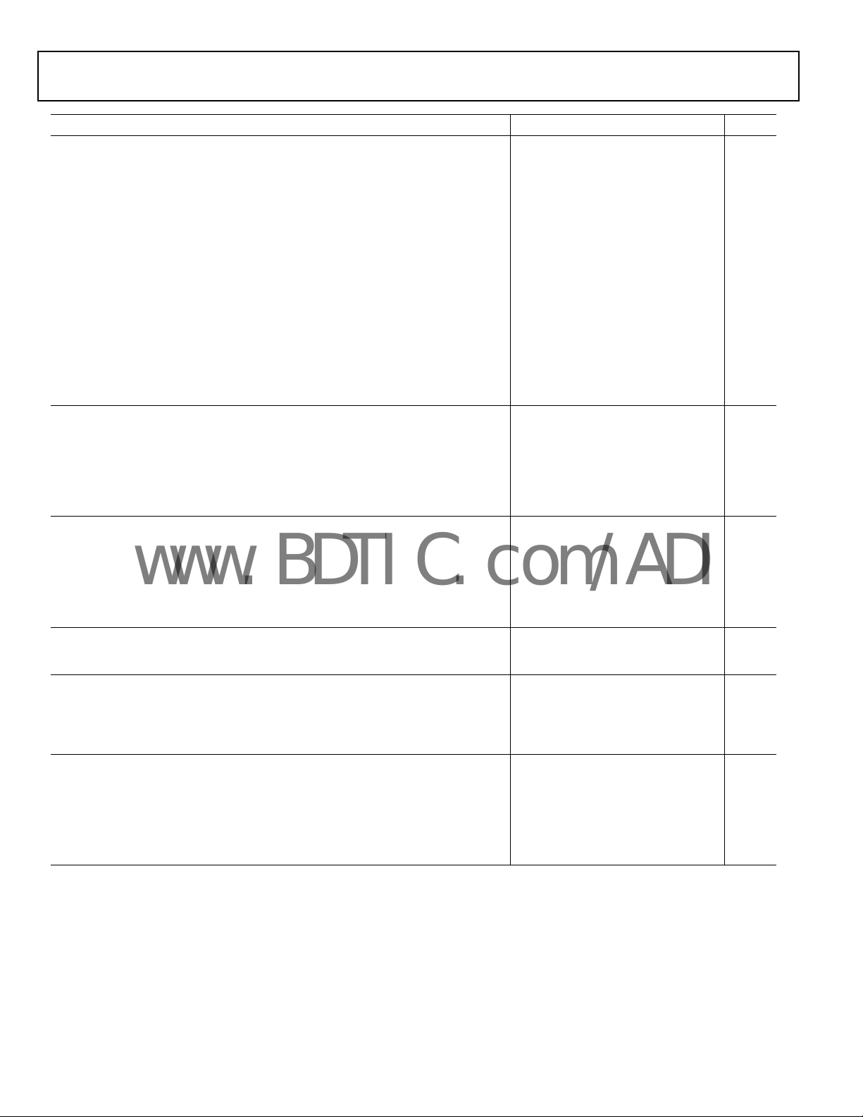
High Definition Audio
ADC0
ADC1
DAC1
DM_CLK
DM_1/2
DM_2
DIGITAL
MICROPHONE
MONO OUT
PORT A
PORT D
PORT F
AD1883
H
D
A
U
D
I
O
I
N
T
E
R
F
A
C
E
PORT B
PORT E
PORT C
DAC0
⌺
⌺
⌺
⌺
⌺
PCBEEP
HP
HP
⌺
DIGITAL
PCBEEP
S/PDIF-OUT
www.BDTIC.com/ADI
SoundMAX Codec
AD1883
FEATURES
Microsoft Vista Premium Logo for notebook
90+ dB audio outputs, 85 dB audio inputs
WLP 3.0 and 4.0
2 stereo headphone amplifiers
Internal 32-bit arithmetic for greater accuracy
Impedance and presence detection on all jacks
Full analog mixer with DAC inputs
3 independent microphone bias pins
Digital and analog PCBeep
3 general-purpose digital I/O (GPIO) pins
3.3 V analog supply voltage
1.7 V to 1.9 V or 3.3 V digital supply voltages
1.5 V or 3.3 V HD Audio link signaling voltage
Advanced power management modes
48-lead, RoHs compliant LFCSP_VQ package
192 kHz DACs/ADCs
2 independent stereo DAC/ADC pairs
Simultaneous record of 2 stereo channels
Simultaneous playback of 2 stereo channels
Independent 8 kHz, 11.025 kHz, 16 kHz, 22.05 kHz, 32 kHz,
44.1 kHz, 48 kHz, 88.2 kHz, 96 kHz, 176.4 kHz, and 192 kHz
sample rates
16-, 20-, and 24-bit resolution
Selectable stereo mixer on outputs
STEREO DIGITAL MICROPHONE INTERFACE
2 digital microphone channels
Supports 1 or 2 microphones per pin
Selectable clock rates of 1.5 MHz, 2.0 MHz, and 3.0 MHz
Mono and stereo array support
8 kHz, 11.025 kHz, 16 kHz, 22.05 kHz, 32 kHz, 44.1 kHz,
48 kHz, 88.2 kHz, 96 kHz, 176.4 kHz, and 192 kHz
sample rates
16-, 20-, and 24-bit resolution
S/PDIF OUTPUT
Supports 44.1 kHz, 48 kHz, 88.2 kHz, 96 kHz, 176.4 kHz, and
192 kHz sample rates
16-, 20-, and 24-bit data; PCM and AC3 formats
Digital PCM gain control
AUXILIARY PINS
Stereo CD/auxiliary I/O port with ground sense
Stereo auxiliary/dock I/O port
Mono out pin for internal speakers or telephony
Rev. 0
Information furnished by Analog Devices is believed to be accurate and reliable.
However, no responsibility is assumed by Analog Devices for its use, nor for any
infringements of patents or other rights of third parties that may result from its use.
Specifications subject to change without notice. No license is granted by implication
or otherwise under any patent or patent rights of Analog Devices. Trademarks and
registered trademarks are the property of their respective owners.
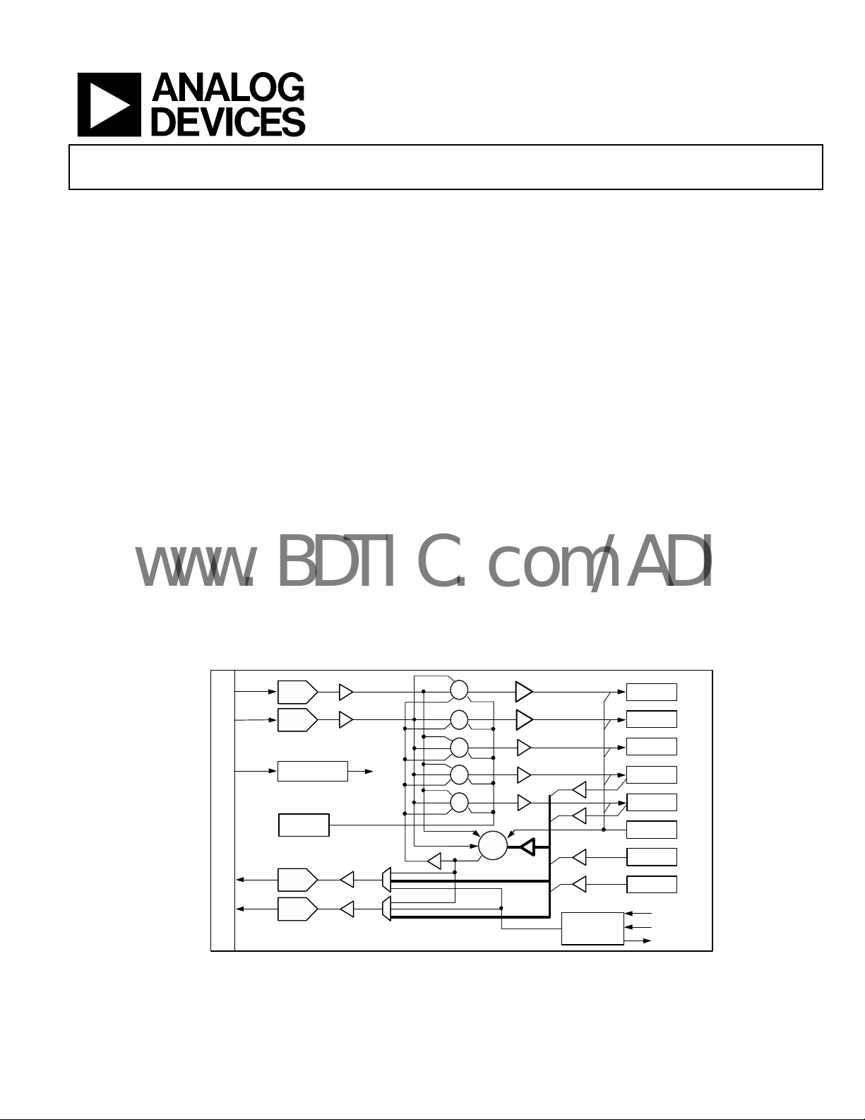
Figure 1. Functional Block Diagram
One Technology Way, P.O. Box 9106, Norwood, MA 02062-9106 U.S.A.
Tel: 781.329.4700 www.analog.com
Fax: 781.461.3113 ©2008 Analog Devices, Inc. All rights reserved.

AD1883
www.BDTIC.com/ADI
TABLE OF CONTENTS
Features ................................................................. 1
Revision History ...................................................... 2
General Description ................................................. 3
Additional Information .......................................... 3
Jack Configuration ................................................ 3
Specifications .......................................................... 4
Test Conditions .................................................... 4
Performance ........................................................ 4
General Specifications ............................................ 4
HD–Audio Link Specification .................................. 7
Power-Down States ............................................... 7
Absolute Maximum Ratings .................................... 8
ESD Caution ........................................................ 8
Environmental Conditions ...................................... 8
Pin Configuration and Function Descriptions ................. 9
Digital Microphone Interface Timing Specifications ....... 12
HD Audio Widgets ................................................ 14
HD Audio Parameters ............................................. 15
Widget Parameters ................................................. 16
Connection List ..................................................... 17
Default Configuration Bytes ..................................... 18
Outline Dimensions ............................................... 19
Ordering Guide ..................................................... 19
REVISION HISTORY
4/08—Rev 0. Initial version
Rev. 0 | Page 2 of 20 | April 2008
GENERAL DESCRIPTION
www.BDTIC.com/ADI
The AD1883 audio codec and SoundMAX® software provide
superior high definition audio quality that exceeds Vista Premium performance for notebooks. The AD1883 has two
192 kHz DAC pairs, two 192 kHz ADC pairs, a S/PDIF output, a
2-channel digital microphone interface, and digital and analog
PCBeep. These features make the AD1883 the right choice for
notebook PCs that meet Microsoft Vista Premium performance
as well as desktop PCs that meet Microsoft Vista Basic
performance.
The AD1883 is available in a 48-lead, RoHS compliant lead
frame chip scale package in both reels and trays. See Ordering
Guide on Page 19.
ADDITIONAL INFORMATION
This data sheet provides a general overview of the AD1883
SoundMAX codec’s architecture and functionality. Detailed
widget information is available in the AD1883 Programmers
Reference Manual. Please contact your local Analog Devices,
Inc., sales representative for more information.
JACK CONFIGURATION
The guidelines shown in Table 1 through Table 3 should be
used when selecting ports for particular functions.
AD1883
Table 1. Typical Desktop Configuration
Port Function
Port A Front Panel Headphone
Port B Front Panel Microphone
Port C Rear Panel Line-In/Microphone
Port D Rear Panel Line-Out/Headphone
S/PDIF Out Optical/RCA S/PDIF Output
Table 2. Typical Notebook Configuration
Port Function
Port A Headphone
Port B Microphone
Port C Internal Microphone
Port F Internal Stereo Speakers
S/PDIF Out Optical/RCA S/PDIF Output
Table 3. Typical Notebook Configuration with Dock
Interface
Port Function
Port A Headphone
Port B Microphone
Port C Internal Microphone
Port D Dock Line-Out/Headphone
Port E Dock Line-In/Microphone
Port F Internal Stereo Speakers
S/PDIF Out Optical/RCA S/PDIF Output
Rev. 0 | Page 3 of 20 | April 2008
AD1883
www.BDTIC.com/ADI
SPECIFICATIONS
TEST CONDITIONS
Parameter Test Condition
Tem pe ra tu re
Digital Supply
Analog Supply
MIC_BIAS_IN (via Low-Pass Filter)
Sample Rate F
Input Signal (Frequency Sine Wave)
Amplitude for THD + N
Analog Output Pass Band
DAC 10 kΩ Output Load: Line-Out Tests
ADC 0 dB Gain
S
PERFORMANCE
Parameter Min Typ Max Unit
Line-Out Drive (10 kΩ loads—DAC to Pin)
Total Harmonic Distortion (THD + N)
Dynamic Range (–60 dB in ref to f
Signal-to-Noise Ratio
Headphone Drive (32 Ω loads—DAC to Pin)
Total Harmonic Distortion (THD + N)
Dynamic Range (–60 dB in ref to f
Signal-to-Noise Ratio
Microphone/Line-In (Pin to ADC, Mic Boost = 0 dB)
Total Harmonic Distortion (THD + N)
Dynamic Range (–60 dB in ref to f
Signal-to-Noise Ratio
A-Weighted)
S
A-Weighted)
S
A-Weighted)
S
25°C
3.3 V
3.3 V
5.0 V
48 kHz
1008 Hz
–3.0 dB Full Scale
20 Hz to 20 kHz
32 Ω Output Load: Headphone Tests
–84
90
90
–74
90
90
–78
85
85
dB
dB
dB
dB
dB
dB
dB
dB
dB
GENERAL SPECIFICATIONS
Parameter Min Typ Max Unit
DIGITAL DECIMATION AND INTERPOLATION FILTERS–f
Pass Band 0 0.4 f
Pass-Band Ripple ±0.005 dB
Stop Band 0.6 f
Stop-Band Rejection –100 dB
Group Delay 20 1/f
Group Delay Variation over Pass Band 0 μs
ANALOG-TO-DIGITAL CONVERTERS
Resolution 24 Bits
Gain Error (Full-Scale Span Relative to Nominal Input Voltage) ±10 %
Interchannel Gain Mismatch (Difference of Gain Errors) ±0.2 ±0.5 dB
ADC Offset Error
ADC Crosstalk
Line Inputs (Input L, Ground R, Read R; Input R, Ground L, Read L) –85 dB
Line Inputs to Other –100 –80 dB
1
1
= 8 kHz to 192 kHz
S
Rev. 0 | Page 4 of 20 | April 2008
1
S
S
±5mV
Hz
Hz
S
AD1883
www.BDTIC.com/ADI
Parameter Min Typ Max Unit
DIGITAL-TO-ANALOG CONVERTERS
Resolution 24 Bits
Gain Error (Full-Scale Span Relative to Nominal Input Voltage)
Interchannel Gain Mismatch (Difference of Gain Errors) ±0.5 dB
Total Audible Out-of-Band Energy (Measured from 0.6 × fS to 20 kHz)
DAC Crosstalk (Input L, Zero R, Measure R_OUT; Input R, Zero L, Measure L_OUT)
DAC VOLUMES
Step Size 1.5 dB
Output Gain/Attenuation Range –58.5 0 dB
Mute Attenuation of 0 dB Fundamental
ADC VOLUMES
Step Size 1.5 dB
PGA Gain/Attenuation Range –58.5 +22.5 dB
ANALOG MIXER
Signal-to-Noise Ratio Input to Output—Ports B, C, E, or F to Port D Output 90 dB
Step Size: All Mixer Inputs –1.5 dB
Input Gain/Attenuation Range: All Mixer Inputs –34.5 +12.0 dB
ANALOG LINE LEVEL OUTPUTS
Full-Scale Output Voltage 1.0
Ports A, D, E, F, and Mono Out
ANALOG HP DRIVE OUTPUTS
Full-Scale Output Voltage 1.0
Ports A and D
ANALOG INPUTS
Input Voltages—Ports B, C, E, or F
Input Voltages—Microphone Boost
Amplifier, Ports B, C, or E
Input Impedance
PCBeep
Ports B, C, E (Mic Boost = 0 dB)
Port F
Input Capacitance
1
1
Output Impedance
External Load Impedance
Output Capacitance
External Load Capacitance 1000 pF
Output Impedance
External Load Impedance
Output Capacitance
External Load Capacitance
Mic Boost = 0 dB 1
Mic Boost = 10 dB 0.316
Mic Boost = 20 dB 0.1
Mic Boost = 30 dB 0.032
1
1
1
2.83
1
1
1
1
1
1
1
10 kΩ
2.83
32 Ω
–85 dB
–95 dB
–80 dB
190 Ω
15 pF
15 pF
2.83
0.894
0.283
0.089
23
150
45
57.5pF
±10 %
V rms
V p-p
V rms
V p-p
0.5 Ω
1000 pF
V rms
V p-p
V rms
V p-p
V rms
V p-p
V rms
V p-p
kΩ
kΩ
kΩ
Rev. 0 | Page 5 of 20 | April 2008
AD1883
www.BDTIC.com/ADI
Parameter Min Typ Max Unit
MICROPHONE BIAS
MIC_BIAS-B, MIC_BIAS-C
MIC_BIAS_IN (Pin 33) = 5 V or 3.3 V V
V
MIC_BIAS_IN (Pin 33) = 5 V V
V
MIC_BIAS_IN (Pin 33) = 3.3 V V
Setting = High-Z High-Z
REF
V
Setting = 0 V 0 V dc
REF
Setting = 50% 1.65 V dc
REF
Setting = 80% 3.7 V dc
REF
Setting = 100% 3.9 V dc
REF
Setting = 80% 2.86 V dc
REF
V
Setting = 100% 3.0 V dc
REF
MIC_BIAS-E (When Enabled as BIAS) V
Output Drive Current V
Setting = High-Z High-Z
REF
Setting = 0 V 0 V dc
V
REF
V
Setting = 50% 1.65 V dc
REF
Setting = 80% 2.86 V dc
V
REF
V
Setting = 100% 3.0 V dc
REF
Setting = 50%, 80%, or 100% 1.6 mA
REF
GPIO 0
Input Signal High (VIH)DV
Input Signal Low (V
Output Signal High (V
Output Signal Low (V
Input Leakage Current (Signal High) (I
Input Leakage Current (Signal Low) (I
)0DV
IL
) I
OH
)I
OL
IH
)–50μA
IL
= –500 μADV
OUT
= +1500 μA0 DV
OUT
) 150 nA
× 0.60 DV
IO
× 0.72 DV
IO
IO
× 0.24 V
IO
IO
× 0.10 V
IO
V
V
GPIO 1 and GPIO 2
Input Signal High (VIH)AV
Input Signal Low (V
Output Signal High (V
Output Signal Low (V
Input Leakage Current (Signal High) (I
Input Leakage Current (Signal Low) (I
)0AV
IL
)I
OH
)I
OL
IH
)–50μA
IL
= –500 μAAV
OUT
= +1500 μA0 AV
OUT
) 150 nA
× 0.60 AV
DD
× 0.72 AV
DD
DD
× 0.24 V
DD
DD
× 0.10 V
DD
V
V
DM Clock
Output Signal High (VOH)I
Output Signal Low (V
)I
OL
= –500 μAAV
OUT
= +1500 μA0 AV
OUT
× 0.72 AV
DD
DD
× 0.10 V
DD
V
DM_1/2 and DM_2
Input Signal High (V
Input Signal Low (V
)AV
IH
)0AV
IL
Input Leakage Current (Signal High) (I
Input Leakage Current (Signal Low) (I
) –150 nA
IH
)–50nA
IL
× 0.60 AV
DD
DD
× 0.24 V
DD
V
S/PDIF_Out
Input Signal High (V
Input Signal Low (V
Output Signal High (V
Output Signal Low (V
)DV
IH
)0DV
IL
) I
OH
)I
OL
Input Leakage Current (Signal High) (I
Input Leakage Current (Signal Low) (I
= –500 μADV
OUT
= +1500 μA0 DV
OUT
) 150 nA
IH
)–50μA
IL
× 0.60 DV
IO
× 0.72 DV
IO
IO
× 0.24 V
IO
IO
× 0.10 V
IO
V
V
Rev. 0 | Page 6 of 20 | April 2008

AD1883
www.BDTIC.com/ADI
Parameter Min Typ Max Unit
POWER SUPPLY
Analog (AV
Power Supply Range
Power Dissipation
Supply Current
Digital (DVDD) 3.3 V ± 10%
Power Supply Range
Power Dissipation
Supply Current
Digital (DV
Power Supply Range
Power Dissipation
Supply Current
Digital I/O (DV
Power Supply Range
Power Dissipation
Supply Current
Digital I/O (DV
Power Supply Range
Power Dissipation
Supply Current
Power Supply Rejection (Reference to fS 100 mV p-p Signal @ 1 kHz)1 80 dB
1
Guaranteed but not tested.
) 3.3 V ± 5%
DD
) 1.7 through 1.9 V ± 10%
CORE
) 3.3 V ± 10%
IO
) 1.5 V ± 5.5%
IO
3.13 3.30
75.9
23
2.97 3.30
141.9
43
1.615 1.70
61
36
2.97 3.30
3.3
1
1.418 1.50
0.08
0.05
3.46 V
mW
mA
3.63 V
mW
mA
1.995 V
mW
mA
3.63 V
mW
mA
1.583 V
mW
mA
HD AUDIO LINK SPECIFICATION
High definition audio signals comply with the High Definition
Audio Specification. Please refer to these specifications at
www.intel.com/standards/hdaudio.
POWER-DOWN STATES
Table 4. Power-Down States
Parameter ID
Function Node in D0, All Nodes Active 36 43 23 mA
Function Node in D3 15.75 17 1 mA
Function Node in D3
1
Codec in RESET
Individual Block Power Savings
DAC Pair Powered Down Saves (Each)
ADC Pair Powered Down Saves (Each)
Mixer Power Control (and Associated Amps) Saves
DM_CLK Powered Down Saves
MIC_BIAS Powered Down Saves
1
Maximum power saving mode; Register 0x31FD, Bit 4.
2
Test conditions: 30 pF load, 2.0 MHz frequency, 3.3 V A
3
Powering down the MIC_BIAS powers down all port MIC_BIAS pins. This disables all microphone bias circuits set to 100% or 50%, setting them to the high-Z state. The
0 V and high-Z states remain unaffected by the MIC_BIAS power state.
2
3
VDD.
Typ (1.7 V ) ID
VDD
Typ (3.3 V) IA
VDD
Typ Unit
VDD
7.5 7.5 1 mA
333mA
4.5
4.5
0
0
0
6
6
0
0
0
5
3
2
1
0.1
mA
mA
mA
mA
mA
Rev. 0 | Page 7 of 20 | April 2008

AD1883
ESD (electrostatic discharge) sensitive device.
Charged devices and circuit boards can discharge
without detection. Although this product features
patented or proprietary protection circuitry, damage
may occur on devices subjected to high energy ESD.
Therefore, proper ESD precautions should be taken to
avoid
performance degradation or loss of functionality.
www.BDTIC.com/ADI
ABSOLUTE MAXIMUM RATINGS
Stresses greater than those listed below may cause permanent
damage to the device. This is a stress rating only; functional
operation of the device at these or any other conditions above
those indicated in the operational section of this specification is
not implied. Exposure to absolute maximum rating conditions
for extended periods may affect device reliability.
Parameter Rating
Digital (DV
Digital (DV
Digital I/O (DV
Analog (AV
Input Current (Except Supply Pins) ±10.0 mA
Analog Input Voltage (Signal Pins) –0.30 V to AVDD +0.3 V
Digital Input Voltage (Signal Pins) –0.30 V to DV
Ambient Temperature (Operating) 0°C to +70°C
Storage Temperature –65°C to +150°C
) –0.30 V to +3.65 V
DD
) –0.30 V to +2.10 V
CORE
) –0.30 V to +3.65 V
IO
) –0.30 V to +3.65 V
DD
+0.3 V
IO
ESD CAUTION
ENVIRONMENTAL CONDITIONS
Ambient Temperature Rating:
T
= T
AMB
T
CASE
PD = power dissipation in W
= thermal resistance (case-to-ambient)
θ
CA
θ
= thermal resistance (junction-to-ambient)
JA
θ
= thermal resistance (junction-to-case)
JC
All measurements per EIA-JESD51 with 2S2P test board per
EIA-JESD51-7.
Package θ
LFCSP_VQ 47 15 32 °C/W
– (PD × θCA)
CASE
= case temperature in °C
JA
θ
JC
θ
CA
Unit
Rev. 0 | Page 8 of 20 | April 2008

PIN CONFIGURATION AND FUNCTION DESCRIPTIONS
1
2
3
4
5
6
7
8
9
10
11
12
242313 14 15 16 17 18 19 20 21 22
34
33
36
35
25
26
27
28
29
30
31
32
44 434748 4546 373839404142
AD1883JCP
TOP VIEW
(NotTo Scale)
DV
CORE
DM_1/2
DV
IO
DM_2
SDATA_OUT
BIT_CLK
DV
SS
SDATA_IN
DV
DD
SYNC
RESET
PCBEEP
PORT-D_R
PORT-D_L
P
O
R
T
-
C
_
R
P
O
R
T
-
C
_
L
P
O
R
T
-
B
_
R
P
O
R
T
-
E
_
L
P
O
R
T
-
F
_
R
P
O
R
T
-
F
_
L
P
O
R
T
-
B
_
L
P
O
R
T
-
E
_
R
C
D
_
G
N
D
(
P
O
R
T
F
)
S
E
N
S
E
_
A
/
S
R
C
_
B
SENSE_B/SRC_A
P
O
R
T
-
A
_
L
P
O
R
T
-
A
_
R
E
A
P
D
/
G
P
I
O
_
0
R
E
S
E
R
V
E
D
(
N
C
)
A
V
D
D
D
M
_
C
L
K
R
E
S
E
R
V
E
D
(
N
C
)
R
E
S
E
R
V
E
D
(
N
C
)
A
V
S
S
S
P
D
I
F
_
O
U
T
R
E
S
E
R
V
E
D
(
N
C
)
MIC_BIAS_IN
MIC_BIAS-B
MIC_BIAS-C
GPIO_2
MIC_BIAS-E/GPIO_1
MONO_OUT
AV
DD
AV
SS
VREF_FLT
R
E
S
E
R
V
E
D
(
N
C
)
R
E
S
E
R
V
E
D
(
N
C
)
R
E
S
E
R
V
E
D
(
N
C
)
www.BDTIC.com/ADI
AD1883
Figure 2. AD1883 48-Lead Package and Pinout
Rev. 0 | Page 9 of 20 | April 2008

AD1883
www.BDTIC.com/ADI
Table 5. Pin Function Descriptions
Mnemonic Pin No. I/O Description
DIGITAL INTERFACE
SDATA_OUT
BIT_CLK
SDATA_IN
SYNC
RESET
DIGITAL I/O and EAPD
DM_1/2
DM_2
DM_CLK
GPIO_2
MIC_BIAS-E/GPIO_1
EAPD/GPIO_0
SPDIF_OUT
JACK SENSE
SENSE_A/SRC_B
SENSE_B/SRC_A
ANALOG I/O
PCBEEP
PORT-E_L
PORT-E_R
PORT-F_L
PORT-F_R
CD_GND (PORT F)
PORT-B_L
PORT-B_R
PORT-C_L
PORT-C_R
MONO_OUT
PORT-D_L
PORT-D_R
PORT-A_L
PORT-A_R
The symbols used in this table are defined as: I = input, O = output, LI = line level input, LO = line level output, HP = output capable of driving
headphone load, MIC = input supports microphones with MIC bias and boost amplifier.
5
6
8
10
11
2
4
46
30
31
47
48
13
34
12
14
15
16
17
19
21
22
23
24
32
35
36
39
41
I
I
I/O
I
I
I
I
O
I/O
I/O
I/O
O
I/O
I/O
LI
LI, MIC, LO
LI, MIC, LO
LI, LO
LI, LO
I
LI, MIC
LI, MIC
LI, MIC
LI, MIC
LO
HP, LO
HP, LO
HP, LO
HP, LO
Link Serial Data Output. AD1883 input stream. Clocked on both edges of the
BIT_CLK.
Link Bit Clock. 24.000 MHz serial data clock.
Link Serial Data Input. AD1883 output stream clocked only on one edge of BIT_CLK.
Link Frame Sync.
Link Reset. AD1883 master hardware reset.
Digital microphone 1 and 2 Inputs (for Biphase Microphones), or Digital Microphone
1 Input (for Single-phase Microphones).
Digital Microphone 2 Input (for Single-phase Microphones).
Clock to Drive External Digital Microphones.
General-Purpose Input/Output Pins. Digital signals used to control or sense external
circuitry.
Microphone Bias for Port E/General-Purpose Input/Output. Capable of high-Z, 1.65 V,
and 2.86 V. Pin 31 shares functionality between MIC_BIAS_E (default) and GPIO_1.
These functions are mutually exclusive and the MIC_BIAS function takes priority over
the GPIO function.
EAPD/General-Purpose Input/Output Pin. Pin 47 shares functionality between
GPIO_0 and EAPD. These functions are mutually exclusive and the EAPD function
takes priority over the GPIO function. By default, the pin is in a high-Z state. External
resistors should be used to ensure the proper circuit state when this pin is in high-Z.
Supports S/PDIF Output.
Jack Sense A-D Input/Sense B drive.
Jack Sense E-F Input/Sense A drive.
Monaural Input from System for Analog PCBeep.
Auxiliary Input/Output Left Channel.
Auxiliary Input/Output Right Channel.
Auxiliary Input/Output Left Channel.
Auxiliary Input/Output Right Channel.
CD Audio Analog Ground Reference. Must be connected to AGND via a 0.1 μF
capacitor if not in use as CD_GND. MUST always be ac-coupled.
Front Panel Stereo MIC/Line-In.
Front Panel Stereo MIC/Line-In.
Rear Panel Stereo MIC/Line-In.
Rear Panel Stereo MIC/Line-In.
Monaural Output to Internal Speaker or Telephony Subsystem Speakerphone.
Rear Panel Headphone/Line-Out.
Rear Panel Headphone/Line-Out.
Front Panel Headphone/Line-Out.
Front Panel Headphone/Line-Out.
Rev. 0 | Page 10 of 20 | April 2008

AD1883
www.BDTIC.com/ADI
Table 5. Pin Function Descriptions (Continued)
Mnemonic Pin No. I/O Description
FILTER/MIC_BIAS
VREF _FLT
MIC_BIAS-B
MIC_BIAS-C
MIC_BIAS_IN
5.0 V or 3.3 V
POWER AND GROUND
DV
1.7 V to 1.9 V or
CORE
FILTER
1.5 V or 3.3 V 3 I Link Digital I/O Voltage Reference. 3.3 V ± 10% or 1.5 V ± 5.5%
DV
IO
DV
SS
1.7 V to 1.9 V or 3.3 V 9 I Digital Supply Voltage 3.3 V ± 10%. This is regulated down to DV
DV
DD
AV
3.3 V 25, 38 I CAUTION: DO NOT APPLY 5 V TO THESE PINS! Analog Supply Voltage 3.3 V ± 5%.
DD
AV
SS
The symbols used in this table are defined as: I = input, O = output, LI = line level input, LO = line level output, HP = output capable of driving
headphone load, MIC = input supports microphones with MIC bias and boost amplifier.
27
28
29
33
1 I/O CAUTION: DO NOT APPLY 3.3 V TO THIS PIN! Filter connection for internal core
7 I Digital Supply Return (Ground).
26, 42 I Analog Supply Return (Ground). AVSS should be connected to DVSS using a
O
O
O
I
Voltage Reference Filter.
Switchable Microphone Bias. For use with Port B (Pins 21, 22).
Switchable Microphone Bias. For use with Port C (Pins 23, 24).
Both MIC bias pins are capable of:
High-Z, 0 V, 1.65 V, 3.7 V, and 3.9 V (with 5.0 V on Pin 33)
High-Z, 0 V, 1.65 V, 2.86 V, and 3.0 V (with 3.3 V on Pin 33).
Source Power for Microphone Bias Boost Circuitry.
Connect this pin to 5.0 V via a low-pass filter. When connected this way the AD1883 is
capable of providing 3.9 V as a mic bias to all of the mic bias pins (except on Pin 31).
If 5 V is not available, connect this pin to 3.3 V (AV
voltage regulator.
If Pin 9 is connected to 3.3V DVDD, this pin must be connected to filter caps: 10μF,
1.0 μF, and 0 .1 μF connected in parallel between Pin 1 and DVSS (Pin 7). Direct, filtered
1.7 V to 1.9 V DVDD can be applied to Pin 1 to lower the digital power requirements.
Pin 9 MUST be connected to Pin 1 in this case.
supply the internal digital core internal to the AD1883. Direct, filtered 1.7 V to 1.9 V
may be applied to Pin 1 to lower the digital power requirements. Pin 9 MUST be
DV
DD
connected to Pin 1 in this case.
Note: AV
audio performance.
conductive trace under, or close to, the AD1883.
supplies should be well regulated and filtered as supply noise degrades
DD
) via a low-pass filter.
DD
CORE
on Pin 1 to
Rev. 0 | Page 11 of 20 | April 2008

AD1883
DM_CLK
t
1
t
2
t
3
DM_1/2
t
0
DATA VALID
t
4
DM_CLK
t
1
t
2
t
3
DM_2
t
0
DATA VALID
t
4
www.BDTIC.com/ADI
DIGITAL MICROPHONE INTERFACE TIMING SPECIFICATIONS
The digital microphone interface can support one or two digital
microphones using two or three codec pins. Both uniplex (one
microphone per data pin) and multiplex (two microphones
sharing the same data pin) are supported. The timing for these
configurations is shown in Table 6 and Figure 3, Figure 4 and
Figure 5. The interface can generate a microphone clock at
1.5 MHz, 2.0 MHz, or 3.0 MHz to suit quality and power
requirements.
Table 6. Microphone Timing Parameters
Parameter Description Min Typ Max Unit
Timing Requirements
t
0
t
0
t
0
t
1
t
2
t
3
t
4
DM_CLK (1.5 MHz) Period
Duty Cycle
DM_CLK (2.0 MHz) Period
Duty Cycle
DM_CLK (3.0 MHz) Period
Duty Cycle
667
50/50
500
50/50
333
50/50
ns
%
ns
%
ns
%
DM_CLK Rise Time 5 ns
DM_CLK Fall Time 5ns
Data Setup to DM_CLK Edge 10 ns
Data Hold from DM_CLK Edge 5 ns
Figure 3. Uniplex Microphone Timing
Figure 4. DM_2 Uniplex Microphone Timing
Rev. 0 | Page 12 of 20 | April 2008

Figure 5. Multiplex Microphone Timing
DM_CLK
t
1
t
2
t
3
DM_1/2
t
0
LEFT DATA VALID
RIGHT DATA VALID LEFT DATA VALID
t
4
t
3
t
4
www.BDTIC.com/ADI
AD1883
Rev. 0 | Page 13 of 20 | April 2008

AD1883
www.BDTIC.com/ADI
HD AUDIO WIDGETS
Table 7. HD Audio Widgets
Node ID Name Type ID Type Description
0x00 ROOT x Root Device identification
0x01 FUNCTION x Function Designates this device as an audio codec
0x02 S/PDIF DAC 0 Audio Output S/PDIF digital stream output interface
0x03 DAC_0 0 Audio Output Stereo headphone channel digital/audio converter
0x04 DAC_1 0 Audio Output Stereo front channel digital/audio converter
0x07 Port A Mixer 2 Audio Mixer Mixes the DAC_(0, 1) and analog mixer output to drive Port A
0x08 ADC_0 1 Audio Input Stereo record Channel 0 audio/digital converters
0x09 ADC_1 1 Audio Input Stereo record Channel 1 audio/digital converters
0x0A Port D Mixer 2 Audio Mixer Mixes the DAC_1 and analog mixer output to drive Port D
0x0B Port F Mixer 2 Audio Mixer Mixes the DAC_(0, 1) and analog mixer output to drive Port F
0x0C ADC Selector 0 3 Audio Selector Selects and amplifies/attenuates the input to ADC_0
0x0D ADC Selector 1 3 Audio Selector Selects and amplifies/attenuates the input to ADC_1
0x0E Mono Out Selector 3 Audio Selector Selects the mono out DAC_(0, 1)
0x0F Port F Out Selector 3 Audio Selector Selects the Port F DAC_(0, 1)
0x10 Digital Beep 7 Beep Generator Internal digital PCBeep signal
0x11 Port A (Headphone) 4 Pin Complex Headphone jack pins
0x12 Port D (Line Out) 4 Pin Complex Line out jack pins
0x13 Mono Out 4 Pin Complex Monaural output pin (internal speakers or telephony system)
0x14 Port B (Mic In) 4 Pin Complex Microphone in jack pins
0x15 Port C (Line In) 4 Pin Complex Line in jack pins
0x16 Port F (Aux In/Out) 4 Pin Complex Auxiliary I/O pins
0x17 Dig Microphone 4 Pin Complex Digital microphone input pin
0x19 Mixer Power-Down 5 Power Widget Powers down the analog mixer and associated amps
0x1A Analog PCBeep 4 Pin Complex External analog PCBeep signal input
0x1B S/PDIF-Out 4 Pin Complex S/PDIF output pin
0x1C Port E (Dock I/O) 4 Pin Complex Analog dock I/O pins
0x1D V
0x1E Mono Out Mixer 2 Audio Mixer Mixes the DAC_(0, 1) and analog mixer output to drive mono out
0x1F Stereo Mix-Down 2 Audio Mixer Mixes the stereo L/R channels to drive mono output
0x20 Analog Mixer 2 Audio Mixer Mixes individually gainable analog inputs
0x21 Mixer Output Atten 3 Audio Selector Attenuates the analog mixer output to drive the port mixers
0x22 Port A Out Selector 3 Audio Selector Selects the Port A DAC_(0, 1)
0x23 Port E Out Selector 3 Audio Selector Selects the Port E DAC_(0, 1)
0x24 Port E Mixer 2 Audio Mixer Mixes the DAC_(0, 1) and analog mixer output to drive Port E
0x25 Port E Mic Boost 3 Audio Selector 0 dB, 10 dB, 20 dB, or 30 dB gain boost for Port E
0x26 BIAS Power-Down F Vendor Defined Powers down the internal MIC_BIAS_FILT and all MIC_BIAS pins
1
All node IDs (NIDs) are sequential in the codec. Any NIDs missing from this table are vendor defined.
Power-Down F Vendor Defined Powers down the V
REF
1
circuitry
REF
Rev. 0 | Page 14 of 20 | April 2008

HD AUDIO PARAMETERS
www.BDTIC.com/ADI
Table 8. Root and Function Node Parameters
AD1883
Vendor ID
Node ID Name
0x00 ROOT 0x11D4 1883 0x0010 0200 0x0001 0001
0x01 FUNCTION 0x0002 0029 0x0000 0001 0x0001 0C0C 0x4000 0003
1
Subject to change with silicon stepping.
Table 9. Subsystem ID
Node ID Name Type Value
0x01 FUNCTION Function 0xBFD4 0000 0xBFD4 0x00 0x00
00
Revision ID
1
02
Sub Node Count04Func. Group Type05Audio F.G. Caps08GPIO Caps
11
31:16
SSID
15:8
SKU
7:0
ASM ID
Rev. 0 | Page 15 of 20 | April 2008

AD1883
www.BDTIC.com/ADI
WIDGET PARAMETERS
Table 10. Widget Parameters
Widget
Node
Capabilities
ID
0x09
0x01 0x0000 04C0 0x000E 07FF 0x0000 0001 0x8000 0000 0x0000 0009 0x0005 2727
0x02 0x0003 0211 0x000E 07E0 0x0000 0005 0x0000 0000
0x03 0x0000 0405 0x000E 07FF 0x0000 0001 0x0000 0000 0x0000 0009 0x0005 2727
0x04 0x0000 0405 0x000E 07FF 0x0000 0001 0x0000 0000 0x0000 0009 0x0005 2727
0x07 0x0020 0103 0x8000 0000 0x0000 0002
0x08 0x0010 0501 0x000E 07FF 0x0000 0001 0x0000 0001 0x0000 0009
0x09 0x0010 0501 0x000E 07FF 0x0000 0001 0x0000 0001 0x0000 0009
0x0A 0x0020 0103 0x8000 0000 0x0000 0002
0x0B 0x0020 0103 0x8000 0000 0x0000 0002
0x0C 0x0030 010D 0x0000 0006 0x8005 3627
0x0D 0x0030 010D 0x0000 0006 0x8005 3627
0x0E 0x0030 0101 0x0000 0002
0x0F 0x0030 0101 0x0000 0002
0x10 0x0070 000C 0x0000 0000 0x800B 0F0F
0x11 0x0040 018D 0x0000 001F 0x0000 0001 0x8000 0000
0x12 0x0040 058D 0x0001 001F 0x0000 0001 0x0000 0009 0x8000 0000
0x13 0x0040 050C 0x0001 0010 0x0000 0001 0x0000 0009 0x8005 1F1F
0x14 0x0040 008B 0x0000 3727 0x0027 0300 0x0000 0000
0x15 0x0040 008B 0x0000 3727 0x0027 0300 0x0000 0000
0x16 0x0040 058D 0x0001 0037 0x0000 0001 0x0000 0009 0x8000 0000
0x17 0x0040 020B 0x0000 0020 0x0017 0300 0x0000 0000
0x19 0x0050 0500 0x0000 0002 0x0000 0009
0x1A 0x0040 0000 0x0000 0020 0x0000 0000
0x1B 0x0040 038D 0x0000 0014 0x0000 0001 0x8005 2727
0x1C 0x0040 018D 0x0000 3737 0x0000 0001 0x8000 0000
0x1D 0x00F0 0100 0x0000 000A
0x1E 0x0020 0103 0x8000 0000 0x0000 0002
0x1F 0x0020 0100 0x0000 0001
0x20 0x0020 010B 0x8005 1F17 0x0000 0007
0x21 0x0030 010D 0x0000 0001 0x8005 1F1F
0x22 0x0030 0101 0x0000 0002
0x23 0x0030 0101 0x0000 0002
0x24 0x0020 0103 0x8000 0000 0x0000 0002
0x25 0x0030 010D 0x0000 0001 0x0027 0300
0x26 0x00F0 0100 0x0000 0003
PCM Size,
Rate
0x0A
Stream
Formats
0x0B
Pin
Capabilities
0x0C
Input Amp
Capabilities
0x0D
Con. List
Length
0x0E
Power States
0x0F
Output Amp
Capabilities
0x12
Rev. 0 | Page 16 of 20 | April 2008

CONNECTION LIST
www.BDTIC.com/ADI
Table 11. Connection List
AD1883
Node
ID
[0–3] [4–7] [8–11] NID R
0x02
0x03
0x04
0x07 0x0000 2122 0x22 0x21
0x08 0x0000 000C 0x0C
0x09 0x0000 000D 0x0D
0x0A 0x0000 2104 0x04 0x21
0x0B 0x0000 210F 0x0F 0x21
0x0C 0x2016 1514 0x0000 1725 0x14 0x15 0x16 0x20 0x25 0x17
0x0D 0x2016 1514 0x0000 1725 0x14 0x15 0x16 0x20 0x25 0x17
0x0E 0x0000 0403 0x03 0x04
0x0F 0x0000 0403 0x03 0x04
0x10
0x11 0x0000 0007 0x07
0x12 0x0000 000A 0x0A
0x13 0x0000 001F 0x1F
0x14
0x15
0x16 0x0000 000B 0x0B
0x17
0x19 0x0000 2120 0x20 0x21
0x1A
0x1B 0x0000 0002 0x02
0x1C 0x0000 0024 0x24
0x1D 0x118F 0A07 0x1C1A 1996 0x0000 A61E 0x07 0x0A 1 0x0F 0x11 1 0x16 0x19 0x1A 0x1C 0x1E 1 0x26
0x1E 0x0000 210E 0x0E 0x21
0x1F 0x0000 001E 0x1E
0x20 0x1A16 1514 0x004 0325 0x14 0x15 0x16 0x1A 0x25 0x03 0x04
0x21 0x0000 0020 0x20
0x22 0x0000 0403 0x03 0x04
0x23 0x0000 0403 0x03 0x04
0x24 0x0000 2123 0x23 0x21
0x25 0x0000 001C 0x1C
0x26 0x001C 1514 0x14 0x15 0x1C
1
R = the MS bit of any node ID indicates a 2-tuple NID pair delineating a continuous range of nodes. If the MS bit is set (=1), that list entry forms a range of entries from the
previous NID to the current NID. For additional information, see chapter 7.1.2, “Node Addressing” in the High Definition Audio Specification.
Connections 0123456789
1
NIDRNIDRNIDRNIDRNIDRNIDRNIDRNIDRNID
Rev. 0 | Page 17 of 20 | April 2008

AD1883
www.BDTIC.com/ADI
DEFAULT CONFIGURATION BYTES
Table 12. Default Configuration Bytes
31:30 29:28 27:24 23:20
Location
Connectivity
0x11 Port A (Headphone) 0x0321 40F0 Jack External Left HP Out
0x12 Port D (Line Out) 0x2121 4010 Jack Separate Rear HP Out
0x13 Mono Out 0x9017 01F0 Fixed Internal N/A Speaker
0x14 Port B (Mic In) 0x03A1 90F0 Jack External Left Mic In
0x15 Port C (Line In) 0xB7A7 0121 Fixed Other Special 1 Mic In
0x16 Port F (Aux In/Out) 0x9933 012E Fixed Internal Special 3 CD
0x17 Dig Mic Pin 0x97A6 01F0 None Internal Special 1 Mic In
0x1A Analog PCBeep 0x90F3 01F0 Fixed Internal N/A other
0x1B S/PDIF Out 0x0145 10F0 Jack External Rear SPDIF Out
0x1C Port E (Dock I/O) 0x21A1 9020 Jack Separate Rear Mic In
Table 12. Default Configuration Bytes (Continued)
19:16 15:12 8 7:4 3:0
Node ID Name Value Conn Type Color JD OVRD Def Assn. Seq.
0x11 Port A (Headphone) 0x0321 40F0 1/8” Jack Green 0 0xF 0x0
0x12 Port D (Line Out) 0x2121 4010 1/8” Jack Green 0 0x1 0x0
0x13 Mono Out 0x9017 01F0 Other Analog Unknown 1 0xF 0x0
0x14 Port B (Mic In) 0x03A1 90F0 1/8” Jack Pink 0 0xF 0x0
0x15 Port C (Line In) 0xB7A7 0121 Other Analog Unknown 1 0x2 0x1
0x16 Port F (Aux In/Out) 0x9933 012E ATAPI Unknown 1 0x2 0xE
0x17 Dig Mic Pin 0x97A6 01F0 Other Digital Unknown 1 0xF 0x0
0x1A Analog PCBeep 0x90F3 01F0 ATAPI Unknown 1 0xF 0x0
0x1B S/PDIF Out 0x0145 10F0 Optical Black 0 0xF 0x0
0x1C Port E (Dock I/O) 0x21A1 9020 1/8” Jack Pink 0 0x2 0x0
Def. DeviceNode ID Name Value Chassis Position
Rev. 0 | Page 18 of 20 | April 2008

OUTLINE DIMENSIONS
PIN 1
INDICATOR
TOP
VIEW
6.75
BSC SQ
7.00
BSC SQ
1
48
12
13
37
36
24
25
5.25
5.10 SQ
4.95
0.50
0.40
0.30
0.30
0.23
0.18
0.50 BSC
12° MAX
0.20 REF
0.80 MAX
0.65 TYP
1.00
0.85
0.80
5.50
REF
0.05 MAX
0.02 NOM
0.60 MAX
0.60 MAX
PIN 1
INDICATOR
COPLANARITY
0.08
SEATING
PLANE
0.25 MIN
EXPOSED
PAD
(BOTTOM VIEW)
COMPLIANT TO JEDEC STANDARDS MO-220-VKKD-2
www.BDTIC.com/ADI
AD1883
Figure 6. 48-Lead Lead Frame Chip Scale Package [LFCSP_VQ]
7 mm x 7 mm Body, Very Thin Quad
(CP-48-1)
Dimensions shown in millimeters
ORDERING GUIDE
Model Temperature Range Package Description Package Option
AD1883JCPZ
AD1883JCPZ-RL
1
Z = RoHS Compliant Part.
1
1
0°C to 70°C 48-Lead LFCSP_VQ CP-48-1
0°C to 70°C 48-Lead LFCSP_VQ, 13” Tape and Reel CP-48-1
Rev. 0 | Page 19 of 20 | April 2008

AD1883
www.BDTIC.com/ADI
©2008 Analog Devices, Inc. All rights reserved. Trademarks and
registered trademarks are the property of their respective owners.
D07397-0-4/08(0)
Rev. 0 | Page 20 of 20 | April 2008
 Loading...