

Single-Supply
a
FEATURES
Single 5 V Power Supply
Single-Ended Dual-Channel Analog Inputs
92 dB (Typ) Dynamic Range
90 dB (Typ) S/(THD+N)
0.006 dB Decimator Passband Ripple
Fourth-Order, 64-Times Oversampling ⌺⌬ Modulator
Three-Stage, Linear-Phase Decimator
256 ⴛ F
Less than 100 W (Typ) Power-Down Mode
Input Overrange Indication
On-Chip Voltage Reference
Flexible Serial Output Interface
28-Lead SOIC Package
APPLICATIONS
Consumer Digital Audio Receivers
Digital Audio Recorders, Including Portables
Multimedia and Consumer Electronic Equipment
Sampling Music Synthesizers
Digital Karaoke Systems
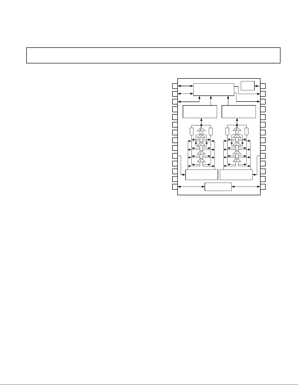
PRODUCT OVERVIEW
The AD1877 is a stereo, 16-bit oversampling ADC based on
Sigma Delta (∑∆) technology intended primarily for digital
audio bandwidth applications requiring a single 5 V power supply.
Each single-ended channel consists of a fourth-order one-bit
noise shaping modulator and a digital decimation filter. An onchip voltage reference, stable over temperature and time, defines
the full-scale range for both channels. Digital output data from
both channels are time-multiplexed to a single, flexible serial
interface. The AD1877 accepts a 256 × F
clock (F
port “master” and “slave” modes. In slave mode, all clocks must
be externally derived from a common source.
Input signals are sampled at 64 × F
switched-capacitors, eliminating external sample-and-hold amplifiers and minimizing the requirements for antialias filtering at the
input. With simplified antialiasing, linear phase can be preserved
across the passband. The on-chip single-ended to differential signal
converters save the board designer from having to provide them
externally. The AD1877’s internal differential architecture provides
increased dynamic range and excellent power supply rejection
characteristics. The AD1877’s proprietary fourth-order differential switched-capacitor ∑∆ modulator architecture shapes the
*Protected by U.S. Patent Numbers 5055843, 5126653, and others pending.
or 384 ⴛ FS Input Clock
S
CD-R, DCC, MD and DAT
or a 384 × FS input
is the sampling frequency) and operates in both serial
S
S
onto internally buffered
S
16-Bit ⌺⌬ Stereo ADC
AD1877*
FUNCTIONAL BLOCK DIAGRAM
LRCK
WCLK
BCLK
DV
DD
DGND1
RDEDGE
S/M
384/256
AV
VINL
CAPL1
CAPL2
AGNDL
V
REF
1
2
3
THREE-STAGE FIR
4
1
5
6
7
8
9
DD
10
11
12
DIFFERENTIAL INPUT
13
L
14
SERIAL OUTPUT
DECIMATION
FILTER
D
A
C
SINGLE TO
CONVERTER
INTERFACE
D
A
C
VOLTAGE
REFERENCE
THREE-STAGE FIR
D
A
C
DIFFERENTIAL INPUT
CONVERTER
DIVIDER
DECIMATION
FILTER
SINGLE TO
AD1877
CLOCK
D
A
C
one-bit comparator’s quantization noise out of the audio passband. The high order of the modulator randomizes the modulator
output, reducing idle tones in the AD1877 to very low levels.
Because its modulator is single-bit, AD1877 is inherently
monotonic and has no mechanism for producing differential
linearity errors.
The input section of the AD1877 uses autocalibration to correct
any dc offset voltage present in the circuit, provided that the inputs
are ac coupled. The single-ended dc input voltage can swing
between 0.7 V and 3.8 V typically. The AD1877 antialias input
circuit requires four external 470 pF NPO ceramic chip filter
capacitors, two for each channel. No active electronics are
needed. Decoupling capacitors for the supply and reference pins
are also required.
The dual digital decimation filters are triple-stage, finite impulse
response filters for effectively removing the modulator’s high
frequency quantization noise and reducing the 64 × F
output data rate to an F
word rate. They provide linear phase
S
and a narrow transition band that properly digitizes 20 kHz signals
at a 44.1 kHz sampling frequency. Passband ripple is less than
0.006 dB, and stopband attenuation exceeds 90 dB.
(Continued on Page 6)
CLKIN
28
TAG
27
SOUT
26
DV
25
DD
24
DGND2
23
RESET
22
MSBDLY
21
RLJUST
20
AGND
VINR
19
CAPR1
18
CAPR2
17
AGNDR
16
V
15
REF
single-bit
S
2
R
REV. A
I
Information furnished by Analog Devices is believed to be accurate and
reliable. However, no responsibility is assumed by Analog Devices for its
use, nor for any infringements of patents or other rights of third parties
which may result from its use. No license is granted by implication or
otherwise under any patent or patent rights of Analog Devices.
One Technology Way, P.O. Box 9106, Norwood, MA 02062-9106, U.S.A.
Tel: 781/329-4700 World Wide Web Site: http://www.analog.com
Fax: 781/326-8703 © Analog Devices, Inc., 2000

AD1877–SPECIFICATIONS
TEST CONDITIONS UNLESS OTHERWISE NOTED
Supply Voltages 5.0 V
Ambient Temperature 25 °C
Input Clock (F
Input Signal 991.768 Hz
Measurement Bandwidth 23.2 Hz to 19.998 kHz
Load Capacitance on Digital Outputs 50 pF
Input Voltage HI (V
Input Voltage LO (V
Master Mode, Data I
Device Under Test (DUT) bypassed and decoupled as shown in Figure 3.
DUT is antialiased and ac coupled as shown in Figure 2. DUT is calibrated.
Values in bold typeface are tested, all others are guaranteed but not tested.
ANALOG PERFORMANCE
Resolution 16 Bits
Dynamic Range (20 Hz to 20 kHz, –60 dB Input)
Without A-Weight Filter 87 92 dB
With A-Weight Filter 90 94 dB
Signal to (THD + Noise) 86.5 90 dB
Signal to THD 92 94 dB
Analog Inputs
Single-Ended Input Range (± Full Scale)* V
Input Impedance at Each Input Pin 32 kΩ
V
REF
DC Accuracy
Gain Error ±0.5 ⴞ2.5 %
Interchannel Gain Mismatch 0.01 dB
Gain Drift 115 ppm/°C
Midscale Offset Error (After Calibration) ± 3 ⴞ20 LSBs
Midscale Drift 15 ppm/°C
Crosstalk (EIAJ Method) –90 –99 dB
*VIN p-p = V
REF
) [256 × FS] 12.288 MHz
CLKIN
–0.5 dB Full Scale
) 2.4 V
IH
) 0.8 V
IL
2
S-Justified (Refer to Figure 14).
× 1.333.
Min Typ Max Unit
– 1.55 V
REF
REF
V
+ 1.55 V
REF
2.05 2.25 2.55 V
–2–
REV. A

AD1877
DIGITAL I/O
Min Typ Max Unit
Input Voltage HI (V
Input Voltage LO (V
Input Leakage (I
Input Leakage (I
Output Voltage HI (V
Output Voltage LO (V
Input Capacitance 15 pF
DIGITAL TIMING (Guaranteed over 0°C to 70°C, DVDD = AVDD = 5 V ± 5%. Refer to Figures 17–19.)
t
CLKIN
F
CLKIN
t
CPWL
t
CPWH
t
RPWL
t
BPWL
t
BPWH
t
DLYCKB
t
DLYBLR
t
DLYBWR
t
DLYBWF
t
DLYDT
t
SETLRBS
t
DLYLRDT
t
SETWBS
t
DLYBDT
) 2.4 V
IH
) 0.8 V
IL
@ VIH = 5 V) 10 µA
IH
@ VIL = 0 V) 10 µA
IL
@ IOH = –2 mA) 2.4 V
OH
@ IOL = 2 mA) 0.4 V
OL
Min Typ Max Unit
CLKIN Period 48 81 780 ns
CLKIN Frequency (1/t
) 1.28 12.288 20.48 MHz
CLKIN
CLKIN LO Pulsewidth 15 ns
CLKIN HI Pulsewidth 15 ns
RESET LO Pulsewidth 50 ns
BCLK LO Pulsewidth 15 ns
BCLK HI Pulsewidth 15 ns
CLKIN Rise to BCLK Xmit (Master Mode) 15 ns
BCLK Xmit to LRCK Transition (Master Mode) 15 ns
BCLK Xmit to WCLK Rise 10 ns
BCLK Xmit to WCLK Fall 10 ns
BCLK Xmit to Data/Tag Valid (Master Mode) 10 ns
LRCK Setup to BCLK Sample (Slave Mode) 10 ns
LRCK Transition to Data/TAG Valid (Slave Mode)
No MSB Delay Mode (for MSB Only) 40 ns
WCLK Setup to BCLK Sample (Slave Mode)
Data Position Controlled by WCLK Input Mode 10 ns
BCLK Xmit to DATA/TAG Valid (Slave Mode)
All Bits Except MSB in No MSB Delay Mode
All Bits in MSB Delay Mode 10 ns
POWER
Min Typ Max Unit
Supplies
Voltage, Analog and Digital 4.75 5 5.25 V
Analog Current 35 43 mA
Analog Current—Power Down (CLKIN Running) 6 26 µA
Digital Current 16 20 mA
Digital Current—Power Down (CLKIN Running) 13 39 µA
Dissipation
Operation—Both Supplies 255 315 mW
Operation—Analog Supply 175 215 mW
Operation—Digital Supply 80 100 mW
Power Down—Both Supplies (CLKIN Running) 95 325 µW
Power Down—Both Supplies (CLKIN Not Running) 5 µW
Power Supply Rejection (See TPC 5)
1 kHz 300 mV p-p Signal at Analog Supply Pins 76 dB
20 kHz 300 mV p-p Signal at Analog Supply Pins 71 dB
Stopband (≥0.55 × FS)—any 300 mV p-p Signal 80 dB
REV. A
–3–
AD1877
WARNING!
ESD SENSITIVE DEVICE
TEMPERATURE RANGE
Min Typ Max Unit
Specifications Guaranteed 25 °C
Functionality Guaranteed 0 70 °C
Storage –60 +100 °C
DIGITAL FILTER CHARACTERISTICS
Min Typ Max Unit
Decimation Factor 64
Passband Ripple 0.006 dB
Stopband
48 kHz F
44.1 kHz F
32 kHz F
Other F
Group Delay 36/F
Group Delay Variation 0 µs
NOTES
1
Stopband repeats itself at multiples of 64 × FS, where FS is the output word rate. Thus the digital filter will attenuate to 0 dB across the frequency spectrum except
for a range ± 0.55 × FS wide at multiples of 64 × FS.
Specifications subject to change without notice.
1
Attenuation 90 dB
(at Recommended Crystal Frequencies)
S
Passband 0 21.6 kHz
Stopband 26.4 kHz
(at Recommended Crystal Frequencies)
S
Passband 0 20 kHz
Stopband 24.25 kHz
(at Recommended Crystal Frequencies)
S
Passband 0 14.4 kHz
Stopband 17.6 kHz
S
Passband 0 0.45 F
Stopband 0.55 F
S
S
S
s
ABSOLUTE MAXIMUM RATINGS
Min Typ Max Unit
1 to DGND1 and DVDD2 to DGND2 0 6 V
DV
DD
AV
to AGND/AGNDL/AGNDR 0 6 V
DD
Digital Inputs DGND – 0.3 DV
Analog Inputs AGND – 0.3 AV
+ 0.3 V
DD
+ 0.3 V
DD
AGND to DGND –0.3 +0.3 V
Reference Voltage Indefinite Short Circuit to Ground
Soldering (10 sec) 300 °C
CAUTION
ESD (electrostatic discharge) sensitive device. Electrostatic charges as high as 4000 V readily
accumulate on the human body and test equipment and can discharge without detection. Although
the AD1877 features proprietary ESD protection circuitry, permanent damage may occur on
devices subjected to high-energy electrostatic discharges. Therefore, proper ESD precautions are
recommended to avoid performance degradation or loss of functionality.
ORDERING GUIDE
Package Package
Model Temperature Description Option
AD1877JR 0°C to 70°C SOIC R-28
–4–
REV. A

AD1877
PIN FUNCTION DESCRIPTIONS
Input/ Pin
Pin Output Name Description
1 I/O LRCK Left/Right Clock
2 I/O WCLK Word Clock
3 I/O BCLK Bit Clock
4I DV
1 5 V Digital Supply
DD
5 I DGND1 Digital Ground
6 I RDEDGE Read Edge Polarity Select
7I S/M Slave/Master Select
8 I 384/256 Clock Mode
9I AV
10 I V
DD
L Left Channel Input
IN
5 V Analog Supply
11 O CAPL1 Left External Filter Capacitor 1
12 O CAPL2 Left External Filter Capacitor 2
13 I AGNDL Left Analog Ground
14 O V
15 O V
L Left Reference Voltage Output
REF
R Right Reference Voltage Output
REF
16 I AGNDR Right Analog Ground
17 O CAPR2 Right External Filter Capacitor 2
18 O CAPR1 Ri
19 I V
R Right Channel Input
IN
ght External Filter
Capacitor 1
20 I AGND Analog Ground
21 I RLJUST Right/Left Justify
22 I MSBDLY Delay MSB One BCLK Period
23 I RESET Reset
24 I DGND2 Digital Ground
25 I DV
2 5 V Digital Supply
DD
26 O SOUT Serial Data Output
27 O TAG Serial Overrange Output
28 I CLKIN Master Clock
DEFINITIONS
Dynamic Range
The ratio of a full-scale output signal to the integrated output
noise in the passband (20 Hz to 20 kHz), expressed in decibels
(dB). Dynamic range is measured with a –60 dB input signal
and is equal to (S/[THD+N]) 60 dB. Note that spurious harmonics are below the noise with a –60 dB input, so the noise
level establishes the dynamic range. The dynamic range is specified with and without an A-Weight filter applied.
Signal to (Total Harmonic Distortion + Noise)
(S/(THD + N))
The ratio of the root-mean-square (rms) value of the fundamental input signal to the rms sum of all other spectral components
in the passband, expressed in decibels (dB).
Signal to Total Harmonic Distortion (S/THD)
The ratio of the rms value of the fundamental input signal to the
rms sum of all harmonically related spectral components in the
passband, expressed in decibels.
Passband
The region of the frequency spectrum unaffected by the attenuation of the digital decimator’s filter.
Passband Ripple
The peak-to-peak variation in amplitude response from equalamplitude input signal frequencies within the passband,
expressed in decibels.
Stopband
The region of the frequency spectrum attenuated by the digital
decimator’s filter to the degree specified by “stopband
attenuation.”
Gain Error
With a near full-scale input, the ratio of actual output to
expected output, expressed as a percentage.
Interchannel Gain Mismatch
With identical near full-scale inputs, the ratio of outputs of the
two stereo channels, expressed in decibels.
Gain Drift
Change in response to a near full-scale input with a change in
temperature, expressed as parts-per-million (ppm) per °C.
Midscale Offset Error
Output response to a midscale dc input, expressed in leastsignificant bits (LSBs).
Midscale Drift
Change in midscale offset error with a change in temperature,
expressed as parts-per-million (ppm) per °C.
Crosstalk (EIAJ Method)
Ratio of response on one channel with a grounded input to a
full-scale 1 kHz sine-wave input on the other channel, expressed
in decibels.
Power Supply Rejection
With no analog input, signal present at the output when a
300 mV p-p signal is applied to power supply pins, expressed in
decibels of full scale.
Group Delay
Intuitively, the time interval required for an input pulse to
appear at the converter’s output, expressed in milliseconds
(ms). More precisely, the derivative of radian phase with respect
to radian frequency at a given frequency.
Group Delay Variation
The difference in group delays at different input frequencies.
Specified as the difference between largest and the smallest
group delays in the passband, expressed in microseconds (µs).
REV. A
–5–
AD1877
(
Continued from Page 1
The flexible serial output port produces data in twos-complement, MSB-first format. The input and output signals are TTL
compatible. The port is configured by pin selections. Each 16-bit
output word of a stereo pair can be formatted within a 32-bit
field of a 64-bit frame as either right-justified, I
Word Clock controlled or left-justified positions. Both 16-bit
samples can also be packed into a 32-bit frame, in left-justified
2
S-compatible positions.
and I
The AD1877 is fabricated on a single monolithic integrated circuit
using a 0.8 µm CMOS double polysilicon, double metal process,
and is offered in a plastic 28-lead SOIC package. Analog and
digital supply connections are separated to isolate the analog circuitry from the digital supply and reduce digital crosstalk.
The AD1877 operates from a single 5 V power supply over the
temperature range of 0°C to 70°C, and typically consumes less
than 260 mW of power.
THEORY OF OPERATION
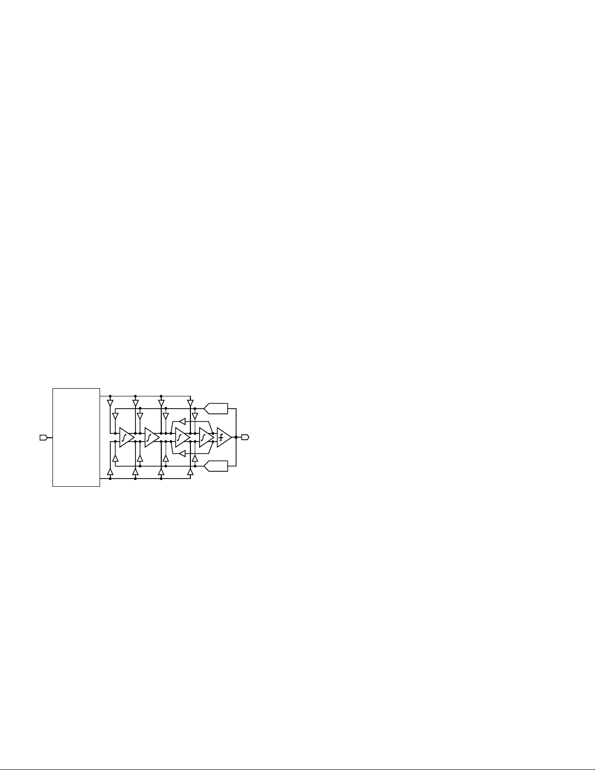
⌺⌬ Modulator Noise-Shaping
The stereo, internally differential analog modulator of the
AD1877 employs a proprietary feedforward and feedback architecture that passes input signals in the audio band with a unity
transfer function yet simultaneously shapes the quantization
noise generated by the one-bit comparator out of the audio
band. See Figure 1. Without the ∑∆ architecture, this quantization noise would be spread uniformly from dc to one-half the
oversampling frequency, 64 × F
V
IN
SINGLE TO
DIFFERENTIAL
CONVERTER
Figure 1. Modulator Noise-Shaper (One Channel)
∑∆ architectures “shape” the quantization noise-transfer function
in a nonuniform manner. Through careful design, this transfer
function can be specified to high-pass filter the quantization
noise out of the audio band into higher frequency regions. The
AD1877 also incorporates a feedback resonator from the fourth
integrator’s output to the third integrator’s input. This resonator
does not affect the signal transfer function but allows the flexible
placement of a zero in the noise transfer function for more effective noise shaping.
Oversampling by 64 simplifies the implementation of a high performance audio analog-to-digital conversion system. Antialias
requirements are minimal; a single pole of filtering will usually
suffice to eliminate inputs near F
A fourth-order architecture was chosen both to strongly shape
the noise out of the audio band and to help break up the idle
tones produced in all ∑∆ architectures. These architectures have
a tendency to generate periodic patterns with a constant dc input, a
response that looks like a tone in the frequency domain. These
idle tones have a direct frequency dependence on the input dc
ⴙV
)
ⴚV
2
S-compatible,
.
S
IN
DAC
MODULATOR
BITSTREAM
OUTPUT
DAC
IN
and its higher multiples.
S
offset and indirect dependence on temperature and time as it
affects dc offset. The AD1877 suppresses idle tones 20 dB or
better below the integrated noise floor.
The AD1877’s modulator was designed, simulated, and exhaustively tested to remain stable for any input within a wide tolerance
of its rated input range. The AD1877 is designed to internally
reset itself should it ever be overdriven, to prevent it from going
instable. It will reset itself within 5 µs at a 48 kHz sampling
frequency after being overdriven. Overdriving the inputs will
produce a waveform “clipped” to plus or minus full scale.
See TPCs 1 through 16 for illustrations of the AD1877’s
typical analog performance as measured by an Audio Precision
System One. Signal-to(distortion + noise) is shown under a
range of conditions. Note that there is a small variance between
the AD1877 analog performance specifications and some of the
performance plots. This is because the Audio Precision System
One measures THD and noise over a 20 Hz to 24 kHz bandwidth, while the analog performance is specified over a 20 Hz to
20 kHz bandwidth (i.e., the AD1877 performs slightly better
than the plots indicate). The power supply rejection (TPC 5)
graph illustrates the benefits of the AD1877’s internal differential architecture. The excellent channel separation shown in
TPC 6 is the result of careful chip design and layout.
Digital Filter Characteristics
The digital decimator accepts the modulator’s stereo bitstream
and simultaneously performs two operations on it. First, the
decimator low-pass filters the quantization noise that the modulator shaped to high frequencies and filters any other out-of
audio-band input signals. Second, it reduces the data rate to an
output word rate equal to F
. The high frequency bitstream is
S
decimated to stereo 16-bit words at 48 kHz (or other desired
). The out-of-band one-bit quantization noise and other high
F
S
frequency components of the bitstream are attenuated by at
least 90 dB.
The AD1877 decimator implements a symmetric Finite Impulse
Response (FIR) filter which possesses a linear phase response.
This filter achieves a narrow transition band (0.1 × F
), high
S
stopband attenuation (> 90 dB), and low passband ripple
(< 0.006 dB). The narrow transition band allows the unattenuated digitization of 20 kHz input signals with F
as low as
S
44.1 kHz. The stopband attenuation is sufficient to eliminate
modulator quantization noise from affecting the output. Low
passband ripple prevents the digital filter from coloring the
audio signal. See TPC 7 for the digital filter’s characteristics.
The output from the decimator is available as a single serial
output, multiplexed between left and right channels.
Note that the digital filter itself is operating at 64 × F
. As a
S
consequence, Nyquist images of the passband, transition band,
and stopband will be repeated in the frequency spectrum at
multiples of 64 × F
. Thus the digital filter will attenuate to
S
greater than 90 dB across the frequency spectrum except for a
window ± 0.55 × F
wide centered at multiples of 64 × FS. Any
S
input signals, clock noise, or digital noise in these frequency
windows will not be attenuated to the full 90 dB. If the high
frequency signals or noise appear within the passband images
within these windows, they will not be attenuated at all, and
therefore input antialias filtering should be applied.
–6–
REV. A

AD1877
Sample Delay
The sample delay or “group delay” of the AD1877 is dominated
by the processing time of the digital decimation filter. FIR filters convolve a vector representing time samples of the input
with an equal-sized vector of coefficients. After each convolution, the input vector is updated by adding a new sample at one
end of the “pipeline” and discarding the oldest input sample at
the other. For an FIR filter, the time at which a step input appears
at the output will be when that step input is half way through
the input sample vector pipeline. The input sample vector
is updated every 64 × F
. The equation which expresses the
S
group delay for the AD1877 is:
Group Delay (sec) = 36/F
(Hz)
S
For the most common sample rates this can be summarized as:
F
S
Group Delay
48 kHz 750 µs
44.1 kHz 816 µs
32 kHz 1125 µs
Due to the linear phase properties of FIR filters, the group
delay variation, or differences in group delay at different frequencies is essentially zero.
OPERATING FEATURES
Voltage Reference and External Filter Capacitors
The AD1877 includes a +2.25 V on-board reference that determines the AD1877’s input range. The left and right reference
pins (14 and 15) should be bypassed with a 0.1 µF ceramic chip
capacitor in parallel with a 4.7 µF tantalum as shown below in
Figure 3. Note that the chip capacitor should be closest to the
pin. The internal reference can be overpowered by applying an
external reference voltage at the V
REF
L (Pin 14) and V
REF
R
(Pin 15) pins, allowing multiple AD1877s to be calibrated to
the same gain. It is not possible to overpower the left and right
reference pins individually; the external reference voltage
should be applied to both Pin 14 and Pin 15. Note that the reference pins must still be bypassed as shown in Figure 3.
It is possible to bypass each reference pin (V
L and V
REF
REF
R)
with a capacitor larger than the suggested 4.7 µF, however it is
not recommended. A larger capacitor will have a longer chargeup time which may extend into the autocalibration period, yielding incorrect results.
The AD1877 requires four external filter capacitors on Pins 11,
12, 17 and 18. These capacitors are used to filter the single-to
differential converter outputs, and are too large for practical
integration onto the die. They should be 470 pF NPO ceramic
chip type capacitors as shown in Figure 3, placed as close to the
AD1877 package as possible.
Sample Clock
An external master clock supplied to CLKIN (Pin 28) drives
the AD1877 modulator, decimator, and digital interface. As
with any analog-to-digital conversion system, the sampling clock
must be low jitter to prevent conversion errors. If a crystal oscillator is used as the clock source, it should be bypassed with a
0.1 µF capacitor, as shown below in Figure 3.
For the AD1877, the input clock operates at either 256 × F
384 × F
as selected by the 384/256 pin. When 384/256 is HI,
S
S
or
the 384 mode is selected and when 384/256 is LO, the 256
mode is selected. In both cases, the clock is divided down to
obtain the 64 × F
put word rate itself will be at F
clock required for the modulator. The out-
S
. This relationship is illustrated
S
for popular sample rates below:
256 Mode 384 Mode Modulator Output Word
CLKIN CLKIN Sample Rate Rate
12.288 MHz 18.432 MHz 3.072 MHz 48 kHz
11.2896 MHz 16.9344 MHz 2.822 MHz 44.1 kHz
8.192 MHz 12.288 MHz 2.048 MHz 32 kHz
The AD1877 serial interface will support both master and slave
modes. Note that in slave mode it is required that the serial
interface clocks are externally derived from a common source.
In master mode, the serial interface clock outputs are internally
derived from CLKIN.
Reset, Autocalibration and Power Down
The active LO RESET pin (Pin 23) initializes the digital decimation filter and clears the output data buffer. While in the reset
state, all digital pins defined as outputs of the AD1877 are
driven to ground (except for BCLK, which is driven to the state
defined by RDEDGE (Pin 6)). Analog Devices recommends
resetting the AD1877 on initial power up so that the device is
properly calibrated. The reset signal must remain LO for the
minimum period specified in “Specifications” above. The reset
pulse is asynchronous with respect to the master clock, CLKIN.
If, however, multiple AD1877s are used in a system, and it is
desired that they leave the reset state at the same time, the
common reset pulse should be made synchronous to CLKIN
(i.e., RESET should be brought HI on a CLKIN falling edge).
Multiple AD1877s can be synchronized to each other by using
a single master clock and a single reset signal to initialize all
devices. On coming out of reset, all AD1877s will begin sampling at the same time. Note that in slave mode, the AD1877 is
inactive (and all outputs are static, including WCLK) until the
first rising edge of LRCK after the first falling edge of LRCK.
This initial low going then high going edge of LRCK can be used
to “skew” the sampling start-up time of one AD1877 relative to
other AD1877s in a system. In the Data Position Controlled by
WCLK Input mode, WCLK must be HI with LRCK HI, then
WCLK HI with LRCK LO, then WCLK HI with LRCK HI
before the AD1877 starts sampling.
The AD1877 achieves its specified performance without the
need for user trims or adjustments. This is accomplished
through the use of on-chip automatic offset calibration that
takes place immediately following reset. This procedure nulls
out any offsets in the single-to-differential converter, the analog
modulator and the decimation filter. Autocalibration completes
in approximately 8192 × (1/(F
) seconds, and need only be
LRCK
performed once at power-up in most applications. [In slave
mode, the 8192 cycles required for autocalibration do not start
until after the first rising edge of LRCK following the first falling edge of LRCK.] The autocalibration scheme assumes that
the inputs are ac coupled. DC coupled inputs will work with the
AD1877, but the autocalibration algorithm will yield an incorrect offset compensation.
REV. A
–7–

AD1877
The AD1877 also features a power-down mode. It is enabled by
the active LO RESET Pin 23 (i.e., the AD1877 is in powerdown
mode while RESET is held LO). The power savings are specified in the ‘’Specifications’’ section above. The converter is shut
down in the power-down state and will not perform conversions.
The AD1877 will be reset upon leaving the power-down state, and
autocalibration will commence after the RESET pin goes HI.
Power consumption can be further reduced by slowing down the
master clock input (at the expense of input passband width).
Note that a minimum clock frequency, F
, is specified for
CLKIN
the AD1877.
Tag Overrange Output
The AD1877 includes a TAG serial output (Pin 27) which is
provided to indicate status on the level of the input voltage. The
TAG output is at TTL compatible logic levels. A pair of unsigned
binary bits are output, synchronous with LRCK (MSB then
LSB), that indicate whether the current signal being converted
is: more than 1 dB under full scale; within 1 dB under full scale;
within 1 dB over full scale; or more than 1 dB over full scale.
The timing for the TAG output is shown in TPCs 7 through 16.
Note that the TAG bits are not “sticky,” i.e., they are not peak
reading, but rather change with every sample. Decoding of these
two bits is as follows:
TAG Bits
MSB, LSB Meaning
0 0 More Than 1 dB Under Full Scale
0 1 Within 1 dB Under Full Scale
1 0 Within 1 dB Over Full Scale
1 1 More Than 1 dB Over Full Scale
APPLICATIONS ISSUES
Recommended Input Structure
The AD1877 input structure is single-ended to allow the board
designer to achieve a high level of functional integration. The
very simple recommended input circuit is shown in Figure 2.
Note the 1 µF ac coupling capacitor which allows input level
shifting for 5 V only operation, and for autocalibration to
properly null offsets. The 3 dB point of the single-pole antialias
RC filter is 240 kHz, which results in essentially no attenuation
at 20 kHz. Attenuation at 3 MHz is approximately 22 dB, which
is adequate to suppress F
noise modulation. If the analog inputs
S
are externally ac coupled, then the 1 µF ac coupling capacitors
shown in Figure 2 are not required.
RIGHT
INPUT
LEFT
INPUT
300⍀
300⍀
2.2nF
NPO
2.2nF
NPO
1F
1F
19
10
VINR
AD1877
V
L
IN
Figure 2. Recommended Input Structure for Externally
DC Coupled Inputs
Analog Input Voltage Swing
The single-ended input range of the analog inputs is specified in
relative terms in the “Specifications” section of this data sheet.
The input level at which clipping occurs linearly tracks the voltage
reference level, i.e., if the reference is high relative to the typical
2.25 V, the allowable input range without clipping is correspondingly wider; if the reference is low relative to the typical
2.25 V, the allowable input range is correspondingly narrower.
Thus the maximum input voltage swing can be computed using
the following ratio:
22531.( )
V no al reference voltage
min
.
V p p no al voltage swing
min ma−
(
=
Y Volts ximum swing without clipping
)
()
X Volts measured reference voltage
()
Layout and Decoupling Considerations
Obtaining the best possible performance from the AD1877
requires close attention to board layout. Adhering to the following principles will produce typical values of 92 dB dynamic
range and 90 dB S/(THD+N) in target systems. Schematics and
layout artwork of the AD1877 Evaluation Board, which implement
these recommendations, are available from Analog Devices.
The principles and their rationales are listed below. The first
two pertain to bypassing and are illustrated in Figure 3.
470pF
NPO
4.7F
0.1F
470pF
NPO
13
AGNDL V
REFLVREF
CAPL2
12
CAPL1
11
AGND AVDDDVDD1 DGND1
20
0.1F
1F
5V
ANALOG5VDIGITAL
14
4.7F
0.1F
15 16
R
AGNDR
AD1877
4
10nF
1F
17
CAPR2 CAPR1
DGND2 DV
24
59
470pF
NPO
10nF
1F
18
CLKIN
DD
25
5V
DIGITAL
470pF
NPO
28
2
5V
DIGITAL
0.1F
OSCILLATOR
Figure 3. Recommended Bypassing and Oscillator Circuits
There are two pairs of digital supply pins on opposite sides of
the part (Pins 4 and 5 and Pins 24 and 25). The user should
tie a bypass chip capacitor (10 nF ceramic) in parallel with a
decoupling capacitor (1 µF tantalum) on EACH pair of supply
pins as close to the pins as possible. The traces between these
package pins and the capacitors should be as short and as wide
as possible. This will prevent digital supply current transients
from being inductively transmitted to the inputs of the part.
Use a 0.1 µF chip analog capacitor in parallel with a 1.0 µF
tantalum capacitor from the analog supply (Pin 9) to the analog
ground plane. The trace between this package pin and the
capacitor should be as short and as wide as possible.
The AD1877 should be placed on a split ground plane. The
digital ground plane should be placed under the top end of the
package, and the analog ground plane should be placed under
the bottom end of the package as shown in Figure 4. The split
should be between Pins 8 and 9 and between Pins 20 and 21.
–8–
REV. A

AD1877
The ground planes should be tied together at one spot underneath the center of the package with an approximately 3 mm
trace. This ground plane technique also minimizes RF transmission and reception.
LRCK
WCLK
BCLK
DV
DD
DGND1
RDEDGE
S/M
384/256
AV
VINL
CAPL1
CAPL2
AGNDL
V
REF
1
2
3
4
1
DD
L
DIGITAL GROUND PLANE
5
6
7
8
9
10
11
ANALOG GROUND PLANE
12
13
14
28
27
26
25
24
23
22
21
20
19
18
17
16
15
CLKIN
TAG
SOUT
DV
DD
DGND2
RESET
MSBDLY
RLJUST
AGND
R
V
IN
CAPR1
CAPR2
AGNDR
V
R
REF
2
drawn from the digital supply pins and help keep the IC substrate quiet.
How to Extend SNR
A cost-effective method of improving the dynamic range and
SNR of an analog-to-digital conversion system is to use multiple
AD1877 channels in parallel with a common analog input. This
technique makes use of the fact that the noise in independent
modulator channels is uncorrelated. Thus every doubling of the
number of AD1877 channels used will improve system dynamic
range by 3 dB. The digital outputs from the corresponding decimator channels have to be arithmetically averaged to obtain the
improved results in the correct data format. A microprocessor,
either general-purpose or DSP, can easily perform the averaging
operation.
Shown below in Figure 5 is a circuit for obtaining a 3 dB
improvement in dynamic range by using both channels of a
single AD1877 with a mono input. A stereo implementation
would require using two AD1877s and using the recommended
input structure shown in Figure 2. Note that a single microprocessor would likely be able to handle the averaging requirements
for both left and right channels.
SINGLE
CHANNEL
INPUT
AD1877
RECOMMENDED
INPUT BUFFER
VINR
AD1877
L
V
IN
DIGITAL
AVERAGER
SINGLE
CHANNEL
OUTPUT
Figure 4. Recommended Ground Plane
Each reference pin (14 and 15) should be bypassed with a 0.1 µF
ceramic chip capacitor in parallel with a 4.7 µF tantalum capaci-
tor. The 0.1 µF chip cap should be placed as close to the pack-
age pin as possible, and the trace to it from the reference pin
should be as short and as wide as possible. Keep this trace away
from any analog traces (Pins 10, 11, 12, 17, 18, 19)! Coupling
between input and reference traces will cause even order harmonic distortion. If the reference is needed somewhere else on
the printed circuit board, it should be shielded from any signal
dependent traces to prevent distortion.
Wherever possible, minimize the capacitive load on the digital
outputs of the part. This will reduce the digital spike currents
Figure 5. Increasing Dynamic Range By Using Two
AD1877 Channels
DIGITAL INTERFACE
Modes of Operation
The AD1877’s flexible serial output port produces data in
two’s-complement, MSB-first format. The input and output signals are TTL logic level compatible. Time multiplexed serial
data is output on SOUT (Pin 26), left channel then right channel, as determined by the left/right clock signal LRCK (Pin 1).
Note that there is no method for forcing the right channel to
precede the left channel. The port is configured by pin selections. The AD1877 can operate in either master or slave mode,
with the data in right-justified, I
2
S-compatible, Word Clock
controlled or left-justified positions.
The various mode options are pin-programmed with the Slave/
Master Pin (7), the Right/Left Justify Pin (21), and the MSB
Delay Pin (22). The function of these pins is summarized as
follows:
REV. A
–9–

AD1877
S/M RLJUST MSBDLY WCLK BCLK LRCK Serial Port Operation Mode
1 1 1 Output Input Input Slave Mode. WCLK frames the data. The MSB is output on the
17th BCLK cycle. Provides right-justified data in slave mode
with a 64 × FS BCLK frequency. See Figure 7.
1 1 0 Input Input Input Slave Mode. The MSB is output in the BCLK cycle after
WCLK is detected HI. WCLK is sampled on the BCLK active
edge, with the MSB valid on the next BCLK active edge. Tying
WCLK HI results in I2S-justified data. See Figure 8.
1 0 1 Output Input Input Slave Mode. Data left-justified with WCLK framing the data.
WCLK rises immediately after an LRCK transition. The MSB is
valid on the first BCLK active edge. See Figure 9.
2
1 0 0 Output Input Input Slave Mode. Data I
WCLK rises in the second BCLK cycle after an LRCK transition. The MSB is valid on the second BCLK active edge. See
Figure 10.
0 1 1 Output Output Output Master Mode. Data right-justified. WCLK frames the data,
going HI in the 17th BCLK cycle. BCLK frequency = 64 × FS.
See Figure 11.
0 1 0 Output Output Output Master Mode. Data right-justified + 1. WCLK is pulsed in the
17th BCLK cycle, staying HI for only 1 BCLK cycle. BCLK
frequency = 64 × FS. See Figure 12.
0 0 1 Output Output Output Master Mode. Data left-justified. WCLK frames the data.
BCLK frequency = 64 × FS. See Figure 13.
0 0 0 Output Output Output Master Mode. Data I
BCLK frequency = 64 × FS. See Figure 14.
S-justified with WCLK framing the data.
2
S-justified. WCLK frames the data.
Serial Port Data Timing Sequences
The RDEDGE input (Pin 6) selects the bit clock (BCLK) polarity.
RDEDGE HI causes data to be transmitted on the BCLK falling
edge and valid on the BCLK rising edge; RDEDGE LO causes
data to be transmitted on the BCLK rising edge and valid on
the BCLK falling edge. This is shown in the serial data output
timing diagrams. The term “sampling” is used generically to
denote the BCLK edge (rising or falling) on which the serial
data is valid. The term “transmitting” is used to denote the
other BCLK edge. The S/M input (Pin 7) selects slave mode (S/
M HI) or master mode (S/M LO). Note that in slave mode,
BCLK may be continuous or gated (i.e., a stream of pulses during the data phase followed by periods of inactivity between
channels).
In the master modes, the bit clock (BCLK), the left/right clock
(LRCK), and the word clock (WCLK) are always outputs, generated internally in the AD1877 from the master clock (CLKIN)
input. In master mode, a LRCK cycle defines a 64-bit “frame.”
LRCK is HI for a 32-bit “field” and LRCK is LO for a 32-bit
“field.”
In the slave modes, the bit clock (BCLK), and the left/right clock
(LRCK) are user-supplied inputs. The word clock (WCLK) is an
internally generated output except when S/M is HI, RLJUST is
HI, and MSBDLY is LO, when it is a user-supplied input which
controls the data position. Note that the AD1877 does not support asynchronous operation in slave mode; the clocks (CLKIN,
LRCK, BCLK and WCLK) must be externally derived from a
common source. In general, CLKIN should be divided down
externally to create LRCK, BCLK and WCLK.
In the slave modes, the relationship between LRCK and BCLK
is not fixed, to the extent that there can be an arbitrary number
of BCLK cycles between the end of the data transmission and
the next LRCK transition. The slave mode timing diagrams are
therefore simplified as they show precise 32-bit fields and 64-bit
frames.
In two slave modes, it is possible to pack two 16-bit samples in
a single 32-bit frame, as shown in Figures 15 and 16. BCLK,
LRCK, DATA and TAG operate at one half the frequency
(twice the period) as in the 64-bit frame modes. This 32-bit
frame mode is enabled by pulsing the LRCK HI for a minimum
of one BCLK period to a maximum of sixteen BCLK periods.
The LRCK HI for one BCLK period case is shown in Figures
15 and 16. With a one or two BCLK period HI pulse on
LRCK, note that both the left and right TAG bits are output
immediately, back-to-back. With a three to sixteen BCLK period
HI pulse on LRCK, the left TAG bits are followed by one to
fourteen “dead” cycles (i.e., zeros) followed by the right TAG
bits. Also note that WCLK stays HI continuously when the
AD1877 is in the 32-bit frame mode. Figure 15 illustrates the
left-justified case, while Figure 16 illustrates the I
2
S-justified case.
In all modes, the left and right channel data is updated with the
next sample within the last 1/8 of the current conversion cycle (i.e.,
within the last 4 BCLK cycles in 32-bit frame mode, and within
the last 8 BCLK cycles in 64-bit frame mode). The user must
constrain the output timing such that the MSB of the right channel
is read before the final 1/8 of the current conversion period.
–10–
REV. A

AD1877
Two modes deserve special discussion. The first special mode,
“Slave Mode, Data Position Controlled by WCLK Input” (S/M
= HI, RLJUST = HI, MSBDLY = LO), shown in Figure 8, is
the only mode in which WCLK is an input. The 16-bit output
data words can be placed at user-defined locations within 32-bit
fields. The MSB will appear in the BCLK period after WCLK is
detected HI by the BCLK sampling edge. If WCLK is HI during the first BCLK of the 32-bit field (if WCLK is tied HI for
example), then the MSB of the output word will be valid on the
sampling edge of the second BCLK. The effect is to delay the
MSB for one bit clock cycle into the field, making the output
data compatible at the data format level with the I
2
S data format. Note that the relative placement of the WCLK input can
vary from 32-bit field to 32-bit field, even within the same
64-bit frame. For example, within a single 64-bit frame, the left
word could be right justified (by pulsing WCLK HI on the 16th
BCLK) and the right word could be in an I
2
S-compatible data
format (by having WCLK HI at the beginning of the second field).
In the second special mode “Master Mode, Right-Justified with
MSB Delay, WCLK Pulsed in 17th Cycle” (S/M = LO,
RLJUST = HI, MSBDLY = LO), shown in Figure 12, WCLK
is an output and is pulsed for one cycle by the AD1877. The
MSB is valid on the 18th BCLK sampling edge, and the LSB
extends into the first BCLK period of the next 32-bit field.
Timing Parameters
For master modes, a BCLK transmitting edge (labeled “XMIT”)
will be delayed from a CLKIN rising edge by t
DLYCKB
, as shown
in Figure 17. A LRCK transition will be delayed from a BCLK
transmitting edge by t
delayed from a BCLK transmitting edge by t
. A WCLK rising edge will be
DLYBLR
DLYBWR
, and a WCLK
falling edge will be delayed from a BCLK transmitting edge by
t
transmitting edge of BCLK by t
. The DATA and TAG outputs will be delayed from a
DLYBWF
DLYDT
.
For slave modes, an LRCK transition must be setup to a BCLK
sampling edge (labeled “SAMPLE”) by t
SETLRBS.
The DATA
and TAG outputs will be delayed from an LRCK transition by
t
DLYLRDT
BCLK transmitting edge by t
, and DATA and TAG outputs will be delayed from
. For “Slave Mode, Data
DLYBDT
Position Controlled by WCLK Input,” WCLK must be setup to
a BCLK sampling edge by t
SETWBS
.
For both master and slave modes, BCLK must have a minimum
LO pulsewidth of t
, and a minimum HI pulsewidth of t
BPWL
BPWH
.
The AD1877 CLKIN and RESET timing is shown in Figure
19. CLKIN must have a minimum LO pulsewidth of t
a minimum HI pulse width of t
CLKIN is given by t
pulsewidth of t
RPWL
. RESET must have a minimum LO
CLKIN
. Note that there are no setup or hold time
. The minimum period of
CPWH
CPWL
, and
requirements for RESET.
Synchronizing Multiple AD1877s
Multiple AD1877s can be synchronized by making all the
AD1877s serial port slaves. This option is illustrated in
Figure 6. See the “Reset, Autocalibration and Power Down”
section above for additional information.
CLOCK
SOURCE
#1 AD1877
SLAVE MODE
RESET
CLKIN
#2 AD1877
SLAVE MODE
RESET
CLKIN
#N AD1877
SLAVE MODE
RESET
CLKIN
DATA
BCLK
WCLK
LRCK
DATA
BCLK
WCLK
LRCK
DATA
BCLK
WCLK
LRCK
Figure 6. Synchronizing Multiple AD1877s
REV. A
–11–

AD1877–Typical Performance Characteristic Curves
0
ⴚ20
ⴚ40
ⴚ60
ⴚ80
dBFS
ⴚ100
ⴚ120
ⴚ140
2022201816141210864
FREQUENCY – kHz
TPC 1. 1 kHz Tone at –0.5 dBFS (16k-Point FFT)
0
–20
–40
–60
–80
dBFS
–100
–120
ⴚ80
ⴚ82
ⴚ84
ⴚ86
ⴚ88
ⴚ90
dBFS
ⴚ92
ⴚ94
ⴚ96
ⴚ98
24
ⴚ100
2
0
AMPLITUDE – dBFS
20
1816141210864
TPC 4. THD+N versus Amplitude at 1 kHz
ⴚ60
ⴚ65
ⴚ70
ⴚ75
ⴚ80
dBFS
ⴚ85
ⴚ90
ⴚ95
–140
2
0
FREQUENCY – kHz
22201816141210864
TPC 2. 1 kHz Tone at –10 dBFS (16k-Point FFT)
ⴚ80
ⴚ82
ⴚ84
ⴚ86
ⴚ88
ⴚ90
dBFS
ⴚ92
ⴚ94
ⴚ96
ⴚ98
ⴚ100
2
0
FREQUENCY – kHz
1816141210864
TPC 3. THD+N versus Frequency at –0.5 dBFS
24
ⴚ100
20
AMPLITUDE – kHz
TPC 5. Power Supply Rejection to 300 mV p-p on AV
ⴚ80
ⴚ85
ⴚ90
ⴚ95
ⴚ100
dBFS
ⴚ105
ⴚ110
ⴚ115
20
ⴚ120
2
0
FREQUENCY – kHz
20
1816141210864
DD
20
1816141210864
TPC 6. Channel Separation versus Frequency at –0.5 dBFS
REV. A–12–

–10
–20
–30
–40
–50
–60
dBFS
–70
–80
–90
–100
–110
AD1877
0
LRCK
INPUT
BCLK
RDEDGE = LO
INPUT
BCLK
RDEDGE = HI
SOUT
OUTPUT
WCLK
OUTPUT
TAG
OUTPUT
LRCK
INPUT
BCLK
RDEDGE= LO
INPUT
BCLK
RDEDGE = HI
SOUT
OUTPUT
WCLK
INPUT
TAG
OUTPUT
0.10.0
NORMALIZED F
S
TPC 7. Digital Filter Signal Transfer Function to F
31 32 1 2 15 16 17 18 19 32 1 2 15 16 17 18 19 32 1 2
PREVIOUS DATA
MSB-14 LSB
ZEROS
LEFT TAG
MSB LSB
LEFT DATA
MSB MSB
MSB-1
MSB-2
LSB
ZEROS
RIGHT TAG
MSB LSB
1.0
0.90.80.70.60.50.40.30.2
S
RIGHT DATA
MSB-1 MSB-2
LSB
Figure 7. Serial Data Output Timing: Slave Mode, Right-Justified with No MSB Delay,
S/M = Hl, RLJUST = Hl, MSBDLY = Hl
1234 17 1234 17
MSB
RIGHT DATA
MSB
LSB
MSB-1 MSB-2
LSB
ZEROS
LEFT TAG
MSB
MSB
LSB
LEFT DATA
MSB-1
MSB-2
LSB
ZEROS
RIGHT TAG
ZEROS
LEFT TAG
MSB LSB
ZEROS
S/
REV. A
Figure 8. Serial Data Output Timing: Slave Mode, Data Position Controlled by WCLK Input,
M
= Hl, RLJUST= Hl,
MSBDLY
= LO
–13–

AD1877
RDEDGE = LO
RDEDGE = HI
RDEDGE = LO
RDEDGE = HI
LRCK
INPUT
BCLK
INPUT
BCLK
SOUT
OUTPUT
WCLK
OUTPUT
TAG
OUTPUT
LRCK
INPUT
BCLK
INPUT
BCLK
SOUT
OUTPUT
WCLK
OUTPUT
TAG
OUTPUT
31 32 1 2 3 4 16
MSB
MSB
LEFT DATA
MSB-1
LEFT TAG
LSB
MSB-2
LSB
17 18 17 18
31 32 1 2 3 4 16
ZEROSZEROS
RIGHT DATA
MSB
MSB
MSB-1
RIGHT TAG
LSB
MSB-2
LSB
ZEROS
Figure 9. Serial Data Output Timing: Slave Mode, Left-Justified with No MSB Delay, S/M = Hl,
R
L
JUST = LO,
32 1 2 3 4 17
ZEROS
LEFT TAG
MSB
MSB
LSB
LEFT DATA
MSBDLY
MSB-1
MSB-2
= Hl
5 5
LSB
31 32 1 2 3 4 17
MSB
RIGHT DATA
MSB
LSB
MSB-1
MSB-2
ZEROS
RIGHT TAG
LSB
ZEROS
Figure 10. Serial Data Output Timing: Slave Mode, I2S-Justified, S/M = Hl, RLJUST = LO,
LRCK
OUTPUT
BCLK
RDEDGE = LO
OUTPUT
BCLK
RDEDGE = HI
SOUT
OUTPUT
WCLK
OUTPUT
OUTPUT
31 32 1 2 15 16 17 18 19 32 1 2 15 16 17 18 19 32 1 2
PREVIOUS DATA
MSB-14 LSB
TAG
ZEROS ZEROS
LEFT TAG
MSB LSB
LEFT DATA
MSB MSB
MSB-1
MSB-2
LSB
RIGHT TAG
MSB LSB
RIGHT DATA
MSB-1 MSB-2
Figure 11. Serial Data Output Timing: Master Mode, Right-Justified with No MSB Delay, S/M = LO,
L
JUST = Hl,
R
MSBDLY
= Hl
MSBDLY
LSB
= LO
ZEROS
LEFT TAG
MSB LSB
–14–
REV. A

LRCK
OUTPUT
BCLK
RDEDGE = LO
OUTPUT
BCLK
RDEDGE = HI
SOUT
OUTPUT
WCLK
OUTPUT
OUTPUT
32 1 2 16 17 18 19 1 2 16 17 18 19 20 1 2
PREVIOUS DATA
MSB-14 LSB
TAG
LEFT TAG
MSB LSB
ZEROS ZEROS
LEFT DATA
MSB MSB
MSB-1
Figure 12. Serial Data Output Timing. Master Mode, Right-Justified with MSB Delay,
WCLK Pulsed in 17th BCLK Cycle, S/
LRCK
OUTPUT
BCLK
RDEDGE = LO
OUTPUT 17 1817 18
BCLK
RDEDGE = HI
SOUT
OUTPUT
WCLK
OUTPUT
TAG
OUTPUT
31 32 1 2 3 16
MSB
MSB
LEFT DATA
MSB-1
LEFT TAG
LSB
MSB-2
LSB
20
MSB-2
M
= LO, RLJUST = Hl,
LSB
RIGHT TAG
MSB LSB
ZEROSZEROS ZEROS
RIGHT DATA
MSB-1 MSB-2
MSBDLY
31 32 1 2 3 16
RIGHT DATA
MSB
RIGHT TAG
MSB
= LO
MSB-1
LSB
MSB-2
LSB
AD1877
ZEROS
LSB
LRCK
OUTPUT
BCLK
RDEDGE = LO
OUTPUT
BCLK
RDEDGE = HI
SOUT
OUTPUT
WCLK
OUTPUT
TAG
OUTPUT
Figure 13. Serial Data Output Timing: Master Mode, Left-Justified with No MSB Delay,
S/
M
= LO, RLJUST = LO,
321234 17
LEFT DATA
MSB
MSB-1
LEFT TAG
MSB
LSB
MSB-2
MSBDLY
LSB
= Hl
31 32 1 2 3 4 17
MSB
RIGHT DATA
MSB
LSB
MSB-1
MSB-2
LSB
ZEROSZEROS ZEROS
RIGHT TAG
Figure 14. Serial Data Output Timing: Master Mode, I2S-Justified, S/M = LO, RLJUST = LO,
MSBDLY
= LO
REV. A
–15–

AD1877
LRCK
INPUT
BCLK
RDEDGE = LO
INPUT
BCLK
RDEDGE = HI
SOUT
OUTPUT
WCLK
OUTPUT
TAG
OUTPUT
31 32 1 2 3 4 16
PREVIOUS DATA
LSB
MSB-14
LEFT DATA
MSB
MSB-1 MSB-2 MSB-3
LEFT TAG
LSB
MSB
RIGHT TAG LEFT TAG
MSB LSB
51718
MSB-4 MSB-3 MSB-4
HI HI
19 20 21 32 1 2
LSB
RIGHT DATA
MSB MSB
MSB-1 MSB-2
Figure 15. Serial Data Output Timing: Slave Mode, Left-Justified with No MSB Delay,
M
32-Bit Frame Mode, S/
LRCK
INPUT
BCLK
RDEDGE = LO
INPUT
BCLK
RDEDGE = HI
SOUT
OUTPUT
WCLK
OUTPUT
TAG
OUTPUT
32 1 2 3 4 5 17
PREVIOUS DATA
MSB-14
LSB
LEFT TAG
MSB
LEFT DATA
MSB
MSB-1 MSB-2 MSB-3
RIGHT TAG
MSB LSB
LSB
= Hl, RLJUST = LO,
61819
MSB-4 MSB-3 MSB-4
HI HI
MSBDLY
LSB
= Hl
20 21 22 1 2 3
RIGHT DATA
MSB MSB
MSB-1 MSB-2
LSB
LSB
LEFT TAG
MSB
LEFT DATA
MSB
LEFT DATA
LSB
MSB-1
LSB
MSB-1
RIGHT TAG
MSB
Figure 16. Serial Data Output Timing: Slave Mode, I2S-Justified, 32-Bit Frame Mode,
S/
M
= Hl, RLJUST= LO,
CLKIN
INPUT
BCLK OUTPUT (64 x FS)
RDEDGE = LO
BCLK OUTPUT (64 x FS)
RDEDGE = HI
LRCK
OUTPUT
WCLK
OUTPUT
DATA & TAG
OUTPUTS
MSBDLY
t
DLYCKB
XMIT XMITXMIT XMIT
t
DLYBLR
= LO
t
DLYBWR
t
DLYBWF
Figure 17. Master Mode Clock Timing
t
DLYDT
t
BPWL
t
BPWH
t
BPWH
t
BPWL
–16–
REV. A

AD1877
CLKIN INPUT
RESET INPUT
BCLK INPUT
RDEDGE = LO
BCLK OUTPUT
RDEDGE = HI
LRCK
INPUT
WCLK
INPUT
DATA & TAG
OUTPUTS
t
CPWH
XMIT SAMPLE SAMPLE
t
SETLRBS
t
SETWBS
t
DLYLRDT
XMIT
t
MSB MSB-1
DLYBDT
Figure 18. Slave Mode Clock Timing
t
CLKIN
t
CPWL
t
RPWL
Figure 19. CLKIN and
RESET
t
BPWL
t
BPWH
Timing
t
BPWH
t
BPWL
REV. A
–17–

AD1877
OUTLINE DIMENSIONS
Dimensions shown in inches and (mm).
28-Lead Wide-Body SO
28 15
PIN 1
1
R-28 (S-Suffix)
SOL-28
0.2992 (7.60)
0.2914 (7.40)
14
0.4193 (10.65)
0.3937 (10.00)
0.0118 (0.30)
0.0040 (0.10)
0.7125 (18.10)
0.6969 (17.70)
0.0500 (1.27)
BSC
0.0192 (0.49)
0.0138 (0.35)
0.1043 (2.65)
0.0926 (2.35)
0.0125 (0.32)
0.0091 (0.23)
8
ⴗ
0
ⴗ
0.0291 (0.74)
0.0098 (0.25)
0.0500 (1.27)
0.0157 (0.40)
x 45
°
–18–
REV. A

–19–

C00749–0–8/00 (rev. A)
–20–
PRINTED IN U.S.A.
 Loading...