

Page 1
Parallel-Port 16-Bit
a
FEATURES
Single-Chip Integrated ∑∆ Digital Audio Stereo Codec
Microsoft® and Windows® Sound System Compatible
MPC Level-2+ Compliant Mixing
16 mA Bus Drive Capability
Supports Two DMA Channels for Full Duplex Operation
On-Chip Capture and Playback FIFOs
Advanced Power-Down Modes
Programmable Gain and Attenuation
Sample Rates from 4.0 kHz to 50 kHz Derived from a
Single Clock or Crystal Input
68-Lead PLCC, 100-Lead TQFP Packages
Operation from +5 V Supplies
Byte-Wide Parallel Interface to ISA and EISA Buses
Pin Compatible with AD1848, AD1846, CS4248, CS4231
PRODUCT OVERVIEW
The Parallel Port AD1845 SoundPort Stereo Codec integrates
key audio data conversion and control functions into a single
integrated circuit. The AD1845 provides a complete, single chip
computer audio solution for business audio and multimedia
applications. The codec includes stereo audio converters, com-
SoundPort® Stereo Codec
AD1845
plete on-chip filtering, MPC Level-2 compliant analog mixing,
programmable gain, attenuation and mute, a variable sample
frequency generator, FIFOs, and supports advanced powerdown modes. It provides a direct, byte-wide interface to both
ISA (“AT”) and EISA computer buses for simplified implementation on a computer motherboard or add-in card.
The AD1845 SoundPort Stereo Codec supports a DMA request/grant architecture for transferring data with the host computer bus. One or two DMA channels can be supported.
Programmed I/O (PIO) mode is also supported for control
register accesses and for applications lacking DMA control.
Two input control lines support mixed direct and indirect addressing of thirty-seven internal control registers over this asynchronous interface. The AD1845 includes dual DMA count
registers for full duplex operation enabling the AD1845 to capture data on one DMA channel and play back data on a separate
channel. The FIFOs on the AD1845 reduce the risk of losing
data when making DMA transfers over the ISA/EISA bus. The
FIFOs buffer data transfers and allow for relaxed timing in
acknowledging requests for capture and playback data.
(Continued on Page 9)
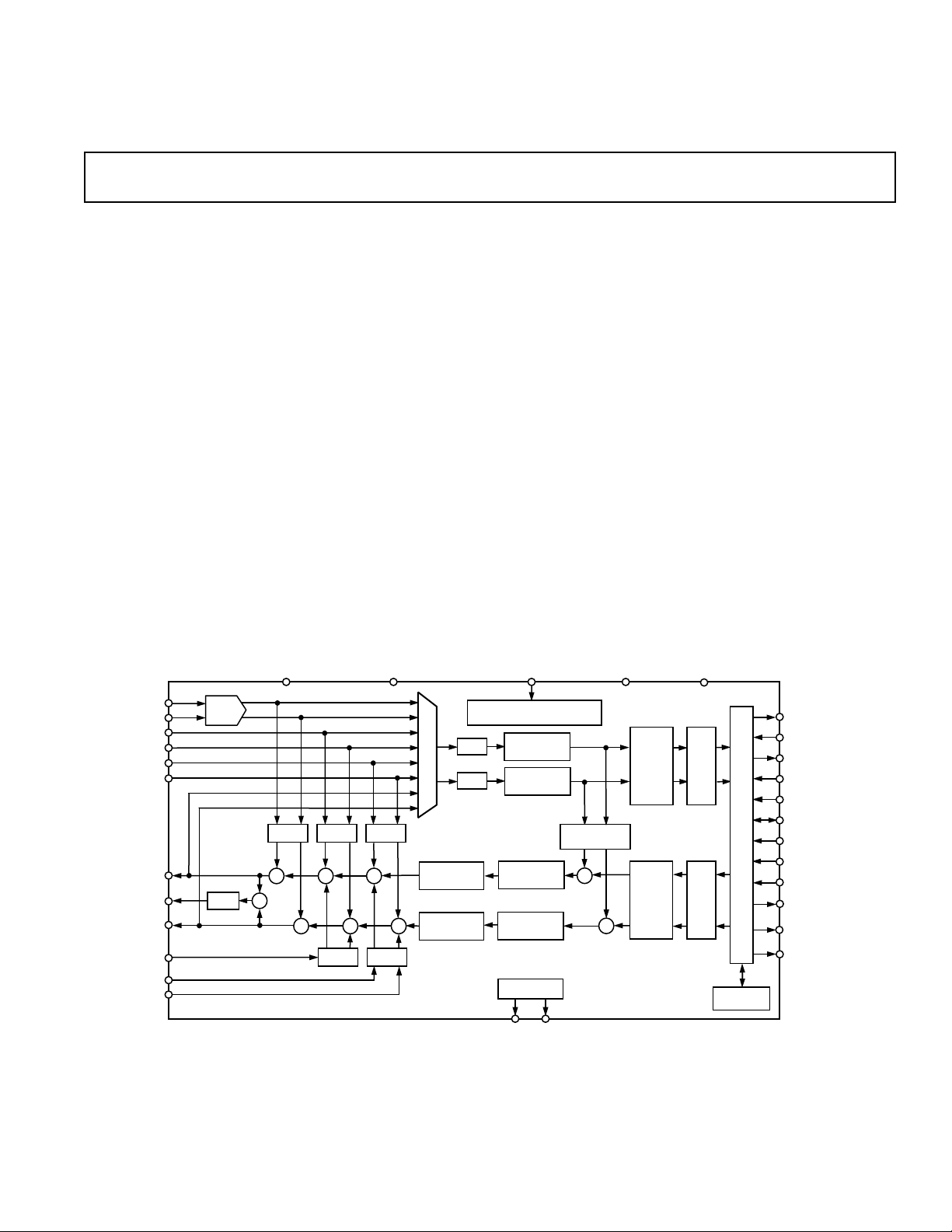
FUNCTIONAL BLOCK DIAGRAM
ANALOG
L_MIC
R_MIC
L_LINE
R_LINE
L_AUX1
R_AUX1
L_OUT
M_OUT
R_OUT
M_IN
L_AUX2
R_AUX2
SoundPort is a registered trademark of Analog Devices, Inc.
Microsoft and Windows are registered trademarks of Microsoft Corporation.
0 dB/
20 dB
MUTE
ANALOG SUPPLY
GAM
S
S
S S S
DIGITAL SUPPLY CLOCK SOURCE
L
M
GAIN
U
X
R
GAIN
GAM GAM
S S
GAM GAM
GAM = GAIN
ATTENTUATE
MUTE
L
ATTENUATE
MUTE
R
ATTENUATE
MUTE
VARIABLE SAMPLE
FREQUENCY GENERATOR
SD A/D
CONVERTER
SD A/D
CONVERTER
DIGITAL MIX
ATTENUATE
SD D/A
CONVERTER
SD D/A
CONVERTER
REFERENCE
V
REF_F
S
V
REF
POWER DOWN RESET
AD1845
m-LAW
A-LAW
LINEAR
m-LAW
A-LAW
LINEAR
S
FIFO
FIFO
P
A
R
A
L
L
E
L
P
O
R
T
CONTROL
REGISTERS
DIGITAL
PLAYBACK REQ
PLAYBACK ACK
CAPTURE REQ
CAPTURE ACK
ADR1:0
DATA7:0
CS
RD
WR
BUS DRIVER
CONTROL
HOST DMA
INTERRUPT
EXTERNAL
CONTROL
REV. C
Information furnished by Analog Devices is believed to be accurate and
reliable. However, no responsibility is assumed by Analog Devices for its
use, nor for any infringements of patents or other rights of third parties
which may result from its use. No license is granted by implication or
otherwise under any patent or patent rights of Analog Devices.
One Technology Way, P.O. Box 9106, Norwood, MA 02062-9106, U.S.A
Tel: 781/329-4700 World Wide Web Site: http://www.analog.com
Fax: 781/326-8703 © Analog Devices, Inc., 1997
Page 2

AD1845–SPECIFICA TIONS
STANDARD TEST CONDITIONS UNLESS OTHERWISE NOTED
Temperature 25 °C
Digital Supply (V
Analog Supply (V
Word Rate (F
) 5.0 V
DD
) 5.0 V
CC
) 48 kHz
S
Input Signal 1008 Hz
Analog Output Passband 20 Hz to 20 kHz
ADC FFT Size 2048
DAC FFT Size 8192
V
IH
V
IL
ANALOG INPUT
5V
0V
Input Voltage (RMS Values Assume Sine Wave Input)
Line 1 V rms
MIC with +20 dB Gain (MGE = 1) 0.1 V rms
MIC with 0 dB Gain (MGE = 0) 1 V rms
Input Impedance* 10 17 kΩ
Input Capacitance 15 pF
DAC Test Conditions
Calibrated
0 dB Relative to Full Scale
16-Bit Linear Mode
10 kΩ Output Load
Mute Off, OL = 0
ADC Test Conditions
Calibrated
0 dB Gain
–1.0 dB Relative to Full Scale
Line Input
16-Bit Linear Mode
Min Typ Max Units
2.55 2.83 3.35 V p-p
0.255 0.283 0.335 V p-p
2.55 2.83 3.35 V p-p
PROGRAMMABLE GAIN AMPLIFIER–ADC
Min Typ Max Units
Step Size (All Steps Tested)
(0 dB to 22.5 dB) 0.7 1.5 1.9 dB
PGA Gain Range Span 21.5 22.5 23.5 dB
AUXILIARY LINE, MONO, AND MICROPHONE INPUT ANALOG GAIN/AMPLIFIERS/ATTENUATORS
Min Typ Max Units
Step Size : AUX1, AUX2, LINE, MIC (All Steps Tested)
(+12 dB to –30 dB) 1.25 1.5 1.75 dB
(–31.5 dB to –34.5 dB) 1 1.5 2.0 dB
Step Size: M_IN (All Steps Tested)
(0 dB to –39 dB) 2.5 3.0 3.6 dB
(–42 dB to –45 dB) 2.2 3.0 3.85 dB
Input Gain/Attenuation Range: AUX1, AUX2, LINE, MIC 45.0 46.5 49.0 dB
Input Gain/Attenuation Range: M_IN 42 45 49 dB
DIGITAL DECIMATION AND INTERPOLATION FILTERS*
Min Max Units
Passband 0 0.4 × F
S
Hz
Passband Ripple ±0.1 dB
Transition Band 0.4 × F
Stopband 0.6 × F
S
S
0.6 × F
S
Hz
∞ Hz
Stopband Rejection 74 dB
Group Delay 15/F
S
Group Delay Variation Over Passband 0.0 µs
*Guaranteed, not tested.
–2–
REV. C
Page 3

AD1845
ANALOG-TO-DIGITAL CONVERTERS
Min Typ Max Units
Resolution 16 Bits
Dynamic Range (–60 dB Input, THD+N Referenced to Full Scale, A-Weighted) 73 81 dB
THD+N (Referenced to Full Scale) 0.025 %
–76 –72 dB
Signal-to-Intermodulation Distortion 85 dB
ADC Crosstalk*
Line Inputs (Input L, Ground R, Read R; Input R, Ground L, Read L) –90 –80 dB
Line to MIC (Input LINE, Ground and Select MIC, Read ADC) –90 –80 dB
Line to AUX1 –90 –80 dB
Line to AUX2 –90 –80 dB
Gain Error (Full-Scale Span Relative to Nominal Input Voltage) –18.5 +10 %
Interchannel Gain Mismatch (Difference of Gain Errors) ±0.9 dB
ADC Offset Error 10 mV
DIGITAL-TO-ANALOG CONVERTERS
Min Typ Max Units
Resolution 16 Bits
Dynamic Range (–60 dB Input, THD+N Referenced to Full Scale, A-Weighted) 74 82 dB
THD+N (Referenced to Full Scale) 0.032 %
–78 –70 dB
Signal-to-Intermodulation Distortion 90 dB
Gain Error (Full-Scale Span Relative to Nominal Output Voltage) –14.5 +10 %
Interchannel Gain Mismatch (Difference of Gain Errors) ±0.6 dB
DAC Crosstalk* (Input L, Zero R, Measure R_OUT; Input R, Zero L, Measure L_OUT) –80 dB
Total Out-of-Band Energy (Measured from 0.6 × F
Audible Out-of-Band Energy (Measured from 0.6 × FS to 20 kHz)* –70 dB
to 100 kHz)* –50 dB
S
DAC ATTENUATOR
Min Typ Max Units
Step Size (0 dB to –22.5 dB) 1.3 1.5 1.7 dB
Step Size (–22.5 dB to –94.5 dB)* 1.0 1.5 2.0 dB
Output Attenuation Range Span* 93.5 94.5 95.5 dB
ANALOG OUTPUT
Min Typ Max Units
Full-Scale Output Voltage
OL = 0 1.7 2.0 2.2 V p-p
OL = 1 2.4 2.83 3.11 V p-p
Output Impedance* 600 Ω
External Load Impedance 10 kΩ
Output Capacitance* 15 pF
External Load Capacitance 100 pF
V
REF
V
Current Drive 100 µA
REF
V
Output Impedance 4kΩ
REF
2.05 2.25 2.60 V
Mute Attenuation of 0 dB Fundamental* (L_OUT, R_OUT, M_OUT) –80 dB
Mute Click (Muted Output Minus Unmuted Midscale DAC Output)* ±5mV
*Guaranteed, not tested.
REV. C
–3–
Page 4

AD1845
SYSTEM SPECIFICATIONS
Min Typ Max Units
System Frequency Response Ripple (Line In to Line Out)* 1.0 dB
Differential Nonlinearity* ± 1 LSB
Phase Linearity Deviation* 5 Degrees
STATIC DIGITAL SPECIFICATIONS
Min Max Units
High Level Input Voltage (V
Digital Inputs 2.4 V
XTAL1I 2.4 V
Low Level Input Voltage (V
High Level Output Voltage (V
Low Level Output Voltage (V
Input Leakage Current –10 10 µA
Output Leakage Current –10 10 µA
TIMING PARAMETERS (GUARANTEED OVER OPERATING TEMPERATURE RANGE, VDD = VCC = 5.0 V)
WR/RD Strobe Width (t
WR/RD Rising to WR/RD Falling (t
Write Data Setup to
WR Rising (t
RD Falling to Valid Read Data (t
CS Setup to WR/RD Falling (t
CS Hold from WR/RD Rising (t
Adr Setup to
Adr Hold from
WR/RD Falling (t
WR/RD Rising (t
DAK Rising to WR/RD Falling (t
DAK Falling to WR/RD Rising (t
DAK Setup to WR/RD Falling (t
Data Hold from
Data Hold from
DRQ Hold from
RD Rising (t
WR Rising (t
WR/RD Falling (t
DAK Hold from WR Rising (t
DAK Hold from RD Rising (t
DBEN/DBDIR Delay from WR/RD Falling (t
PWRDWN and RESET Low Pulsewidth 300 ns
*Guaranteed, not tested.
)
IH
) 0.8 V
IL
) IOH = –2 mA 2.4 V
OH
) IOL = 2 mA 0.4 V
OL
Min Max Units
) 100 ns
STW
)80ns
BWND
)10ns
WDSU
)40ns
RDDV
)10ns
CSSU
)0ns
CSHD
)10ns
ADSU
)10ns
ADHD
)20ns
SUDK1
)0ns
SUDK2
)10ns
DKSU
)20ns
DHD1
)15ns
DHD2
)25ns
DRHD
)10ns
DKHDa
) 10 ns
DKHDb
) 30 ns
DBDL
–4–
REV. C
Page 5

AD1845
WARNING!
ESD SENSITIVE DEVICE
POWER SUPPLY
Min Typ Max Units
Power Supply Range–Digital and Analog 4.75 5.25 V
Power Supply Current 130 mA
Analog Supply Current 45 mA
Digital Supply Current 85 mA
Power Dissipation
(Current × Nominal Supplies) 650 mW
Power-Down Supply Current 2mA
Reset Supply Current 2mA
Total Power-Down Supply Current 30 mA
Standby Supply Current 36 mA
Mixer Power-Down Supply Current 70 mA
Mixer Only Supply Current 52 mA
ADC Power-Down Supply Current 80 mA
DAC Power-Down Supply Current 85 mA
Power Supply Rejection (100 mV p-p Signal @ 1 kHz)*
(At Both Analog and Digital Supply Pins, both ADCs and DACs) 40 dB
CLOCK SPECIFICATIONS*
Min Max Units
Input Clock Frequency 33 MHz
Recommended Clock Duty Cycle 10 90 %
Power Up Initialization Time 512 ms
*Guaranteed, not tested.
Specifications subject to change without notice.
ORDERING GUIDE
Temperature Package Package
Model Range Description Option
AD1845JP 0°C to +70°C 68-Lead PLCC P-68A
AD1845JP-REEL
AD1845JST 0°C to +70°C 100-Lead TQFP ST-100
NOTES
1
P = Plastic Leaded Chip Carrier; ST = Thin Quad Flatpack.
2
13" Reel, multiples of 250 pcs.
2
0°C to +70°C 68-Lead PLCC P-68A
ABSOLUTE MAXIMUM RATINGS*
1
Power Supplies
Digital (V
Analog (V
) –0.3 6.0 V
DD
) –0.3 6.0 V
CC
Input Current
(Except Supply Pins) ±10.0 mA
Analog Input Voltage (Signal Pins) –0.3 V
Digital Input Voltage (Signal Pins) –0.3 V
Ambient Temperature (Operating) 0 +70 °C
ENVIRONMENTAL CONDITIONS
Ambient Temperature Rating:
T
= T
AMB
T
= Case Temperature in °C
CASE
– (PD × θCA)
CASE
PD = Power Dissipation in W
θ
= Thermal Resistance (Case-to-Ambient)
CA
θ
= Thermal Resistance (Junction-to-Ambient)
JA
θ
= Thermal Resistance (Junction-to-Case)
JC
Package u
JA
u
JC
u
CA
Storage Temperature –65 +150 °C
*Stresses greater than those listed under Absolute Maximum Ratings may cause
permanent damage to the device. This is a stress rating only; functional operation
of the device at these or any other conditions above those indicated in the
operational section of this specification is not implied. Exposure to absolute
maximum rating conditions for extended periods may affect device reliability.
PLCC 38°C/W 8°C/W 30°C/W
TQFP 44°C/W 8 °C/W 93°C/W
CAUTION
ESD (electrostatic discharge) sensitive device. Electrostatic charges as high as 4000 V readily
accumulate on the human body and test equipment and can discharge without detection.
Although the AD1845 features proprietary ESD protection circuitry, permanent damage may
occur on devices subjected to high energy electrostatic discharges. Therefore, proper ESD
precautions are recommended to avoid performance degradation or loss of functionality.
Min Max Units
+0.3 V
CC
+0.3 V
DD
REV. C
–5–
Page 6
AD1845
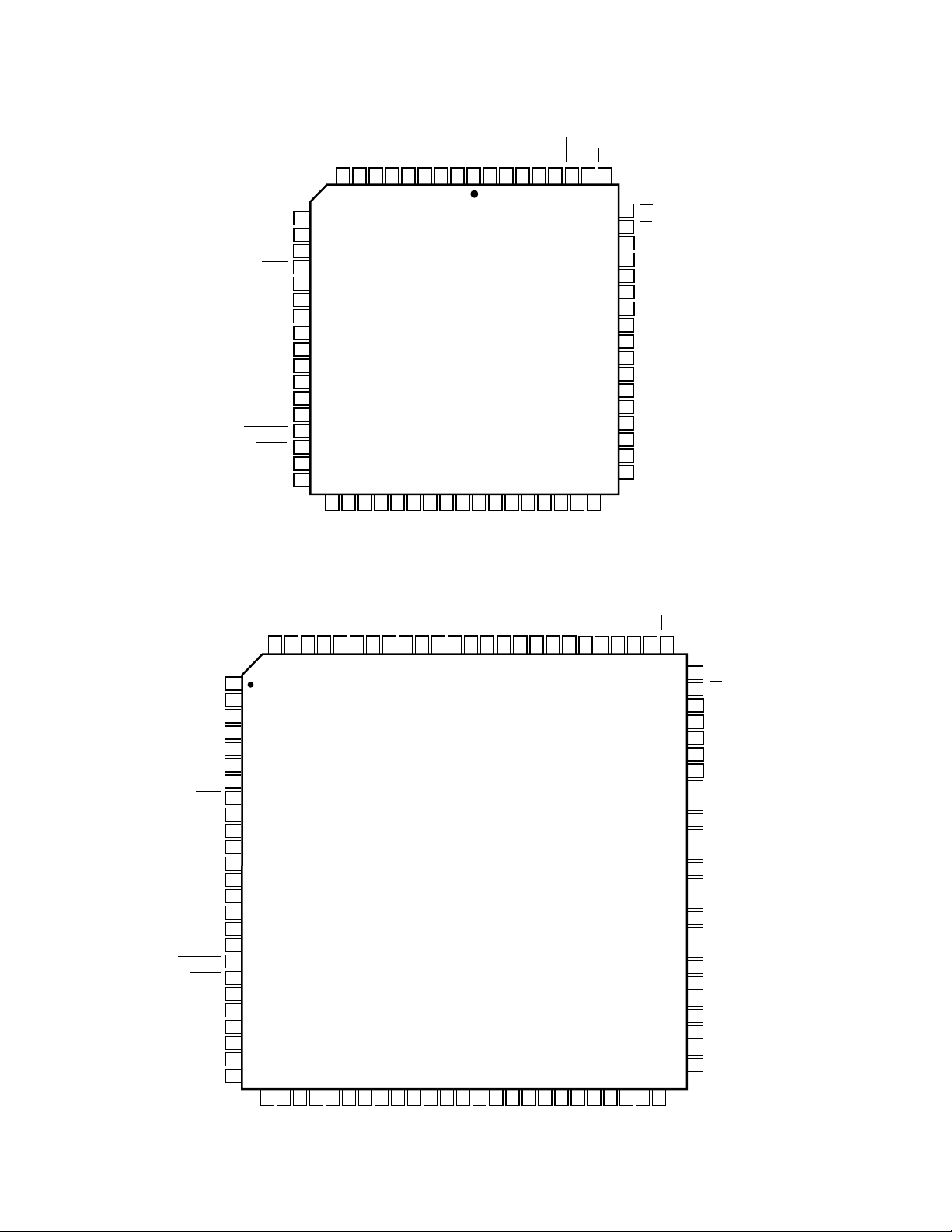
68-Lead PLCC
ADR0
CDAK
CDRQ
PDAK
PDRQ
V
GNDD
XTAL1I
XTAL1O
V
GNDD
XTAL2I
XTAL2O
PWRDWN
RESET
GNDD
R_FILT
PIN DESIGNATIONS
ADR1
GNDD
VDDDATA0
DATA1
DATA2
DATA3
GNDD
VDDDATA4
DATA5
DATA6
DATA7
GNDD
DBEN
DBDIR
R_OUT
R_AUX1
R_AUX2
WR
61
60
RD
59
CS
58
XCTL1
57
INT
56
XCTL0
55
NC
54
V
DD
53
GNDD
52
NC
51
NC
50
NC
49
NC
48
NC
47
M_OUT
46
M_IN
45
V
DD
44
GNDD
NC = NO CONNECT
987654321
10
11
12
13
14
15
DD
16
17
18
19
DD
20
21
22
23
24
25
26
2728293031323334353637383940414243
L_MIC
R_MIC
R_LINE
L_LINE
REF
V
L_FILT
AD1845
TOP VIEW
(Not to Scale)
REF_F
V
68676665646362
CC
VCCV
GNDA
GNDA
L_AUX2
L_AUX1
L_OUT
100-Lead TQFP
ADR0
NC
NC
NC
NC
CDAK
CDRQ
PDAK
PDRQ
V
GNDD
XTAL1I
XTAL1O
V
GNDD
XTAL2I
XTAL2O
PWRDWN
RESET
GNDD
NC
NC
NC
NC
R_FILT
ADR1
GNDD
VDDNCNCNCNCDATA0
9998979695949392919089888786858483828180797877
100
1
2
3
4
5
6
7
8
9
10
DD
11
12
13
14
DD
15
16
17
18
19
20
21
22
23
24
25
26272829303132333435363738394041424344454647484950
NC
NC
R_MIC
R_LINE
L_MIC
L_LINE
NC
NC
L_FILT
DATA1
DATA2
REF
V
DATA3
GNDD
VDDDATA4
AD1845
TOP VIEW
(Not to Scale)
NC
NC
REF_F
V
NC
DATA5
GNDA
DATA6
CCVCC
V
DATA7NCNCNCNC
GNDA
L_AUX2
L_AUX1
L_OUT
GNDD
R_OUT
R_AUX1
DBEN
DBDIR
WR
76
NC
R_AUX2
NC = NO CONNECT
RD
75
CS
74
XCTL1
73
INT
72
XCTL0
71
NC
70
NC
69
V
68
DD
GNDD
67
NC
66
NC
65
NC
64
NC
63
NC
62
NC
61
NC
60
NC
59
NC
58
M_OUT
57
M_IN
56
V
55
DD
54
GNDD
53
NC
52
NC
51
NC
–6–
REV. C
Page 7

AD1845
PIN FUNCTION DESCRIPTIONS
Parallel Interface
Pin Name PLCC TQFP I/O Description
CDRQ 12 7 O Capture Data Request. The assertion of this signal HI indicates that the codec has a cap-
tured audio sample from the ADC ready for transfer. This signal will remain asserted
until the internal capture FIFO is empty.
CDAK 11 6 I Capture Data Acknowledge. The assertion of this active LO signal indicates that the RD
cycle occurring is a DMA read from the capture buffer.
PDRQ 14 9 O Playback Data Request. The assertion of this signal HI indicates that the codec is ready
for more DAC playback data. The signal will remain asserted until the internal playback
FIFO is full.
PDAK 13 8 I Playback Data Acknowledge. The assertion of this active LO signal indicates that the WR
cycle occurring is a DMA write to the playback buffer.
ADR1:0 9 & 10 100 & 1 I Codec Addresses. These address pins are asserted by the codec interface logic during a
control register/PIO access. The state of these address lines determine which direct
register is accessed.
RD 60 75 I Read Command Strobe. This active LO signal defines a read cycle from the codec. The
cycle may be a read from the control/PIO registers, or the cycles could be a read from
the codec’s DMA sample registers.
WR 61 76 I Write Command Strobe. This active LO signal indicates a write cycle to the codec. The
cycle may be a write to the control/PIO registers, or the cycle could be a write to the
codec’s DMA sample registers.
CS 59 74 I AD1845 Chip Select. The codec will not respond to any control/PIO cycle accesses
unless this active LO signal is LO. This signal is ignored during DMA transfers.
DATA7:0 3–6 & 84–87 & I/O Data Bus. These pins transfer data and control information between the codec and
65–68 90–93 the host.
DBEN 63 78 O Data Bus Enable. This pin enables the external bus drivers. This signal is normally HI.
For control register/PIO cycles,
DBEN = (WR or RD) and CS
For DMA cycles,
DBEN = (WR or RD) and (PDAK or CDAK).
DBDIR 62 77 O Data Bus Direction. This pin controls the direction of the data bus transceiver. HI
enables writes from the host bus to the AD1845; LO enables reads from the AD1845 to
the host bus. This signal is normally HI.
For control register/PIO cycles,
DBDIR =
For DMA cycles,
DBDIR = RD and (PDAK or CDAK).
RD and CS
REV. C
–7–
Page 8

AD1845
Analog Signals
Pin Name PLCC TQFP I/O Description
L_LINE 30 31 I Left Line Input.
R_LINE 27 28 I Right Line Input.
L_MIC 29 30 I Left Microphone Input. This signal can be either line level or –20 dB from line level
(using the on-chip 20 dB gain block).
R_MIC 28 29 I Right Microphone Input. This signal can be either line level or –20 dB from line level
(using the on-chip 20 dB gain block).
L_AUX1 39 45 I Left Auxiliary #1 Line Input.
R_AUX1 42 48 I Right Auxiliary #1 Line Input.
L_AUX2 38 44 I Left Auxiliary #2 Line Input.
R_AUX2 43 49 I Right Auxiliary #2 Line Input.
L_OUT 40 46 O Left Line Output.
R_OUT 41 47 O Right Line Output.
M_IN 46 56 I Mono Input.
M_OUT 47 57 O Mono Output.
Miscellaneous
Pin Name PLCC TQFP I/O Description
XTAL1I 17 12 I 24.576 MHz Crystal #1 Input.
XTAL1O 18 13 O 24.576 MHz Crystal #1 Output.
XTAL2I 21 16 Not used on the AD1845.
XTAL2O 22 17 Not used on the AD1845.
PWRDWN 23 18 I Power Down Signal. Active LO places the AD1845 in its lowest power consumption
mode. All sections of the AD1845, including the digital interface, are shut down and
consume minimal power.
INT 57 72 O Host Interrupt Pin. A host interrupt is generated to notify the host that a specified
event has occurred.
XCTL1:0 58 & 56 73 & 71 O External Control. These signals reflect the current status of register bits inside the
AD1845. They can be used for signaling or to control external logic.
RESET 24 19 I Reset. Active LO resets all digital registers and filters, and resets all analog filters. Active
LO places the AD1845 in the lowest power consumption mode. XTAL1 is required to be
running during the minimum low pulsewidth of the reset signal.
V
REF
V
REF_F
L_FILT 31 33 I Left Channel Filter. This pin requires a 1.0 µF capacitor to analog ground for proper
R_FILT 26 25 I Right Channel Filter. This pin requires a 1.0 µF capacitor to analog ground for proper
NC 48–52, 2–5, 21–24 No Connect.
32 35 O Voltage Reference. Nominal 2.25 volt reference available for dc-coupling and level-
shifting. V
should not be used to sink or source current.
REF
33 38 I Voltage Reference Filter. Voltage reference filter point for external bypassing only.
operation.
operation.
55 26, 27, 32, 34,
36, 37, 39,
50–53, 58–66,
69, 70, 80–83,
94–97
–8–
REV. C
Page 9
Power Supplies
Pin Name PLCC TQFP I/O Description
V
CC
35 & 36 41 & 42 I Analog Supply Voltage (+5 V).
GNDA 34 & 37 40 & 43 I Analog Ground.
V
DD
1, 7, 15, 10, 14, I Digital Supply Voltage (+5 V).
19, 45, 55, 68,
54 88, 98
GNDD 2, 8, 16, 11, 15, 20, I Digital Ground.
20, 25, 54, 67,
44, 53, 79, 89,
64 99
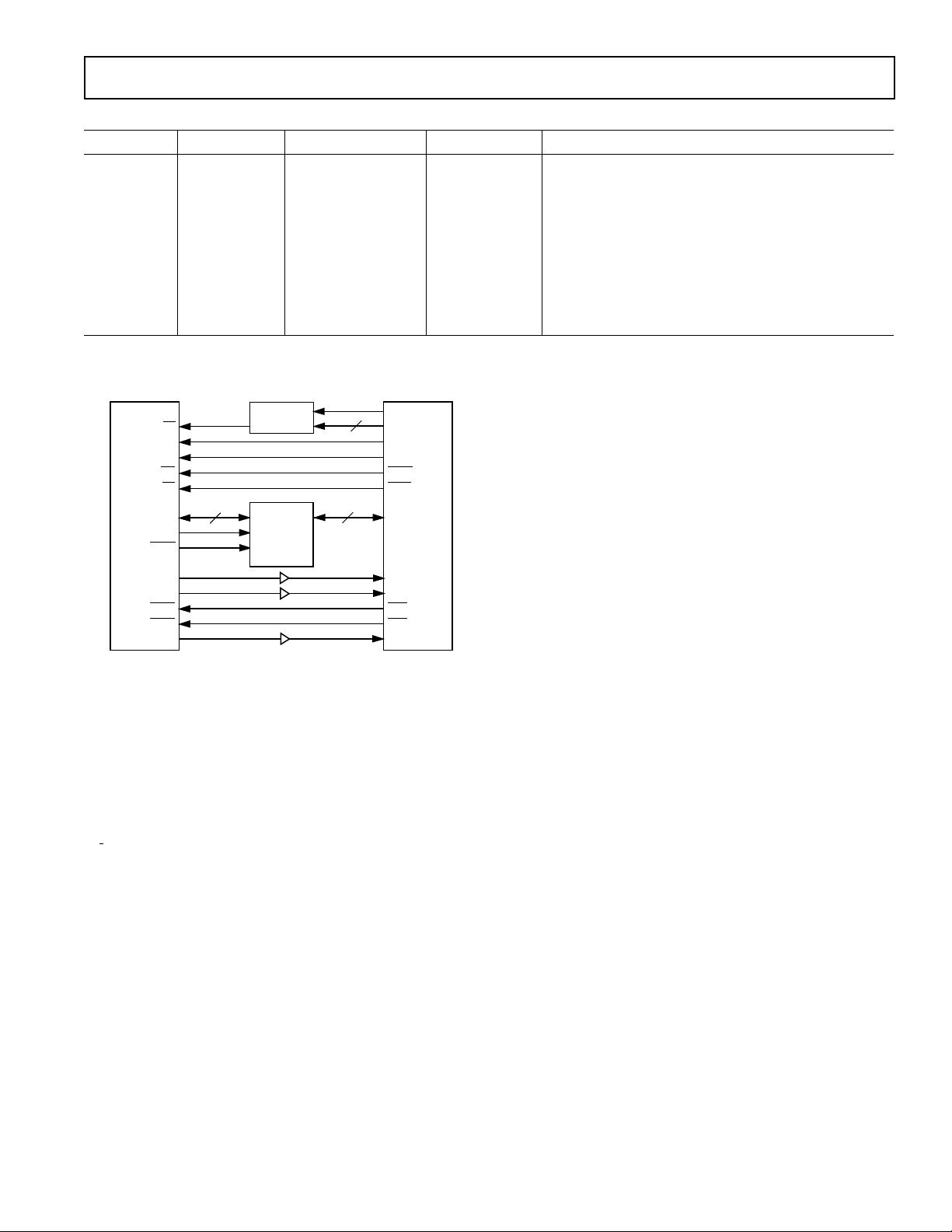
(Continued from page 1)
AD1845
AD1845
DATA7:0
DBDIR
DBEN
PDRQ
CDRQ
PDAK
CDAK
CS
A1
A0
WR
RD
INT
ADDRESS
DECODE
8
74_245
DIR
G
BA
AEN
18
SA19:2
SA1
SA0
IOWC
IORC
8
DATA7:0
DRQ <X>
DRQ <Y>
DAK <X>
DAK <Y>
IRQ <Z>
I
S
A
B
U
S
Figure 1. Interface to ISA Bus
External circuit requirements are limited to a minimal number
of low cost support components. Anti-imaging DAC output
filters are incorporated on-chip. Dynamic range exceeds 80dB
over the 20 kHz audio band. Sample rates from 4 kHz to 50kHz
are supported from a single external crystal or clock source.
The AD1845 has built-in 8/16 mA (user selectable) bus drivers.
If 24 mA drive capability is required, the AD1845 generates
enable and direction controls for IC bus buffers such as the
74
245.
The codec includes a stereo pair of ∑∆ analog-to-digital converters and a stereo pair of ∑∆ digital-to-analog converters. The
AD1845 mixer surpasses MPC Level-2 recommendations.
Inputs to the ADC can be selected from four stereo pairs of
analog signals: line (LINE), microphone (MIC), auxiliary line
#1 (AUX1), and post-mixed DAC output. A software-controlled programmable gain stage allows independent gain for
each channel going into the ADC. In addition, the analog mixer
allows the mono input (M_IN), MIC, AUX1, LINE and auxiliary line #2 (AUX2) signals to be mixed with the DACs’ output.
The ADCs’ output can be digitally mixed with the DACs’ input.
The pair of 16-bit outputs from the ADCs is available over a
byte-wide bidirectional interface that also supports 16-bit digital
input to the DACs and control information. The AD1845 can
accept and generate 16-bit twos complement PCM linear digital
data in both little endian or big endian byte ordering, 8-bit
unsigned magnitude PCM linear data, and 8-bit µ-law or A-law
companded digital data.
The ∑∆ DACs are preceded by a digital interpolation filter. An
attenuator provides independent user volume control over each
DAC channel. Nyquist images and shaped quantized noise are
removed from the DACs’ analog stereo output by on-chip
switched-capacitor and continuous-time filters.
The AD1845 supports multiple low power and power-down
modes to support notebook and portable computing multimedia
applications. The ADC, DAC, and mixer paths can be suspended independently allowing the AD1845 to be used for
capture-only or playback-only, lessening power consumption
and extending battery life.
The AD1845 includes a variable sample frequency generator,
that allows the codec to instantaneously change sample rates
with a resolution of 1 Hz without “clicks” and “pops.” Additionally, ∑∆ quantization noise is kept out of the 20 kHz audio
band regardless of the chosen sample rate. The codec uses the
variable sample frequency generator to derive all internal clocks
from a single external crystal or clock source.
Expanded Mode (MODE2)
MODE1 is the initial state of the AD1845. In this state the
AD1845 appears as an AD1848 compatible device. To access
the expanded modes of operation on the AD1845, the MODE2
bit should be set in the Miscellaneous Information Control
Register. When this bit is set to one, 16 additional indirect
registers can be addressed allowing the user to access the
AD1845’s expanded features. The AD1845 can return to
MODE1 operation by clearing the MODE2 bit. In both
MODE1 and MODE2, the capture and playback FIFOs are
active to prevent data loss.
The additional MODE2 functions are:
1. Full-Duplex DMA support.
2. MIC input mixer, mute and volume control.
3. Mono output with mute control.
4. Mono input with mixer volume control.
5. Software controlled advanced power-down modes.
6. Programmable sample rates from 4kHz to 50 kHz in 1 Hz
increments.
REV. C
–9–
Page 10

AD1845
FUNCTIONAL DESCRIPTION
This section overviews the functionality of the AD1845 and is
intended as a general introduction to the capabilities of the
device. As much as possible, detailed reference information has
been placed in “Control Registers” and other sections. The
user is not expected to refer repeatedly to this section.
Analog Inputs
The AD1845 SoundPort Stereo Codec accepts stereo line-level
and microphone-level inputs. The LINE, MIC, AUX1, and
post-mixed DAC output are available to the ADC multiplexer.
The DAC output can be mixed with LINE, MIC, AUX1,
AUX2 and M_IN. Each channel of the MIC inputs can be
amplified by +20 dB to compensate for the difference between
line levels and typical condenser microphone levels.
Analog Mixing
The M_IN mono input signal, MIC, LINE, AUX1 and AUX2
analog stereo signals can be mixed in the analog domain with
the DAC output. Each channel of each AUX, LINE and MIC
analog input can be independently gained/attenuated from
+12 dB to –34.5 dB in 1.5 dB steps or completely muted.
M_IN can be attenuated from 0 dB to –45 dB in 3 dB steps or
muted. The post-mixed DAC outputs are available on L_OUT
and R_OUT and also to the ADC input multiplexer.
Even if the AD1845 is not playing back data from its DACs, the
analog mix function can still be active.
Analog-to-Digital Datapath
The PGA following the input multiplexer allows independent
selectable gains for each channel from 0dB to 22.5dB in
+1.5 dB steps. The codec can operate either in a global stereo
mode or in a global mono mode with left-channel inputs
appearing at both channel outputs.
The AD1845 ∑∆ ADCs incorporate a fourth-order modulator.
A single pole of passive filtering is all that is required for antialiasing the analog input because of the ADC’s high over sampling ratio. The ADCs include linear-phase digital decimation
filters that low-pass filter the input to 0.4 × F
. (“FS” is the
S
word rate or “sampling frequency.”) ADC input over range
conditions are reported on status bits in the Test and Initialization Register.
Digital-to-Analog Datapath
The ∑∆ DACs are preceded by a programmable attenuator and
a low-pass digital interpolation filter. The anti-imaging interpolation filter over samples and digitally filters the higher frequency images. The attenuator allows independent control of
each DAC channel from 0 dB to –94.5 dB in –1.5 dB steps plus
full mute. The DACs’ ∑∆ noise shapers also over sample and
convert the signal to a single-bit stream. The DAC outputs are
then filtered in the analog domain by a combination of switchedcapacitor and continuous-time filters. They remove the very
high frequency components of the DAC bit stream output. No
external components are required.
Changes in DAC output attenuation take effect only on zero
crossings, eliminating “zipper” noise on playback. Each channel has its own independent zero-crossing detector and attenuator change control circuitry. A timer guarantees that requested
volume changes will occur even in the absence of a zero crossing. The time-out period is 8 milliseconds at a 48 kHz sampling
rate and 48 milliseconds at an 8 kHz sampling rate. (Timeout
[ms] ≈ 384 ÷ F
[kHz].)
S
Digital Mixing
Stereo digital output from the ADCs can be digitally mixed with
the input to the DACs. Digital output from the ADCs going out
of the data port is unaffected by the digital mix. Along the
digital mix datapath, the 16-bit linear output from the ADCs
is attenuated by an amount specified with control bits. Both
channels of the digital mix datapath are attenuated by the same
amount. (Note that internally the AD1845 always works with
16-bit PCM linear data, digital mixing included; format conversions take place at the input and output.)
Sixty-four steps of –1.5 dB attenuation are supported to –94.5dB.
The digital mix datapath can also be completely muted. Note
that the level of the mixed signal is also a function of the input
PGA settings, since they affect the ADCs’ output.
The attenuated digital mix data is digitally summed with the
DAC input data prior to the DACs’ datapath attenuators. The
digital sum of digital mix data and DAC input data is clipped at
plus or minus full scale and does not wrap around. Because both
stereo signals are mixed before the output attenuators, mix data is
attenuated a second time by the DACs’ datapath attenuators.
In case the AD1845 is capturing data, but ADC output data is
not removed in time (“ADC overrun”), the last sample captured
before overrun will be used for the digital mix. In case the
AD1845 is playing back data, but input digital DAC data fails
to arrive in time (“DAC underrun”), a midscale zero will be
added to the digital mix data when the DACZ control bit is set
to 0; otherwise, the DAC will output the previous valid sample
in an underrun condition.
Analog Outputs
Stereo and mono line-level outputs are available at external
pins. Each channel of this output can be independently muted.
When muted, the outputs will settle to a dc value near V
REF
, the
midscale reference voltage. The output is selectable for 2.0 V
peak-to-peak or 2.8 V peak-to-peak. When selecting the LINE
output as an input to the ADC, the ADC automatically compensates for the output level selection.
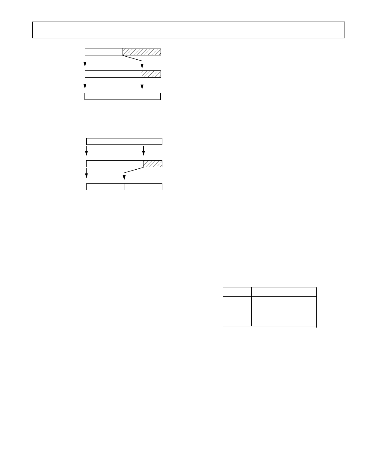
Digital Data Types
The AD1845 supports five global data types: 16-bit twos complement linear PCM (little endian and big endian byte ordering),
8-bit unsigned linear PCM, companded µ-law, and 8-bit com-
panded A-law, as specified by control register bits. Data in all
formats is always transferred MSB first. All data formats that are
less than 16 bits are MSB-aligned to ensure the use of full
system resolution.
The 16-bit PCM data format is capable of representing 96 dB
of dynamic range. Eight-bit PCM can represent 48 dB of dynamic range. Companded µ-law and A-law data formats use
nonlinear coding with less precision for large amplitude signals.
The loss of precision is compensated for by an increase in dynamic range to 64 dB and 72 dB, respectively.
On input, 8-bit companded data is expanded to an internal
linear representation, according to whether µ-law or A-law was
specified in the codec’s internal registers. Note that when µ-law
compressed data is expanded to a linear format, it requires
14 bits. A-law data expanded requires 13 bits.
–10–
REV. C
Page 11
AD1845
COMPRESSED
INPUT DATA
EXPANSION
DAC INPUT 000/00
15
MSB LSB
15
MSB LSB
15
MSB LSB
8 7
3/2 2/1
3/2 2/1
0
0
0
Figure 2. µ-Law or A-Law Expansion
When 8-bit companding is specified, the ADCs’ linear output is
compressed to the format specified.
ADC OUTPUT
TRUNCATION
COMPRESSION
15
MSB LSB
MSB LSB
15
MSB LSB
3/2 2/1
8 7
00000000
0
015
0
Figure 3.µ-Law or A-Law Compression
Note that all format conversions take place at input or output.
Internally, the AD1845 always uses 16-bit linear PCM representations to maintain maximum precision.
Timer Registers
The timer registers are provided for system level synchronization, and for periodic interrupt generation. The 16-bit timer
time base is determined by the frequency of the connected input
clock source.
The timer is enabled by setting the Timer Enable bit, TE, in the
Alternate Feature Enable register. To set the timer, load the
Upper and Lower Timer Bits Registers. The timer value will
then be loaded into an internal count register with a value of
approximately 10 µs (the exact timer value is listed in the regis-
ter descriptions). The internal count register will decrement
until it reaches zero, then the Timer Interrupt bit, TI, is set and
an interrupt will be sent to the host. The next timer clock will
load the internal count register with the value of the Timer
Register, and the timer will be reinitialized. To clear the interrupt, write to the Status Register or write a “0” to TI.
Interrupts
The AD1845 supports interrupt conditions generated by DMA
playback count expiration, DMA capture count expiration, or
timer expiration. The INT bit will remain set, HI, until a write
has been completed to the Status Register or by clearing the TI,
CI, or PI bit (depending on the existing condition) in the Capture Playback Timer Register. The IEN bit of the Pin Control
Register determines whether the interrupt pin responds to an
interrupt condition and reflects the interrupt state on the
INT status bit.
Power Supplies and Voltage Reference
The AD1845 operates from a +5 V power supply. Independent
analog and digital supplies are recommended for optimal performance though excellent results can be obtained in single-supply
systems. A voltage reference is included on the codec and its
2.25 V buffered output is available on an external pin (V
REF
).
The reference output can be used for biasing op amps used in
dc coupling. The internal reference is externally bypassed to
analog ground at the V
REF_F
pin.
Clocks and Sample Rates
The AD1845 operates from a single external crystal or clock
source. From a single input, a wide range of sample rates can be
generated. The AD1845 default frequency source is a
24.576 MHz input. The AD1845 can also be driven from a
14.31818 MHz (OSC), 24 MHz, 25 MHz or 33 MHz input
frequency source. In MODE1, the input drives the internal
variable sample frequency generator to derive the following
AD1848 compatible sample rates: 5.5125, 6.615, 8, 9.6,
11.025, 16, 18.9, 22.05, 27.42857, 32, 33.075, 37.8, 44.1,
48 kHz. In MODE2, the AD1845 can be programmed to generate any sample frequency between 4 kHz and 50kHz with
1 Hz resolution. Note that it is no longer required to enter
Mode Change Enable (MCE) to change the sample rate. This
feature allows the user to change the AD1845’s sample rate “on
the fly.”
CONTROL REGISTERS
Control Register Architecture
The AD1845 SoundPort Stereo Codec accepts both data and
control information through its byte-wide parallel port. Indirect
addressing minimizes the number of external pins required to
access all 37 of its byte-wide internal registers. Only two external address pins, ADR1:0, are required to accomplish all data
and control transfers. These pins select one of five direct registers. (ADR1:0 = 3 addresses two registers, depending on
whether the transfer is for a playback or capture.)
ADR1:0 Register Name
0 Index Address Register
1 Indexed Data Register
2 Status Register
3 PIO Data Register
Figure 4. Direct Register Map
REV. C
–11–
Page 12

AD1845
A write to or a read from the Indexed Data Register will access the Indirect Register which is indexed by the value most recently
written to the Index Address Register. The Status Register and the PIO Data Register are always accessible directly, without
indexing. The 32 Indirect Register indexes are shown in Figure 5:
Index Register Name Reset/Default State
0 Left Input Control 000x 0000
1 Right Input Control 000x 0000
2 Left Aux #1 Input Control 1xx0 1000
3 Right Aux #1 Input Control 1xx0 1000
4 Left Aux #2 Input Control 1xx0 1000
5 Right Aux #2 Input Control 1xx0 1000
6 Left Output Control 1x00 0000
7 Right Output Control 1x00 0000
8 Clock and Data Format 0000 0000
9 Interface Configuration 00xx 1000
10 Pin Control 00xx xx00
11 Test and Initialization 0000 0000
12 Miscellaneous Information 10x0 1010
13 Digital Mix/Attenuation 0000 00x0
14 Upper Base Count 0000 0000
15 Lower Base Count 0000 0000
16 Alternate Feature Enable/Left MIC Input Control 0001 0001
17 MIC Mix Enable/Right MIC Input Control 0001 000x
18 Left Line Gain, Attenuate, Mute, Mix 1xx0 1000
19 Right Line Gain, Attenuate, Mute, Mix 1xx0 1000
20 Lower Timer 0000 0000
21 Upper Timer 0000 0000
22 Upper Frequency Select 0001 1111
23 Lower Frequency Select 0100 0000
24 Capture Playback Timer x000 0000
25 Revision ID 100x x000
26 Mono Control 00xx 0011
27 Power-Down Control 000x 0xxx
28 Capture Data Format Control 0000 xxxx
29 Crystal Clock Select/Total Power-Down 000x xxx0
30 Capture Upper Base Count 0000 0000
31 Capture Lower Base Count 0000 0000
“x” indicates reserved bit, always write “0s” to these bits.
Figure 5. Indirect Register Map and Reset/Default States
A detailed map of all direct and indirect register contents is summarized for reference as follows:
–12–
REV. C
Page 13
Direct Registers
ADRl:0 Data 7 Data 6 Data 5 Data 4 Data 3 Data 2 Data 1 Data 0
0 INIT MCE TRD IXA4 IXA3 IXA2 IXA1 IXA0
1 IXD7 IXD6 IXD5 IXD4 IXD3 IXD2 IXD1 IXD0
2 CU/L CL/R CRDY SOUR PU/L PL/R PRDY INT
3 CD7 CD6 CD5 CD4 CD3 CD2 CD1 CD0
3 PD7 PD6 PD5 PD4 PD3 PD2 PD1 PD0
Indirect Registers
IXA3:0 Data 7 Data 6 Data 5 Data 4 Data 3 Data 2 Data 1 Data 0
0 LSS1 LSS0 LMGE res LIG3 LIG2 LIG1 LIG0
1 RSS1 RSS0 RMGE res RIG3 RIG2 RIG1 RIG0
2 LMX1 res res LX1A4 LX1A3 LX1A2 LX1A1 LX1A0
3 RMX1 res res RX1A4 RX1A3 RX1A2 RX1A1 RX1A0
4 LMX2 res res LX2A4 LX2A3 LX2A2 LX1A1 LX2A0
5 RMX2 res res RX2A4 RX2A3 RX2A2 RX2A1 RX2A0
6 LDM res LDA5 LDA4 LDA3 LDA2 LDA1 LDA0
7 RDM res RDA5 RDA4 RDA3 RDA2 RDA1 RDA0
8 FMT1 FMT0 C/L S/M CFS2 CFS1 CFS0 CSS
9 CPIO PPIO res res ACAL SDC CEN PEN
10 XCTL1 XCTL0 res res res res IEN INITD
11 COR PUR ACI DRS ORR1 ORR0 ORL1 ORL0
12 MID MODE2 BUF8 res ID3 ID2 ID1 ID0
13 DMA5 DMA4 DMA3 DMA2 DMA1 DMA0 res DME
14 UB7 UB6 UB5 UB4 UB3 UB2 UB1 UB0
15 LB7 LB6 LB5 LB4 LB3 LB2 LB1 LB0
Expanded Mode (Requires MODE2=1)
16 OL TE LMG4 LMG3 LMG2 LMG1 LMG0 DACZ
17 LMME RMME RMG4 RMG3 RMG2 RMG1 RMG0 res
18 LLM res res LLG4 LLG3 LLG2 LLG1 LLG0
19 RLM res res RLG4 RLG3 RLG2 RLG1 RLG0
20 TL7 TL6 TL5 TL4 TL3 TL2 TL1 TL0
21 TU7 TU6 TU5 TU4 TU3 TU2 TU1 TU0
22 FU7 FU6 FU5 FU4 FU3 FU2 FU1 FU0
23 FL7 FL6 FL5 FL4 FL3 FL2 FL1 FL0
24 res TI CI PI CU CO PO PU
25 V2 V1 V0 res res CID2 CID1 CID0
26 MIM MOM res res MIA3 MIA2 MIA1 MIA0
27 ADCPWD DACPWD MIXPWD res FREN res res res
28 CFMT1 CFMT0 CC/L CS/M res res res res
29 XFS2 XFS1 XFS0 res res res res TOTPWD
30 CUB7 CUB6 CUB5 CUB4 CUB3 CUB2 CUB1 CUB0
31 CLB7 CLB6 CLB5 CLB4 CLB3 CLB2 CLB1 CLB0
AD1845
Figure 6. Register Summary
Note that the only sticky bit in any of the AD1845 control registers is the interrupt (INT) bit. All other bits can change with every
sample period.
REV. C
–13–
Page 14

AD1845
DIRECT CONTROL REGISTER DEFINITIONS
Index Address Register (ADR1:0 = 0)
ADR1:0 Data 7 Data 6 Data 5 Data 4 Data 3 Data 2 Data 1 Data 0
0 INIT MCE TRD IXA4 IXA3 IXA2 IXA1 IXA0
IXA4:0 Index Address. These bits define the address of the AD1845 register accessed by the Indexed Data Register.
These bits are read/write. IXA4 is not active in MODE1. Always write 0 to this bit when using the AD1845 in
MODE1.
TRD Transfer Request Disable. This bit, when set, causes PIO and DMA transfers to cease when the Interrupt Status
(INT) bit of the Status Register is set.
0 Transfers Enabled During Interrupt. PDRQ and CDRQ pin outputs are generated uninhibited by interrupts.
DMA Current Counter Register decrements with every sample transferred when either PEN or CEN are enabled.
1 Transfers Disabled By Interrupt. PDRQ and CDRQ pin outputs are generated only if INT bit is 0 (when
either PEN or CEN, respectively are enabled). Any pending playback or capture requests are allowed to
complete at the time when INT is set. After pending requests complete, the data in the FIFO will be consumed at the sample rate. Subsequently, the midscale inputs will be internally generated for the DACs if
the DACZ bit is set, otherwise, the previous valid sample will be repeated, and the ADC output buffer will
contain the last valid output. Clearing the sticky INT bit (or the TRD bit) will cause the resumption of
playback and/or capture requests (presuming PEN and/or CEN are enabled). The DMA Current Counter
Register will not decrement while both the TRD bit is set and the INT bit is a one. No over run or under
run error will be reported when transfers are disabled by INT.
MCE Mode Change Enable. This bit must be set whenever the current functional mode of the AD1845 is changed
where noted in the Indirect Control Registers 8, 9, 28 and 29. MCE must be cleared at the completion of the
desired register changes.
The DAC outputs are automatically muted when the MCE bit is set. After MCE is cleared, the DAC outputs will
be restored to the state specified by the LDM and RDM mute bits.
Both ADCs and DACs are automatically muted for 32 sample cycles after exiting the MCE state to allow the refer-
ence and all filters to settle. The ADCs will produce midscale values; the DACs’ analog output will be muted. All
converters are internally operating during these 32 sample cycles, and the AD1845 will expect playback data and
will generate (midscale) capture data. Note that the autocalibrate-in-progress (ACI) bit will be set on exiting from
the MCE state only when ACAL is set. If ACAL bit is set, ACI will remain HI for these 384 sample cycles, allow-
ing system software to poll this bit rather than count cycles.
Special sequences must be followed if autocalibrate (ACAL) is set during mode change enable. See the
“Autocalibration” section.
INIT AD1845 Initialization. This bit is set when the AD1845 cannot respond to parallel bus cycles. This bit is
read-only.
Immediately after reset and once the AD1845 has left the INIT state, the initial value of this register will be “0100 0000 (40h).”
During AD1845 initialization, this register cannot be written and always reads “1000 0000 (80h).”
Indexed Data Register (ADR1:0 = 1)
ADR1:0 Data 7 Data 6 Data 5 Data 4 Data 3 Data 2 Data 1 Data 0
1 IXD7 IXD6 IXD5 IXD4 IXD3 IXD2 IXD1 IXD0
IXD7:0 Indexed Register Data. These bits contain the contents of the AD1845 register referenced by the Indexed Data
Register.
During AD1845 initialization, this register cannot be written and always reads as “1000 0000 (80h).”
–14–
REV. C
Page 15

AD1845
Status Register (ADR1:0 = 2)
ADR1:0 Data 7 Data 6 Data 5 Data 4 Data 3 Data 2 Data 1 Data 0
2 CU/L CL/R CRDY SOUR PU/L PL/R PRDY INT
INT Interrupt Status. This sticky bit (the only one) indicates the status of the interrupt logic of the AD1845. This bit
is cleared by any host write of any value to this register. The IEN bit of the Pin Control Register determines
whether the state of this bit is reflected on the INT pin of the AD1845. The only interrupt conditions supported
by the AD1845 are generated by the underflow of the DMA Current Count Register or the Timer Registers. The
Timer Register operates at a 10 µs resolution. Clearing INT requires a 10 µs wait. If an immediate clearing of a TI
condition is desired, clear the TE bit to remove the timer interrupt.
0 Interrupt pin inactive
1 Interrupt pin active
PRDY Playback Data Register Ready. The PIO or DMA Playback Data Register is ready for more data. This bit is intended
to be used when direct programmed I/O data transfers are desired; however, it is also valid for DMA transfers.
This bit is read-only.
0 DAC data is still valid. Do not overwrite.
1 DAC data is stale. Ready for next host data write value.
PL/R Playback Left/Right Sample. This bit indicates whether the PIO or DMA playback data needed is for the right
channel DAC or left channel DAC. This bit is read-only.
0 Right channel needed
1 Left channel or mono
PU/L Playback Upper/Lower Byte. This bit indicates whether the PIO or DMA playback data needed is for the upper or
lower byte of the channel. This bit is read-only.
0 Lower byte needed
1 Upper byte needed or any 8-bit mode
SOUR Sample Over/Underrun. This bit indicates that the most recent sample was not serviced in time and therefore
either a capture overrun (COR) or playback underrun (PUR) has occurred. The bit indicates an overrun for ADC
capture and an underrun for DAC playback. If both capture and playback are enabled, the source that set this bit
can be determined by reading COR and PUR. This bit changes on a sample by sample basis. This bit is read-only.
CRDY Capture Data Ready. The PIO Capture Data Register contains data ready for reading by the host. This bit
should only be used when direct programmed I/O data transfers are desired. This bit is read-only.
0 ADC data is stale. Do not reread the information.
1 ADC data is fresh. Ready for next host data read.
CL/R Capture Left/Right Sample. This bit indicates whether the PIO capture data waiting is for the right channel ADC
or left channel ADC. This bit is read-only.
0 Right channel
1 Left channel or mono
CU/L Capture Upper/Lower Byte. This bit indicates whether the PIO capture data ready is for the upper or lower byte
of the channel. This bit is read-only.
0 Lower byte ready
1 Upper byte ready or any 8-bit mode
The PRDY, CRDY, and INT bits of this status register can change asynchronously to host accesses. The host may access this register while the bits are transitioning. The host read may return a zero value just as these bits are changing, for example. A one value
would not be read until the next host access.
While the FIFOs have multiple samples available for transfer, the CRDY and PRDY status bits for consecutive samples are approximately 320 ns–600 ns apart.
This register’s initial state after reset is “1100 1100.”
REV. C
–15–
Page 16

AD1845
PIO Data Registers (ADR1:0 = 3)
ADR1:0 Data 7 Data 6 Data 5 Data 4 Data 3 Data 2 Data 1 Data 0
3 CD7 CD6 CD5 CD4 CD3 CD2 CD1 CD0
3 PD7 PD6 PD5 PD4 PD3 PD2 PD1 PD0
The PIO Data Registers are two registers mapped to the same address. Writes send data to the PIO Playback Data Register
(PD7:0). Reads will receive data from the PIO Capture Data Register (CD7:0).
During AD1845 initialization, the PIO Playback Data Register cannot be written to and the Capture Data Register is always read
as “1000 0000 (80h).”
CD7:0 PIO Capture Data Register. This is the control register where capture data is read during programmed I/O data
transfers.
The reading of this register will increment the capture byte state machine so that the following read will be from
the next appropriate byte in the sample. The exact byte which is next to be read can be determined by reading the
Status Register. Once all relevant bytes have been read, the state machine will stay pointed to the last byte of the
sample until a new sample is received from the ADCs. Once this has occurred, the state machine and Status
Register will point to the first byte of the sample.
PD7:0 PIO Playback Data Register. This is the control register where playback data is written during programmed I/O
data transfers.
Writing data to this register will increment the playback byte tracking state machine so that the following write will
be to the correct byte of the sample. Once all bytes of a sample have been written, subsequent byte writes to this
port are ignored. The state machine is reset when the current sample is sent to the DACs.
INDIRECT CONTROL REGISTER DEFINITIONS
The following control registers are accessed by writing index values to IXA3:0 in the Index Address Register (ADR1:0 = 0) followed
by a read/write to the Indexed Data Register (ADR1:0 = 1).
Left Input Control (IXA3:0 = 0)
IXA3:0 Data 7 Data 6 Data 5 Data 4 Data 3 Data 2 Data 1 Data 0
0 LSS1 LSS0 LMGE res LIG3 LIG2 LIG1 LIG0
LIG3:0 Left input gain select. The least significant bit of this gain select represents +1.5 dB. Maximum gain is +22.5dB.
res Reserved for future expansion. Always write a zero to this bit.
LMGE Left Input Microphone Gain Enable. This bit will enable the +20 dB gain of the left MIC input signal.
LSS1:0 Left Input Source Select. These bits select the input source for the left gain stage preceding the left ADC.
LSS1 LSS0 Left Input Source
0 0 Left Line Source Selected
0 1 Left Auxiliary 1 Source Selected
1 0 Left Microphone Source Selected
1 1 Left Line Post-Mixed DAC Output Source Selected
This register’s initial state after reset is “000x 0000.”
Right Input Control (IXA3:0 = 1)
IXA3:0 Data 7 Data 6 Data 5 Data 4 Data 3 Data 2 Data 1 Data 0
1 RSS1 RSS0 RMGE res RIG3 RIG2 RIG1 RIG0
RIG3:0 Right Input Gain Select. The least significant bit of this gain select represents +1.5 dB. Maximum gain is +22.5 dB.
res Reserved for future expansion. Always write a zero to this bit.
RMGE Right Input Microphone Gain Enable. This bit will enable the +20 dB gain of the right MIC input signal.
RSS1:0 Right Input Source Select. These bits select the input source for the right channel gain stage preceding the right
ADC.
–16–
REV. C
Page 17

AD1845
RSS1 RSS0 Right Input Source
0 0 Right Line Source Selected
0 1 Right Auxiliary 1 Source Selected
1 0 Right Microphone Source Selected
1 1 Right Post-Mixed DAC Output Source Selected
This register’s initial state after reset is “000x 0000.”
Left Auxiliary #1 Input Control (IXA3:0 = 2)
IXA3:0 Data 7 Data 6 Data 5 Data 4 Data 3 Data 2 Data 1 Data 0
2 LMX1 res res LX1A4 LX1A3 LX1A2 LX1A1 LX1A0
LX1A4:0 Left Auxiliary Input #1 Attenuate Select. The least significant bit of this gain/attenuate select represents 1.5 dB.
LX1A4:0 = 0 produces a +12 dB gain. LX1A4:0 = “01000” (8 decimal) produces 0 dB gain. Maximum attenua-
tion is –34.5 dB. See Figure 10.
res Reserved for future expansion. Always write zeros to these bits.
LMX1 Left Auxiliary #1 Mute. This bit, when set, will mute the left channel of the Auxiliary #1 input source. This bit
powers up set.
This register’s initial state after reset is “1xx0 1000.”
Right Auxiliary #1 Input Control (IXA3:0 = 3)
IXA3:0 Data 7 Data 6 Data 5 Data 4 Data 3 Data 2 Data 1 Data 0
3 RMX1 res res RX1A4 RX1A3 RX1A2 RX1A1 RX1A0
RX1A4:0 Right Auxiliary Input #1 Attenuate Select. The least significant bit of this gain/attenuate select represents
1.5 dB. RX1A4:0 = 0 produces a +12 dB gain. RX1A4:0 = “01000” (8 decimal) produces 0 dB gain. Maximum
attenuation is –34.5 dB. See Figure 10.
res Reserved for future expansion. Always write zeros to these bits.
RMX1 Right Auxiliary #1 Mute. This bit, when set, will mute the right channel of the Auxiliary #1 input source. This
bit powers up set.
This register’s initial state after reset is “1xx0 1000.”
Left Auxiliary #2 Input Control (IXA3:0 = 4)
IXA3:0 Data 7 Data 6 Data 5 Data 4 Data 3 Data 2 Data 1 Data 0
4 LMX2 res res LX2A4 LX2A3 LX2A2 LX2A1 LX2A0
LX2A4:0 Left Auxiliary Input #2 Attenuate Select. The least significant bit of this gain/attenuate select represents 1.5 dB.
LX2A4:0 = 0 produces a +12 dB gain. LX2A4:0 = “01000” (8 decimal) produces 0 dB gain. Maximum attenua-
tion is –34.5 dB. See Figure 10.
res Reserved for future expansion. Always write zeros to these bits.
LMX2 Left Auxiliary #2 Mute. This bit, when set to 1, will mute the left channel of the Auxiliary #2 input source. This
bit powers up set.
This register’s initial state after reset is “1xx0 1000.”
Right Auxiliary #2 Input Control (IXA3:0 = 5)
IXA3:0 Data 7 Data 6 Data 5 Data 4 Data 3 Data 2 Data 1 Data 0
5 RMX2 res res RX2A4 RX2A3 RX2A2 RX2A1 RX2A0
REV. C
–17–
Page 18

AD1845
RX2A4:0 Right Auxiliary Input #2 Attenuate Select. The least significant bit of this gain/attenuate select represents
1.5 dB. RX2A4:0 = 0 produces a +12 dB gain. RX2A4:0 = “01000” (8 decimal) produces 0 dB gain.
Maximum attenuation is –34.5 dB. See Figure 10.
res Reserved for future expansion. Always write zeros to these bits.
RMX2 Right Auxiliary #2 Mute. This bit, when set, will mute the right channel of the Auxiliary #2 input source. This bit
powers up set.
This register’s initial state after reset is “1xx0 1000.”
Left DAC Control (IXA3:0 = 6)
IXA3:0 Data 7 Data 6 Data 5 Data 4 Data 3 Data 2 Data 1 Data 0
6 LDM res LDA5 LDA4 LDA3 LDA2 LDA1 LDA0
LDA5:0 Left DAC Attenuate Select. The least significant bit of this gain/attenuate select represents 1.5 dB. Maximum
attenuation is –94.5 dB. See Figure 7.
res Reserved for future expansion. Always write a zero to this bit.
LDM Left DAC Mute. This bit, when set to 1, will mute the left DAC output. This bit powers up active.
This register’s initial state after reset is “1x00 0000.”
Right DAC Control (IXA3:0 = 7)
IXA3:0 Data 7 Data 6 Data 5 Data 4 Data 3 Data 2 Data 1 Data 0
7 RDM res RDA5 RDA4 RDA3 RDA2 RDA1 RDA0
RDA5:0 Right DAC Attenuate Select. The least significant bit of this gain/attenuate select represents 1.5 dB. Maximum
attenuation is –94.5 dB. See Figure 7.
res Reserved for future expansion. Always write a zero to this bit.
RDM Right DAC Mute. This bit, when set to 1, will mute the right DAC output. This bit powers up active.
This register’s initial state after reset is “1x00 0000.”
A5 A4 A3 A2 A1 A0 Mix Gain
0000001–1.0 dB
0000011–1.5 dB
0000101–3.0 dB
0000111–4.5 dB
0001001–6.0 dB
0001011–7.5 dB
0001101–9.0 dB
000111–10.5 dB
001000–12.0 dB
001001–13.5 dB
001010–15.0 dB
001011–16.5 dB
• ••••••
• ••••••
• ••••••
110100–78.0 dB
110101–79.5 dB
110110–81.0 dB
110111–82.5 dB
111000–84.0 dB
111001–85.5 dB
111010–87.0 dB
111011–88.5 dB
111100–90.0 dB
111101–91.5 dB
111110–93.0 dB
111111–94.5 dB
Figure 7. Mix Gain Level Setting: DAC
–18–
REV. C
Page 19

AD1845
Clock and Data Format Register (IXA3:0 = 8)
IXA3:0 Data 7 Data 6 Data 5 Data 4 Data 3 Data 2 Data 1 Data 0
8 FMT1 FMT0 C/L S/M CFS2 CFS1 CFS0 CSS
NOTE: Placing the AD1845 in the Mode Change Enable (MCE) state is not required when changing the sample rate. However,
changes to FMT[1:0], C/L, and S/M require MCE or setting PEN = 0.
CSS Clock Source Select. This bit in conjunction with CFS2:0 selects the audio sample rate frequency. See Figure 8
below. Note: MODE2 allows a wider range of sample rate frequencies to be selected by using the Frequency
Select Register (refer to Registers 22 and 23).
CFS2:0 Clock Frequency Divide Select. These bits in conjunction with CSS select the audio sample frequency.
CFS2 CFS1 CFS0 CSS Sample Rate
0 0 0 0 8.0 kHz
0 0 0 1 5.5125 kHz
0 0 1 0 16.0 kHz
0 0 1 1 11.025 kHz
0 1 0 0 27.42857 kHz
0 1 0 1 18.9 kHz
0 1 1 0 32.0 kHz
0 1 1 1 22.05 kHz
1 0 0 0 Reserved
1 0 0 1 37.8 kHz
1 0 1 0 Reserved
1 0 1 1 44.1 kHz
1 1 0 0 48.0 kHz
1 1 0 1 33.075 kHz
1 1 1 0 9.6 kHz
1 1 1 1 6.615 kHz
Figure 8. MODE1 Audio Sample Frequency Select
S/M Stereo/Mono Select. This bit determines how the audio data streams are formatted. Selecting stereo will result
with alternating samples representing left and right audio channels. Mono playback plays the same audio sample
on both channels. Mono capture only captures data from the left audio channel.
0 Mono
1 Stereo
C/L Companded/Linear Select. This bit selects between a linear digital representation of the audio signal or a nonlinear,
companded format for all input and output data. The type of linear PCM or the type of companded format is
defined by the FMT bits.
0 Linear PCM
1 Companded
FMT[1:0] Format Select. The bits define the format for all digital audio input and outputs based on the state of the C/L bit.
See Figure 9 for FMT and C/L bit settings that determine the audio data type format.
res Reserved for future expansion. Always write a zero to this bit.
This register’s initial state after reset is “0000 0000.”
FMT1 FMT0 C/L Audio Data Type
0
00 1 µ-Law, 8-Bit Companded
0 1 0 Linear, 16-Bit Twos-Complement PCM Little Endian
0 1 1 A-Law, 8-Bit Companded
1 0 0 Reserved
1 0 1 Reserved
1 1 0 Linear, 16-Bit Twos Complement Big Endian
1 1 1 Reserved
0 0 Linear, 8-Bit Unsigned PCM
REV. C
Figure 9. Digital Audio Data Type
–19–
Page 20

AD1845
Interface Configuration Register (IXA3:0 = 9)
IXA3:0 Data 7 Data 6 Data 5 Data 4 Data 3 Data 2 Data 1 Data 0
9 CPIO PPIO res res ACAL SDC CEN PEN
NOTE: Placing the AD1845 in the Mode Change Enable (MCE) state is not required when changing the CEN and PEN bits in this
register.
PEN Playback Enable. This bit will enable the playback of data in the format selected. The AD1845 will generate
PDRQ and respond to
grammed I/O (PIO) playback mode.
0 Playback disabled (PDRQ and PIO Playback Data Register inactive)
1 Playback enabled
CEN Capture Enable. This bit will enable the capture of data in the format selected. The AD1845 will generate
CDRQ and respond to
capture mode.
0 Capture disable (CDRQ and PIO Capture Data Register inactive)
1 Capture enable
SDC Single DMA Channel. This bit will force both capture and playback DMA requests to occur on the Playback
DMA channel. The Capture DMA CDRQ pin will be LO. This bit will allow the AD1845 to be used with only
one DMA channel. Simultaneous capture and playback cannot occur in this mode. Should both capture and
playback be enabled (CEN=PEN=1) in the mode, only playback will occur. See “Data and Control Transfers” for
further explanation.
0 Dual DMA channel mode
1 Single DMA channel mode
ACAL Autocalibrate Enable. This bit determines whether the AD1845 performs an autocalibration whenever the Mode
Change Enable (MCE) bit changes from HI to LO. See “Autocalibration” for a description of a complete
autocalibration sequence. Note that an autocalibration is forced whenever the
asserted LO then transitions HI regardless of the state of the ACAL bit.
0 No autocalibration
1 Autocalibration after mode change
res Reserved for future expansion. Always write zeros to these bits.
PPIO Playback PIO Enable. This bit determines whether the playback data is transferred via DMA or PIO.
0 DMA transfers only
1 PIO transfers only
CPIO Capture PIO Enable. This bit determines whether the capture data is transferred via DMA or PIO.
0 DMA transfers only
1 PIO transfers only
This register’s initial state after reset is “00xx 1000.”
PDAK signals when this bit is enabled and PPIO = 0. If PPIO = 1, this bit enables Pro-
CDAK signals when this bit is enabled and CPIO = 0. If CPIO = 1, this bit enables PIO
RESET or PWRDWN pin is
Pin Control Register (IXA3:0 = 10)
IXA3:0 Data 7 Data 6 Data 5 Data 4 Data 3 Data 2 Data 1 Data 0
10 XCTL1 XCTL0 res res res res IEN INITD
INITD Disable setting the INIT bit after changing the sample rate in MODE1. Otherwise the INIT bit is set HI for
approximately 200 µs after changing the sample rate.
0 INIT bit is enabled
1 INIT bit is disabled
IEN Interrupt Enable. This bit enables the interrupt pin. The Interrupt Pin will go active HI when the number of
samples programmed in the Base Count Register is reached.
0 Interrupt disabled
1 Interrupt enabled
res Reserved for future expansion. Always write zeros to these bits.
–20–
REV. C
Page 21

AD1845
XCTL1:0 External Control. The state of these bits is reflected on the XCTL1:0 pins of the AD1845.
0 Logic LO on XCTL1:0 pins
1 Logic HI on XCTL1:0 pins
This register’s initial state after reset is “00xx xx00.”
Test and Initialization Register (IXA3:0 = 11)
IXA3:0 Data 7 Data 6 Data 5 Data 4 Data 3 Data 2 Data 1 Data 0
11 COR PUR ACI DRS ORR1 ORR0 ORL1 ORL0
ORL1:0 Overrange Left Detect. These bits indicate the overrange on the left capture channel. These bits change on
a sample-by-sample basis, and are read-only.
ORL1 ORL0
0 0 Less than –1 dB underrange
0 1 Between –1 dB and 0 dB underrange
1 0 Between 0 dB and +1 dB overrange
1 1 Greater than +1 dB overrange
ORR1:0 Overrange Right Detect. These bits indicate the overrange on the right capture channel. These bits change
on a sample-by-sample basis, and are read-only.
ORR1 ORR0
0 0 Less than –1 dB underrange
0 1 Between –1 dB and 0 dB underrange
1 0 Between 0 dB and +1 dB overrange
1 1 Greater than +1 dB overrange
DRS Data Request Status. This bit indicates the current status of the PDRQ and CDRQ pins of the AD1845.
0 CDRQ and PDRQ are presently inactive (LO)
1 CDRQ or PDRQ are presently active (HI)
ACI Autocalibrate-In-Progress. This bit indicates the state of autocalibration or a recent exit from Mode Change
Enable (MCE). This bit is read-only.
0 Autocalibration is not in progress
1 Autocalibration is in progress or MCE was exited within the last 128 sample periods
PUR Playback Underrun. This bit is set when the playback FIFO is empty and after the next valid sample has been
played back. If this condition exists, DACZ determines the DAC playback value. In MODE1, DACZ is always set
and returns a midscale value.
COR Capture Overrun. This bit is set when the capture FIFO is full and an additional sample has been captured. The
sample being read will not be overwritten by the new sample. The new sample will be ignored. This bit changes on
a sample by sample basis.
The occurrence of a PUR and/or COR is designated in the Status Register’s Sample Overrun/Underrun (SOUR) bit. The SOUR bit
is the logical OR of the COR and PUR bits. This enables a polling host CPU to detect an overrun/underrun condition while checking other status bits.
This register’s initial state after reset is “0000 0000.”
Miscellaneous Control Register (IXA3:0 = 12)
IXA3:0 Data 7 Data 6 Data 5 Data 4 Data 3 Data 2 Data 1 Data 0
12 MID MODE2 res BUF8 ID3 ID2 ID1 ID0
ID3:0 AD1845 Revision ID. These four bits define the revision level of the AD1845. The AD1845 will have ID =
“1010.” These bits are read-only.
BUF8 Parallel Interface Bus Transceiver Current Buffer Drive. The AD1845 can be programmed to provide a current
drive of 16 mA or 8 mA.
0 16 mA current drive.
1 8 mA current drive.
res Reserved for future expansion. Always write 0s to these bits.
REV. C
–21–
Page 22

AD1845
MODE2 When the AD1845 is initialized, the MODE2 bit is set to 0, LO, and the AD1845 is register set compatible with
the AD1848 and the AD1846. Setting the MODE2 bit to 1, HI, enables access to the indirect registers 16
through 31 which controls the AD1845 Expanded Mode of operation.
0 MODE1: AD1848, AD1846, and CS4248 mode
1 MODE2: AD1845 enhanced feature mode
MID Manufacturer ID Bit. This bit is set to 1.
This register’s initial state after reset is “10x0 1010.”
Digital Mix/Attenuation Control Register (IXA3:0 = 13)
IXA3:0 Data 7 Data 6 Data 5 Data 4 Data 3 Data 2 Data 1 Data 0
13 DMA5 DMA4 DMA3 DMA2 DMA1 DMA0 res DME
DME Digital Mix Enable. This bit will enable the digital mix of the ADC’s output with the DAC’s input. When en-
abled, the data from the ADCs are digitally mixed with other data being delivered to the DACs regardless of
whether or not playback is enabled (PEN = 1). If capture is enabled (CEN = 1) and there is a capture overrun
(COR), then the last sample captured before overrun will be used for the digital mix. If playback is enabled
(PEN = 1) and there is a playback underrun (PUR), then a midscale zero will be added to the digital mix data if
DACZ = 1, otherwise, the last valid sample will be repeated.
0 Digital mix disabled (muted)
1 Digital mix enabled
res Reserved for future expansion. Always write a zero to this bit.
DMA5:0 Digital Mix Attenuation. These bits determine the attenuation of the ADC data that is mixed with the DAC in-
put. Each attenuate step is –1.5 dB ranging from 0 dB to –94.5 dB.
This register’s initial state after reset is “0000 00x0.”
DMA Playback Base Count Registers (IXA3:0 = 14 & 15)
The DMA Base Count Registers in the AD1845 simplify integration of the AD1845 in ISA systems. The ISA DMA controller requires an external count mechanism to notify the host CPU via interrupt of a full DMA buffer. The programmable DMA Base
Count Registers will allow such interrupts to occur.
The Base Count Registers contain the number of samples to be transferred before an interrupt is generated on the interrupt (INT)
pin. To load, first write a value to the Lower Base Count Register. Writing a value to the Upper Base Register will cause both Base
Count Registers to load into the Current Count Register. Once AD1845 transfers are enabled, each sample transferred causes the
Current Count Register to decrement until zero count is reached. The next sample after zero will generate the interrupt and reload
the Current Count Register with the values in the Base Count Registers. The interrupt is cleared by a write to the Status Register.
The Host Interrupt Pin (INT) will go HI during the sample period in which the Current Count Register underflows.
When using the AD1845 in MODE1 (AD1848 compatible), the Current Count Register is decremented every sample period when
either the PEN or CEN bit is enabled. The Current Count Register is decremented in both PIO and DMA data transfer modes.
Interrupt conditions are generated by Current Count Register underflows in both PIO and DMA transfers.
Program maximum value to the Upper Base Count Register to avoid receiving DMA count interrupts while operating in PIO mode.
By enabling MODE2, the AD1845 Expanded Mode, the playback counter is only decremented when a playback sample transfer occurs.
Upper Base Count Register (IXA3:0 = 14)
IXA3:0 Data 7 Data 6 Data 5 Data 4 Data 3 Data 2 Data 1 Data 0
14 UB7 UB6 UB5 UB4 UB3 UB2 UB1 UB0
UB7:0 Upper Base Count. This byte is the upper byte of the base count register containing the eight most significant bits
of the 16-bit base register. Reads from this register return the same value which was written. The current count
contained in the counters can not be read.
This register’s initial state after reset is “ 0000 0000.”
–22–
REV. C
Page 23

AD1845
Lower Base Count Register (IXA3:0 = 15)
IXA3:0 Data 7 Data 6 Data 5 Data 4 Data 3 Data 2 Data 1 Data 0
15 LB7 LB6 LB5 LB4 LB3 LB2 LB1 LB0
LB7:0 Lower Base Count. This byte is the lower byte of the base count register containing the eight least significant bits
of the 16-bit base register. Reads from this register return the same value which was written. The current count
contained in the counters cannot be read.
This register’s initial state after reset is “0000 0000.”
Expanded Modes (MODE2 = 1)
The following registers are enabled when the AD1845 is operating in MODE2 only.
Alternate Feature Enable/Left MIC Input Control Register (IXA3:0 = 16)
IXA3:0 Data 7 Data 6 Data 5 Data 4 Data 3 Data 2 Data 1 Data 0
16 OL TE LMG4 LMG3 LMG2 LMG1 LMG0 DACZ
DACZ DAC Zero. When an underrun error occurs, this bit will force the DAC output to midscale.
0 Output previous valid sample
1 Output to midscale value
LMG4:0 Left MIC Gain. The least significant bit of this gain/attenuate select represents 1.5 dB. LMG4:0 = 0 produces
a +12 dB gain. LMG4:0 = “01000” (8 decimal) produces 0 dB gain. Maximum attenuation is –34.5 dB.
See Figure 10.
TE Timer Enable. Setting this bit enables the 16-bit programmable timer (see Registers 20 and 21). When the timer
is enabled, the timer count is reloaded, and interrupts are generated at specified periods on the INT pin. When the
timer is disabled, the timer stops counting and the INT pin and TI bit are cleared immediately.
OL Output Level. This bit sets the analog output level. The line output level may be attenuated by 3 dB.
0 Full scale of 2.0 V p-p (–3 dB)
1 Full scale of 2.8 V p-p (0 dB)
This register’s initial state after reset is “0001 0001.”
MIC Mix Enable/Right MIC Input Control Register (IXA3:0 = 17)
IXA3:0 Data 7 Data 6 Data 5 Data 4 Data 3 Data 2 Data 1 Data 0
17 LMME RMME RMG4 RMG3 RMG2 RMG1 RMG0 res
res Reserved for future expansion. Always write zero to this bit.
RMG4:0 Right MIC Gain. The least significant bit of this gain/attenuate select represents 1.5 dB. RMG4:0 = 0 produces a
+12 dB gain. RMG4:0 = “01000” (8 decimal) produces 0 dB gain. Maximum attenuation is –34.5 dB.
See Figure 10.
RMME Right MIC Mix Enable. Setting this bit enables the right microphone input to be mixed with the DAC output on
R_OUT.
LMME Left MIC Mix Enable. Setting this bit enables the left microphone input to be mixed with the DAC output on
L_OUT.
This register’s initial state after reset is “0001 000x.”
Left Line Gain, Attenuate, Mute Mix Register (IXA3:0 = 18)
IXA3:0 Data 7 Data 6 Data 5 Data 4 Data 3 Data 2 Data 1 Data 0
18 LLM res res LLG4 LLG3 LLG2 LLG1 LLG0
LLG4:0 Left Line Mix Gain. Allows setting the left line mix gain in thirty-two 1.5 dB steps. See Figure 10 for mix gain
level setting.
res Reserved for future expansion. Always write zeros to these bits.
REV. C
–23–
Page 24

AD1845
LLM Left Line Mute. Setting this bit to 1 mutes the left line input into the output mixer.
This register’s initial state after reset is “1xx0 1000.”
Right Line Gain, Attenuate, Mute, Mix Register (IXA3:0 = 19)
IXA3:0 Data 7 Data 6 Data 5 Data 4 Data 3 Data 2 Data 1 Data 0
19 RLM res res RLG4 RLG3 RLG2 RLG1 RLG0
RLG4:0 Right Line Mix Gain. Allows setting the right line mix gain in thirty-two 1.5 dB steps. See Figure 10 for mix
gain level setting.
res Reserved for future expansion. Always write zeros to these bits.
RLM Right Line Mute. Setting this bit to 1 mutes the right line input into the output mixer.
This register’s initial state after reset is “1xx0 1000.”
A4/G4 A3/G3 A2/G2 A1/G1 A0/G0 Mix Gain
0 0 0 0 0 +12.0 dB
0 0 0 0 1 +10.5 dB
0 0 0 1 0 +9.0 dB
0 0 0 1 1 +7.5 dB
0 0 1 0 0 +6.0 dB
0 0 1 0 1 +4.5 dB
0 0 1 1 0 +3.0 dB
0 0 1 1 1 +1.5 dB
0 1 0 0 0 +0.0 dB
0 1 0 0 1 –1.5 dB
0 1 0 1 0 –3.0 dB
0 1 0 1 1 –4.5 dB
0 1 1 0 0 –6.0 dB
0 1 1 0 1 –7.5 dB
0 1 1 1 0 –9.0 dB
0 1 1 1 1 –10.5 dB
1 0 0 0 0 –12.0 dB
1 0 0 0 1 –13.5 dB
1 0 0 1 0 –15.0 dB
1 0 0 1 1 –16.5 dB
1 0 1 0 0 –18.0 dB
1 0 1 0 1 –19.5 dB
1 0 1 1 0 –21.0 dB
1 0 1 1 1 –22.5 dB
1 1 0 0 0 –24.0 dB
1 1 0 0 1 –25.5 dB
1 1 0 1 0 –27.0 dB
1 1 0 1 1 –28.5 dB
1 1 1 0 0 –30.0 dB
1 1 1 0 1 –31.5 dB
1 1 1 1 0 –33.0 dB
1 1 1 1 1 –34.5 dB
Figure 10. Mix Gain Level Setting: AUX1, AUX2, MIC and LINE
Lower Timer Bits Register (IXA3:0 = 20)
IXA3:0 Data 7 Data 6 Data 5 Data 4 Data 3 Data 2 Data 1 Data 0
20 TL7 TL6 TL5 TL4 TL3 TL2 TL1 TL0
TL7:0 Lower Timer Bits. This byte is the lower byte of the timer register containing the eight least significant bits of the
16-bit register. Reads from this register return the same value which was written. The current timer value contained in the counters cannot be read.
This register’s initial state after reset is “0000 0000.”
–24–
REV. C
Page 25

AD1845
Upper Timer Bits Register (IXA3:0 = 21)
IXA3:0 Data 7 Data 6 Data 5 Data 4 Data 3 Data 2 Data 1 Data 0
21 TU7 TU6 TU5 TU4 TU3 TU2 TU1 TU0
TU7:0 Upper Timer Bits. This byte is the upper byte of the timer register containing the eight most significant bits of the
16-bit register. Reads from this register return the same value which was written. The current timer value contained in the counters cannot be read. The timer counter is determined by the clock source selected (see below).
Input Frequency Divider Timer Counter
24.576 MHz 247 10.050 µs
14.31818 MHz 144 10.057 µs
24.000 MHz 242 10.083 µs
25.000 MHz 252 10.080 µs
33.000 MHz 333 10.091 µs
This register’s initial state after reset is “0000 0000.”
Upper Frequency Select Bits Register (IXA3:0 = 22)
IXA3:0 Data 7 Data 6 Data 5 Data 4 Data 3 Data 2 Data 1 Data 0
22 FU7 FU6 FU5 FU4 FU3 FU2 FU1 FU0
FU7:0 Upper Frequency Select Bits. This register is accessible when FREN is 1. Writing to this register allows the user
to program the sampling frequency from 4 kHz to 50 kHz in 1 Hz increments. Writing to the Lower and Upper
Frequency Select Register allows the AD1845 to process audio data using approximately 50,000 different audio
sample rates. One LSB represents exactly one hertz. Selecting frequencies below 4 kHz or above 50 kHz will
result in degraded audio performance. Some common sample rates are listed below:
Quality Sampling Frequency FU7:0 (hex) FL7:0 (hex)
Voice 8.0 kHz 0001 1111 0100 0000 default
Radio 11.025 kHz 0010 1011 0001 0001
Tape 22.05 kHz 0101 0110 0010 0010
CD 44.1 kHz 1010 1100 0100 0100
DAT 48.0 kHz 1011 1011 1000 0000
This register’s initial state after reset is “0001 1111.”
Lower Frequency Select Bits Register (IXA3:0 = 23)
IXA3:0 Data 7 Data 6 Data 5 Data 4 Data 3 Data 2 Data 1 Data 0
23 FL7 FL6 FL5 FL4 FL3 FL2 FL1 FL0
FL7:0 Lower Frequency Select Bits. Writing to the Lower Frequency Select register updates the entire 16-bit frequency register.
This register’s initial state after reset is “0100 0000.”
Capture Playback Timer Register (IXA3:0 = 24)
IXA3:0 Data 7 Data 6 Data 5 Data 4 Data 3 Data 2 Data 1 Data 0
24 res TI CI PI CU CO PO PU
PU Playback Underrun. This bit is set when the DAC runs out of data and a sample has been missed.
PO Playback Overrun. This bit is set when the host tries to write data into the FIFO and the write was ignored be-
cause the FIFO was full.
CO Capture Overrun. This bit is set when the ADC has a sample to load into the FIFO, and the data was ignored
because the capture FIFO was full.
CU Capture Underrun. This bit is set when the host attempts to read from the capture FIFO when it is empty. Under
these circumstances, the last valid byte is sent to the host.
PI Playback Interrupt. This bit indicates that there is an interrupt pending from the playback DMA count registers.
CI Capture Interrupt. This bit indicates that there is an interrupt pending from the capture DMA count registers.
REV. C
–25–
Page 26

AD1845
TI Timer Interrupt. This bit indicates that there is an interrupt pending from the timer count registers.
res Reserved for future expansion. Always write zero to this bit.
Playback, Capture and timer interrupts may be cleared simultaneously by writing to the Status Register. These interrupts may be
cleared individually by writing a “0” to the corresponding bit. Note that the timer interrupt requires a minimum wait period of 10 µs
after the interrupt is set and before TI is recognized. Use TE to clear the timer interrupt immediately.
This register’s initial state after reset is “100x x000.”
Revision ID Register (IXA3:0 = 25)
IXA3:0 Data 7 Data 6 Data 5 Data 4 Data 3 Data 2 Data 1 Data 0
25 V2 V1 V0 res res CID2 CID1 CID0
V2:0 Version Number. Indicates the version of the AD1845.
res Reserved for future expansion. Always write zeros to these bits.
CID2:0 Chip ID Number.
This register’s initial state after reset is “x000 0000.”
Mono Control Registers (IXA3:0 = 26)
IXA3:0 Data 7 Data 6 Data 5 Data 4 Data 3 Data 2 Data 1 Data 0
26 MIM MOM res res MIA3 MIA2 MIA1 MIA0
MIA3:0 Mono Input Attenuation. The least significant bit represents 3.0 dB attenuation. See Figure 11 to determine
the attenuation.
res Reserved for future expansion. Always write zeros to these bits.
MOM Mono Output Mute. M_OUT is muted by setting MOM to 1.
0 Mono output not muted
1 Mono output muted
MIM Mono Input Mute. M_IN is muted by setting MIM to 1.
0 Mono input not muted
1 Mono input muted
This register’s initial state after reset is “00xx 0011.”
MIA3 MIA2 MIA1 MIA0 MONO Attenuation
0 0 0 0 0.0 dB
0 0 0 1 –3.0 dB
0 0 1 0 –6.0 dB
0 0 1 1 –9.0 dB
0 1 0 0 –12.0 dB
0 1 0 1 –15.0 dB
0 1 1 0 –18.0 dB
0 1 1 1 –21.0 dB
1 0 0 0 –24.0 dB
1 0 0 1 –27.0 dB
1 0 1 0 –30.0 dB
1 0 1 1 –33.0 dB
1 1 0 0 –36.0 dB
1 1 0 1 –39.0 dB
1 1 1 0 –42.0 dB
1 1 1 1 –45.0 dB
Figure 11. Mono Attenuation
–26–
REV. C
Page 27

Power-Down Control Register (IXA3:0 = 27)
IXA3:0 Data 7 Data 6 Data 5 Data 4 Data 3 Data 2 Data 1 Data 0
AD1845
27
ADCPWD DACPWD MIXPWD
res
FREN
res res res
res Reserved for future expansion. Always write zeros to these bits.
FREN Frequency Select Register Enable. In MODE2, selecting this bit will turn on the Frequency Select Registers (see
indirect registers 22 and 23) and disable CFS2:0.
0 CFS Active.
1 Frequency Select Registers Active, CFS disabled.
MIXPWD Mixer Power Down. The DAC and the output mixer are powered down, and the DAC sample clock is turned off.
DACPWD DAC Power Down. The DAC is powered down and the DAC sample clock is turned off.
ADCPWD ADC Power Down. The ADC is powered down and the ADC sample clock is turned off.
This register’s initial state after reset is “000x 0xxx.”
Capture Data Format Control Register (IXA3:0 = 28)
IXA3:0 Data 7 Data 6 Data 5 Data 4 Data 3 Data 2 Data 1 Data 0
28 CFMT1 CFMT0 CC/L CS/M res res res res
NOTE: Changing CFMT[1:0], CC/L, CS/M, requires the Mode Change Enable (MCE) state or setting CEN = 0.
res Reserved for future expansion. Always write zeros to these bits.
CS/M Capture Stereo/Mono Select. Setting this bit determines how the captured audio data will be formatted. In the
Mono mode, valid information is captured on the “left” channel, and the “right” channel data is not valid.
0 Mono Format
1 Stereo Format
CC/L Capture Companding/Linear Select. This bit is set to determine linear, µ-Law or A-Law companding. See Figure
12 for CFMT[1:0] and CC/L bit settings that determine the audio data type capture format.
CFMT[1:0] Capture Data Format. This bit is set to format the data being captured in MODE 2. See Figure 12 for CFMT
and CC/L bit settings that determine the capture audio data type format.
This register’s initial state after reset is “0000 xxxx.”
CFMT1 CFMT0 CC/L Audio Data Type
0 0 0 Linear, 8-Bit Unsigned PCM
001 µ-Law, 8-Bit Companded
0 1 0 Linear, 16-Bit Twos Complement PCM Little Endian
0 1 1 A-Law, 8-Bit Companded
1 0 0 Reserved
1 0 1 Reserved
1 1 0 Linear, 16-Bit Twos-Complement Big Endian
1 1 1 Reserved
Figure 12. Capture Audio Data Type
Crystal, Clock Select/Total Power-Down Register (IXA3:0 = 29)
IXA3:0 Data 7 Data 6 Data 5 Data 4 Data 3 Data 2 Data 1 Data 0
29 XFS2 XFS1 XFS0 res res res res
TOTPWD
TOTPWD Total Power Down. When TOTPWD = HI, the ADC, DAC, mixer, and voltage reference are powered down, and
the ADC and DAC sample clocks are turned off. Only the digital interface remains active to allow the host to exit
the AD1845 from the total power-down state.
res Reserved for future expansion. Always write zeros to these bits.
REV. C
–27–
Page 28

AD1845
XFS2:0 Crystal/Clock Input Frequency Select. On power up or reset, the AD1845 expects a 24.576 MHz input clock. If
the clock source connected to the AD1845 is different from the default condition, then the clock input must be
selected using this register. For a detailed explanation see the Power Up and Reset section of the data sheet. Figure
13 summarizes the valid input clock frequencies. Clock sources with excessive jitter may not yield optimal analog
performance.
This register’s initial state after reset is “000x xxx0.”
XFS2 XFS1 XFS0 Input Frequency
0 0 0 24.576 MHz
0 0 1 14.31818 MHz
0 1 0 24.000 MHz
0 1 1 25.000 MHz
1 0 0 33.000 MHz
1 0 1 Reserved
1 1 0 Reserved
1 1 1 Reserved
Figure 13. Input Frequency Selection
Capture Upper Base Count Register (IXA3:0 = 30)
IXA3:0 Data 7 Data 6 Data 5 Data 4 Data 3 Data 2 Data 1 Data 0
30 CUB7 CUB6 CUB5 CUB4 CUB3 CUB2 CUB1 CUB0
CUB7:0 Capture Upper Base Count. This byte is the upper byte of the base count register containing the eight most sig-
nificant bits of the second 16-bit base register. Reads from this register return the same value that was written.
The current count contained in the counters cannot be read.
This register’s initial state after reset is “0000 0000.”
Capture Lower Base Count Register (IXA3:0 = 31)
IXA3:0 Data 7 Data 6 Data 5 Data 4 Data 3 Data 2 Data 1 Data 0
31 CLB7 CLB6 CLB5 CLB4 CLB3 CLB2 CLB1 CLB0
CLB7:0 Capture Lower Base Count. This byte is the lower byte of the base count register containing the eight least signifi-
cant bits of the second 16-bit base register. Reads from this register return the same value that was written. The
current count contained in the counters cannot be read.
This register’s initial state after reset is “0000 0000.”
–28–
REV. C
Page 29

AD1845
DATA AND CONTROL TRANSFERS
The AD1845 SoundPort Stereo Codec supports a DMA request/grant architecture for transferring data with the host computer bus. One or two DMA channels can be supported.
Programmed I/O (PIO) mode is also supported for control
register accesses and for applications lacking DMA control.
PIO transfers can be made on one channel while the other is
performing DMA. Transfers to and from the AD1845
SoundPort Codec are asynchronous relative to the internal data
conversion clock. Transfers are buffered by FIFOs located in
the capture and playback paths.
Data Ordering
The number of byte-wide transfers required depends on the
data format selected. The AD1845 is designed for “little and
big endian” formats. In little endian format, the least significant
byte (i.e., occupying the lowest memory address) gets transferred first. Therefore, 16-bit data transfers require first transferring the least significant bits [7:0] and then transferring the
most significant bits [15:8], where Bit 15 is the most significant
bit in the word. In big endian format, byte ordering for the most
significant (MS) byte and least significant (LS) byte are swapped.
In addition, left channel data is always transferred before right
channel data with the AD1845. The following figures should
make these requirements clear.
TIME
SAMPLE 6 SAMPLE 5 SAMPLE 4 SAMPLE 3 SAMPLE 2 SAMPLE 1
TIME
SAMPLE 3 SAMPLE 3 SAMPLE 2 SAMPLE 2 SAMPLE 1 SAMPLE 1
RIGHT MS RIGHT LS LEFT MS LEFT LS
BYTES 3 AND 4 BYTES 1 AND 2
Figure 17. 16-Bit Stereo Data Stream Sequencing, Little
Endian
TIME
SAMPLE 6 SAMPLE 5 SAMPLE 4 SAMPLE 4 SAMPLE 3 SAMPLE 2 SAMPLE 1
LS MS LS MS
BYTES 3 AND 4 BYTES 1 AND 2
Figure 18. 16-Bit Mono Data Stream Sequencing, Big
Endian
TIME
SAMPLE 3 SAMPLE 3 SAMPLE 2 SAMPLE 2 SAMPLE 1 SAMPLE 1
RIGHT LS RIGHT MS LEFT LS LEFT MS
BYTES 3 AND 4 BYTES 1 AND 2
Figure 19. 16-Bit Stereo Data Stream Sequencing, Big
Endian
MONO MONO MONO MONO
BYTE 4 BYTE 3 BYTE 2 BYTE 1
Figure 14. 8-Bit Mono Data Stream Sequencing
TIME
SAMPLE 3 SAMPLE 3 SAMPLE 2 SAMPLE 2 SAMPLE 1 SAMPLE 1
RIGHT LEFT
BYTE 4 BYTE 3 BYTE 2 BYTE 1
RIGHT LEFT
Figure 15. 8-Bit Stereo Data Stream Sequencing
TIME
SAMPLE 6 SAMPLE 5 SAMPLE 4 SAMPLE 3 SAMPLE 2 SAMPLE 1
LS MS LS MS
BYTES 3 AND 4 BYTES 1 AND 2
Figure 16. 16-Bit Mono Data Stream Sequencing, Little
Endian
FIFO
The AD1845 includes two 16-sample deep FIFOs. The FIFOs
are built into the capture and playback paths and are completely
transparent to the user and require no programming. The
FIFOs are active in MODE1 and MODE2.
The AD1845 maintains a continuous playback stream by requesting data from the host until the FIFO located in the playback path is full. As the FIFO empties, new samples are
requested to keep the playback FIFO full. In the event that the
FIFO runs out of data and DACZ is reset to “0,” the last valid
sample will be continuously played back. If DACZ is “1,” the
AD1845 will output a midscale value.
The FIFO located in the capture data path attempts to stay
empty by making requests of the host every sample period that it
contains valid data. When the host system cannot respond
during the same sample period, the capture FIFO starts filling,
and avoids a loss of data in the audio data stream.
Data Bus Drivers
The AD1845 has built-in 8 or 16 mA bus drivers for interfacing
to the ISA bus. The drivers reduce the need for the off-chip
74_245 bus transceiver buffers in many applications. If higher
drive capability is required, 24 mA for example, the AD1845
generates the appropriate direction and enable signals. See
Figure 1 and refer to the Applications Circuits section of the
data sheet.
Control and Programmed I/O (PIO) Transfers
This simpler mode of transfers is used both for control register
accesses and programmed I/O. The 37 control and PIO data
registers cannot be accessed via DMA transfers. Playback PIO
REV. C
–29–
Page 30
AD1845
is activated when both Playback Enable (PEN) is set and Playback PIO (PPIO) is set. Capture PIO is activated when both
Capture Enable (CEN) is set and Capture PIO (CPIO) is set.
See Figures 20 and 21 for the detailed timing of the control
register/PIO transfers. The
RD and WR signals are used to
define the actual read and write cycles, respectively. The host
holds
CS LO during these transfers. The DMA Capture Data
Acknowledge (
(
PDAK) must be held inactive, i.e., HI.
CDAK) and Playback Data Acknowledge
For read/capture cycles, the AD1845 will place data on the
DATA7:0 lines while the host is asserting the read strobe,
RD,
by holding it LO. For write/playback, the host must place data
on the DATA7:0 pins while strobing the
WR signal LO. The
AD1845 latches the write/playback data on the rising edge of
the
WR strobe.
When using PIO data transfers, the Status Register must be
polled to determine when data should be transferred. Note that
the ADC capture data will be ready (CRDY HI) from the previous sample period shortly before the DAC playback data is
ready (PRDY HI) for the next sample period. The user should
not wait for both ADCs and DACs to become ready before
initiating data transfers. Instead, as soon as capture data is
ready, it should be read; as soon as the DACs are ready, playback data should be written.
Values written to the XCTL1:0 bits in the Pin Control Register
(IXA3:0 = 10) will be reflected in the state of the XCTL1:0
external output pins. This feature allows a simple method for
signaling or software control of external logic. Changes in state
of the external XCTL pins will occur within one sample period.
Because their change is referenced to the internal sample clock,
no useful timing diagram can be constructed.
DIRECT MEMORY ACCESS (DMA) TRANSFERS
The second type of bus cycle supported by the AD1845 are
DMA transfers. Both dual channel and single channel DMA
operations are supported. To enable Playback DMA transfers,
playback enable (PEN) must be set and PPIO cleared. To
enable Capture DMA transfers, capture enable (CEN) must be
set and CPIO cleared. During DMA transfers, the AD1845
asserts HI the Capture Data Request (CDRQ) or the Playback
Data Request (PDRQ) followed by the host’s asserting LO
the DMA Capture Data Acknowledge (
Data Acknowledge (
CDRQ/PDRQ
OUTPUTS
CDAK INPUT
CS INPUT
DBEN & DBDIR
OUTPUTS
RD INPUT
DATA7:0
OUTPUTS
DATA1:0
INPUTS
PDAK), re spectively. The host’s asserted
t
SUDK1
t
CSSU
t
RDDV
t
ADSU
CDAK) or Playback
t
SUDK2
t
CSHD
t
DBDL
t
STW
t
DHD1
t
ADHD
Figure 20. Control Register/PIO Read Cycle
–30–
CDRQ/PDRQ
OUTPUTS
PDAK INPUT
CS INPUT
DBEN OUTPUT
DBDIR OUTPUT
WR INPUT
DATA7:0
INPUTS
DATA1:0
INPUTS
t
CSSU
HI
t
SUDK1
t
ADSU
t
t
t
DBDL
STW
WDSU
t
CSHD
t
DHD2
t
SUDK2
t
ADHD
Figure 21. Control Register/PIO Write Cycle
Acknowledge signals cause the AD1845 to perform DMA transfers. The input address lines, ADR1:0, are ignored. Data is
transferred between the proper internal sample registers.
The read strobe (
for DMA transfers. Chip select (
RD) and write strobe (WR) delimit valid data
CS) is a “don’t care”; its state
is ignored by the AD1845.
The AD1845 may assert the Data Request signals, CDRQ and
PDRQ, at any time. Once asserted, these signals will remain
active HI until the corresponding DMA cycle occurs with the
host’s Data Acknowledge signals. The Data Request signals will
be deasserted after the falling edge of the final
RD or WR strobe
in the transfer of a sample, which typically consists of multiple
bytes. See “Data Ordering” above for a definition of “sample.”
DMA transfers may be independently aborted by resetting the
Capture Enable (CEN) and/or Playback Enable (PEN) bits in
the Interface Configuration Register. The current capture
sample transfer will be completed if a capture DMA is terminated. The current playback sample transfer must be completed
if a playback DMA is terminated. If CDRQ and/or PDRQ are
asserted HI while the host is resetting CEN and/or PEN, the
request must be acknowledged. The host must assert
and/or
PDAK LO and complete a final sample transfer.
CDAK
Single-Channel DMA
Single-Channel DMA mode allows the AD1845 to be used in
systems with only a single DMA channel. It is enabled by setting the SDC bit in the Interface Configuration Register. All
captures and playbacks take place on the playback channel.
Obviously, the AD1845 cannot perform a simultaneous capture
and playback in Single-Channel DMA mode.
Playback will occur in Single-Channel DMA mode exactly as it
does in Two-Channel mode. Capture, however, is diverted to
the playback channel which means that the capture data request
occurs on the PDRQ pin and the capture data acknowledge
must be received on the
main inactive LO. Any inputs to
PDAK pin. The CDRQ pin will re-
CDAK will be ignored.
Playback and capture are distinguished in Single-Channel DMA
mode by the state of the playback enable (PEN) or capture
enable (CEN) control bits. If both PEN and CEN are set in
Single-Channel DMA mode, playback will be presumed.
To avoid confusion of the origin of a request when switching
between playback and capture in Single-Channel DMA mode,
both CEN and PEN should be disabled and all pending requests serviced before enabling the alternative enable bit.
REV. C
Page 31

Switching between playback and capture in Single-Channel
ISA BUS BCLK
CDRQ /PDRQ
OUTPUTS
CDAK/PDAK
INPUTS
RD OR WR
INPUTS
DATA7:0
t
BWDN
LEFT/
LOW BYTE
RIGHT/
HIGH BYTE
DMA mode does not require changing the PPIO and CPIO bits
or passing through the Mode Change Enable state except for
initial setup. For setup, assign zeros to both PPIO and CPIO.
This configures both playback and capture for DMA. Following
setup, switching between playback and capture can be effected
entirely by setting and clearing the PEN and CEN control bits,
a technique which avoids having to enter Mode Change Enable.
Dual-Channel DMA
The AD1845 is designed to support full duplex DMA operation
by allowing simultaneous capture and playback. The DualChannel DMA feature enables playback and capture DMA
requests and acknowledges to occur on separate DMA channels.
Capture and playback are enabled and set for DMA transfers.
In addition, Dual-Channel DMA must be set (SDC = 0). It is
not necessary to enter MCE (Mode Change Enable) to change
PEN and CEN (Playback and Capture Enable).
DMA Timing
Below, timing parameters are shown for 8-Bit Mono Sample
Read/Capture and Write/Playback DMA transfers in Figures 22
and 23. The same timing parameters apply to multi-byte transfers. The relationship between timing signals is shown in Figures 24 and 25.
The Host Interrupt Pin (INT) will go HI after a sample transfer
in which the Current Count Register underflows.
ISA BUS BCLK
CDRQ OUTPUT
CDAK INPUT
DBEN & DBDIR
OUTPUTS
RD INPUT
DATA7:0
OUTPUTS
t
DBDL
t
DKSU
t
RDDV
t
DRHD
t
STW
t
DKHDb
t
DHD1
Figure 22. 8-Bit Mono DMA Read/Capture Cycle
ISA BUS BCLK
PDRQ OUTPUT
INPUT
PDAK
DBEN OUTPUT
t
DSDL
t
DKSU
t
DRHD
t
DKHDa
AD1845
Figure 24. 8-Bit Stereo or 16-Bit Mono DMA Cycle
ISA BUS BCLK
CDRQ /PDRQ
OUTPUTS
CDAK/PDAK
INPUTS
RD OR WR
INPUTS
DATA7:0
Figure 25. 16-Bit Stereo DMA Interrupt
DMA Interrupt
Writing to the internal 16-bit Base Count Register sets up the
count value for the number of samples to be transferred. Note
that the number of bytes transferred for a given count will be a
function of the selected global data format. The internal Current Count Register is updated with the current contents of the
Upper and Lower Base Count Registers when a write occurs to
the Upper Base Count Register.
The Current Count Register cannot be read by the host. Reading the Base Count Registers will only read back the initialization values written to them.
The Current Count Register decrements by one after every
sample transferred. An interrupt event is generated after the
Current Count Register is zero and an additional playback
sample is transferred. The INT bit in the Status Register always
reflects the current internal interrupt state defined above. The
external INT pin will only go active HI if the Interrupt Enable
(wIEN) bit in the Interface Configuration Register is set. If the
IEN bit is zero, the external INT pin will always stay LO, even
though the Status Register’s INT bit may be set.
LOW
BYTE
t
BWDN
LEFT
SAMPLE
HIGH
BYTE
LOW
BYTE
RIGHT
SAMPLE
HIGH
BYTE
DBDIR OUTPUT
WR INPUT
DATA7:0
OUTPUTS
HI
t
WDSU
t
STW
Figure 23. 8-Bit Mono DMA Write/Playback Cycle
REV. C
t
DHD2
–31–
Page 32

AD1845
POWER-UP AND RESET
The PWRDWN and RESET pin should be held in the active LO
state when power is first applied to the AD1845. The AD1845’s
initialization commences when
PWRDWN and RESET have both
been deasserted (HI). While initializing, the AD1845 ignores all
writes and all reads will yield “1000 0000 (80h).” At the conclusion of initialization, all registers will be set to their default values as
listed in Figure 5. When CDAK and PDAK are inactive during
power-up or reset, the conclusion of the initialization period,
after approximately 512 ms, can be detected by polling the
index register for some value other than “1000 0000 (80h).”
Upon power-up the AD1845 enters the Mode Change Enable
(MCE) state. In the default condition, the AD1845 expects to
receive a 24.576 MHz input clock source. To change the selection of the current or default input clock source, follow the steps
listed below:
• Wait for the AD1845 to initialize.
• Set the MODE2 bit to 1.
• Enter the MCE state, write to the Crystal/Clock Input Fre-
quency Select bits (XFS2:0) to select the desired frequency.
• The AD1845 will now resynchronize its internal states to the
new clock. Writes to the AD1845 will be ignored. Poll the
index register for some value other than “1000 0000 (80h).”
• Clear the MCE bit.
ADVANCED POWER-DOWN MODES
The AD1845 has eight Advanced Power-Down Modes available
at any time. The user can control these power-down modes
through hardware by asserting the
PWRDWN and RESET pins
or through software by writing to the Power-Down and the
Total Power-Down Control Registers. Figure 26 summarizes
the power-down delay, power-up delay, and power dissipation
for each power-down mode. A priority listing and description of
the power-down modes follows. Note that the hardware controlled Power-Down and Reset modes take precedence over the
software controlled power-down states.
Hardware Controlled States
The hardware power-down states are accessed by bringing the
PWRDWN or RESET pin LO. Either of these signals place the
AD1845 into the maximum power conservation mode. Bringing
the
PWRDWN or RESET pin HI will power-up the codec in
approximately 512 ms (see the Power-Up and Reset section of
this data sheet).
• Power-Down:
PWRDWN immediately puts the AD1845 into
its lowest power-down state. The AD1845’s parallel interface will not function and all bidirectional signal lines will be
in a high-impedance state.
• Reset:
RESET powers down the AD1845 gradually to its
lowest power-down state. The AD1845 performs a sequenced power-down that eliminates audible effects from the
DAC’s output. The XTAL1 input must be clocked for the
minimum duration of the
RESET pulsewidth. The
AD1845’s parallel interface will not function and all bidirectional signal lines will be in a high-impedance state. Note:
the clock must operate during the software or hardware
power-down process.
Software Controlled States
To enter the Total Power-Down mode requires entering the
Mode Change Enable (MCE) state. After entering MCE, the
Total Power-Down mode can be accessed by writing a “1” to
the TOTPWD bit in the Total Power-Down Register. Exiting
the Total Power-Down mode (writing a “0” to the TOTPWD
bit in the Total Power-Down Register) will initialize the
AD1845 in approximately 512 ms (see the Power-Up and Reset
section of this data sheet).
• Total Power-Down: In the Total Power-Down mode the
ADC, DAC, Mixer, and voltage reference are turned off,
but the digital interface remains active awaiting power-up.
All ADC and DAC data is flushed including data in the
capture and playback FIFOs.
To enter the software controlled power-down states in the
Power-Down Control Register, write a “1” to the control bits.
Advanced
Power-Down PWRDWN RESET TOTPWD ADCPWD DACPWD MIXPWD Power-Down Power-Up Power
Mode Pin Pin Bit Bit Bit Bit Delay* Delay* Dissipation
Operating HI HI 0 0 0 0 x x 600 mW
1. Power-Down LO x x x x x 0 s 512 ms 10 mW
2. Reset HI LO x x x x 3 ms 512 ms 10 mW
3. Total Power-Down HI HI 1 x x x 3 ms 512 ms 150 mW
4. Standby HI HI 0 1 x 1 1/F
5. Mixer Power-Down HI HI 0 0 x 1 1/F
6. Mixer Only HI HI 0 1 1 0 1/F
7. ADC Power-Down HI HI 0 1 0 0 1/F
8. DAC Power-Down HI HI 0 0 1 0 1/F
“x” = Don’t Care
*Values shown are derived using a 24.576 MHz input clock source.
All values are proportional to the input clock source.
S
S
S
S
S
1/F
1/F
1/F
1/F
1/F
S
S
S
S
S
180 mW
350 mW
260 mW
400 mW
425 mW
Figure 26. Advanced Power-Down Mode Summary
–32–
REV. C
Page 33

AD1845
The AD1845 performs a sequenced power-down that eliminates
audible effects from the DAC’s output, and saves the codec’s
internal operating state. Clearing the bits (writing a “0” to the
control bits) returns the AD1845 from the power-down state
and begins the initialization sequence. The AD1845 exits the
power-down mode within 1 sample period. However, an
additional 128 sample periods are required to unmute the outputs and restore the internal settings to the pre-Power-Down
operating state.
• Standby: Entering the Standby mode places the ADC, DAC
and the Mixer into a low power state, and forces all outputs
to be muted. Standby turns off all internal digital and analog
circuitry with the exception of the digital interface and the
voltage reference. All ADC and DAC data is flushed including data in the capture and playback FIFOs.
• Mixer Power-Down: Entering the Mixer Power-Down mode,
causes both the mixer and the DAC circuitry to be turned
off. All DAC data is flushed including data in the playback
FIFO. In this mode the mixer is off and the AD1845 is
muted, but the ADC remains functional.
• Mixer Only: The Mixer Only mode is initiated by powering
down both the ADC and DAC, leaving the analog mixer and
the digital interface active. MIC, LINE, AUX1, AUX2, and
M_IN can be mixed in the analog domain on the AD1845
outputs. All ADC and DAC data is flushed including data in
the capture and playback FIFOs.
• ADC Power-Down: Entering the ADC Power-Down mode,
causes the ADC digital and analog engines to be turned off.
All ADC data is flushed including data in the capture FIFO
and the AD1845 is rendered deaf. The input programmable
gain amplifier (PGA) is also shut down. The DAC and
mixer remain active allowing the AD1845 to continue to
playback and mix samples.
• DAC Power-Down: Entering the DAC Power-Down mode
suspends the DAC digital and analog engines, and all DAC
data is flushed including data in the playback FIFO. However, the mixer and ADC are functional allowing the
AD1845 to continue to capture and mix samples.
AUTOCALIBRATION
The AD1845 calibrates the ADCs and DACs for greater accuracy by minimizing dc offsets. Upon power-up or after
the AD1845 automatically performs an autocalibration after the
first return from the Mode Change Enable state, regardless of
the state of the ACAL bit. Autocalibration can be forced when
the AD1845 returns from the Mode Change Enable state and
the ACAL bit in the Interface Configuration register has been
set. If the ACAL bit is not set, the RAM normally containing
ADC and DAC offset compensations will be saved, retaining
the offsets of the most recent autocalibration.
The completion of autocalibration can be determined by polling
the Autocalibrate-In-Progress (ACI) bit in the Test and Initialization Register, which will be set during autocalibration. Transfers enabled during autocalibration do not begin until the
completion of autocalibration.
The following summarizes the procedure for autocalibration:
• Set the Mode Change Enable (MCE) bit.
• Set the Autocalibration (ACAL) bit.
RESET,
• Clear the Mode Change Enable (MCE) bit.
• The Autocalibrate-In-Progress (ACI) bit will remain HI for
384 sample periods. Poll the ACI bit until it transitions from
HI to LO.
• Set desired gain/attenuation/mute and digital mix values.
During the autocalibration sequence, data output from the
ADCs is meaningless. Inputs to the DACs are ignored. Even if
the user specified the muting of all analog outputs, near the end
of the autocalibration sequence, dc analog outputs very close to
V
will be produced at the line output.
REF
CHANGING SAMPLE RATES
In MODE1 the AD1845 can change sample rates by entering
the Mode Change Enable state or writing directly to the Clock
and Data Format Register. In MODE2, the AD1845 changes
sample rates by writing directly to the Upper and Lower Frequency Select Register. Please refer to the following examples
for changing the sample rate.
To change the selection of the current sample rate by entering
the Mode Change Enable state requires the sequence which is
summarized as follows (this is the same sequence used by the
AD1848, AD1846, CS4248, and CS4231):
• Set the Mode Change Enable (MCE) bit.
• In a single write cycle, change the Clock Frequency Divide
Select (CFS2:0) and/or the Clock Source Select (CSS).
• The AD1845 now needs to resynchronize its internal states to
the new clock. Writes to the AD1845 will be ignored. Reads
will produce “1000 0000 (80h)” until the resynchronization is
complete. Poll the Index Register until something other than
this value is returned.
• Clear the Mode Change Enable (MCE) bit.
• If ACAL is set, follow the procedure described in
“Autocalibration” above.
• Wait 128 sample cycles or poll the ACI bit until it transitions
LO.
• Set to desired gain/attenuation values, and unmute DAC
outputs (if muted).
Alternatively, the AD1845 can be programmed to change the
sample rate selection “on the fly” without entering the Mode
Change Enable Sequence. The following sequence applies to
the AD1845 operating in MODE1 or MODE2.
• In a single write cycle, change the Clock Frequency Divide
Select (CFS2:0) and/or the Clock Source Select (CSS). For
compatibility reasons, the AD1845 will send out “1000 0000
(80h)” for approximately 200 µs. Even this short wait can be
disabled by setting the INITD bit. When the INITD bit is set,
the AD1845 is ready immediately after changing the sample
rate using CFS and CSS.
• The AD1845 now needs to resynchronize its internal states to
the new clock. Writes to the AD1845 will be ignored. Reads
will produce “1000 0000 (80h)” until the resynchronization is
complete. Poll the Index Register until something other than
this value is returned.
• Set to desired gain/attenuation values, and unmute DAC
outputs (if muted).
REV. C
–33–
Page 34
AD1845
In the Expanded Mode, MODE2, the AD1845 can be programmed to change the sample rate selection in 1 Hz increments “on the fly” and without entering the Mode Change
Enable Sequence. The following sequence applies to the
AD1845 in MODE2 only:
• Enable the Frequency Select Register by setting FREN to 1.
• Change the Lower and Upper Frequency Select Register,
FU7:0 and FL7:0.
APPLICATIONS CIRCUITS
The AD1845 Stereo Codec has been designed to require a
minimum of external circuitry. The recommended circuits are
shown in Figures 27 through 35.
See Figure 1 for an illustration of the connection between the
AD1845 SoundPort Codec and the Industry Standard Architecture (ISA) computer bus, also known as the “PC-AT bus.”
Note that the 74_245 transceiver receives its enable and direction signals directly from the Codec. Analog Devices recommends using the “slowest” 74_245 adequately fast to meet all
AD1845 and computer bus timing and drive requirements. So
doing will minimize switching transients of the 74_245. This in
turn will minimize the digital feed through effects of the transceiver when driving the AD1845, which can cause the audio
noise floor to rise. In most applications, the 74_245 can be
omitted and the AD1845 connected directly ISA bus taking
advantage of the AD1845’s built-in 16 mA drivers.
Industry-standard compact disc “line-levels” are 2 V rms centered around analog ground. (For other audio equipment, “line
level” is much more loosely defined.) The AD1845 SoundPort
is a +5 V only powered device. Line level voltage swings for the
AD1845 are defined to be 1 V rms for a sine wave ADC input
and user selectable 0.707 V rms or 1 V rms for a sine wave
DAC output. Thus, 2 V rms input analog signals must be
attenuated and either centered around the reference voltage
intermediate between 0 V and +5 V or ac coupled. The V
REF
pin will be at this intermediate voltage, nominally 2.25 V. It has
limited drive but can be used as a voltage datum to an op amp
input. Note, however, that dc-coupled inputs are not recommended, as they provide no performance benefits with the
AD1845 architecture. Furthermore, dc offset differences between multiple dc-coupled inputs create the potential for
“clicks” when changing the input mixer selection.
A circuit for 2 V rms mono, line-level inputs and auxiliaries is
shown in Figure 27 and Figure 28. Note that this is a divideby-two resistive dividers considering the codec input impedance. The input resistor and 560 pF (1000 pF) capacitor
provides the single-pole of antialias filtering required for the
ADCs. If line-level inputs are already at the 1 V rms levels
expected by the AD1845, the resistors in parallel with the
560 pF (1000 pF) capacitors can be omitted. If the application
does not route the AUX2 inputs to the ADCs, then no antialias
filtering is required (only the 1 µF ac coupling capacitor).
3.3kV
560pF
NPO
3.3kV
560pF
NPO
1mF
L_LINE
4.3kV
1mF
R_LINE
4.3kV
Figure 27. 2 V rms Line-Level Input Circuit for LINE Inputs
3.3kV
1000pF
NPO
3.3kV
1000pF
NPO
1mF
4.3kV
1mF
4.3kV
L_AUX1
L_AUX2
M_IN
R_AUX1
R_AUX2
Figure 28. 2 V rms Line-Level Input Circuit for M_IN and
AUX Inputs
The AD1845 codec contains an optional +20 dB gain block to
accommodate condenser microphones. Particular system requirements will depend upon the characteristics of the intended
microphone. Figure 29 illustrates one example of how an electret condenser mike requiring phantom power could be connected to the AD1845. V
is shown buffered by an op amp; a
REF
transistor like a 2N4124 will also work fine for this purpose.
Note that if a battery-powered microphone is used, the buffer
and R2s are not needed. The values of R1, R2, and C should be
chosen in light of the mic characteristics and intended gain.
Typical values for these might be R1 = 20 kΩ, R2 = 2 kΩ, and
C = 220 pF.
C
LEFT ELECTRET
CONDENSER
MICROPHONE
INPUT
RIGHT ELECTRET
CONDENSER
MICROPHONE
INPUT
1mF
5kV
R2
R2
1mF
5kV
R1
1/2 SSM2135
OR AD820
1/2 SSM2135 OR AD820
C
R1
1/2 SSM2135
OR AD820
0.33mF
0.33mF
L_MIC
V
REF
R_MIC
V
REF
Figure 29. “Phantom-Powered” Microphone Input
Circuit
–34–
REV. C
Page 35
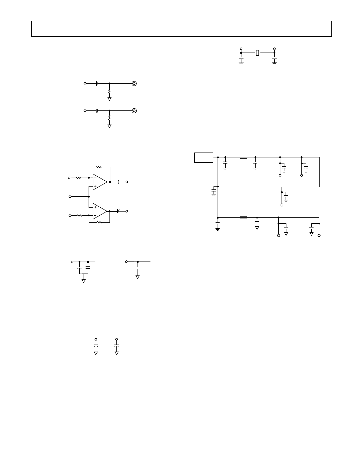
AD1845
Figure 30 shows ac-coupled line outputs. The resistors are used
to center the output signals around analog ground. If dc-coupling is desired, V
could be used with op amps as mentioned
REF
above, if desired.
L_OUT
R_OUT
1mF
47kV
1mF
47kV
Figure 30. Line Output Connections
A circuit for headphone drive is illustrated in Figure 31. Drive is
supplied by +5 V operational amps. The circuit shown ac
couples the headphones to the line output.
8.66kV
SSM-2135
8.66kV
470mF
470mF
HEADPHONE
LEFT
HEADPHONE
RIGHT
L_OUT
V_REF
R_OUT
10kV
10kV
Figure 31. Headphone Drive Connections
Figure 32 illustrates reference bypassing. V
should only be
REF_F
connected to its bypass capacitors.
XTAL1O
20–64pF
20–64pF
XTAL1I
24.576 MHz
Figure 34. Crystal Connections
Note: XTAL2I and XTAL2O, are not used in the AD1845.
Analog Devices also recommends a pull-down resistor for
PWRDWN.
Good, standard engineering practices should be applied for
power-supply decoupling. Decoupling capacitors should be
placed as close as possible to package pins. If a separate analog
power supply is not available, we recommend the circuit shown
in Figure 35 for using a single +5 V supply. Ferrite beads suffice
for the inductors shown (typically 600Ω at 100 MHz). This
circuitry should be as close to the supply pins as is practical.
+5V
SUPPLY
10mF
+
–
0.1mF
FB
FB
+
–
+
10mF
–
V
DD
V
DD
V
CC
0.1mF10mF
0.1mF
0.1mF
0.1mF
V
DD
0.1mF
0.1mF
V
CC
Figure 35. Recommended Power Supply Bypassing
V
REF_F
1.0µF
10µF
V
REF
10µF
Figure 32. Voltage Reference Bypassing
Figure 33 illustrates signal-path filtering capacitors, L_FILT
and R_FILT. The AD1845 must use 1.0 µF capacitors; the
AD1845 will not perform properly with 1000 pF capacitors.
The 1.0 µF capacitors required by the AD1845 can be of any
type.
L_FILT
1.0µF
R_FILT
1.0µF
Figure 33. External Filter Capacitor Connections
The crystal shown in the crystal connection circuitry of Figure 34 should be 24.576 MHz, fundamental-mode and paralleltuned. Note that using the exact data sheet frequencies is not
required and that external clock sources can be used to overdrive the AD1845’s internal oscillators. (See the description of
the CFS2:0 control bits above.) If using an external clock source,
apply it to the crystal input pins while leaving the crystal output
pins unconnected. Attention should be paid to providing low
jitter external input clocks.
GROUNDING AND LAYOUT
Analog Devices recommends a split ground plane as shown in
Figure 36. The analog plane and the digital plane are connected
directly under the AD1845. Splitting the ground plane directly
under the SoundPort Codec is optimal because analog pins will
be located above the analog ground plane and digital pins will
be located directly above the digital ground plane for the best
isolation.
Other schemes may also yield satisfactory results. If the split
ground plane recommended here is not possible, the AD1845
should be entirely over the analog ground plane with the optional 74_245 transceiver over the digital plane.
Some manufacturers of compatible devices differentiate between
digital supply pins used to power internal logic and digital supply pins used to power the ISA bus driver. Their recommended
layout suggests connecting the internal logic supply pins to the
analog supply. A potential problem can occur if the layout connects digital supply pins to the analog supply. Connecting some
of the digital supply pins to one supply and some of the digital
supply pins to a different supply can create an internal short
between the two different +5 V supplies.
REV. C
–35–
Page 36

AD1845
Analog Devices recommends that all digital pins be driven from
the same supply. A common technique to achieve maximum
performance is to use a +5 V regulator to power the analog side
of the codec from the PCs +12 V supply line, while the standard
PC +5 V supply line powers the entire digital side of the codec.
The separate supplies provide noise isolation for the analog side
of the codec, and maximize performance of the AD1845.
DIGITAL
GROUND
PLANE
GNDD
AD1845
PLCC
GNDD
44
25
R_AUX2
43
26
R_FILT
ANALOG
GROUND
PLANE
DIGITAL
GROUND
PLANE
NC
AD1845
TQFP
NC
ANALOG
NC
51
25
R_FILT
GROUND
PLANE
52
24
Figure 36. Recommended Ground Plane
COMPATIBILITY WITH CS4231
1. The CS4231 requires a 1000 pF NPO type capacitor on
Pins 26 and 31. The AD1845 requires a 1 µF capacitor on
filter Pins 26 and 31. To achieve compatibility with the
AD1845, use pad spacing that will accommodate either
1000 pF NPO capacitors for the CS4231 and the CS4248
or the 1 µF capacitors for the AD1845.
2. The AD1845 requires the input antialiasing filters for the
ADCs (refer to Figures 27 and 28). The CS4231 can use
the same filters with no degradation in performance. For
compatibility it is suggested that the filters be added.
3. The CS4231 does not require the power pins (V
DD
) 24,
45, and 54, or the ground pins (GNDD) 25, and 44. It is
suggested that the appropriate power/ground pin connections be made. This will not affect the performance of the
CS4231.
4. The CS4231 does not provide software programmable
power-down modes.
5. The CS4231 does not have the ability to mix the MIC
input with the DAC output.
6. The CS4231 does not contain a Variable Sample Frequency Generator and cannot change sample rates “on the
fly.” The CS4231 and CS4248 require entering MCE to
change the sample rate. The AD1845 can change the
sample rate without entering MCE. The AD1845’s 50,000
selectable sample rates are not available on the CS4231.
The Variable Sample Frequency Generator reduces clicks
and pops encountered in many game applications.
7. The CS4231 requires two crystal inputs, 24.575 MHz and
16.9344 MHz. The AD1845 requires only one input of
24.576 MHz or can be driven from OSC or other external clocks.
8. The CS4231 does not contain the INITD bit.
9. The CS4231 minimum R
= 20 kΩ. The AD1845 mini-
IN
mum input resistance is 10 kΩ.
10. The AD1845 does not include hardware for compressing
and decompressing ADPCM data. Analog Devices offers
Windows based software applets for using ADPCM formats with the AD1845.
–36–
REV. C
Page 37

FREQUENCY RESPONSE PLOTS
dB
SAMPLE FREQUENCY – F
S
10
–120
–90
–110
–100
–60
–80
–70
–50
–30
–20
0
–10
–40
0.700.40 0.64 0.680.600.560.520.480.44
AD1845
10
0
–10
–20
–30
–40
–50
dB
–60
–70
–80
–90
–100
–110
–120
0.0
0.1
SAMPLE FREQUENCY – F
0.8 0.90.70.60.50.40.30.2
S
1.0
Figure 37. Analog-to-Digital Frequency Response
(Full-Scale Line-Level Inputs, 0 dB)
to F
S
10
0
–10
–20
–30
–40
–50
dB
–60
–70
–80
–90
–100
–110
–120
0.40
SAMPLE FREQUENCY – F
0.64 0.680.600.560.520.480.44
S
0.70
Figure 38. Analog-to-Digital Frequency Response
—Transition Band (Full-Scale Line-Level Inputs, 0 dB)
10
0
–10
–20
–30
–40
–50
dB
–60
–70
–80
–90
–100
–110
–120
SAMPLE FREQUENCY – F
S
Figure 39. Digital-to-Analog Frequency
Response to F
(Full-Scale Inputs, 0 dB)
S
Figure 40. Digital-to-Analog Frequency Response
—Transition Band (Full-Scale Inputs, 0 dB)
1.00.10.0 0.8 0.90.70.60.50.40.30.2
REV. C
–37–
Page 38

AD1845
APPENDIX
EXTENDED TEMPERATURE SPECIFICATIONS
Test Conditions
The AD1845 has been tested over the industrial temperature range. The typical values represent the limits that change with temperature. All other limits remain unchanged.
Temperature –40°C to +85°C DAC Test Conditions
Digital Supply (V
Analog Supply (V
Sample Rate (F
Input Signal 1008 Hz Mute Off, OL = 0
Analog Output Passband 20 Hz to 20 kHz
V
IH
V
IL
V
OH
V
OL
Parameter Min Typ Max Units
Step Size (All Steps Tested) (0 dB to 22.5 dB) 1.75 dB
PGA Gain Range Span 22.83 dB
) 5.0 V Calibrated
DD
) 5.0 V 0 dB Attenuation
CC
) 48 kHz 16-Bit Linear Mode
S
2.0 V ADC Input Conditions
0.8 V Calibrated
2.4 V 0 dB Gain
0.4 V –1.0 dB Relative to Full Scale
Line Input
16-Bit Linear Mode
PROGRAMMABLE GAIN AMPLIFIER—ADC
AUXILIARY, LINE, MONO, AND MICROPHONE INPUT
ANALOG GAIN/AMPLIFIERS/ATTENUATORS
Parameter Min Typ Max Units
Step Size AUX1, AUX2, LINE, MIC (All Steps Tested):
(+12 dB to –34.5 dB, Referenced to DAC Full Scale) 1.5 dB
Step Size: M_IN (All Steps Tested) (0 dB to –45 dB) 3.0 dB
Input Gain/Attenuation Range: AUX1, AUX2, LINE, MIC 46.2 dB
Input Gain/Attenuation Range: M_IN 43.5 dB
ANALOG-TO-DIGITAL CONVERTERS
Parameter Min Typ Max Units
Dynamic Range (–60 dB Input THD+N Referenced to
Full Scale, A-Weighted) –81 dB
THD+N (Referenced to Full Scale) –76 dB
DIGITAL-TO -ANALOG CONVERTERS
Parameter Min Typ Max Units
Dynamic Range (–60 dB Input THD+N Referenced to
Full Scale, A-Weighted) –82 dB
THD+N (Referenced to Full Scale) –78 dB
DAC ATTENUATOR
Parameter Min Typ Max Units
Step Size (0 dB to –22.5 dB) –1.5 dB
ANALOG OUTPUT
Parameter Min Typ Max Units
V
REF
–38–
2.36 V
REV. C
Page 39

AD1845
TABLE OF CONTENTS
PRODUCT OVERVIEW . . . . . . . . . . . . . . . . . . . . . . . . . . . . . . 1
Expanded Mode (MODE2) . . . . . . . . . . . . . . . . . . . . . . . . . . . 9
SPECIFICATIONS . . . . . . . . . . . . . . . . . . . . . . . . . . . . . . . . . . 2
ORDERING GUIDE . . . . . . . . . . . . . . . . . . . . . . . . . . . . . . . . . 5
PIN DESIGNATIONS . . . . . . . . . . . . . . . . . . . . . . . . . . . . . . . . 6
PIN FUNCTION DESCRIPTIONS . . . . . . . . . . . . . . . . . . . . . 7
FUNCTIONAL DESCRIPTION . . . . . . . . . . . . . . . . . . . . . . . 10
Analog Inputs . . . . . . . . . . . . . . . . . . . . . . . . . . . . . . . . . . . . . 10
Analog Mixing . . . . . . . . . . . . . . . . . . . . . . . . . . . . . . . . . . . . 10
Analog-to-Digital Datapath . . . . . . . . . . . . . . . . . . . . . . . . . . 10
Digital-to-Analog Datapath . . . . . . . . . . . . . . . . . . . . . . . . . . 10
Digital Mixing . . . . . . . . . . . . . . . . . . . . . . . . . . . . . . . . . . . . 10
Analog Outputs . . . . . . . . . . . . . . . . . . . . . . . . . . . . . . . . . . . 10
Digital Data Types . . . . . . . . . . . . . . . . . . . . . . . . . . . . . . . . . 10
Timer Registers . . . . . . . . . . . . . . . . . . . . . . . . . . . . . . . . . . . 11
Interrupts . . . . . . . . . . . . . . . . . . . . . . . . . . . . . . . . . . . . . . . . 11
Power Supplies and Voltage Reference . . . . . . . . . . . . . . . . . 11
Clocks and Sample Rates . . . . . . . . . . . . . . . . . . . . . . . . . . . . 11
CONTROL REGISTERS . . . . . . . . . . . . . . . . . . . . . . . . . . . . . 11
Control Register Architecture . . . . . . . . . . . . . . . . . . . . . . . . 11
Direct Control Register Definitions . . . . . . . . . . . . . . . . . . . . 14
Index Address Register (ADR1:0 = 0) . . . . . . . . . . . . . . . . 14
Indexed Data Register (ADR1:0 = 1) . . . . . . . . . . . . . . . . . 14
Status Register (ADR1:0 = 2) . . . . . . . . . . . . . . . . . . . . . . 15
PIO Data Registers (ADR1:0 = 3) . . . . . . . . . . . . . . . . . . . 16
Indirect Control Register Definitions . . . . . . . . . . . . . . . . . . . 16
Left Input Control (IXA3:0 = 0) . . . . . . . . . . . . . . . . . . . . 16
Right Input Control (IXA3:0 = 1) . . . . . . . . . . . . . . . . . . . 16
Left Aux #1 Input Control (IXA3:0 = 2) . . . . . . . . . . . . . . 17
Right Aux #1 Input Control (IXA3:0 = 3) . . . . . . . . . . . . . 17
Left Aux #2 Input Control (IXA3:0 = 4) . . . . . . . . . . . . . . 17
Right Aux #2 Input Control (IXA3:0 = 5) . . . . . . . . . . . . . 17
Left DAC Control (IXA3:0 = 6) . . . . . . . . . . . . . . . . . . . . 18
Right DAC Control (IXA3:0 = 7) . . . . . . . . . . . . . . . . . . . 18
Clock and Data Format (IXA3:0 = 8) . . . . . . . . . . . . . . . . 19
Interface Configuration (IXA3:0 = 9) . . . . . . . . . . . . . . . . . 20
Pin Control (IXA3:0 = 10) . . . . . . . . . . . . . . . . . . . . . . . . . 20
Test and Initialization (IXA3:0 = 11) . . . . . . . . . . . . . . . . . 21
Miscellaneous Control (IXA3:0 = 12) . . . . . . . . . . . . . . . . 21
Digital Mix/Attenuation Control (IXA3:0 = 13) . . . . . . . . 22
DMA Playback Base Count . . . . . . . . . . . . . . . . . . . . . . . . 22
Upper Base Count (IXA3:0 = 14) . . . . . . . . . . . . . . . . . 22
Lower Base Count (IXA3:0 = 15) . . . . . . . . . . . . . . . . . . 23
Alternate Feature Enable /Left MIC Input Control
(IXA3:0 =16) . . . . . . . . . . . . . . . . . . . . . . . . . . . . . . . . . 23
MIC Mix Enable/Right MIC Input Control (IXA3:0 = 17) . 23
Left Line Gain, Attenuate, Mute, Mix (IXA3:0 = 18) . . . . 23
Right Line Gain, Attenuate, Mute, Mix (IXA3:0 = 19) . . . 24
Lower Timer Bits (IXA3:0 = 20) . . . . . . . . . . . . . . . . . . . . 24
Upper Timer Bits (IXA3:0 = 21) . . . . . . . . . . . . . . . . . . . . 25
Upper Frequency Select (IXA3:0 = 22) . . . . . . . . . . . . . . . 25
Lower Frequency Select (IXA3:0 = 23) . . . . . . . . . . . . . . . 25
Capture Playback Timer (IXA3:0 = 24) . . . . . . . . . . . . . . . 25
Revision ID (IXA3:0 = 25) . . . . . . . . . . . . . . . . . . . . . . . . . 26
Mono Control (IXA3:0 = 26) . . . . . . . . . . . . . . . . . . . . . . . 26
Power-Down Control (IXA3:0 = 27) . . . . . . . . . . . . . . . . . 27
Capture Data Format Control (IXA3:0 = 28) . . . . . . . . . . 27
Crystal, Clock Select/Total Power-Down (IXA3:0 = 29) . . 27
Capture Upper Base Count (IXA3:0 = 30) . . . . . . . . . . . . 28
Capture Lower Base Count (IXA3:0 = 31) . . . . . . . . . . . . 28
DATA AND CONTROL TRANSFERS . . . . . . . . . . . . . . . . . 29
Data Ordering . . . . . . . . . . . . . . . . . . . . . . . . . . . . . . . . . . . . 29
FIFO . . . . . . . . . . . . . . . . . . . . . . . . . . . . . . . . . . . . . . . . . . . 29
Data Bus Drivers . . . . . . . . . . . . . . . . . . . . . . . . . . . . . . . . . . 29
Control and Programmed I/O (PIO) Transfers . . . . . . . . . . . 29
DIRECT MEMORY ACCESS (DMA) TRANSFERS . . . . . . . 30
Single-Channel DMA . . . . . . . . . . . . . . . . . . . . . . . . . . . . . . 30
Dual-Channel DMA . . . . . . . . . . . . . . . . . . . . . . . . . . . . . . . 31
DMA Timing . . . . . . . . . . . . . . . . . . . . . . . . . . . . . . . . . . . . . 31
DMA Interrupt . . . . . . . . . . . . . . . . . . . . . . . . . . . . . . . . . . . 31
POWER-UP AND RESET . . . . . . . . . . . . . . . . . . . . . . . . . . . . 32
ADVANCED POWER-DOWN MODES . . . . . . . . . . . . . . . . . 32
AUTOCALIBRATION . . . . . . . . . . . . . . . . . . . . . . . . . . . . . . 33
CHANGING SAMPLE RATES . . . . . . . . . . . . . . . . . . . . . . . . 33
APPLICATIONS CIRCUITS . . . . . . . . . . . . . . . . . . . . . . . . . 34
GROUNDING AND LAYOUT . . . . . . . . . . . . . . . . . . . . . . . . 35
COMPATIBILITY WITH CS4231 . . . . . . . . . . . . . . . . . . . . . 36
FREQUENCY RESPONSE PLOTS . . . . . . . . . . . . . . . . . . . . 37
APPENDIX—EXTENDED TEMPERATURE
SPECIFICATIONS . . . . . . . . . . . . . . . . . . . . . . . . . . . . . . . . 38
PACKAGE OUTLINE DIMENSIONS . . . . . . . . . . . . . . . . . . 40
FIGURES TABLE OF CONTENTS
1. Interface to ISA Bus . . . . . . . . . . . . . . . . . . . . . . . . . . . . . . . 9
2. µ-Law or A-Law Expansion . . . . . . . . . . . . . . . . . . . . . . . . 11
3. µ-Law or A-Law Compression . . . . . . . . . . . . . . . . . . . . . . 11
4. Direct Register Map . . . . . . . . . . . . . . . . . . . . . . . . . . . . . . 11
5. Indirect Register Map and Reset/Default States . . . . . . . . . 12
6. Register Summary . . . . . . . . . . . . . . . . . . . . . . . . . . . . . . . . 13
7. Mix Gain Level Setting: DAC . . . . . . . . . . . . . . . . . . . . . . . 18
8. MODE1 Audio Sample Frequency Select . . . . . . . . . . . . . . 19
9. Digital Audio Data Type . . . . . . . . . . . . . . . . . . . . . . . . . . . 19
10. Mix Gain Level Setting: AUX1, AUX2, MIC, LINE . . . . . 24
11. Mono Attenuation . . . . . . . . . . . . . . . . . . . . . . . . . . . . . . . 26
12. Capture Audio Data Type . . . . . . . . . . . . . . . . . . . . . . . . . 27
13. Input Frequency Selection . . . . . . . . . . . . . . . . . . . . . . . . . 28
14. 8-Bit Mono Data Stream Sequencing . . . . . . . . . . . . . . . . . 29
15. 8-Bit Stereo Data Stream Sequencing . . . . . . . . . . . . . . . . . 29
16. 16-Bit Mono Data Stream Sequencing, Little Endian . . . . 29
17. 16-Bit Stereo Data Stream Sequencing, Little Endian . . . . 29
18. 16-Bit Mono Data Stream Sequencing, Big Endian . . . . . . 29
19. 16-Bit Stereo Data Stream Sequencing, Big Endian . . . . . . 29
20. Control Register/PIO Read Cycle . . . . . . . . . . . . . . . . . . . . 30
21. Control Register/PIO Write Cycle . . . . . . . . . . . . . . . . . . . 30
22. 8-Bit Mono DMA Read/Capture Cycle . . . . . . . . . . . . . . . 31
23. 8-Bit Mono DMA Write/Playback Cycle . . . . . . . . . . . . . . 31
24. 8-Bit Stereo or 16-Bit Mono DMA Cycle . . . . . . . . . . . . . . 31
25. 16-Bit Stereo DMA Interrupt . . . . . . . . . . . . . . . . . . . . . . . 31
26. Advanced Power-Down Mode Summary . . . . . . . . . . . . . . 32
27. 2 V rms Line-Level Input Circuit for LINE Inputs . . . . . . . 34
28. 2 V rms Line-Level Input Circuit for M_IN and
AUX Inputs . . . . . . . . . . . . . . . . . . . . . . . . . . . . . . . . . . . . 34
29. “Phantom Powered” Microphone Input Circuit . . . . . . . . . 34
30. Line Output Connections . . . . . . . . . . . . . . . . . . . . . . . . . . 35
31. Headphone Drive Connections . . . . . . . . . . . . . . . . . . . . . . 35
32. Voltage Reference Bypassing . . . . . . . . . . . . . . . . . . . . . . . . 35
33. External Filter Capacitor Connections . . . . . . . . . . . . . . . . 35
34. Crystal Connections . . . . . . . . . . . . . . . . . . . . . . . . . . . . . . 35
35. Recommended Power Supply Bypassing . . . . . . . . . . . . . . . 35
36. Recommended Ground Plane . . . . . . . . . . . . . . . . . . . . . . . 36
37. Analog-to-Digital Frequency Response to F
Line-Level Inputs, 0 dB) . . . . . . . . . . . . . . . . . . . . . . . . . . 37
38. Analog-to-Digital Frequency Response—Transition Band
(Full-Scale Line-Level Inputs, 0 dB) . . . . . . . . . . . . . . . . . 37
39. Digital-to-Analog Frequency Response to F
Inputs, 0 dB) . . . . . . . . . . . . . . . . . . . . . . . . . . . . . . . . . . . 37
40. Digital-to-Analog Frequency Response—Transition Band
(Full-Scale Inputs, 0 dB) . . . . . . . . . . . . . . . . . . . . . . . . . . 37
(Full-Scale
S
(Full-Scale
S
REV. C
–39–
Page 40
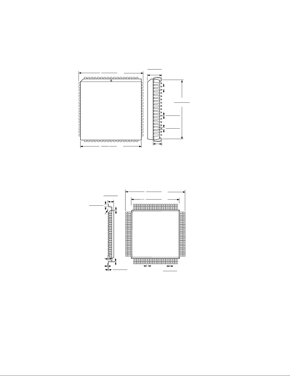
AD1845
OUTLINE DIMENSIONS
Dimensions shown in inches and (mm).
68-Lead Plastic Leaded Chip Carrier
(P-68A)
10
26
9
27
0.030 (0.75)
0.020 (0.50)
0.995 (25.27)
0.885 (22.48)
(PINS DOWN)
0.954 (24.23)
0.950 (24.13)
PIN 1
IDENTIFIER
TOP VIEW
SQ
SQ
61
60
44
43
100-Lead Thin Quad Flatpack
(ST-100)
0.057 (1.45)
0.053 (1.35)
100 76
12°
1
SEATING
PLANE
TYP
0.175 (4.45)
0.169 (4.29)
0.104 (2.64) TYP
0.640 (16.25)
0.620 (15.75)
0.553 (14.05)
0.549 (13.95)
0.050
(1.27)
TYP
0.019 (0.48)
0.017 (0.43)
0.029 (0.74)
0.027 (0.69)
SQ
SQ
0.925 (23.50)
0.895 (22.73)
75
0.004
(0.102)
MAX LEAD
COPLANARITY
0° – 7°
6° ± 4°
0.006 (0.15)
0.002 (0.05)
TOP VIEW
(PINS DOWN)
25
26
0.020 (0.50)
BSC
0.011 (0.27)
0.007 (0.17)
51
50
PRINTED IN U.S.A. C2008a–2–11/97
–40–
REV. C
 Loading...