

查询AD1317供应商查询AD1317供应商
Ultrahigh Speed
a
FEATURES
Full Window Comparator
2.0 pF max Input Capacitance
9 V max Differential Input Voltage
2.5 ns Propagation Delays
Low Dispersion
Low Input Bias Current
Independent Latch Function
Input Inhibit Mode
80 dB CMRR
APPLICATIONS
High Speed Pin Electronic Receiver
High Speed Triggers
Threshold Detectors
Peak Detectors
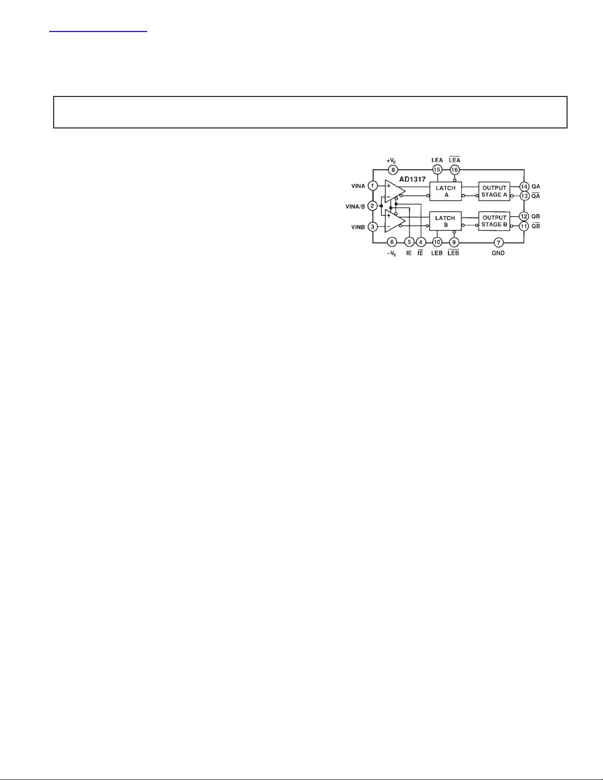
PRODUCT DESCRIPTION
The AD1317 is an ultrahigh speed window comparator with a
latch. It uses a high speed monolithic process to provide high dc
accuracy without sacrificing input voltage range. The AD1317
guarantees a 2.8 ns maximum propagation delay.
On-chip connection of the common input eliminates the contributions of a second bonding pad and package pin to the input
capacitance, resulting in a maximum input capacitance of 2 pF.
The dispersion, or variation in propagation delay with input
overdrive levels and slew rates, is typically 350 ps for 5 V signals
and 200 ps for 1 V inputs.
The AD1317 employs a high precision differential input stage
with a common-mode range of 9 V. Its complementary digital
Window Comparator with Latch
AD1317
FUNCTIONAL BLOCK DIAGRAM
outputs are ECL compatible. The output stage is capable of
driving a 50 Ω line terminated to –2 V. The AD1317 also pro-
vides a latch function, allowing operation in a sample-hold
mode. The latch inputs can also be used to generate hysteresis.
The comparator input can be switched into a high impedance
state through the inhibit mode feature, electrically removing the
comparator from the circuit. The bias current in inhibit mode is
typically 50 pA.
The AD1317 is available in a small 16-lead, hermetically sealed
“gull-wing” surface mount package and operates over the com-
mercial temperature range, 0°C to +70°C.
REV. A
Information furnished by Analog Devices is believed to be accurate and
reliable. However, no responsibility is assumed by Analog Devices for its
use, nor for any infringements of patents or other rights of third parties
which may result from its use. No license is granted by implication or
otherwise under any patent or patent rights of Analog Devices.
One Technology Way, P.O. Box 9106, Norwood, MA 02062-9106, U.S.A.
Tel: 617/329-4700 World Wide Web Site: http://www.analog.com
Fax: 617/326-8703 © Analog Devices, Inc., 1997

(All specifications at +258C, free air. Outputs terminated into 50 V to –2 V,
AD1317–SPECIFICATIONS
Parameter Symbol Min Typ Max Units Comments
DC INPUT CHARACTERISTICS
Offset Voltage V
Offset Drift dV
VINA/B Bias Currents –2 V to +7 V
Active Ibca 10 33 µA
Inhibit Ibci 50 pA
VINA, VINB Bias Currents –2 V to +7 V
Active Ibsa 5 16.5 µA
Inhibit Ibsi 50 pA
VINA/B Resistance Rinc 4 MΩ
VINA, VINB Resistance Rins 8 MΩ
Capacitance VINA/B, VINA, VINB C
Voltage Range V
Differential Voltage V
Common-Mode Rejection Ratio CMRR 70 80 dB –2 V to +7 V
LATCH ENABLE INPUTS
Input Voltage, Any Input –2.0 5.0 Volts
Differential Voltage 0.4 4 Volts
Logic “1” Current I
Logic “0” Current I
Capacitance 4 pF
INPUT ENABLE CURRENTS
Input Voltage, Any Input –2.0 5.0 Volts
Differential Voltage 0.4 4 Volts
Logic “1” Current I
Logic “0” Current I
Capacitance 4 pF
DIGITAL OUTPUTS
Logic “l” Voltage V
Logic “0” Voltage V
SWITCHING PERFORMANCE See Figure 3
Propagation Delays
Input to Output t
Latch Enable to Output t
Active to Inhibit t
Inhibit to Active t
Propagation Delay T.C. 5 ps/°C
Dispersion See Note 4
5 V Signal See Figure 1
All Edges 450 600 ps
Rising Edge 350 ps
Falling Edge 350 ps
1 V Signal See Figure 2
All Edges 250 400 ps
Rising Edge 200 ps
Falling Edge 200 ps
LATCH TIMING
Input Pulse Width t
Setup Time t
Hold Time t
POWER SUPPLIES
to +VS Range 15.2 15.6 See Note 5
–V
S
Positive Supply +V
Negative Supply –V
Positive Supply Current I+ 50 70 mA
Negative Supply Current I– –100 –70 mA
PSRR 65 75 dB Measured at ±2.5% of +V
NOTES
1
P
ropagation Delay is measured from the input threshold crossing at the 50% point of a 0 V to 5 V input to the output Q and Q crossing.
2
Propagation Delay is measured from the input crossing of IE and IE to when the input bias currents drop to 10% of their nominal value.
3
Propagation Delay is measured from the input crossing of IE and IE to when the input bias currents rise to 90% of their nominal value.
4
Dispersion is measured with input slew rates of 0.5 V/ns and 2.5 V/ns for 5 V swings, 0.5 V/ns and 1 V/ns for 1 V swings.
5
The comparator input voltage range is specified for –2 V to +7 V for typical power supply values of -5.2 V and +10.0 V but can be offset for different input ranges such as –1 V to
+8 V with power supplies of –4.2 V and +11 V, as long as the required headroom of 3 V is maintained between both V
Specifications subject to change without notice.
OS
/dT 20 µV/°C
OS
IN
CM
DIFF
IH
IL
IH
IL
OH
OL
, t
PDR
LO
IN
IE
PW
S
H
S
S
with + VS = +10 V, –VS = 5.2 V unless otherwise noted)
AD1317KZ
–10 10 mV CMV = 0 V
–2 7 Volts See Note 5
–200 µA
–200 µA
–0.98 Volts
PDF
2.5 1.0 ns
1.5 0.4 ns
0ns
8.0 10.0 11.0 Volts
–7.2 –5.2 –4.2 Volts
1.5 2.0 pF
9 Volts
10 µA
20 µA
–1.50 Volts
1.8 2.8 ns See Note 1
2.0 2.5 ns See Note 1
2.5 ns See Note 2
15 ns See Note 3
and +VS and VL and +VS.
H
and –V
S
S
–2–
REV. A
AD1317
WARNING!
ESD SENSITIVE DEVICE
ABSOLUTE MAXIMUM RATINGS
1
Power Supply Voltage
+V
to GND . . . . . . . . . . . . . . . . . . . . . . . . . . . . . . . +12 V
S
–V
to GND . . . . . . . . . . . . . . . . . . . . . . . . . . . . . . . . . –9 V
S
Difference from +V
to –VS . . . . . . . . . . . . . . . . . . . . +16 V
S
Inputs
VINA/B, VINA, VINB . . . . . . . +V
LEA, LEA, LEB, LEB . . . . . . . . . . +V
IE, IE . . . . . . . . . . . . . . . . . . . . . . +V
Outputs
2
– 13.5 V, –VS + 13.7 V
S
– 14 V, –VS + 12 V
S
– 14 V, –VS + 10.3 V
S
QA, QA, QB, QB . . . . . . . . . . GND – 0.5 V, GND + 3.5 V
Operating Temperature Range . . . . . . . . . . . . . 0°C to +70°C
Storage Temperature Range
After Soldering . . . . . . . . . . . . . . . . . . . . . –65°C to + 125°C
Lead Temperature Range (Soldering 20 sec)
NOTES
1
Stresses above those limits under Absolute Maximum Ratings may cause permanent damage to the device. This is a stress rating only; functional operation of the
device at these or any other conditions above those indicated in the operational
sections of this specification is not implied. Exposure to absolute maximum rating
conditions for extended periods may affect device reliability.
2
Limits apply for shorted output.
3
To ensure lead coplanarity (±0.002 inches) and solderability, handling with bare
hands should be avoided and the device should be stored in an environment at
24°C ± 5°C (75°F ±10°F) with relative humidity not to exceed 65%.
3
. . . . . . .+300°C
ORDERING GUIDE
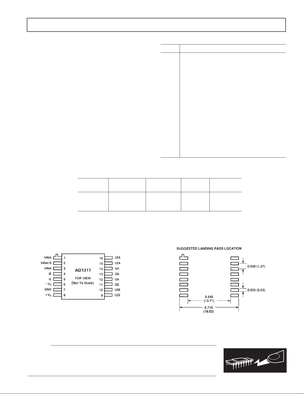
WINDOW COMPARATOR PIN ASSIGNMENT
Pin No. Description
1 VINA Noninverting Comparator A Input
2 VINA/B Window Comparator Common Input
3 VINB Inverting Comparator B Input
4 IE Input Enable
5 IE Input Enable
6–V
S
Negative Supply, –5.2V
7 GND Ground
8+V
S
Positive Supply, +10 V
9 LEB Latch Enable B
10 LEB Latch Enable B
11 QB Comparator B Output
12 QB Comparator B Output
13 QA Comparator A Output
14 QA Comparator A Output
15 LEA Latch Enable A
16 LEA Latch Enable A
Temperature Package
Model Range Description Option* Quantity
AD1317KZ 0°C to +70°C 16-Lead Z-16A 1-24
Gull Wing 25–99
100+
*Z = Ceramic Leaded Chip Carrier.
CONNECTION DIAGRAMS
Dimensions shown in inches and (mm).
CAUTION
ESD (electrostatic discharge) sensitive device. Electrostatic charges as high as 4000 V readily
accumulate on the human body and test equipment and can discharge without detection.
Although the AD1317 features proprietary ESD protection circuitry, permanent damage may
occur on devices subjected to high energy electrostatic discharges. Therefore, proper ESD
precautions are recommended to avoid performance degradation or loss of functionality.
–3–REV. A

AD1317
DEFINITION OF TERMS
Vos INPUT OFFSET VOLTAGE—The voltage that
must be applied between either VINA and VINA/B or
VINB and VINA/B to obtain zero voltage between
outputs QA and QA, or QB and QB, respectively.
dV
/dT OFFSET DRIFT—The ratio of the change in input
OS
offset voltages, over the operating temperature range,
to the change in temperature.
Ibca INPUT BIAS CURRENT (VINA/B, ACTIVE)—
The bias current of the window comparator’s common input with inputs enabled.
Ibci INPUT BIAS CURRENT (VINA/B, INHIBIT)—
The bias current of the window comparator’s common input with inputs inhibited.
Ibsa INPUT BIAS CURRENT (VINA or VINB,
ACTIVE)—The bias current of either single input
with inputs active.
Ibsi INPUT BIAS CURRENT (VINA or VINB,
INHIBIT)—The bias current of either single input
with inputs inhibited.
Rinc INPUT RESISTANCE (VINA/B)—The input
resistance looking into the window comparator’s
common input.
Rins INPUT RESISTANCE (VINA or VINB)—The
input resistance looking into either single input.
C
IN
INPUT CAPACITANCE (VINA/B)—The capacitance looking into the window comparator’s common
input.
V
CM
INPUT COMMON-MODE VOLTAGE RANGE—
The range of voltages on the input terminals for
which the offset and propagation delay specifications
apply.
V
DIFF
INPUT DIFFERENTIAL VOLTAGE RANGE—
The maximum difference between any input terminal
voltages.
CMRR COMMON-MODE REJECTION RATIO—The
ratio of common-mode input voltage range to the
peak-to-peak change in input offset voltage over this
range.
I
IH
LOGIC “1” INPUT CURRENT—The logic high
current flowing into (+) or out of (–) a logic input.
I
IL
LOGIC “0” INPUT CURRENT—The logic low
current flowing into (+) or out of (–) a logic input.
V
OH
LOGIC “1” OUTPUT VOLTAGE—The logic high
output voltage with a specified load.
V
OL
LOGIC “0” OUTPUT VOLTAGE—The logic low
output voltage with a specified load.
I
OH
LOGIC “1” OUTPUT CURRENT—The logic high
output source current.
I
OL
LOGIC “0” OUTPUT CURRENT—The logic low
output source current.
I+ POSITIVE SUPPLY CURRENT—The current
required from the +V
supply.
S
I– NEGATIVE SUPPLY CURRENT—The current
required from the –V
supply.
S
PSRR POWER SUPPLY REJECTION RATIO—The ratio
of power supply voltage change to the peak-to-peak
change in input offset voltage.
AD1317 SWITCHING TERMS (See Figure 3)
t
PDR
INPUT TO OUTPUT RISING EDGE DELAY—
The propagation delay measured from the time
VINA/B crosses either VINA or VINB, in a low to
hi
gh transition, to the time QA and QA or QB and
QB cross, respectively.
t
PDF
INPUT TO OUTPUT FALLING EDGE DELAY—
The propagation delay measured from the time
VINA/B crosses either VINA or VINB, in a high to
low transition, to the time QA and QA or QB and
QB cross, respectively.
t
S
MINIMUM LATCH SET-UP TIME—The minium
time before LE goes high with respect to LE that an
input signal change must be present in order to be
acquired and held at the outputs.
t
H
MINIMUM LATCH HOLD TIME—The minium
time after LE goes high with respect to LE that the
input signal must remain unchanged in order to be
acquired and held at the outputs.
t
PW
MINIMUM LATCH ENABLE PULSE WIDTH—
The minimum time that LE must be held high with
respect to LE in order to acquire and hold an input
change.
t
LO
LATCH ENABLE TO OUTPUT DELAY—The
time between when LE goes high with respect to LE
that QA and QA or QB and QB cross.
t
ID
INPUT STAGE DISABLE TIME—The time between when IE goes high with respect to IE that the
input bias currents drop to 10% of their nominal
value.
t
IE
INPUT STAGE ENABLE TIME—The time between when IE goes high with respect to IE that the
input bias currents rise to 90% of their nominal values.
–4–
REV. A

Figure 1. Dispersion Test Input Conditions—5 V Signal
AD1317
Figure 2. Dispersion Test Input Conditions—1 V Signal
Figure 3. Timing Diagram
–5–REV. A

AD1317
—Typical Performance Characteristics
Figure 4. Response to Overdrive Variation—Rising Edge
Figure 5. Response to Various Signal Levels—Rising Edge
Figure 7. Response to Overdrive Variation—Falling Edge
Figure 8. Response to Various Signal Levels—Falling
Edge
Figure 6. Propagation Delay vs. Slew Rate
Figure 9. Propagation Delay vs. Temperature—Rising
Edge
–6–
REV. A

AD1317
Figure 10. Propagation Delay
vs. Temperature—Falling Edge
Figure 13. Voltage Gain vs. Frequency
Figure 11. Output Waveform vs. Load Figure 12. Propagation Delay vs.
Common-Mode Voltage
Figure 16. Common-Mode Range vs. Power Supply
Figure 14. Output Levels vs. Temperature
Figure 15. Input Bias Current vs. Input Voltage
Figure 17. Input Bias Current vs. Temperature
Figure 18. Input Bias Current vs. Input Voltage
–7–REV. A

AD1317
—Typical Performance Characteristics
Figure 19. Change in Bias Current vs. Input Differential
Voltage (VINA/B – VINA, VINB)
Figure 20. Power Supply Currents vs. Temperature
Figure 22. Output Voltage vs. Source Current
Figure 23. Inhibit Input Bias Current vs. Common-Mode
Voltage
Figure 21. Inhibit Input Bias Current vs. Input Voltage
(VINA/B = 7 V)
Figure 24. Inhibit Input Bias Current vs. Input Voltage
(VINA/B = –2 V)
–8–
REV. A

FUNCTIONAL DESCRIPTION
The AD1317 is an ultrahigh speed window comparator designed
for use in general purpose instrumentation and automatic test
equipment. The internal connections for windowing operation
keep the capacitance at the critical common input (VINA/B)
well below what could normally be obtained using separate input
pins.
Another key feature is that the front end circuitry may be disabled, decreasing input bias currents to 50 pA (typical). This
enables sensitive dc current testing without having to physically
disconnect the AD1317’s input from the circuit. The comparator’s
outputs would normally be latched to maintain absolute logic
levels prior to inhibiting the input.
High speed comparators using bipolar process technology usu-
ally have input bias currents in the 1 µA to 20 µA range, and the
AD1317 is no exception in this regard. This occurs because the
input devices usually have low current gain but must be operated at high currents to obtain the widest possible bandwidth.
Careful design minimizes variations in the AD1317’s bias current with respect to both differential and common-mode input
variations. This translates directly to a high equivalent input
resistance, the minimum of which occurs with zero differential
input. The typical input resistance of the AD1317’s common
input under this condition is on the order of 4 megohms.
Many ATE applications have required input dividers/buffers to
reduce standard logic voltages to levels which can be processed
by “687” type comparators. These dividers have also reduced
the slew rates at which the comparators must properly function.
The AD1317’s 9 volt differential and common-mode input
ranges and 2.5 V/ns slew rate capability make these buffer circuits unnecessary in most applications.
Separate, complementary latch inputs are provided for each
comparator. These may be driven by differential or single-ended
sources ranging from ECL to HCMOS logic. When using the
comparator’s transparent mode, the latch inputs may be tied
anywhere within their common-mode range with a maximum
differential of 4 V. Symmetrical hysteresis may also be generated
by applying a small differential voltage to the latch inputs (see
HYSTERESIS).
The AD1317’s outputs are standard emitter followers with ECLcompatible voltage swings. The recommended output termina-
tion is 50 Ω to –2 V. Larger value termination resistors connected
to –V
may be used, but will reduce edge fidelity. Typical
S
output rise and fall times (20%–80%) are 1 ns with a 50 Ω,
10 pF load. The maximum output source current is 40 mA.
AD1317
Figure 25. Case-to-Ambient Thermal Resistance vs. Air
Flow
DISPERSION
Propagation delay dispersion is the change in device propagation
delay which results from changes in the input signal conditions.
Dispersion is an indicator of how well the comparator’s frontend
design balances the conflicting requirements of high gain and
wide bandwidth. High gain is needed to ensure that small overdrives will produce valid logic outputs without an increase in
propagation delay, while wide bandwidth enables the comparator to handle fast input slew rates. The input signal criteria used
to determine the AD1317’s dispersion performance are amplitude, overdrive and slew rate for both standard CMOS and
ECL signal levels.
HYSTERESIS
The customary technique for introducing hysteresis into a comparator uses positive feedback as shown in Figure 27. The major
problems with this approach are that the amount of hysteresis
varies with the output logic levels and that the hysteresis is not
symmetrical around zero.
The AD1317 does not use this technique. Instead, hysteresis is
generated by introducing a differential voltage between LE and
LE as shown in Figure 28. Hysteresis generated in this manner
is independent of output swing and is symmetrical around zero.
The variation of hysteresis with input voltage is shown in Figure
29; the useful hysteresis range is about 20 mV.
THERMAL CONSIDERATIONS
The AD1317 is provided in a 0.450" × 0.450", 16-lead (bottom
brazed) gull wing, surface mount package with a typical θ
JC
(junction-to-case thermal resistance) of 17.5°C/W. Thermal
resistance θ
this package is shown in Figure 25. The improvement in thermal
resistance vs. air flow begins to flatten out just above 400 lfm
NOTES
1
lfm is airflow in linear feet/minute.
2
For convection cooled systems, the minimum recommended airflow is 400 lfm.
(case to ambient) vs. air flow for the AD1317 in
CA
1, 2
.
–9–REV. A
LAYOUT CONSIDERATIONS
Like any high speed device, the AD1317 requires careful layout
and bypassing to obtain optimum performance. Oscillations are
generally caused by coupling from an output to the high impedance inputs. All drive impedances should be as low as possible,
and lead lengths should be minimized. A ground plane should
be used to provide low impedance return paths. Care should be
taken in selecting sockets for incoming or other testing to minimize lead inductance, and sockets are not recommended for
production use.

AD1317
Output wire lengths should be kept below one inch. Longer
connections require the use of transmission line techniques to
prevent ringing and reflections. Lines should be terminated with
their characteristic impedance to –2 V. Thevenin-equivalent
termination to –V
High quality RF capacitors should be used for power supply
bypassing. These should be located as closely as possible to the
AD1317’s power pins and connections to the ground plane
should have the minimum possible length. Both +V
must be bypassed with 470 pF capacitors located within 0.25
inches of the device’s supply pins. In addition, each supply
should be bypassed with 0.1 µF ceramic and 10 µF tantalum
capacitors. Low impedance power distribution techniques will
make the locations of these components less critical. Adding
470 pF capacitors at the VINA and VINB inputs, as close as
possible to the package, will improve circuit performance and
noise immunity in dc-compare applications.
is also possible.
S
and –V
S
S
Figure 28. Comparator Hysteresis Test Setup
Figure 26. Basic Circuit Decoupling
Figure 27. Typical Comparator Hysteresis
Figure 29. Typical Hysteresis Curve
Figure 30. Hysteresis
–10–
REV. A

AD1317
Figure 31. High Speed Digital Test System Block Diagram
–11–REV. A

AD1317
OUTLINE DIMENSIONS
Dimensions shown in inches and (mm).
Ceramic Leaded Chip Carrier
(Z-16A)
C1414a–0–6/97
–12–
PRINTED IN U.S.A.
REV. A
 Loading...