

Page 1

www.BDTIC.com/ADI
12-Bit, 400 MSPS A/D Converter
FEATURES
Up to 400 MSPS sample rate
SNR of 63 dBFS @128 MHz
SFDR of 70 dBFS @128 MHz
VSWR of 1:1.5
High or low gain grades
Wideband ac-coupled input signal conditioning
Enhanced spurious-free dynamic range
Single-ended or differential ENCODE signal
LVDS output levels
Twos complement output data
APPLICATIONS
Communications test equipment
Radar and satellite subsystems
Phased array antennas, digital beams
Multichannel, multimode receivers
Secure communications
Wireless and wired broadband communications
Wideband carrier frequency systems
GENERAL DESCRIPTION
The AD12401 is a 12-bit analog-to-digital converter (ADC)
with a transformer-coupled analog input and digital postprocessing for enhanced SFDR. The product operates at up to
400 MSPS conversion rate with outstanding dynamic performance
in wideband carrier systems.
The AD12401 requires a 3.7 V analog supply and 3.3 V and
1.5 V dig
that can be differential or single ended. No external reference is
required.
The AD12401 package style is an enclosed 2.9" × 2.6" × 0.6"
m
temperature range.
ital supplies, and provides a flexible ENCODE signal
odule. Performance is rated over a 0°C to 60°C case
AD12401
FUNCTIONAL BLOCK DIAGRAM
AD12401
ADC
A
POST-
A
IN
CLK DISTRIBUTION
ADC
B
CLOCK DISTRIBUTION
DIVIDE BY 2
ENC ENC
Figure 1.
PRODUCT HIGHLIGHTS
1. Guaranteed sample rate up to 400 MSPS.
2. I
nput signal conditioning with optimized dynamic
performance to 175 MHz.
3. H
igh and low gain grades available.
4. A
dditional performance options available (sample rates
>400 MSPS or second Nyquist zone operation); contact
sales.
5. Propr
ietary Advanced Filter Bank (AFB™) digital post-
processing from V Corp Technologies, Inc.
PROCESSING
OROUT
DATA
READY
A
DA0–DA11
DB0–DB11
DR_EN
DATA
READY
B
005649-001
Rev. A
Information furnished by Analog Devices is believed to be accurate and reliable. However, no
responsibility is assumed by Anal og Devices for its use, nor for any infringements of patents or ot her
rights of third parties that may result from its use. Specifications subject to change without notice. No
license is granted by implication or otherwise under any patent or patent rights of Analog Devices.
Trademarks and registered trademarks are the property of their respective owners.
One Technology Way, P.O. Box 9106, Norwood, MA 02062-9106, U.S.A.
Tel: 781.329.4700 www.analog.com
Fax: 781.461.3113 ©2006 Analog Devices, Inc. All rights reserved.
Page 2

AD12401
www.BDTIC.com/ADI
TABLE OF CONTENTS
Features .............................................................................................. 1
Time-Interleaving ADCs........................................................... 18
Applications....................................................................................... 1
Functional Block Diagram .............................................................. 1
General Description......................................................................... 1
Product Highlights........................................................................... 1
Revision History ............................................................................... 2
Specifications..................................................................................... 3
DC Specifications ......................................................................... 3
AC Specifications—ENCODE = 400 MSPS.............................. 4
AC Specifications—ENCODE = 360 MSPS.............................. 5
AC Specifications—ENCODE = 326 MSPS.............................. 6
Absolute Maximum Ratings............................................................ 8
Explanation of Test Levels........................................................... 8
ESD Caution.................................................................................. 8
Pin Configuration and Function Descriptions........................... 10
Te r mi n ol o g y .................................................................................... 13
Analog Input............................................................................... 18
Clock Input.................................................................................. 18
Digital Outputs........................................................................... 19
Power Supplies ............................................................................ 19
Start-Up and
DR_EN......................................................................................... 19
Overrange.................................................................................... 19
Gain Select................................................................................... 20
Thermal Considerations............................................................ 20
Package Integrity/Mounting Guidelines ................................. 20
AD12401 Evaluation Kit ........................................................... 21
Data Outputs............................................................................... 21
Layout Guidelines........................................................................... 26
PCB Interface.............................................................................. 26
Outline Dimensions ....................................................................... 28
RESET
.................................................................. 19
Typical Performance Characteristics........................................... 15
Theory of Operation ...................................................................... 18
REVISION HISTORY
4/06—Rev. 0 to Rev. A
Changes to Features and Product Highlights ............................... 1
Changes to Table 1............................................................................ 3
Changes to Table 2............................................................................ 4
Changes to Table 4............................................................................ 6
Changes to Table 7............................................................................ 9
Changes to Figure 5........................................................................ 10
Changes to Table 9.......................................................................... 11
Added Gain Select Section ............................................................ 20
Added H/L_GAIN Section............................................................ 21
Changes to Figure 25...................................................................... 23
Changes to the Ordering Guide.................................................... 28
7/05—Revision 0: Initial Version
Ordering Guide .......................................................................... 28
Rev. A | Page 2 of 28
Page 3

AD12401
www.BDTIC.com/ADI
SPECIFICATIONS
DC SPECIFICATIONS
VA = 3.7 V, VC = 3.3 V, VD = 1.5 V, 0°C ≤ T
Table 1.
AD12401-xxxKWS AD12401-xxxJWS
Parameter Case Temp Test Level Min Typ Max Min Typ Max Unit
RESOLUTION 12 Bits
ACCURACY
No Missing Codes Full IV Guaranteed
Offset Error Full I −12 +12 −12 +12 LSB
Gain Error @ 10 MHz Full I −10 +10 −10 +10 %FS
Differential Nonlinearity (DNL) 60°C V ±0.3 ±0.3 LSB
Integral Nonlinearity (INL) 60°C V ±0.5 ±0.5 LSB
TEMPERATURE DRIFT
Gain Error 60°C V 0.02 0.02 %/°C
ANALOG INPUT (AIN)
Full-Scale Input Voltage Range 60°C V 3.2 1.6 V p-p
Flatness (10 MHz to 175 MHz) Full IV 0.5 1 0.5 1 dB
Input VSWR, 50 Ω (300 kHz to 175 MHz) 60°C V 1.5 1.5
Analog Input Bandwidth 60°C V 480 480 MHz
POWER SUPPLY
Supply Voltage
VA Full IV 3.6 3.8 3.6 3.8 V
VC Full IV 3.2 3.4 3.2 3.4 V
VD Full IV 1.45 1.55 1.45 1.55 V
Supply Current
IVA (VA = 3.7 V) Full I 0.95 1.2 0.95 1.2 A
IVC (VC = 3.3 V) Full I 400 500 400 500 mA
IVD (VD = 1.5 V) Full I 0.8 1.2 0.8 1.2 A
Total Power Dissipation Full I 5.7 6.8 5.7 6.8 W
ENCODE INPUTS
Differential Inputs (ENC, ENC)
Input Voltage Full IV 0.4 0.4 V
Input Resistance 60°C V 100 100 Ω
Input Capacitance 60°C V 35 35 pF
Common-Mode Voltage 60°C V ±3 ±3 V
Single-Ended Inputs (ENC)
Input Voltage Full IV 0.4 2 0.4 2 V p-p
Input Resistance 60°C V 50 50 Ω
LOGIC INPUTS (RESET)
Logic 1 Voltage Full IV 2.0 2.0 V
Logic 0 Voltage Full IV 0.8 0.8 V
Source I
Sink I
LOGIC INPUTS (DR_EN)
Logic 1 Voltage Full IV 1.7 1.7 V
Logic 0 Voltage Full IV 0.7 0.7 V
Source I
Sink I
1
2
IH
IL
IH
IL
≤ 60°C, unless otherwise noted.
CASE
60°C IV 3.4 6 3.4 6 mA
60°C IV 0.9 1 0.9 1 mA
60°C IV 20 50 20 50 μA
60°C IV 30 160 30 160 μA
Rev. A | Page 3 of 28
Page 4

AD12401
www.BDTIC.com/ADI
AD12401-xxxKWS AD12401-xxxJWS
Parameter Case Temp Test Level Min Typ Max Min Typ Max Unit
LOGIC OUTPUTS (DRA, DRB, OUTPUT BITS)
Differential Output Voltage Full IV 247 350 454 247 350 454 mV
Output Common-Mode Voltage Full IV 1.125 1.25 1.375 1.125 1.25 1.375 V
Output High Voltage 60°C IV 1.602 1.602 V
Output Low Voltage 60°C IV 0.898 0.898 V
1
Tested using input frequency of 70 MHz (see Figure 17).
2
Refer to Table 8 for logic convention on all logic inputs.
3
Digital output logic levels: VC = 3.3 V, C
LOAD
AC SPECIFICATIONS1—ENCODE = 400 MSPS
VA = 3.7 V, VC = 3.3 V, VD = 1.5 V, ENCODE = 400 MSPS, 0°C ≤ T
Table 2.
AD12401-400KWS AD12401-400JWS
Parameter Case Temp Test Level Min Typ Max Min Typ Max Unit
DYNAMIC PERFORMANCE
SNR
Analog Input 10 MHz Full I 62 64 60 62 dBFS
@ −1.0 dBFS 70 MHz Full I 61.5 63.5 59.5 61.5 dBFS
128 MHz Full I 60 63 58 61 dBFS
2
SINAD
Analog Input 10 MHz Full I 59 63.5 57 61.5 dBFS
@ −1.0 dBFS 70 MHz Full I 58.5 63 56.5 61 dBFS
Spurious-Free Dynamic Range
Analog Input 10 MHz Full I 69 85 69 85 dBFS
@ −1.0 dBFS 70 MHz Full I 69 80 69 80 dBFS
Image Spur
Analog Input 10 MHz Full I 60 75 60 75 dBFS
@ −1.0 dBFS 70 MHz Full I 60 72 60 72 dBFS
Offset Spur
Analog Input @ −1.0 dBFS 60°C V 65 65 dBFS
Two-Tone IMD
F1, F2 @ −6 dBFS 60°C V −75 −75 dBc
ANALOG INPUT
Frequency Range Full IV 10 175 10 175 MHz
DIGITAL INPUT (DR_EN)
Minimum Time (Low) Full IV 5.0 5.0 ns
SWITCHING SPECIFICATIONS
Conversion Rate
Encode Pulse Width High (tEH)
Encode Pulse Width Low (tEL)
175 MHz Full I 60 62.5 57.5 60.5 dBFS
128 MHz Full I 57.5 61.5 55.5 59.5 dBFS
175 MHz Full I 55 60 53 58 dBFS
3
128 MHz Full I 66 72 66 72 dBFS
175 MHz Full I 62 68 62 68 dBFS
4
128 MHz Full I 60 66 60 66 dBFS
175 MHz Full I 57 63 57 63 dBFS
4
5
6
1
1
3
= 8 pF, 2.5 V LVDS, RT = 100 Ω.
Full IV 396 400 404 396 400 404 MSPS
60°C V 1.25 1.25 ns
60°C V 1.25 1.25 ns
≤ 60°C, unless otherwise noted.
CASE
Rev. A | Page 4 of 28
Page 5

AD12401
www.BDTIC.com/ADI
AD12401-400KWS AD12401-400JWS
Parameter Case Temp Test Level Min Typ Max Min Typ Max Unit
DIGITAL OUTPUT PARAMETERS
Valid Time (tV) Full IV 3.9 3.9 ns
Propagation Delay (tPD) 60°C V 8.7 8.7 ns
Rise Time, tR (20% to 80%) 60°C V 0.3 0.3 ns
Fall Time, tF (20% to 80%) 60°C V 0.3 0.3 ns
DR Propagation Delay (t
Data to DR Skew (t
Pipeline Latency
7
Start-Up Time Full IV 29 44 87 29 44 87 ms
Postprocessing Configuration Time Full IV 2.8 2.8 sec
APERTURE DELAY (tA) 60°C V 2.3 2.3 ns
APERTURE UNCERTAINTY (Jitter, tJ) 60°C V 0.4 0.4 ps rms
1
All ac specifications tested with a single-ended, 2.0 V p-p encode on ENCODE and
2
The image spur is included in the SINAD measurement.
3
The image spur is not included in the SFDR specification.
4
The image spur is at fS/2 – AIN; the offset spur is at fS/2.
5
F1 = 70 MHz, F2 = 73 MHz.
6
Parts are tested with 400 MSPS encode. Device can be clocked at lower encode rates, but specifications are not guaranteed. Specifications are guaranteed by design
for encode 400 MSPS ± 1%.
7
Pipeline latency is exactly 74 cycles with an additional tPD required for data to emerge.
) 60°C V 11.2 11.2 ns
EDR
− tPD) 60°C V 2.5 2.5 ns
EDR
Full IV 74 74 Cycles
ENCODE
floating.
AC SPECIFICATIONS1—ENCODE = 360 MSPS
VA = 3.7 V, VC = 3.3 V, VD = 1.5 V, encode = 360 MSPS, 0°C ≤ T
Table 3.
AD12401-360KWS
Parameter Case Temp Test Level Min Typ Max Unit
DYNAMIC PERFORMANCE
SNR
Analog Input 10 MHz Full I 62 64 dBFS
@ −1.0 dBFS 70 MHz Full I 61.5 63.5 dBFS
128 MHz Full I 60 63 dBFS
2
SINAD
Analog Input 10 MHz Full I 59 63.5 dBFS
@ −1.0 dBFS 70 MHz Full I 58.5 63 dBFS
128 MHz Full I 57.5 61.5 dBFS
Spurious-Free Dynamic Range
3
Analog Input 10 MHz Full I 69 85 dBFS
@ −1.0 dBFS 70 MHz Full I 69 80 dBFS
128 MHz Full I 66 72 dBFS
Image Spur
4
Analog Input 10 MHz Full I 60 75 dBFS
@ −1.0 dBFS 70 MHz Full I 60 72 dBFS
128 MHz Full I 60 66 dBFS
Offset Spur
4
Analog Input @ −1.0 dBFS 60°C V 65 dBFS
Two-Tone IMD
5
F1, F2 @ −6 dBFS 60°C V −75 dBc
ANALOG INPUT
Frequency Range Full IV 10 160 MHz
DIGITAL INPUT (DR_EN)
Minimum Time (Low) Full IV 5.6 ns
≤ 60°C, unless otherwise noted.
CASE
Rev. A | Page 5 of 28
Page 6

AD12401
www.BDTIC.com/ADI
AD12401-360KWS
Parameter Case Temp Test Level Min Typ Max Unit
SWITCHING SPECIFICATIONS
Conversion Rate
Encode Pulse Width High (tEH)
Encode Pulse Width Low (tEL)
DIGITAL OUTPUT PARAMETERS
Valid Time (tV) Full IV 4.5 ns
Propagation Delay (tPD) 60°C V 8.7 ns
Rise Time, tR (20% to 80%) 60°C V 0.3 ns
Fall Time, tF (20% to 80%) 60°C V 0.3 ns
DR Propagation Delay (t
Data to DR Skew (t
Pipeline Latency
Start-Up Time Full IV 29 44 87 ms
Postprocessing Configuration Time Full IV 3.1 sec
APERTURE DELAY (tA) 60°C V 2.3 ns
APERTURE UNCERTAINTY (Jitter, tJ) 60°C V 0.4 ps rms
1
All ac specifications tested with a single-ended, 2.0 V p-p encode on ENCODE and
2
The image spur is included in the SINAD specification.
3
The image spur is not included in the SFDR specification.
4
The image spur is at fS/2 – AIN; the offset spur is at fS/2.
5
F1 = 70 MHz, F2 = 73 MHz.
6
Parts are tested with 360 MSPS encode. Device can be clocked at lower encode rates, but specifications are not guaranteed. Specifications are guaranteed by design
for encode 360 MSPS ± 1%.
7
Pipeline latency is exactly 74 cycles with an additional tPD required for data to emerge.
6
1
1
) 60°C V 11.5 ns
EDR
− tPD) 60°C V 2.8 ns
EDR
7
Full IV 356 360 364 MSPS
60°C V 1.38 ns
60°C V 1.38 ns
Full IV 74 Cycles
ENCODE
floating.
AC SPECIFICATIONS1—ENCODE = 326 MSPS
VA = 3.7 V, VC = 3.3 V, VD = 1.5 V, ENCODE = 326 MSPS, 0°C ≤ T
Table 4.
AD12401-326KWS AD12401-326JWS
Parameter Case Temp Test Level Min Typ Max Min Typ Max Unit
DYNAMIC PERFORMANCE
SNR
Analog Input 10 MHz Full I 62 64 60 62 dBFS
@ −1.0 dBFS 70 MHz Full I 61.5 63.5 59.5 61.5 dBFS
128 MHz Full I 60 63 58 61 dBFS
2
SINAD
Analog Input 10 MHz Full I 59 63.5 57 61.5 dBFS
@ −1.0 dBFS 70 MHz Full I 58.5 63 56.5 61 dBFS
128 MHz Full I 57.5 61.5 55.5 59.5 dBFS
Spurious-Free Dynamic Range
3
Analog Input 10 MHz Full I 69 85 69 85 dBFS
@ −1.0 dBFS 70 MHz Full I 69 80 69 80 dBFS
128 MHz Full I 66 72 66 72 dBFS
Image Spur
4
Analog Input 10 MHz Full I 60 75 60 75 dBFS
@ −1.0 dBFS 70 MHz Full I 60 72 60 72 dBFS
128 MHz Full I 60 66 60 66 dBFS
Offset Spur
5
Analog Input @ −1.0 dBFS 60°C V 65 65 dBFS
Two-Tone IMD
5
F1, F2 @ −6 dBFS 60°C V −75 −75 dBc
≤ 60°C, unless otherwise noted.
CASE
Rev. A | Page 6 of 28
Page 7

AD12401
www.BDTIC.com/ADI
AD12401-326KWS AD12401-326JWS
Parameter Case Temp Test Level Min Typ Max Min Typ Max Unit
ANALOG INPUT
Frequency Range Full IV 10 140 10 140 MHz
DIGITAL INPUT (DR_EN)
Minimum Time (Low) Full IV 6.2 6.2 ns
SWITCHING SPECIFICATIONS
Conversion Rate
Encode Pulse Width High (tEH)
Encode Pulse Width Low (tEL)
DIGITAL OUTPUT PARAMETERS
Valid Time (tV) Full IV 5.0 5.0 ns
Propagation Delay (tPD) 60°C V 8.7 8.7 ns
Rise Time, tR (20% to 80%) 60°C V 0.3 0.3 ns
Fall Time, tF (20% to 80%) 60°C V 0.3 0.3 ns
DR Propagation Delay (t
Data to DR Skew (t
Pipeline Latency
Start-Up Time Full IV 29 44 87 29 44 87 ms
Postprocessing Configuration Time Full IV 3.4 3.4 sec
APERTURE DELAY (tA) 60°C V 2.3 2.3 ns
APERTURE UNCERTAINTY (Jitter, tJ) 60°C V 0.4 0.4 ps rms
1
All ac specifications tested with a single-ended, 2.0 V p-p encode on ENCODE and
2
The image spur is included in the SINAD measurement.
3
The image spur is not included in the SFDR specification.
4
The image spur is at fS/2 − AIN; the offset spur is at fS/2.
5
F1 = 70 MHz, F2 = 73 MHz.
6
Parts are tested with 326 MSPS encode. Device can be clocked at lower encode rates, but specifications are not guaranteed. Specifications are guaranteed by design
for encode 326 MSPS ±1%.
7
Pipeline latency is exactly 74 cycles with an additional tPD required for data to emerge.
6
1
1
) 60°C V 11.8 11.8 ns
EDR
− tPD) 60°C V 3.1 3.1 ns
EDR
7
Full IV 323 326 329 323 326 329 MSPS
60°C V 1.53 1.53 ns
60°C V 1.53 1.53 ns
Full IV 74 74 Cycles
ENCODE
floating.
Rev. A | Page 7 of 28
Page 8

AD12401
www.BDTIC.com/ADI
ABSOLUTE MAXIMUM RATINGS
Table 5.
Parameter Value
VA to AGND 5 V
VC to DGND 4 V
VD to DGND 1.6 V max
Analog Input Voltage 6 V (dc)
Analog Input Power 18 dBm (ac)
ENCODE Input Voltage 6 V (dc)
ENCODE Input Power 12 dBm (ac)
Logic Inputs −0.3 V to +4 V
Storage Temperature Range, Ambient −65°C to +150°C
Operating Temperature Range 0°C to 60°C
EXPLANATION OF TEST LEVELS
Table 6.
Level Description
I 100% production tested.
II 100% production tested at 25°C and sample tested at specified temperatures.
III Sample tested only.
IV Parameter is guaranteed by design and characterization testing.
V Parameter is a typical value only.
VI
100% production tested at 25°C; guaranteed by design and charac
production tested at temperature extremes for military devices.
Stresses above those listed under Absolute Maximum Ratings
y cause permanent damage to the device. This is a stress
ma
rating only; functional operation of the device at these or any
other conditions above those indicated in the operational
section of this specification is not implied. Exposure to absolute
maximum rating conditions for extended periods may affect
device reliability.
terization testing for industrial temperature range; 100%
ESD CAUTION
ESD (electrostatic discharge) sensitive device. Electrostatic charges as high as 4000 V readily accumulate on
the human body and test equipment and can discharge without detection. Although this product features
proprietary ESD protection circuitry, permanent damage may occur on devices subjected to high energy
electrostatic discharges. Therefore, proper ESD precautions are recommended to avoid performance
degradation or loss of functionality.
Rev. A | Page 8 of 28
Page 9
AD12401
www.BDTIC.com/ADI
Table 7. Output Coding (Twos Complement)
A
(V)
IN
Code KWS JWS Digital Output
4095 +1.6 +0.8 0111 1111 1111
. . . .
. . . .
. . . .
2048 0 0 0000 0000 0000
2047 −0.000781 to +0.0003905 1111 1111 1111
. . . .
. . . .
0 −1.6 to +0.8 1000 0000 0000
N
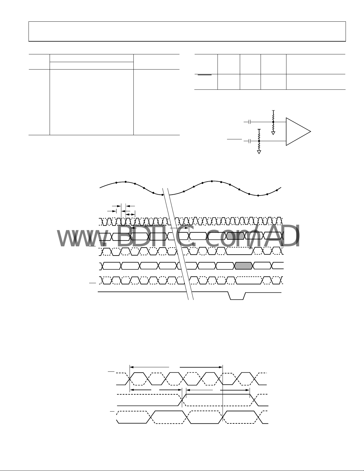
ENC
400MHZ
DATA OUT A
N– 1
t
EL
t
EH
N + 1
N + 2
N + 3
1/f
S
74 CLOCK CYCLES
N – 74
N – 73
Table 8. Option Pin List with Necessary Associated Circuitry
Logic
Pin
Name
RESET
Active
High
Lev
Typ e
el
Default
Lev
Associated Circuitry
el
Within Part
Low LVTTL High 3.74 kΩ Pull-Up
DR_EN High LVTTL High Weak Pull-Up (>16 kΩ)
3.3V
100Ω
100Ω
100Ω
100Ω
PECL
DRIVER
05649-002
ENCODE
ENCODE
3.3V
Figure 2. ENCODE Equivalent Circuit
N
N + 2
1
N + 4 N + 6 N + 8
DRA
DRA
DATA OUT B
DRB
DRB
DR_EN
NOTES
1. DATA LOST DUE TO ASSERTION OF DR_EN. LATENCY OF 74 ENCODE CLOCK CYCLES BEFORE DATA VALID.
2. IF A SINGLE-ENDED SINE WAVE IS USED FOR ENCODE, USE THE ZERO CROSSING POINT (AC-COUPLED) AS
THE 50% POINT AND APPLY THE SAME TIMING INFORMATION.
3. THE DR_EN PIN IS USED TO SYNCHRONIZE THE COLLECTION OF DATA INTO EXTERNAL BUFFER MEMORIES.
THE DR_EN PIN CAN BE APPLIED SYNCHRONOUSLY OR ASYNCHRONOUSLY TO THE AD12401. IF APPLIED
ASYNCHRONOUSLY, DR_EN MUST BE HELD LOW FOR A MINIMUM OF 5ns TO ENSURE CORRECT OPERATION.
THE FUNCTION SHUTS OFF DRA AND DRB UNTIL THE DR_EN PIN IS SET HIGH AGAIN. DRA AND DRB RESUME
ON THE NEXT VALID DRA AFTER DR_EN IS RETURNED HIGH. IF THIS FEATURE IS NOT REQUIRED, TIE THIS
PIN TO 3.3V THROUGH A 3.74kΩ RESISTOR OR LEAVE IT FLOATING.
N + 1
N + 3 N + 5 N + 7
1
Figure 3. Timing Diagram
t
EDR
ENC
ENC
DATA OUT
DR
DR
t
PD
t
VD
Figure 4. Highlighted Timing Diagram
05649-004
05649-003
Rev. A | Page 9 of 28
Page 10

AD12401
www.BDTIC.com/ADI
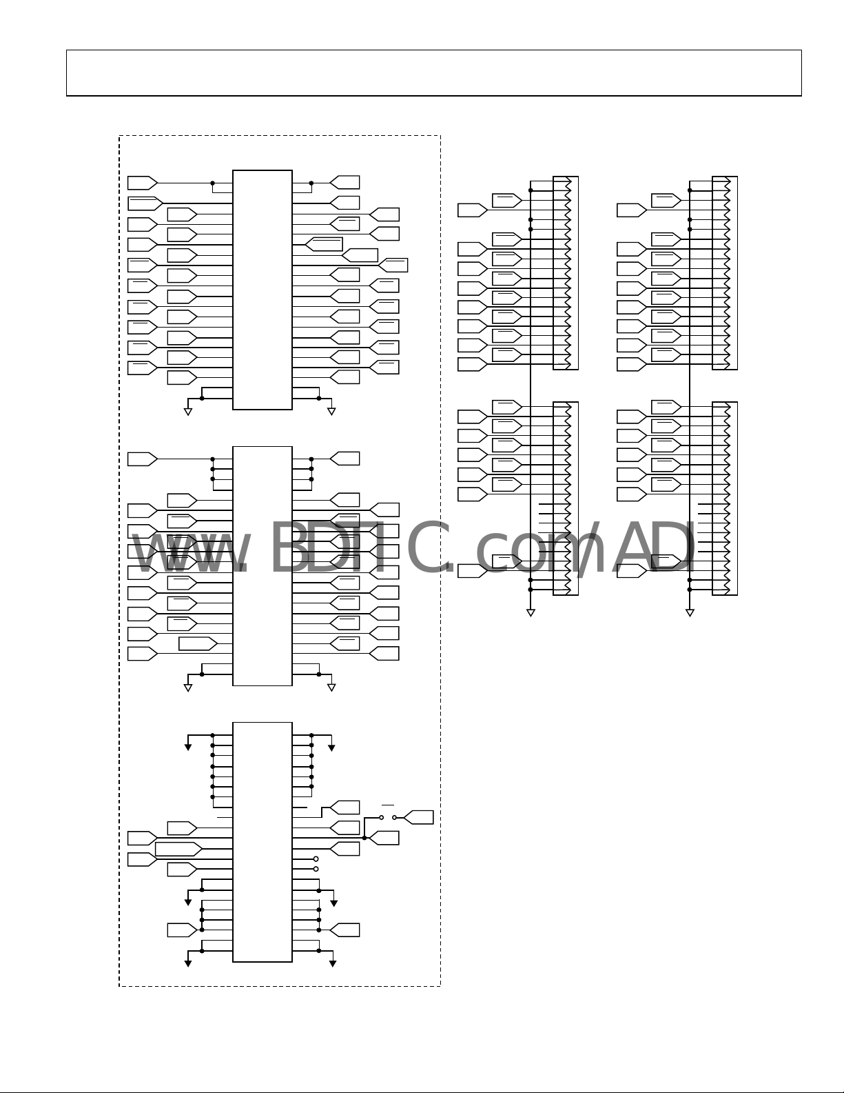
PIN CONFIGURATION AND FUNCTION DESCRIPTIONS
AIN
ENC
ENC
TOP VIEW
JOHNSON SMA-50 Ω CONNECT NO. 142-0711-821
2-56 STUDS 4⋅
END VIEW
SAMTEC CONNECT OR
QTE-060-01-L-D-A-K-TR
ENC
ENC
AIN
BOTTOM VIEW
NOTE:
1. FOR MATING CONNECT OR, USE SAMTEC, INC.
PART NO. QSE-60-01-L - D-A-K.
INTEGRAL GROUND PLANE CO NNE CTIONS.
SECTIO N A = DGND, PINS 121–12 4.
SECTIO N B = DGND, PINS 125–12 8.
SECTIO N C = AGND, PINS 129–13 2.
PIN 1
LEFT SIDE VIEW
Figure 5. Pin Configuration
BOARD
PIN 119
PIN 79
PIN 39
PIN 1
VA
VA
VA
VA
AGND
AGND
DNC
DNC
H/L_GAIN
DNC
DNC
DNC
AGND
AGND
AGND
AGND
AGND
AGND
AGND
AGND
DNC
DR_EN
DA1
DA1
DA3
DA3
DA5
DA5
DA7
DA7
DA9
DA9
DA11
DA11
DNC
DNC
VD
VD
VD
VD
DB1
DB1
DB3
DB3
DB5
DB5
DB7
DB7
DB9
DB9
DB11
DB11
DNC
DNC
DNC
DNC
DNC
RESET
VC
VC
1
VA
VA
VA
VA
AGND
AGND
DNC
DNC
DNC
DNC
DNC
DNC
DNC
AGND
AGND
AGND
AGND
AGND
AGND
AGND
1
DRA
DRA
DA0
DA0
DA2
DA2
DA4
DA4
DA6
DA6
DA8
DA8
DA10
DA10
DNC
DNC
VD
VD
VD
VD
1
DB0
DB0
DB2
DB2
DB4
DB4
DB6
DB6
DB8
DB8
DB10
DB10
OROUT
OROUT
DRB
DRB
DNC
DNC
VC
VC
PIN 120
C
PIN 80
B
PIN 40
A
PIN 2
05649-005
Rev. A | Page 10 of 28
Page 11

AD12401
www.BDTIC.com/ADI
Table 9. Pin Function Descriptions
Pin No. Mnemonic Description
1 to 4 VC Digital Supply, 3.3 V.
5
6 to 9, 11, 13 ,15,
49 to 52, 79, 96 to
102, 104 to108
10
12 DRB Channel B Data Ready. True output.
14
16 OROUT Overrange. True Output 1 = overranged, 0 = normal operation.
17
18
19 DB11 Channel B Data Bit 11. True output bit.
20 DB10 Channel B Data Bit 10. True output bit.
21
22
23 DB9 Channel B Data Bit 9. True output bit.
24 DB8 Channel B Data Bit 8. True output bit.
25
26
27 DB7 Channel B Data Bit 7. True output bit.
28 DB6 Channel B Data Bit 6. True output bit.
29
30
31 DB5 Channel B Data Bit 5. True output bit.
32 DB4 Channel B Data Bit 4. True output bit.
33
34
35 DB3 Channel B Data Bit 3. True output bit.
36 DB2 Channel B Data Bit 2. True output bit.
37
38
39 DB1 Channel B Data Bit 1. True output bit.
40 DB0 Channel B Data Bit 0. True output bit. DB0 is LSB.
41 to 48 VD Digital Supply, 1.5 V.
53
54
55 DA11 Channel A Data Bit 11. True output bit.
56 DA10 Channel A Data Bit 10. True output bit.
57
58
59 DA9 Channel A Data Bit 9. True output bit.
60 DA8 Channel A Data Bit 8. True output bit.
61
62
63 DA7 Channel A Data Bit 7. True output bit.
64 DA6 Channel A Data Bit 6. True output bit.
65
66
67 DA5 Channel A Data Bit 5. True output bit.
68 DA4 Channel A Data Bit 4. True output bit.
RESET
DNC Do Not Connect.
DRB
OROUT
DB11
DB10
DB9
DB8
DB7
DB6
DB5
DB4
DB3
DB2
DB1
DB0
DA11
DA10
DA9
DA8
DA7
DA6
DA5
DA4
LVTTL. 0 = device reset. Minimum width = 200 ns. Device resumes operation after 600 ms maximum.
Channel B Data Ready. Complement output.
Overrange. Complement output.
Channel B Data Bit 11. Complement output bit.
Channel B Data Bit 10. Complement output bit.
Channel B Data Bit 9. Complement output bit.
Channel B Data Bit 8. Complement output bit.
Channel B Data Bit 7. Complement output bit.
Channel B Data Bit 6. Complement output bit.
Channel B Data Bit 5. Complement output bit.
Channel B Data Bit 4. Complement output bit.
Channel B Data Bit 3. Complement output bit.
Channel B Data Bit 2. Complement output bit.
Channel B Data Bit 1. Complement output bit.
Channel B Data Bit 0. Complement output bit. DB0 is LSB.
Channel A Data Bit 11. Complement output bit.
Channel A Data Bit 10. Complement output bit.
Channel A Data Bit 9. Complement output bit.
Channel A Data Bit 8. Complement output bit.
Channel A Data Bit 7. Complement output bit.
Channel A Data Bit 6. Complement output bit.
Channel A Data Bit 5. Complement output bit.
Channel A Data Bit 4. Complement output bit.
Rev. A | Page 11 of 28
Page 12

AD12401
www.BDTIC.com/ADI
Pin No. Mnemonic Description
69
70
71 DA3 Channel A Data Bit 3. True output bit.
72 DA2 Channel A Data Bit 2. True output bit.
73
74
75 DA1 Channel A Data Bit 1. True output bit.
76 DA0 Channel A Data Bit 0. True output bit. DA0 is LSB.
77 DR_EN Data Ready Enable, Typically DNC. See the DR_EN section.
78
80 DRA Channel A Data Ready. True output.
103 H/L GAIN Gain Select Pin. Ground for low gain mode (KWS); pull up to 3.3 V for high gain mode (JWS).
81 to 95, 109 to 112,
129 to 132
113 to 120 VA Analog Supply, 3.7 V.
121 to 128
1
Internal ground plane connections: Section A = DGND, Pin 121 to Pin 124; Section B = DGND, Pin 125 to Pin 128; Section C = AGND, Pin 129 to Pin 132.
1
1
DA3
DA2
DA1
DA0
DRA
AGND Analog Ground.
DGND Digital Ground.
Channel A Data Bit 3. Complement output bit.
Channel A Data Bit 2. Complement output bit.
Channel A Data Bit 1. Complement output bit.
Channel A Data Bit 0. Complement output bit. DA0 is LSB.
Channel A Data Ready. Complement output.
Rev. A | Page 12 of 28
Page 13

AD12401
www.BDTIC.com/ADI
TERMINOLOGY
Analog Bandwidth
The analog input frequency at which the spectral power of the
undamental frequency (as determined by the FFT analysis) is
f
reduced by 3 dB.
Aperture Delay
The delay between the 50% point on the rising edge of the
EN
CODE command and the instant at which the analog input
is sampled.
Analog Input VSWR (50 Ω)
VSWR is a ratio of the transmitted and reflected signals. The
V
SWR can be related to input impedance.
− ZS)/(ZL + ZS)
Γ = (Z
L
where:
Z
= actual load impedance.
L
Z
= reference impedance.
S
VSWR = (1 − |Γ
Aperture Uncertainty (Jitter)
The sample-to-sample variation in aperture delay.
Differential Nonlinearity
The deviation of any code width from an ideal 1 LSB step.
Distortion, Image Spur
The ratio of the rms signal amplitude to the rms signal amplit
ude of the image spur, reported in dBFS. The image spur, a
result of gain and phase errors between two time-interleaved
conversion channels, is located at f
Distortion, Offset Spur
The ratio of the rms signal amplitude to the rms signal ampli-
de of the offset spur, reported in dBFS. The offset spur, a
tu
result of offset errors between two time-interleaved conversion
channels, is located at f
|)/(1 +|Γ|)
/2.
S
/2 − f
S
AIN
.
Full-Scale Input Power
Expressed in dBm. Computed using the equation
POWER
Full-Scale Input Voltage Range
The maximum peak-to-peak input signal magnitude that results
in a full-scale response, 0 dBFS on a single-tone input signal
case. Any magnitude increase from this value results in an
overrange condition.
Gain Error
The difference between the measured and ideal full-scale input
voltage range of the ADC.
Harmonic Distortion, Second
The ratio of the rms signal amplitude to the rms value of the
second harmonic component, reported in dBFS.
Harmonic Distortion, Third
The ratio of the rms signal amplitude to the rms value of the
third harmonic component, reported in dBFS.
Integral Nonlinearity
The deviation of the transfer function from a reference line
measured in fractions of 1 LSB using a best straight line
determined by a least square curve fit.
Maximum Conversion Rate
The maximum ENCODE rate at which the image spur calibration
degrades no more than 1 dB (when the image spur is 70 dB).
Minimum Conversion Rate
The minimum ENCODE rate at which the image spur calibration
degrades no more than 1 dB (when the image spur is 70 dB).
Offset Error
The dc offset imposed on the input signal by the ADC, reported
in LSB (codes).
= 10 log ((V2Full-Scale
Full-Scale
rms
)/(|Z
| × 0.001))
INPUT
Effective Number of Bits (ENOB)
Calculated from the measured SNR based on the equation
dB761..SNR
ENOB
ENCODE Pulse Width/Duty Cycle
Pulse width high is the minimum amount of time the ENCODE
pulse should be left in Logic 1 state to achieve rated performance; pulse width low is the minimum time the ENCODE pulse
should be left in low state.
MEASURED
=
−
026
Rev. A | Page 13 of 28
Output Propagation Delay
The delay between a differential crossing of ENCODE and
ENCODE
Pipeline Latency
The number of clock cycles the output data lags the corresponding clock cycle.
Power Supply Rejection Ratio (PSRR)
The ratio of power supply voltage change to the resulting ADC
output voltage change.
(or zero crossing of a single-ended ENCODE).
Page 14

AD12401
www.BDTIC.com/ADI
Signal-to-Noise-and-Distortion (SINAD)
The ratio of the rms signal amplitude (set 1 dB below full scale)
to the rms value of the sum of all other spectral components,
including harmonics, but excluding dc and image spur.
Signal-to-Noise Ratio (SNR)
The ratio of the rms signal amplitude (set at 1 dB below full
scale) to the rms value of the sum of all other spectral components, excluding the first five harmonics and dc.
Spurious-Free Dynamic Range (SFDR)
The ratio of the rms signal amplitude to the rms value of the
peak spurious spectral component, except the image spur. The
peak spurious component may or may not be a harmonic. It can
be reported in dBc (that is, degrades as signal level is lowered)
or dBFS (always related back to converter full-scale).
Tot a l N ois e
Calculated as
SignalSNRFS
−−
dBcdBm
dBFS
NOISE
where:
Z is the input impedance.
FS is t
he full scale of the device for the frequency in question.
SNR is t
Signal is
full scale. This value includes both thermal and quantization noise.
Two-Tone Intermodulation Distortion Rejection
The ratio of the rms value of either input tone to the rms value
of the worst third-order intermodulation product; reported in dBc.
Two -Tone SFDR
The ratio of the rms value of either input tone to the rms value
of the peak spurious component. The peak spurious component
may or may not be an IMD product. It can be reported in dBc
(that is, degrades as signal level is lowered) or in dBFS (always
related back to converter full-scale).
ZV
he value of the particular input level.
the signal level within the ADC reported in dB below
××=
10001.0
10
)(
Rev. A | Page 14 of 28
Page 15

AD12401
www.BDTIC.com/ADI
TYPICAL PERFORMANCE CHARACTERISTICS
0
1
–10
–20
–30
–40
–50
dB
–60
–70
–80
–90
–100
–110
Figure 6. FFT: f
3
5
2
0 20 40 60 80 100 120 140 160 180 200
6
4
FREQUENCY (MHz)
= 400 MSPS, AIN = 10.123 MHz @ –1.0 dBFS;
S
SNR = 63.26dB
SFDR = 76.77dBc
SINAD = 62.97dB
IMAGE SPUR = –76.69dBc
X = Image Spur, N = Interleaved Offset Spur
0
–10
–20
–30
–40
–50
dB
–60
–70
–80
–90
–100
–110
6
0 20 40 60 80 100 120 140 160 180 200
Figure 7. FFT: f
1
5
FREQUENCY (MHz)
= 400 MSPS, AIN = 70.123 MHz @ –1.0 dBFS;
S
SNR = 62.61dB
SFDR = 78.03dBc
SINAD = 62.41dB
IMAGE SPUR = –86.28dBc
2
X
4
X = Image Spur, N = Interleaved Offset Spur
0
SNR = 61.54dB
–10
SFDR = 74.03dBc
SINAD = 60.92dB
–20
IMAGE SPUR = –75.09dBc
–30
–40
–50
dB
–60
–70
3
–80
–90
–100
–110
6
0 20 40 60 80 100 120 140 160 180 200
Figure 8. FFT: f
X
FREQUENCY (MHz)
= 400 MSPS, AIN = 128.123 MHz @ –1.0 dBFS;
S
1
2
4
5
X = Image Spur, N = Interleaved Offset Spur
X
N
05649-006
N
3
05649-007
N
05649-008
0
SNR = 60.74dB
–10
SFDR = 71.57dBc
SINAD = 60.29dB
–20
IMAGE SPUR = –82.52dBc
–30
–40
–50
dB
–60
–70
–80
–90
–100
–110
0 20 40 60 80 100 120 140 160 180 200
Figure 9. FFT: f
2
X
S
5
FREQUENCY (MHz)
= 400 MSPS, AIN = 175.123 MHz @ –1.0 dBFS;
3
4
6
X = Image Spur, N = Interleaved Offset Spur
0
2
1
2F2 – F1
2F1 – F2
F2 – F1
0 20 40 60 80 100 120 140 160 180 200
2F1 + F2
F2 + F1
2F2 + F1
FREQUENCY (MHz)
dB
–100
–110
–10
–20
–30
–40
–50
–60
–70
–80
–90
Figure 10. Two-Tone Intermodulation Distortion
(25.
1 MHz and 28.1 MHz; f
= 400 MSPS);
S
X = Image Spur, N = Interleaved Offset Spur
0
–10
–20
–30
–40
–50
dB
–60
–70
–80
F2 + F1
–90
–100
–110
0 20 40 60 80 100 120 140 160 180 200
1
2
2F1 – F2
2F2 – F1
FREQUENCY (MHz)
F2 + F1
Figure 11. Two-Tone Intermodulation Distortion
(70.
1 MHz and 73.1 MHz; f
= 400 MSPS);
S
X = Image Spur, N = Interleaved Offset Spur
1
N
05649-009
05649-010
2F1 + F2
2F2 + F1
05649-011
Rev. A | Page 15 of 28
Page 16

AD12401
www.BDTIC.com/ADI
0
–10
–20
–30
–40
–50
dB
–60
–70
F2 – F1
–80
–90
–100
–110
0 20 40 60 80 100 120 140 160 180 200
F2 + F1
FREQUENCY (MHz)
2F1 + F2
2F2 + F1
Figure 12. Two-Tone Intermodulation Distortion
(17
2.1 MHz and 175.1 MHz; f
= 400 MSPS), SFDR = 70 dBc;
S
X = Image Spur, N = Interleaved Offset Spur
1
2F1 – F2
2
2F2 – F1
05649-012
95
90
85
80
75
SECOND HARMONIC
HARMONICS (dBc)
70
65
60
0 20 40 60 80 100 120 140 160 180
THIRD HARMONIC
ANALOG INPUT FREQUENCY (MHz)
IMAGE SPUR
Figure 15. Harmonics vs. Analog Input Frequency
05649-042
0.5
0.4
0.3
0.2
0.1
0
GAIN (dB)
–0.1
–0.2
–0.3
–0.4
–0.5
10.7 35.0 59.3 83.6 108 132 157 181 205 229
FREQUENCY (MHz)
05649-040
Figure 13. Interleaved Gain Flatness
100
95
90
85
80
IMAGE SPUR
75
DISTORTION (dBFS)
70
65
60
05040302010 70
ANALOG INPUT LEVEL (dB)
THIRD HARMONIC
SECOND HARMONIC
60
05649-041
Figure 14. Second/Third Harmonics and Image Spur vs. Analog Input Level;
= 400 MSPS, A
f
S
= 70 MHz
IN
64.5
64.0
63.5
63.0
62.5
62.0
SNR (dBFS)
61.5
61.0
60.5
60.0
59.5
1.0
0.9
0.8
0.7
0.6
0.5
VD SUPPLY CURRENT (A)
0.4
0.3
ANALOG INPUT FREQUENCY (MHz)
Figure 16. SNR vs. Analog Input Frequency
806040200
INPUT FREQUENCY (MHz)
Figure 17. VD Supply Current vs. A
Frequency
IN
200150100500
180160140120100 200
05649-016
05649-017
Rev. A | Page 16 of 28
Page 17

AD12401
www.BDTIC.com/ADI
–1.00
–1.42
–1.84
–2.26
–2.68
–3.10
–3.52
–3.94
ANALOG INPUT LEVEL
–4.36
–4.78
–5.20
0.100 0.530 0.960 1.390 1.820 2.250 2.680 3.110 3.540 3.970
ANALOG INPUT FREQUENCY
Figure 18. Low Frequency Gain Flatness
4.400
05649-043
Rev. A | Page 17 of 28
Page 18

AD12401
www.BDTIC.com/ADI
THEORY OF OPERATION
The AD12401 uses two high speed, 12-bit ADCs in a timeinterleaved configuration to double the sample rate, while
maintaining a high level of dynamic range performance. The
digital output of each ADC channel is calibrated using a
proprietary digital postprocessing technique, Advanced Filter
Bank (AFB). AFB is implemented using a state-of-the-art field
programmable gate array (FPGA) and provides a wide
bandwidth and wide temperature match for any gain, phase,
and clock timing errors between each ADC channel.
TIME-INTERLEAVING ADCS
When two ADCs are time-interleaved, gain and/or phase
mismatches between each channel produce an image spur at
/2 − f
f
S
mismatches can be the result of any combination of device
tolerance, temperature, and frequency deviations.
Figure 20 shows the performance of a similar converter with
on-board AFB postprocessing implemented. The –44 dBFS
image spur has been reduced to –77 dBFS and, as a result, the
dynamic range of this time-interleaved ADC is no longer
limited by the channel matching.
and an offset spur, as shown in Figure 19. These
AIN
0
–10
–20
–30
–40
–50
–60
dB
–70
–80
–90
–100
–110
–120
0 20 40 60 80 100 120 140 160 180 200
Figure 19. Image Spur due to Mismatches Between Two Interleaved ADCs
0
–10
–20
–30
–40
–50
–60
dB
–70
–80
–90
–100
–110
–120
0 20 40 60 80 100 120 140 160 180 200
Figure 20. AD12401 with AFB Digital Postprocessing
IMAGE SPUR
X
2
5
FREQUENCY (MHz)
AFB Digital Postprocessing)
(No
IMAGE SPUR
X
2
5
FREQUENCY (MHz)
OFFSET SPUR
3
4
OFFSET SPUR
3
1
N
6
05649-018
1
N
6
4
05649-019
The relationship between image spur and channel mismatches
is captured in Tab l e 10 for specific conditions.
Table 10. Image Spur vs. Channel Mismatch
Gain Error (%) Aperture Delay Error (ps) Image Spur (dBc)
1 15 –40
0.25 2.7 –54
0.2 1.1
–62
0.025 0.5 –70
For a more detailed description of time-interleaving in ADCs and a
design example using the AD12401, see Advanced Digital Post-
P
rocessing Techniques Enhance Performance in Time-Interleaved
ADC Systems, which was published in the August, 2003 edition of
e Analog Dialogue (www.analog.com/analogDialogue).
th
ANALOG INPUT
The AD12401 analog input is ac-coupled using a proprietary
transformer front-end circuit that provides 1 dB of gain flatness
over the first Nyquist zone and a −3 dB bandwidth of 480 MHz.
This front-end circuit provides a VSWR of 1.5 (50 Ω) over the
first Nyquist zone, and the typical full-scale input is 3.2 V p-p.
The Mini-Circuits® HELA-10 amplifier module can be used to
drive the input at these power levels.
CLOCK INPUT
The AD12401 requires a 400 MSPS ENCODE that is divided by 2
and distributed to each ADC channel, 180° out of phase from
each other. Internal ac-coupling and bias networks provide the
framework for flexible clock input requirements that include
single-ended sine wave, single-ended PECL, and differential
PECL. While the AD12401 is tested and calibrated using a
single-ended sine wave, properly designed PECL circuits that
provide fast slew rates (>1 V/ns) and minimize ringing result in
comparable dynamic range performance.
Aperture jitter and harmonic content are two major factors to
c
onsider when designing the input clock circuit for the AD12401.
The relationship between aperture jitter and SNR can be
characterized using the following equation. The equation
assumes a full-scale, single-tone input signal.
SNR =
2
⎡
⎢
()
⎢
⎢
⎣
where:
f
= input frequency.
A
t
= aperture jitter.
JRMS
ADC resolution (bits).
N =
ε = ADCDNL (LSB).
V
= ADC input noise (LSB rms).
NOISErms
2
⎛
×
V
ε+
1
1
⎛
2
tf
020log20
JRMSA
×+××π−
⎜
N
2
5.1
⎝
22
⎞
⎜
+
⎟
⎜
⎠
⎝
NOISErms
N
2
⎤
⎞
⎥
⎟
⎟
⎥
⎠
⎥
⎦
Rev. A | Page 18 of 28
Page 19

AD12401
www.BDTIC.com/ADI
Figure 21 displays the application of this relationship to a fullscale, single-tone input signal on the AD12401, where the DNL
was assumed to be 0.4 LSB, and the input noise was assumed to
be 0.8 LSB rms. The vertical marker at 0.4 ps displays the SNR
at the jitter level present in the AD12401 evaluation system,
including the jitter associated with the AD12401 itself.
65
64
63
62
61
SNR (dB)
60
59
58
57
0 0.1 0.2 0.3 0.4 0.5 0.6 0.7 0.8 0.9 1.0
APERTURE JITTER (ps rms)
Figure 21. SNR vs. Aperture Jitter
= 180MHz
A
IN
AIN = 10MHz
A
= 65MHz
IN
A
= 128MHz
IN
05649-020
In addition to jitter, the harmonic content of the single-ended
sine wave clock sources must be controlled. The clock source
used in the test and calibration process has a harmonic performance that is better than 60 dBc. Additionally, when using
PECL or other square-wave clock sources, unstable behavior,
such as overshoot and ringing, can affect phase matching and
degrade the image spur performance.
DIGITAL OUTPUTS
The AD12401’s digital postprocessing circuit provides two
parallel, 12-bit, 200 MSPS data output buses. By providing two
output busses that operate at one half the conversion rate, the
AD12401 eliminates the need for large, expensive, high power
demultiplexing circuits. The output data format is twos complement, maintaining the standard set by other high speed
ADCs, such as the
pr
ovided for facilitating proper timing in the data capture circuit.
AD9430 and AD6645. Data-ready signals are
POWER SUPPLIES
The AD12401 requires three different supply voltages: a 1.5 V
supply for the digital postprocessing circuit, a 3.3 V supply to
facilitate digital I/O through the system, and a 3.8 V supply for
the analog conversion and clock distribution circuits. The
AD12401 incorporates two key features that result in solid
PSRR performance. First, on-board linear regulators are used to
provide an extra level of power supply rejection for the analog
circuits. The linear regulator used to supply the ADCs provides
an additional 60 dB of rejection at 100 kHz. Second, to address
higher frequency noise (where the linear regulators’ rejection
degrades), the AD12401 incorporates high quality ceramic
decoupling capacitors.
While this product was designed to provide good PSRR
p
erformance, system designers need to be aware of the risks
associated with switching power supplies and consider using
linear regulators in their high speed ADC systems. Switching
power supplies typically produces both conducted and radiated
energy that result in common-/differential-mode EMI currents.
Any system that requires 12-bit performance has very little
room for errors associated with power supply EMI. For example, a system goal of 74 dB dynamic range performance on the
AD12401 requires noise currents that are less than 4.5 μA and
noise voltages of less than 225 μV in the analog input path.
STARTUP AND RESET
The AD12401’s FPGA configuration is stored in the on-board
EPROM and loaded into the FPGA when power is applied to
the device. The
pin (active low) allows the user to reload
RESET
the FPGA in case of a low digital supply voltage condition or a
power supply glitch. Pulling the
pin low pulls the data-
RESET
ready and output bits high until the FPGA is reloaded. The
pin should remain low for a minimum of 200 ns. On the
RESET
rising edge of the reset pulse, the AD12401 starts loading the
configuration into the FPGA. The reload process requires a
maximum of 87 ms to complete. Valid signals on the data-ready
pins indicate the reset process is complete. In addition, system
designers must be aware of the thermal conditions of the
AD12401 at startup. If large thermal imbalances are present, the
AD12401 can require additional time to stabilize before providing
specified image spur performance.
DR_EN
The DR_EN pin is used to synchronize the collection of data
into external buffer memories. DR_EN must be held low for a
minimum amount of time (see Tabl e 2 through Ta b le 4 for each
CODE rate) to ensure correct operation. The function shuts
EN
off DRA and DRB until the DR_EN pin is set high again. DRA
and DRB resume on the next valid DRA after DR_EN is
released. If this feature is not required, tie this pin to 3.3 V
through a 3.74 kΩ.
OVERRANGE
The differential OROUT pins are used to determine if the
AD12401 input is overranged. OROUT timing is identical to the
Channel B data. If the OROUT pin is high, then the Channel B
data coincident with the overrange indication or the Channel A
data immediately preceding it resulted from an overrange input.
If the OROUT pin is low, the operation is normal.
Rev. A | Page 19 of 28
Page 20

AD12401
R
A
www.BDTIC.com/ADI
GAIN SELECT
The AD12401 is graded out for the gain mode and should be
ordered accordingly: the AD12401-xxxKWS is calibrated in the
low gain mode, and the AD12401-xxxJWS is calibrated in the
high gain mode. Performance is not guaranteed if either grade
is used in the wrong gain mode.
The high gain mode sets the analog input voltage to
pproximately 1.6 V p-p. The low gain mode sets the analog
a
input voltage to approximately 3.2 V p-p. For high gain mode,
the user should pull Pin 103 (H/L_GAIN) up to 3.3 V using
a 4.02 kΩ resistor. For low gain mode, the user should ground
Pin 103.
THERMAL CONSIDERATIONS
The module is rated to operate over a case temperature of 0°C
to 60°C. To maintain the tight channel matching and reliability
of the AD12401, care must be taken to ensure that proper
thermal and mechanical considerations have been made and
addressed to ensure case temperature is kept within this range.
Each application requires evaluation of the thermal management as applicable to the system design. This section provides
information that should be used in the evaluation of the
AD12401’s thermal management for each specific use.
In addition to the radiation of heat into its environment, the
AD12401
mounting studs and standoffs as they contact the motherboard.
As described in the
s
ection, the module should be secured to the motherboard
using 2-56 nuts (washer use is optional). The torque on the nuts
should not exceed 32-inch ounces. Using a thermal grease at the
standoffs results in better thermal coupling between the board
and module. Depending on the ambient conditions, airflow can
be necessary to ensure the components in the module do not
exceed their maximum operating temperature. For reliability,
the most sensitive component has a maximum junction
temperature rating of 125°C.
Figure 22 and Figure 23 provide a basic guideline for two key
hermal management decisions: the use of thermal interface
t
material between the module bottom cover/mother board and
airflow. Figure 21 characterizes the typical thermal profile of an
AD12401 tha
rovides the same information for a configuration that uses
p
gap-filling thermal interface material. In this case, Thermagon
T-flex 600 Series™, 0.040” thickness, was used. These profiles
show that the maximum die temperature is reduced by
approximately 2°C when thermal interface material is used.
Figure 22 and Figure 23 also provide a guideline for determining
he airflow requirements for given ambient conditions. For
t
example, a goal of 120°C die temperature in a 40°C ambient
environment without the use of thermal interface material
requires an airflow of 100 LFM.
module enables the flow of heat through the
Package Integrity/Mounting Guidelines
t is not using thermal interface material. Figure 22
From a channel-matching perspective, the most important
nsideration is external thermal influences. It is possible for
co
thermal imbalances in the end application to adversely affect
the dynamic performance. Due to the temperature dependence
of the image spur, substantial deviation from the factory calibration conditions can have a detrimental effect. Unbalanced
thermal influences can cause gradients across the module, and
performance degradation can result. Examples of unbalanced
thermal influences can include large heat dissipating elements
near one side of the AD12401, or obstructed airflow that does
not flow uniformly across the module. The thermal sensitivity
of the module can be affected by a change in thermal gradient
across the module of 2°C.
110
100
90
80
70
TURE (°C)
60
50
TEMPE
40
30
20
NO AIRFL OW 100 LFM 300 LFM
Figure 22. Typical Temperature vs. Airflow with No Module/Board
Interfa
ce Material (Normalized to 60°C Module Case Temperature)
110
100
90
80
70
60
50
TEMPERATURE (°C)
40
30
20
NO AIRFLOW 100 LFM 300 LFM
Figure 23. Typical Temperature vs. Airflow with T-flex Module/Board
Interfa
ce Material (Normalized to 60°C Module Case Temperature Ambient)
TYPICAL JUNCTION
CASE
AMBIENT
AIRFLOW CO NDITION
TYPICAL JUNCTION
CASE
AMBIENT
AIRFLOW CONDITION
05649-021
05649-022
PACKAGE INTEGRITY/MOUNTING GUIDELINES
The AD12401 is a printed circuit board (PCB)-based module
designed to provide mechanical stability and to support the
intricate channel-to-channel matching necessary to achieve high
dynamic range performance. The module should be secured to
the motherboard using 2-56 nuts (washer use is optional). The
torque on the nuts should not exceed 32-inch ounces.
Rev. A | Page 20 of 28
Page 21

AD12401
www.BDTIC.com/ADI
The SMA edge connectors (AIN and ENC/
mounted to the board to achieve minimum height of the
module. When attaching and routing the cables, one must
ensure they are stress-relieved and do not apply stress to the
SMA connector/board. The presence of stress on the cables can
degrade electrical performance and mechanical integrity of the
module. In addition to the routing precautions, the smallest
torque necessary to achieve consistent performance should be
used to secure the system cable to the AD12401’s SMA
connectors. The torque should never exceed 5-inch pounds.
Any disturbances to the AD12401 structure, including
moving the covers or mounting screws, invalidates the
re
calibration and results in degraded performance. See the
Outline Dimensions section for mounting stud dimensions, see
Figure 38 for PCB interface locations. Mounting stud length
typ
ically accommodates a PCB thickness of 0.093". Consult
sales if board thickness requirements exceed this dimension.
AD12401 EVALUATION KIT
The AD12401/KIT offers an easy way to evaluate the AD12401.
The AD12401/KIT includes the AD12401 mounted on an
adapter card, the AD12401 evaluation board, the power supply
cables, a 225 MHz buffer memory FIFO board, and the Dual
Analyzer software. The user must supply a clock source, an
analog input source, a 1.5 V power supply, a 3.3 V power supply,
a 5 V power supply, and a 3.8 V power supply. The clock source
and analog input source connect directly to the AD12401. The
power supply cables (included) and a parallel port cable (not
included) connect to the evaluation board. The AD12401
works on the same evaluation board as the AD12400 and the
AD12500: GS08054.
Power Connector
Power is supplied to the board via a detachable 12-lead power
strip (three 4-pin blocks).
Table 11. Power Connector
Supply Description
VA 3.7 V Analog supply for the ADC (950 mA typ)
VC 3.3 V Digital supply for the ADC outputs (400 mA typ)
VD 1.5 V1Digital supply for the FPGA (1.25 A max, 0.7 A typ)
VB 5.0 V Digital supply for the buffer memory board (400 mA typ)
1
The power supply cable has an approximately 100 mV drop. The VD supply
current is dependent on the analog input frequency (see Figure 17).
Analog Input
The analog input source connects directly to an SMA on the
AD12401.
) are surface
ENC
ENCODE
The single-ended or differential ENCODE signal connects directly
to SMA connector(s) on the AD12401. A single-ended sine wave
at 10 dBm connected to the ENCODE SMA is recommended.
A low jitter clock source (<0.5 ps) is recommended to properly
eval
uate the AD12401.
DATA OUTPUTS
The AD12401xxxKWS digital outputs are available at the 80-pin
connector, P2, on the evaluation board. The AD12401/KIT
comes with a buffer memory FIFO board connected to P2,
which provides the interface to the parallel port of a PC. The
Dual Analyzer software is compatible with Windows® 95,
Windows 98, Windows 2000, and Windows NT®.
The buffer memory FIFO board can be removed, and an external
ic analyzer or other data acquisition module can be connected
log
to this connector, if required.
Adapter Card
The AD12401 is attached to an adapter card that interfaces to
the evaluation board through a 120-pin connector, P1, which is
on the top side of the evaluation board.
Digital Postprocessing Control
The evaluation board has a 2-pin jumper, labeled AFB, that
allows the user to enable/disable the digital postprocessing. The
digital postprocessing is active when the AFB jumper is applied.
When the jumper is removed, the FPGA is set to a passthrough
mode, which demonstrates to the user the performance of the
AD12401 without the digital postprocessing.
RESET
The AD12401’s FPGA configuration is stored in an EEPROM
and loaded into the FPGA when power is applied to the AD12401.
The
the FPGA in case of a low voltage condition or a power supply
glitch. Depressing the
output bits high. The
minimum of 200 ns. On the rising edge of the
AD12401 starts loading the configuration into the on-module
FPGA. The reload process requires a maximum of 600 ms to
complete. Valid signals on the data-ready pins indicate the reset
process is complete.
The AD12401 is not compatible with the HSC-ADC-EVAL-
DC
/SC hardware or software.
switch, SW1 (active low), allows the user to reload
RESET
switch pulls the data-ready and
RESET
switch should remain low for a
RESET
RESET
pulse, the
H/L_GAIN
The H/L_GAIN select jumper, Pin 103, should be on for low
gain mode (AD12401-xxxKWS). The H/L_GAIN select jumper
should be removed for high gain mode, AD12401-xxxJWS.
Rev. A | Page 21 of 28
Page 22

AD12401
www.BDTIC.com/ADI
Table 12. Evaluation Board Bill of Materials (BOM)
Item No. Qty. Ref-Des Device Package Value, Mfg
1 2 C3, C5 Capacitors 603 0.1 μF, 25 V
2 2 C4, C6 Capacitors 805 10 μF, 6.3 V
3 1 R9 Resistor 603
4 1 AFB 2-Pin Header/Jumper Pin Strip
5 1 P2 80-Pin Dual Connector Assembly Surface-Mount
6 1 SW1 Switch Push Button SPST 6 MM
7 3 J2, J3, J4 4-Pin Header Power Connecters Pin Strip
8 1 P1 60-Pin Dual-Socket Assembly Surface-Mount
9 1 PCB AD12401 Interface Board GS08054 PCB
R8
4.02kΩ
3.3VC
PASS
3.3VC
H/L_GAIN
3.3VC
NYQ
3.3VC
OTHER
R9
4.02kΩ
R10
4.02kΩ
R11
4.02kΩ
E12
E13
AFB
H/L_GAIN
NYQ
DITHER
JP2
JP3
SPARE1
SPARE2
SPARE1
SPARE2
E14
E18
4.02 kΩ, 1%
Molex/GC/Weldon
Post Header AMP
Panasonic
Wieland
Samtec
DGND
E17
SELECT D
E1
1
2
E22
JP4
EVQ-PAC85R
1.5V SENSE
3.3VD
4
3
DGND
05649-023
DGND
1.5VD
DGND
3.3VC
5V
DIGITAL
J4
1
2
3
4
DIGITAL
J3
1
2
3
4
3.8V
AGND
+VA
ANALOG
J2
1
2
3
4
5V 5V
C4
10μFC30.1μF
DGND DGND
3.3VC
C6
10μFC50.1μF
DGND DGND
Figure 24. Evaluation Board
SELECT D
RESET
3.3VD
Rev. A | Page 22 of 28
Page 23
AD12401
A
www.BDTIC.com/ADI
AD1240X
P1:A
21
3.3VC
RESET
DNC
DNC
DB11
DB9
DB7
DB5
DB3
DB1
1.5VD
DNC
DA11
DA9
DA7
DA5
DA3
DA1
DNC
DNC
DNC
3
5
DNC
DNC
DNC
DB11
DB11
DB9
DB7
DB5
DB3
DB1
DGND
DNC
DA11
DA9
DA7
DA5
DA3
DA1
DR_EN
DGND
AGND
DNC
H/L_GAIN
DNC
AGND AGND
+VA
7
9
11
13
15
17
19
21
23
25
27
29
31
33
35
37
39
121
123
QSE–60–01–L–D–A–K
43
45
47
49
51
53
55
57
59
61
63
65
67
69
71
73
75
77
79
125
127
QSE–60–01–L–D–A–K
83
85
87
89
91
93
95
97
99
101
103
105
107
109
111
113
115
117
119
129
131
QSE–60–01–L–D–A–K
GND
GND
GND
GND
GND
P1:B
P1:C
GND
GND
GND
GND
GND
GND
4
6
8
10
12
14
16
18
20
22
24
26
28
30
32
34
36
38
40
122
124
4241
44
46
48
50
52
54
56
58
60
62
64
66
68
70
72
74
76
78
80
126
128
8281
84
86
88
90
92
94
96
98
100
102
104
106
108
110
112
114
116
118
120
130
132
OROUT
DGND
DGND
AGND
E2
E19
AGNDAGND
3.3VC
DNC
DRB
DB10
DB8
DB6
DB4
DB2
DB0
1.5VD
PASS
DA10
DA8
DA6
DA4
DA2
DA0
DRA
DNC
DNC
DNC
+VA
OROUT
DNC
DRB
DB8
DB6
DB4
DB2
DB0
DNC
DA10
DA8
DA6
DA4
DA2
DA0
DRA
WP
DNC
DB10
3.3VC
DRA
DA11
DA10
DA9
DA8
DA7
DA6
DA5
DA4
DA3
DA2
DA1
DA0
OR
DRA
DA11
DA10
DA9
DA8
DA7
DA6
DA5
DA4
DA3
DA2
DA1
DA0
OR
Figure 25. Evaluation Board
AMP104655-9
DGND
P2:C
41
42
43
44
45
46
47
48
49
50
51
52
53
54
55
56
57
58
59
60
P2:D
61
62
63
64
65
66
67
68
69
70
71
72
73
74
75
76
77
78
79
80
AMP104655-9
DRB
DB11
DB10
DB9
DB8
DB7
DB6
DB5
DB4
DB3
DB2
DB1
DB0
OR
DRB
DB11
DB10
DB9
DB8
DB7
DB6
DB5
DB4
DB3
DB2
DB1
DB0
OR
DGND
P2:A
1
2
3
4
5
6
7
8
9
10
11
12
13
14
15
16
17
18
19
20
AMP104655-9
P2:B
21
22
23
24
25
26
27
28
29
30
31
32
33
34
35
36
37
38
39
40
MP104655-9
05649-024
Rev. A | Page 23 of 28
Page 24

AD12401
www.BDTIC.com/ADI
Figure 26. Power Plane 1
Figure 27. Power Plane 2
05649-025
05649-026
Figure 29. Second Ground Plane
Figure 30. Top Side Copper
05649-028
05649-029
05649-027
Figure 28. First Ground Plane
Rev. A | Page 24 of 28
Figure 31. Bottom Side Copper
05649-030
Page 25

AD12401
www.BDTIC.com/ADI
05649-031
Figure 32. Top Mask
Figure 35. Evaluation Adapter Board, Top Silkscreen
05649-034
Figure 33. Top Silkscreen
Figure 34. Bottom Silkscreen
05649-032
05649-033
Figure 36. Evaluation Adapter Board, Analog and Digital Layers
Figure 37. Evaluation Adapter Board, Bottom Silkscreen
05649-035
05649-037
Rev. A | Page 25 of 28
Page 26

AD12401
www.BDTIC.com/ADI
LAYOUT GUIDELINES
The AD12401 requires a different approach from traditional
high speed ADC system layouts. While the AD12401’s internal
PCB isolates digital and analog grounds, these planes are tied
together through the product’s aluminum case structure.
Therefore, the decision to isolate the analog and digital grounds
on the system PCB has additional factors to consider.
For example, if the AD12401 is attached with conductive
hermal interface material to the system PCB, there is
t
essentially no benefit to keeping the analog and digital ground
planes separate. If neither thermal interface material nor
nonconductive interface material is used, system architects
must consider the ground loop that is created if analog and
digital planes are tied together directly under the AD12401.
This EMI-based decision must be considered on a case-by-case
basis and is largely dependent on the other sources of EMI in
the system. One critical consideration is that a 12-bit performance requirement (–74 dBc) requires keeping conducted EMI
currents (referenced to the input of the AD12401) below 4.5 μA.
All the characterization and testing of the AD12401 is performed
using a system that isolated these ground planes.
PCB INTERFACE
Figure 38 provides the mounting hole footprint for assembling
the AD12401 to the second-level assembly. The diagram is
referenced to the center of the mating QTE connector. Refer to
the QTE/QSE series connector documentation at www.samtec.com
for the SMT footprint of the mating connector.
The top view of the second-level assembly footprint provides a
gram of the second-level assembly locating tab locations for
dia
mating the Samtec QTE-060-01-L-A-K-TR terminal strip on
the AD12401 to a QSE-060-01-L-A-K-TR socket on the secondlevel assembly. The diagram is referenced to the center of the
QTE terminal strip on the AD12401 and the mounting holds
for the screws, which holds the AD12401 to the second-level
assembly board. The relationship of these locating tabs is based
on information provided by Samtec (connector supplier) and
should be verified with Samtec by the customer.
Mating and unmating forces—the knifing or peeling action of
a
pplying force to one end or one side—must be avoided to
prevent damage to the connector and guidepost.
If thermal interface material is used in the final system design,
e following layout factors need to be considered: open solder
th
mask on the area that contacts the interface material and the
thickness of the ground plane. While this should be analyzed in
each specific system design, the use of solder mask can negate
any advantage achieved by using the thermal interface material,
and its use should be carefully considered. The ground plane
thickness does not have a major impact on the thermal performance, but if design margin is slight, additional thickness
can yield incremental improvements.
Rev. A | Page 26 of 28
Page 27

AD12401
www.BDTIC.com/ADI
1.184 [30.0673]
1.025 [26.0164] 2×
0, 0 DATUM = CENTER OF CONNECTOR
R.0470[R1.19] 6×
0.000 [.0000]
2.159 [54.8258] 2×
Figure 38. Top View of Interface PCB Assembly
0.396 [10.0456] 2×
0.105 [2.6670] 2×
.000 [.0000]
1.025 [26.0164] 2×
1.184 [30.0673]
05649-038
Rev. A | Page 27 of 28
Page 28

AD12401
0
www.BDTIC.com/ADI
OUTLINE DIMENSIONS
3.190 TYP
2.890 MAX
PIN 1
AIN
BOARD
.700 MAX
0.175 TYP
2.060
2.040
TOP VIEW
ENC
ENC
JOHNSON SMA-50 O HM CONNECT NO. 142-07 11-821
SIDE VIEW
2-56 STUDS 4⋅
BOTTOM VIEW
0.270 2⋅
2.590 MAX
0.200 TYP
2.060
2.040
0.267 TYP
0.600 MAX
SAMTEC CONNECTOR
QTE-060-01-L-D-A-K-TR
2.328 TYP
0.856 TYP
0.256 TYP
0.505 TYP 2⋅
1.773
1.753
Figure 39. Non-Hermetic Hybrid—Surface-Mounted Parts
(WS-Suffix)
Dimensions sh
own in inches
Tolerances: 0.xxx = ±5 mils
ORDERING GUIDE
Model Temperature Range Package Description
AD12401-326KWS 0°C to 60°C (Case) 2.9" × 2.6" × 0.6" Module
AD12401-326JWS 0°C to 60°C (Case) 2.9" × 2.6" × 0.6" Module
AD12401-360KWS 0°C to 60°C (Case)
AD12401-400KWS 0°C to 60°C (Case)
AD12401-400JWS 0°C to 60°C (Case)
AD12401/KIT
1
The encode rate and gain mode must be selected when ordering the AD12401/KIT. The standard AD12401/KIT is configured for low gain mode at 400 MSPS.
©2006 Analog Devices, Inc. All rights reserved. Trademarks and
registered trademarks are the property of their respective owners.
D05649-0-4/06(A)
1
Evaluation Kit
Rev. A | Page 28 of 28
2.9" × 2.6" × 0.6" Module
2.9" × 2.6" × 0.6" Module
2.9" × 2.6" × 0.6" Module
040606-A
 Loading...