

A
G
16-Bit, 80 MSPS A/D Converter
FEATURES
80 MSPS sample rate
80 dBFS signal-to-noise ratio
Transformer-coupled analog input
Single PECL clock source
Digital outputs
True binary format
3.3 V and 5 V CMOS-compatible
APPLICATIONS
Low signature radar
Medical imaging
Communications instrumentation
Instrumentation
Antenna array processing
GENERAL DESCRIPTION
The AD10678 is a 16-bit, high performance, analog-to-digital
converter (ADC) for applications that demand increased SNR
levels. Exceptional noise performance and a typical signal-tonoise ratio of 80 dBFS are obtained by digitally postprocessing
the outputs of four ADCs. A single analog input and PECL
sampling clock and 3.3 V and 5 V power supplies are required.
The AD10678 is assembled using a 0.062" thick laminate board
with three sets of connector interface pads to accommodate
analog and digital isolation. Analog Devices recommends using
the FSI-110-03-G-D-AD-K-TR connector from Samtec. The
overall board fits a 2.2" × 2.8" PCB specified from 0°C to 70°C.
AD10678
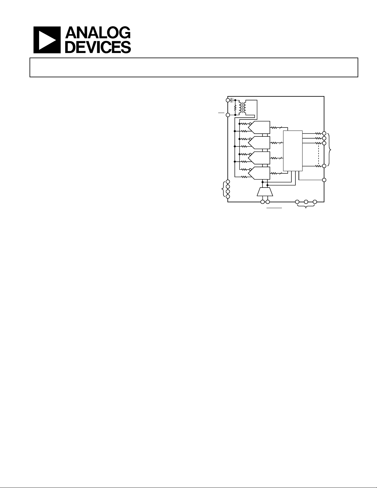
FUNCTIONAL BLOCK DIAGRAM
AIN
AIN
ADC
ADC
ADC
ADC
AGND
NALO
POWER
5VA
3.3VE
AGND
CLOCK DISTRIBUTION
CIRCUIT
Figure 1.
PRODUCT HIGHLIGHTS
1. Guaranteed sample rate of 80 MSPS.
2. Input signal conditioning with optimized noise
performance.
3. Fully tested and guaranteed performance.
AD10678
14
14
DIGITAL
POST-
PROCES-
14
SING
14
DGND DGND
DIGITAL POWERENCODE ENCODE
D
D
3.3V
OUT
OUT
0
15
OUTPUT
DATA
BITS
DRY
03376-A-001
Rev. B
Information furnished by Analog Devices is believed to be accurate and reliable.
However, no responsibility is assumed by Analog Devices for its use, nor for any
infringements of patents or other rights of third parties that may result from its use.
Specifications subject to change without notice. No license is granted by implication
or otherwise under any patent or patent rights of Analog Devices. Trademarks and
registered trademarks are the property of their respective owners.
One Technology Way, P.O. Box 9106, Norwood, MA 02062-9106, U.S.A.
Tel: 781.329.4700
Fax: 781.461.3113 © 2005 Analog Devices, Inc. All rights reserved.
www.analog.com

AD10678
TABLE OF CONTENTS
Specifications..................................................................................... 3
DC Specifications ......................................................................... 3
Digital Specifications ................................................................... 3
AC Specifications.......................................................................... 4
Switching Specifications.............................................................. 5
Absolute Maximum Ratings............................................................ 6
Explanation of Test Levels........................................................... 6
Operating Range........................................................................... 6
ESD Caution.................................................................................. 6
Test Circuits....................................................................................... 7
Pin Configurations and Function Descriptions ........................... 8
Typical Performance Characteristics ...........................................10
REVISION HISTORY
3/05—Rev. A to Rev. B
Changes to Figure 1.......................................................................... 1
Changes to Figure 2 and Figure 3................................................... 7
Added Figure 7 to Figure 9.............................................................. 8
Reformatted Table 7 ......................................................................... 8
Changes to Figure 10........................................................................ 9
Reformatted Theory of Operation Section ................................. 13
Changes to Figure 22...................................................................... 15
Terminology .................................................................................... 12
Theory of Operation ...................................................................... 13
Thermal Considerations............................................................ 13
Input Stage................................................................................... 13
Encoding the AD10678 ............................................................. 13
Output Loading .......................................................................... 13
Analog and Digital Power Supplies.......................................... 13
Analog and Digital Grounding................................................. 14
Other Notes................................................................................. 14
Evaluation Board........................................................................ 14
Outline Dimensions....................................................................... 19
Ordering Guide .......................................................................... 19
12/03—Rev. 0 to Rev. A
Updated format...................................................................Universal
Changes to AC Specifications table footnotes .............................. 4
Changes to Table 1............................................................................ 3
Changes to Table 3............................................................................ 6
Changes to Figure 11...................................................................... 10
Changes to Theory of Operation.................................................. 13
Changes to Ordering Guide.......................................................... 20
2/03—Revision 0: Initial Version
Rev. B | Page 2 of 20

AD10678
SPECIFICATIONS
DC SPECIFICATIONS
AVCC = 5 V, EVCC = 3.3 V, VDD = 3.3 V, TA = 25°C, differential encode = 80 MSPS, C
Table 1.
Parameter Test Level Min Typ Max Unit
RESOLUTION 16 Bits
Offset Error I –0.30 +0.12 +0.30 %FS
Gain Error I –7 +7 %FS
Differential Nonlinearity (DNL) V ±0.7 LSB
Integral Nonlinearity (INL) V ±4 LSB
TEMPERATURE DRIFT
Offset Error V 13 ppm/°C
Gain Error V 200 ppm/°C
POWER SUPPLY REJECTION RATIO (PSRR) V 60 dB
ANALOG INPUTS (AIN, AIN)1
Differential Input Voltage Range V 2.15 V p-p
Differential Input Resistance V 50 Ω
Differential Input Capacitance V 2.5 nF
Input Bandwidth IV 0.40 220 MHz
VSWR2 V 1.04:1 Ratio
POWER SUPPLY3
Supply Current
IAVCC (AVCC = 5.0 V) I 0.95 1.1 A
IEVCC (EVCC = 3.3 V) I 0.15 0.2 A
IVDD (VDD = 3.3 V) I 0.49 0.625 A
Total Power Dissipation4 I 6.86 8.0 W
1
Measurement includes the recommended interface connector.
2
Input VSWR, see . Figure 18
3
Supply voltages should remain stable within ±5% for normal operation.
4
Power dissipation measured with encode at rated speed and –6 dBFS analog input at 10 MHz.
≤ 10 pF, unless otherwise noted.
LOAD
DIGITAL SPECIFICATIONS
AVCC = 5 V, EVCC = 3.3 V, VDD = 3.3 V, TA = 25°C, differential encode = 80 MSPS, C
Table 2.
Parameter Test Level Min Typ Max Unit
ENCODE INPUTS (ENCODE, ENCODE)
Differential Input Voltage Range IV 0.4 V p-p
Differential Input Resistance V 100 Ω
Differential Input Capacitance V 160 pF
LOGIC OUTPUTS (D15 to D0)
Logic Compatibility CMOS
Logic 1 Voltage I
Logic 0 Voltage I
≤100 mA IV 0.9 × VDD V
LOAD
≤100 mA IV 0.4 V
LOAD
Output Coding True binary
Series Output Resistance per Bit 120 Ω
Rev. B | Page 3 of 20
≤ 10 pF, unless otherwise noted.
LOAD

AD10678
AC SPECIFICATIONS
AVCC = 5 V, EVCC = 3.3 V, VDD = 3.3 V, TA = 25°C, differential encode = 80 MSPS, C
Table 3.
Parameter Test Level Min Typ Max Unit
SNR1
Analog Input 2.5 MHz I 77.5 80.5 dBFS
@ −6 dBFS 10 MHz I 77.5 80.5 dBFS
30 MHz I 77 80.2 dBFS
70 MHz I 76 78 dBFS
SINAD2
Analog Input 2.5 MHz I 77.2 80.3 dBFS
@ −6 dBFS 10 MHz I 77.2 80.3 dBFS
30 MHz I 76.6 79.7 dBFS
70 MHz I 74.7 77.4 dBFS
SFDR3
Analog Input 2.5 MHz I 88 97.2 dBFS
@ −6 dBFS 10 MHz I 88 97.2 dBFS
30 MHz I 84 94.2 dBFS
70 MHz I 81 91.7 dBFS
TWO-TONE4
Analog Input
@ −7 dBFS IMD
f1 = 10 MHz, f2 = 12 MHz V 96 dBFS
f1 = 70 MHz, f2 = 72 MHz V 84 dBFS
1
Analog input signal power at −6 dBFS; signal-to-noise (SNR) is the ratio of signal level to total noise (first five harmonics removed). Encode = 80 MSPS. SNR is reported
in dBFS, related back to converter full scale.
2
Analog input signal power at −6 dBFS; signal-to-noise and distortion (SINAD) is the ratio of signal level to total noise + harmonics. Encode = 80 MSPS. SINAD is
reported in dBFS, related back to converter full scale.
3
Analog input signal equals −6 dBFS; SFDR is the ratio of converter full scale to worst spur.
4
Both input tones at −7 dBFS; two-tone intermodulation distortion (IMD) rejection is the ratio of either tone to the worst third-order intermodulation product.
≤ 10 pF, unless otherwise noted.
LOAD
Rev. B | Page 4 of 20
AD10678
SWITCHING SPECIFICATIONS
AVCC = 5 V, EVCC = 3.3 V, VDD = 3.3 V, TA = 25°C, differential encode = 80 MSPS, C
Table 4.
Parameter Test Level Min Typ Max Unit
MAXIMUM CONVERSION RATE I 80 MSPS
MINIMUM CONVERSION RATE IV 30 MSPS
DUTY CYCLE IV 40 60 %
ENCODE INPUTS PARAMETERS
Encode Period @ 80 MSPS, t
Encode Pulse Width High @ 80 MSPS, t
Encode Pulse Width Low @ 80 MSPS, t
V 12.5 ns
ENC
V 6.25 ns
ENCH
V 6.25 ns
ENCL
ENCODE/DATA (D15:D0)
Propagation Delay, t
Valid Time, t
7.3 ns
PDL
6.7 ns
PDH
ENCODE/DATA READY1
Encode Rising to Data Ready Falling, t
Encode Rising to Data Ready Rising, t
12.6 ns
DR_F
6.4 ns
DR_R
DATA READY/DATA1
Data Ready to Data (Hold Time) t
Data Ready to Data (Setup Time) t
10 ns
H_DR
1 ns
S_DR
APERTURE DELAY, tA V 480 ps
APERTURE UNCERTAINTY (JITTER), tJ V 500 fs rms
PIPELINE DELAYS V 10 Cycles
1
Duty cycle = 50%.
≤ 10 pF, unless otherwise noted.
LOAD
Rev. B | Page 5 of 20
AD10678
ABSOLUTE MAXIMUM RATINGS
Table 5.
Parameter Rating
AVCC to AGND 0 V to 7 V
EVCC to AGND 0 V to 6 V
V
to DGND –0.5 V to +3.8 V
DD
Analog Input Voltage 0 V to AVCC
Analog Input Current 25 mA
Encode Input Voltage 0 V to 5 V
Digital Output Voltage –0.5 V to VDD
Maximum Junction Temperature 150°C
Storage Temperature Range Ambient –65°C to +150°C
Maximum Operating Temperature Ambient 92°C
Table 6. Output Coding (True Binary)
Code AIN (V) Digital Output
65535 +1.1 1111 1111 1111 1111
. . .
. . .
. . .
32768 0 1000 0000 0000 0000
32767 –0.000034 0111 1111 1111 1111
. . .
. . .
. . .
0 –1.1 0000 0000 0000 0000
Stresses above those listed under Absolute Maximum Ratings
may cause permanent damage to the device. This is a stress
rating only; functional operation of the device at these or any
other conditions above those indicated in the operational
section of this specification is not implied. Exposure to absolute
maximum rating conditions for extended periods may affect
device reliability.
EXPLANATION OF TEST LEVELS
I. 100% production tested.
II. 100% production tested at 25°C and sample tested at
specified temperatures.
III. Sample tested only.
IV. Parameter is guaranteed by design and characterization
testing.
V. Parameter is a typical value only.
100% production tested at 25°C; guaranteed by design and
characterization testing for industrial temperature range; 100%
production tested at temperature extremes for military devices.
OPERATING RANGE
Operating ambient temperature range: 0°C to 70°C. See the
Thermal Considerations section.
ESD CAUTION
ESD (electrostatic discharge) sensitive device. Electrostatic charges as high as 4000 V readily accumulate on the
human body and test equipment and can discharge without detection. Although this product features
proprietary ESD protection circuitry, permanent damage may occur on devices subjected to high energy
electrostatic discharges. Therefore, proper ESD precautions are recommended to avoid performance
degradation or loss of functionality.
Rev. B | Page 6 of 20

AD10678
TEST CIRCUITS
t
ANALOG INPUT
A
N N+1
t
ENC
t
ENCL
N+2 N+3
t
ENCH
N+4
N+5
N+6
ENCODE, ENCODE
DATA BITS, D[15:0]
DATA-READY
OUTPUT
ENC
ENC
Figure 4. Equivalent Encode Input
100Ω
N
N
N+1
N–10 N–9 N–8 N–7 N–6 N–5
N+1
N+2
t
PDH
N+2
t
S_DR
N+3
t
PDL
t
H_DR
N+3
N+4
t
DR_R
N+4
N+5
t
N+6
DR_F
N+5
N+6
03376-A-002
Figure 2. Timing Diagram
V
AV
CH
CC
AIN
AIN
1:1
200Ω 500Ω
25Ω
25Ω
BUF
AV
500Ω
CC
500Ω
BUF
V
CL
V
CH
×4
V
CL
BUF
T/H
T/H
V
REF
03376-A-003
Figure 3. Analog Input Stage
EV
CC
37.5kΩ
PECL
DRIVER
V
DD
MACROCELL
LOGIC
03376-A-004
V
DD
P
120Ω
D0–D
15
N
03376-A-005
Figure 5. Digital Output Stage
V
DD
MACROCELL
LOGIC
V
DD
P
DRY
1kΩ
N
03376-A-023
Figure 6. Data-Ready Output
Rev. B | Page 7 of 20

AD10678
PIN CONFIGURATIONS AND FUNCTION DESCRIPTIONS
DGND
1
D
15
3
OUT
5
D
14
OUT
7
D
13
OUT
D
OUT
D
OUT
D
OUT
D
D
DGND
OUT
OUT
AD10678
12
9
TOP VIEW
11
11
(Not to Scale)
10
13
9
15
17
8
19
NC = NO CONNECT
Figure 7. Pin Configuration P1
(See Figure 22)
DGND
2
NC
4
6
DGND
8
NC
DGND
10
NC
12
DGND
14
NC
16
18
DGND
20
DRY
03376-A-026
DGND
+3.3VD
+3.3VD
+3.3VD
DGND
DGND
DGND
DGND
+3.3VD
+3.3VD
1
3
5
7
AD10678
9
TOP VIEW
11
(Not to Scale)
13
15
17
19
10
12
14
16
18
20
2
4
6
8
DGND
D
OUT
D
OUT
D
OUT
D
OUT
D
OUT
D
OUT
D
OUT
D
OUT
DGND
0
1
2
3
4
5
6
7
03376-A-027
Figure 8. Pin Configuration P2
(See Figure 22)
+3.3VE
1
+3.3VE
3
5
AGND
7
AGND
AGND
AGND
AGND
ENCODE
ENCODE
AGND
AD10678
9
TOP VIEW
11
(Not to Scale)
13
15
17
19
Figure 9. Pin Configuration P3
(See Figure 22)
2
4
6
8
10
12
14
16
18
20
+5.0VA
+5.0VA
+5.0VA
+5.0VA
AGND
AIN
AIN
AGND
AGND
AGND
Table 7. Pin Function Descriptions
P11 Pin No. P22 Pin No. P33 Pin No. Mnemonic Description
1, 2, 6, 10, 14, 18, 19 1, 2, 9, 11, 13, 15, 20 N/A DGND Digital Ground.
3, 5, 7, 9, 11, 13, 15, 17 4, 6, 8, 10, 12, 14, 16, 18 N/A D
x Data Bit Output.
OUT
N/A 3, 5, 7, 17, 19 N/A +3.3VD Digital Voltage (VDD).
4, 8, 12, 16 N/A N/A NC No Connection.
20 N/A N/A DRY Data Ready Output.
N/A N/A 1, 3 +3.3VE Encode Voltage (EVCC).
N/A N/A 2, 4, 6, 8 +5.0VA Analog Voltage (AVCC).
N/A N/A 5, 7, 9 to11, 13, 16, 18 to 20 AGND Analog Ground.
N/A N/A 12 AIN Analog Input.
N/A N/A 14 AIN
Analog Input
(Complement).
N/A N/A 15 ENCODE Encode Input.
N/A N/A 17 ENCODE
1
Equivalent pin configuration in is J12. Figure 22
2
Equivalent pin configuration in is J11.
3
Equivalent pin configuration in is J13.
Figure 22
Figure 22
Encode Input
(Complement).
03376-A-028
Rev. B | Page 8 of 20

AD10678
0.466
20 2
P1
MH4
19 1
0.960
0.888
P3
19
20
MH2
2.148
1.223
1.693
1
INTERFACE NOTES:
SUGGESTED INTERFACE MANUFACTURER: SAMTEC
HOLES 1–4 ACCOMMODATE 2-56 THREADED HARDWARE. USE FOUR 2-56 NUTS FOR SECURING
2
0.925
MH1
INTERFACE PART NUMBERS FOR P1-P3: FSI-110-03-G-D-AD-K-TR (20-PIN)
THE PART TO INTERFACE PCB.
MANUFACTURER: BUILDING FASTENERS
PART NUMBER: HNSS256
DIGIKEY #: H723-ND
0.433
0.900
0.526
0.7570.955
TOLERANCES: 0.xxx = ±5mils
MH3
0.805
20 2
19 1
P2
03376-A-006
Figure 10. Interface PCB Assembly, Top View
(Dimensions Shown in Inches)
Rev. B | Page 9 of 20

AD10678
TYPICAL PERFORMANCE CHARACTERISTICS
0
–10
–20
–30
–40
–50
–60
–70
dBFS
–80
–90
–100
–110
–120
–130
0
–10
–20
–30
–40
–50
–60
–70
dBFS
–80
–90
–100
–110
–120
–130
0
ENCODE = 80MSPS
–10
AIN = 32MHz
SNR = 80.18dBFS
–20
SFDR = 91.8dBFS
–30
–40
–50
–60
–70
dBFS
–80
–90
–100
–110
–120
–130
FREQUENCY (MHz)
Figure. 11. Single-Tone at 2.5 MHz
FREQUENCY (MHz)
Figure 12. Single-Tone at 10 MHz
FREQUENCY (MHz)
Figure 13. Single-Tone at 32 MHz
ENCODE = 80MSPS
AIN = 2.5MHz
SNR = 80.79dBFS
SFDR = 97.22dBFS
ENCODE = 80MSPS
AIN = 10MHz
SNR = 80.76dBFS
SFDR = 94.81dBFS
40015305203510 25
03376-A-007
40015305203510 25
03376-A-008
40015305203510 25
03376-A-009
dBFS
–100
–110
–120
–130
dBFS
–100
–110
–120
–130
dBFS
–100
–110
–120
–130
0
–10
–20
–30
–40
–50
–60
–70
–80
–90
FREQUENCY (MHz)
Figure 14. Single-Tone at 70 MHz
0
–10
–20
–30
–40
–50
–60
–70
–80
–90
FREQUENCY (MHz)
ENCODE = 80MSPS
AIN = 10.1MHz AND 12.1MHz
IMD = 98.25dBFS
Figure 15. Two-Tone at 10.1 MHz and 12.1 MHz
0
–10
–20
–30
–40
–50
–60
–70
–80
–90
FREQUENCY (MHz)
Figure 16. Two-Tone at 70 MHz and 72 MHz
ENCODE = 80MSPS
AIN = 70MHz
SNR = 78.31dBFS
SFDR = 87.64dBFS
ENCODE = 80MSPS
AIN = 70MHz AND 72MHz
IMD = 87.5dBFS
40015305203510 25
03376-A-010
40015305203510 25
03376-A-011
40015305203510 25
03376-A-012
Rev. B | Page 10 of 20

AD10678
100
90
dBc
80
70
60
SFDR 70MHz
50
40
30
20
10
0
SFDR 30MHz
SFDR 10MHz
FUNDAMENTAL LEVEL (dBFS)
SFDR 2.5MHz
Figure 19. SFDR and SNR vs. Analog Input Level
100
dBc
94
88
82
76
ANALOG INPUT FREQUENCY (MHz)
SFDR
SNR
Figure 20. SFDR and SNR vs. Analog Input Frequency
SNR 2.5MHz
SNR 10MHz
SNR 70MHz
SNR 30MHz
700 102030405060
0–80 –70 –60 –50 –40 –30 –20 –10
03376-A-015
03376-A-024
–0.30
–0.60
–0.90
–1.20
–1.50
dBFS
–1.80
–2.10
–2.40
–2.70
–3.00
VSWR
2.0
1.9
1.8
1.7
1.6
1.5
1.4
1.3
1.2
1.1
1.0
0
AIN = –1dB
FREQUENCY (MHz)
150.01.0 15.9 30.8 45.7 60.6 75.5 90.4 105.3 120.2 135.1
03376-A-013
Figure 17. Gain Flatness
VSWR
FREQUENCY (MHz)
1k0.1 1 10 100
03376-A-014
Figure 18. Analog Input VSWR
Rev. B | Page 11 of 20

AD10678
TERMINOLOGY
Analog Bandwidth
The analog input frequency at which the spectral power of the
fundamental frequency (as determined by the FFT analysis) is
reduced by 3 dB.
Output Propagation Delay
The delay between the 50% point of the rising edge of the
ENCODE command and the time when all output data bits
are within valid logic levels.
Aperture Delay
The delay between the 50% point on the rising edge of the
ENCODE command and the instant at which the analog input
is sampled.
Aperture Uncertainty (Jitter)
The sample-to-sample variation in aperture delay.
Differential Nonlinearity (DNL)
The deviation of any code from an ideal 1 LSB step.
Encode Pulse Width/Duty Cycle
Pulse width high is the minimum amount of time that the
ENCODE pulse should be left in Logic 1 state to achieve rated
performance; pulse width low is the minimum time that the
ENCODE pulse should be left in low state. At a given clock rate,
these specifications define an acceptable encode duty cycle.
Integral Nonlinearity (INL)
The deviation of the transfer function from a reference line
measured in fractions of 1 LSB using a best straight line
determined by a least square curve fit.
Harmonic Distortion
The ratio of the rms signal amplitude to the rms value of the worst
harmonic component.
Maximum Conversion Rate
The encode rate at which parametric testing is performed.
Minimum Conversion Rate
The encode rate at which the SNR of the lowest analog signal
frequency drops by no more than 3 dB below the guaranteed limit.
Power Supply Rejection Ratio (PSRR)
The ratio of a change in output offset voltage to a change in
power supply voltage.
Signal-to-Noise-and-Distortion (SINAD)
The ratio of the rms signal amplitude (set at 1 dB below full
scale) to the rms value of the sum of all other spectral
components, including the first five harmonics and dc. May be
reported in dBc (that is, degrades as signal level is lowered) or
in dBFS (always related back to converter full scale).
Signal-to-Noise Ratio (SNR)
The ratio of the rms signal amplitude (set at 1 dB below full
scale) to the rms value of the sum of all other spectral components, excluding the first five harmonics and dc. May be
reported in dBc (that is, degrades as signal level is lowered) or
in dBFS (always related back to converter full scale).
Spurious-Free Dynamic Range (SFDR)
The ratio of the rms signal amplitude to the rms value of the
peak spurious spectral component. The peak spurious component may or may not be an harmonic. May be reported in dBc
(such as, degrades as signal level is lowered) or in dBFS (always
related back to converter full scale).
Two-Tone Intermodulation Distortion Rejection (IMD)
Ratio of the rms value of either input tone to the rms value of
the worst third-order intermodulation product; reported in dBc.
Voltage Standing-Wave Ratio (VSWR)
The ratio of the amplitude of the elective field at a voltage
maximum to that at an adjacent voltage minimum.
Rev. B | Page 12 of 20

AD10678
THEORY OF OPERATION
The AD10678 uses four parallel, high speed ADCs in a correlation
technique to improve the dynamic range of the ADCs. The
technique consists of summing the parallel outputs of the four
converters to reduce the uncorrelated noise introduced by the
individual converters. Signals processed through the high speed
adder are correlated and summed coherently. Noise is not
correlated and sums on an rms basis.
The four high speed ADCs use a three-stage subrange architecture. The AD10678 provides complementary analog input pins,
AIN
AIN and
should swing ±0.55 V around the reference. Since AIN and
. Each analog input is centered around 2.4 V and
AIN
are 180 degrees out of phase, the differential analog input signal is
2.15 V p-p.
The analog input is designed for a 50 Ω input impedance for easy
interface to commercially available cables, filters, drivers, and so on.
The AD10678 encode inputs are ac-coupled to a PECL differential
receiver/driver. The output of the receiver/driver provides a clock
source for a 1:5 PECL clock driver and a PECL-to-TTL translator.
The 1:5 PECL clock driver provides the differential encode signal
for each of the four high speed ADCs. The PECL-to-TTL
translator provides a clock source for the complex programmable
logic device (CPLD).
The digital outputs from the four ADCs drive 120 Ω series output
terminators and are applied to the CPLD for postprocessing. The
digital outputs are added together in the complex programmable
logic device through a ripple-carry adder, which provides the
16-bit data output. The AD10678 provides valid data following
10 pipeline delays. The result is a 16-bit parallel digital CMOScompatible word coded as true binary.
THERMAL CONSIDERATIONS
Due to the high power nature of the part, it is critical that the
following thermal conditions be met for the part to perform to
data sheet specifications. This also ensures that the maximum
junction temperature (150°C) is not exceeded.
• Operation temperature (T
• All mounting standoffs should be fastened to the interface
PCB assembly with 2-56 nuts. This ensures good thermal
paths as well as excellent ground points.
• The unit rises to ~72°C (T
(0 linear feet per minute (LFM)). The minimum recommended air flow is 100 linear feet per minute (LFM) in either
direction across the heat sink (see Figure 21).
) must be within 0°C to 70°C.
A
) on the heat sink in still air
C
75
70
65
60
55
50
45
40
TEMPERATURE (CASE) (°C)
35
30
AIR FLOW (AMBIENT) (LFM)
Figure 21. Temperature (Case) vs. Air Flow (Ambient)
3000 100 15050 200 250
03376-A-025
INPUT STAGE
The user is provided with a single-to-differential transformercoupled input. The input impedance is 50 Ω and requires a
2.15 V p-p input level to achieve full scale.
ENCODING THE AD10678
The AD10678 encode signal must be a high quality, low phase
noise source to prevent performance degradation. The clock
input must be treated as an analog input signal because aperture
jitter may affect dynamic performance. For optimum performance, the AD10678 must be clocked differentially.
OUTPUT LOADING
Take care when designing the data receivers for the AD10678.
The complex programmable logic device 16-bit outputs drive
120 Ω series resistors to limit the amount of current that can
flow into the output stage. To minimize capacitive loading, there
should be only one gate on each of the output pins. A typical
CMOS gate combined with the PCB trace has a load of approximately 10 pF. Note that extra capacitive loading increases output
timing and invalidates timing specifications. Digital output
timing is guaranteed with a 10 pF load.
ANALOG AND DIGITAL POWER SUPPLIES
Care must be taken when selecting a power source. Linear
supplies are recommended. Switching supplies tend to have
radiated components that may be coupled into the ADCs. The
AD10678 features separate analog and digital supply and
ground currents, helping to minimize digital corruption of
sensitive analog signals.
Rev. B | Page 13 of 20

AD10678
The +3.3VE supply provides power to the clock distribution
circuit. The +3.3VD supply provides power to the digital output
section of the ADCs, the PECL-to-TTL translator, and the CPLD.
Separate +3.3VE and +3.3VD supplies are used to prevent
modulation of the clock signal with digital noise.
The +5.0VA supply provides power to the analog sections of the
ADCs. Decoupling capacitors are strategically placed throughout
the circuit to provide low impedance noise shunts to ground. The
+5.0VA supply (analog power) should be decoupled to analog
ground (AGND), and +3.3VD (digital power) should be
decoupled to digital ground (DGND). The +3.3VE supply (analog
power) should be decoupled to AGND. The evaluation board
schematic and layout data provide a typical PCB implementation
of the AD10678. Table 8 shows the PCB Bill of Material.
ANALOG AND DIGITAL GROUNDING
Although the AD10678 provides separate analog and digital
ground pins, the device should be treated as an analog component.
Proper grounding is essential in high speed, high resolution
systems. Multilayer printed circuit boards are recommended to
provide optimal grounding and power distribution. The use of
power and ground planes provides distinct advantages. Power and
ground planes minimize the loop area encompassed by a signal
and its return path, minimize the impedance associated with
power and ground paths, and provide a distributed capacitor
formed by the power plane, printed circuit board material, and
ground plane. The AD10678 unit has four metal standoffs (see
Figure 10). MH2 is located in the center of the unit and MH1 is
located directly below analog header P3. Both of these standoffs
are tied to analog ground and should be connected accordingly on
the next level assembly for optimum performance. The two
standoffs located near P1 and P2 (MH3 and MH4) are tied to
digital ground and should be connected accordingly on the nextlevel assembly.
Table 8. PCB Bill of Material
Item Quantity Reference Designator Description
1 1 J1 Connector, 40-position header, male straight
2 1 U1 IC, LV 16-bit D-type flip-flop with 5 V tolerant I/O
3 3 L1 to L3 Common-mode surface-mount ferrite bead 20 Ω
4 3 J11 to J13 Connector, 1 mm single-element interface
5 6 P1, P2, P8 to P10, P12 Uninsulated banana jack, all metal
6 2 U5, U6 IC, 3.3 V/5 V ECL differential receiver/driver
7 1 U7 IC, 3.3 V dual differential LVPECL to LVTTL translator
8 1 R24 RES 0.0 Ω 1/10 W 5% 0805 SMD
9 19 R0 to R16, R20, R23 RES 51.1 Ω 1/10 W 1% 0805 SMD
10 1 R17 RES 18.2 kΩ 1/10 W 1% 0805 SMD
11 4 R18, R19, R21, R22 RES 100 Ω 1/10 W 1% 0805 SMD
12 17 C1, C10 to C13, C16 to C18, C23 to C26, C29 to C32 CAP 0.1 µF 16 V ceramic X7R 0805
13 6 C8, C9, C4, C15, C27, C33 CAP 10 µF 10 V ceramic Y5V 1206
14 4 J2, J3, J5, J6 Connector, SMA jack 200 Mil STR gold
15 1 A1 Assembly, AD10678BWS
16 1 AD106xx Evaluation Board GS04483 (PCB)
OTHER NOTES
The circuit is configured on a 2.2" × 2.8" laminate board with
three sets of connector interface pads. The pads are configured
to provide easy keying for the user. The pads are made for low
profile applications and have a total height of 0.12" after mating.
The part numbers for the header mates are provided in Figure 10.
All pins of the analog and digital sections are described in the
Pin Configurations and Function Descriptions section.
EVALUATION BOARD
The AD10678 evaluation board provides an easy way to test the
16-bit 80 MSPS ADC. The board requires a clock source, an
analog input signal, two 3.3 V power supplies, and a 5 V power
supply. The clock source is buffered on the board to provide a
latch, a data ready signal, and the clock for the AD10678. To use
the AD10678 data ready output to clock the buffer memory,
remove R24 (0.0 Ω) and install a 0.0 Ω resistor at R31 (DNI).
The ADC digital outputs are latched on board by a
74LCX16374. The digital outputs and output clock are available
on a 40-pin connector, J1. Power is supplied to the board via
uninsulated metal banana jacks.
The analog input is connected via an SMA connector, AIN. The
analog input section provides a single-ended input option or a
differential input option. The board is shipped in a single-ended
analog input option. Removing a ground tie at E17 converts the
circuit to a differential analog input configuration.
Rev. B | Page 14 of 20

AD10678
DNI
R25
+3.3VD
BUFMEM
U1
16V
C31
0.1µF
10V
C33
10µF
+3.3VD
DGND
DGND
LATCH
1
1
3
3
5
5
7
7
9
9
11
11
13
13
15
15
17
17
19
19
J11
MH3
MH1–MH4 = DUT MOUNTING HOLES
MH1
AD10678 PART OUTLINE
40383634323028262422201816141210864
403836343230282624222018161412
J1
393735333129272523211917151311
39373533312927252321191715
R1 51.1Ω
R2 51.1Ω
R3 51.1Ω
R4 51.1Ω
R5 51.1Ω
R6 51.1Ω
R7 51.1Ω
O9
O10
I10I9I8
R8 51.1Ω
13
O8
CP1
OE1
48
1
R0 51.1Ω
71823222019171614
42
31
O15
VCC
VCC
VCC
VCC
CP2
I15
OE2
25
27293032333536
24
26
DNI
R30
DGND
FSI-110-03-G-D-AD-TR
2
2
4
4
6
6
8
8
10
10
12
12
14
14
16
16
18
18
20
20
O11
O14
O13
O12
I14
I13
I12
I11
DGND
E15
MH2
J2
INPUT
ANALOG
DGND
AGND
+5VA
AGND
C14
C30
10V
10µF
AGND
16V
0.1µF
24681012141618
246
8
1012141618
J13
911131517
135
7
1
3
579
11
2
2
864
10
97531
97531
11
13
R9 51.1Ω
R10 51.1Ω
R11 51.1Ω
1211986532211510
O7O6O5O4O3O2O1
I7I6I5I4I3I2I1
3840414344464728343945
37
+3.3VD
R12 51.1Ω
R13 51.1Ω
R14 51.1Ω
R15 51.1Ω
O0
GND
GND
I0
GND
GND
AGND
J3
AGND
DNI
E17
R27
20
20
19
131517
19
AGND
FSI-110-03-G-D-AD-TR
40-PIN
GND
GND
DGND
AGND
AGND
HMS
E7 E8
4
GND
GND
1
1
3
3
5
5
7
7
9
9
11
11
13
13
15
15
17
17
19
19
INPUT OPTION
DIFFERENTIAL
INPUT OPTION
SINGLE-ENDED
16V
C24
0.1µF
C1
16V
0.1µF
+3.3VD
2
10V
C27
10µF
DGND
4
L3
1
3
74LCX16374MTD
DGND DGND DGND DGND
P12
+3.3VD
DGND
AGND
P8
SI-110-03-G-D-AD-TR
2
2
4
4
6
6
8
J12
MH4
8
10
10
12
12
14
14
16
16
18
18
20
20
DGND
DRY
DGND
+3.3VD+3.3VD
14
12
10
8
6
4
2
C17
0.1µF
LATCH
DGND
R23
51.1Ω
DNI
R29
876
CC
V
U7
D0D1D1
1
234
R24
Q0
D0
J8
16V
Q1
0.0Ω
BUFMEM
5
GND
13
11
9
7
5
3
1
DRY
R28
MC100ELT23D
HEADER 732mm
DGND
DNI
R31
DNI
DGND
BYPASS CAPACITORSPOWER CONNECTIONS POWER CONNECTIONS
DGND
+3.3VE
+3.3VD
C28
C23
C29
C18
C16
16V
0.1µF
AGND
16V
0.1µF
E19 E21 E4 E3 E20 E22 E13 E1 E5 E9 E11
16V
0.1µF
DGND
16V
0.1µF
16V
0.1µF
E2 E6 E10 E12 E18
OPTIONAL EVALUATION BOARD GROUND TIES
AGND AGND AGND AGND AGND AGND AGND AGND DGND DGND DGND DGND DGND DGND DGND DGND
+3.3VE
C15
C32
DNI
U6
R17
876
123
18.2kΩ
R30
Q
CC
V
NCDD
2
1
+5VA
16V
C25
0.1µF
C8
10V
10µF
AGND
4
3
P2
AGND
AGND
03376-A-016
10V
C26
+3.3VE
2
L1
1
P10
C9
4
3
+3.3VE
0.1µF
+5VA
10V
10µF
AGND
L2
P1
AGND
P9
AGND
R22
100Ω
R21
100Ω
5
Q
VEE
VBB
4
AGND AGND AGND
MC10EL16D
AGND
10V
10µF
C11
16V
0.1µF
16V
0.1µF
+3.3VE
C10
16V
C12
0.1µF
R19
100Ω
AGND
R20
AGND
+3.3VE
51.1Ω
R18
876
5
Q
Q
CC
V
VEE
U5
NCDD
VBB
123
4
16V
0.1µF
R16
J6
ENCODE
100Ω
AGND
MC10EL16D
16V
C13
0.1µF
51.1Ω
J5
ENCODE
Figure 22. Evaluation Board Schematic
Rev. B | Page 15 of 20

AD10678
AD10678/PCP
EVALUATION BOARD
Figure 23. Evaluation Board Mechanical Layout, Top View
03376-A-017
Figure 24. Evaluation Board Mechanical Layout, Bottom View
Rev. B | Page 16 of 20
03376-A-018

AD10678
Figure 25. Evaluation Board Top Layer Copper
03376-A-019
Figure 26. Evaluation Board Second Layer Copper
Rev. B | Page 17 of 20
03376-A-020

AD10678
Figure 27. Evaluation Board Third Layer Copper
03376-A-021
Figure 28. Evaluation Board Bottom Layer Copper
Rev. B | Page 18 of 20
03376-A-022

AD10678
OUTLINE DIMENSIONS
2.220
2.170
2.120
MP3
R10
2.795
2.745
2.695
C15
U2
C50
C54
R15
C53
R41
R17
C1
C14 C52 C51
R16
C21
P3
C22C2R1
C5
C6
R11
U8
C9
C7
R4
U7
C20
R25
C23
C56
C55
C11
R9
R37
C63
R8
R38
C18
R3
C19
C65
C13
C25
R33
R30
C39
C17
C49
C58
C57
R12
R14
C67
C59
R13
T1
MP4
C43
R19
C41
R5
C62
R7
C26
R18
C34
C45
C66
C64
C12
C44
U1
C28
R32R31
C24
MP5
R27
C40
U3
R40
C47
C38
C48
R6
C46
C10
R39
C42
U4
C35
C60
U6
C61
C3
C27
C4
C29
R26
U5
a
C37
C30
AD10678BWS
LOT NUMBER
DATA CODE
C36
USA
R28
R21
R29
R2
MP6
C8
P2
R35
C33
R34
C31
C32
P1
0.370
0.320
0.270
0.170
0.120
0.070
0.314
0.264
0.214
Top View
Figure 29. AD10678 Outline Dimensions
Dimensions shown in inches
ORDERING GUIDE
Model Temperature Range Package Description Package Option
AD10678BWS 0°C to 70°C Non-Herm Hybrid Surface Mount (2.2" × 2.8") WS-120
AD10678/PCB Evaluation Board
Rev. B | Page 19 of 20

AD10678
NOTES
© 2005 Analog Devices, Inc. All rights reserved. Trademarks and
registered trademarks are the property of their respective owners.
C03376–0–3/05(B)
Rev. B | Page 20 of 20
 Loading...