

Isolated mV/Thermocouple
a
FEATURES
Functionally Complete Precision Conditioner
High Accuracy
Low Input Offset Tempco: 60.1 mV/8C
Low Nonlinearity: 60.025%
High CMR: 160 dB (60 Hz, G = 1000 V/V)
High CMV Isolation: 1500 V rms Continuous
240 V rms Input Protection
Small Package: 1.0" 3 2.1" 3 0.35" DIP
Isolated Power
Low-Pass Filter (f
Pin Compatible with 1B41 Isolated RTD Conditioner
APPLICATIONS
Multichannel Thermocouple Temperature
Measurement
Low Level Data Acquisition Systems
Industrial Measurement & Control Systems
GENERAL DESCRIPTION
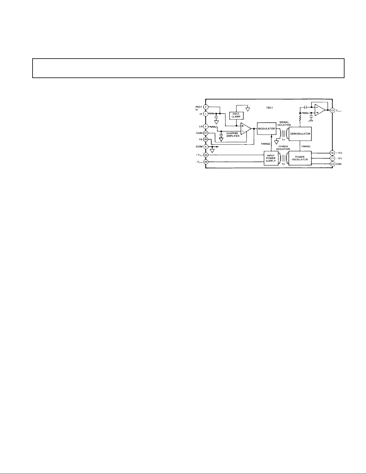
The 1B51 is a precision, mV/thermocouple signal conditioner
that incorporates a circuit design utilizing transformer based isolation and automated surface mount manufacturing technology.
It provides an unbeatable combination of versatility and performance in a compact plastic package. Designed for measurement
and control applications, it is specially suited for harsh environments with extremely high common-mode interference. Unlike
costlier solutions that require separate dc/dc converters, each
1B51 generates its own input side power, providing true, low
cost channel-to-channel isolation.
Functionally, the signal conditioner consists of three basic sections: chopper stabilized amplifier, isolation and output filter.
The chopper amplifier features a highly stable offset tempco of
±0.1 µV/°C and resistor programmable gains from 2 to 1000.
Wide range zero suppression can be implemented at this stage.
The isolation section has complete input to output galvanic isolation of 1500 V rms continuous using transformer coupling
techniques. Isolated power of 2 mA at ±6.2 V is provided for
ancillary circuits such as zero suppression and open-input detection. Filtering at 3 Hz is implemented by a passive antialiasing
filter at the front end and a two-pole active filter at the output.
= 3 Hz)
C
Signal Conditioner
1B51
FUNCTIONAL BLOCK DIAGRAM
Overall NMR is 60 dB and CMR is 160 dB min @ 60 Hz,
G = 1000.
The 1B51 is specified over –25°C to +85°C and operates over
the industrial (–40°C to +85°C) temperature range.
DESIGN FEATURES AND USER BENEFITS
High Noise Rejection: The combination of a chopper stabi-
lized front end with a low-pass filter provides high system accuracy in harsh industrial environments as well as excellent
rejection of 50 Hz/60 Hz noise.
Input Protection: The input is internally protected against
continuous application of 240 V rms.
Low Cost: The 1B51 offers a very low cost per channel for
high performance, isolated, low level signal conditioners.
Wide Range Zero Suppression: This input referred function
is a convenient way to null large input offsets.
Low-Pass Filter: The three pole active filter (f
reduces 60 Hz noise and aliasing errors.
Small Size: The 1B51 package size (1.0" × 2.1" × 0.35") and
functional completeness make it an excellent choice in systems
with limited board space and clearance.
= 3 Hz)
C
REV. A
Information furnished by Analog Devices is believed to be accurate and
reliable. However, no responsibility is assumed by Analog Devices for its
use, nor for any infringements of patents or other rights of third parties
which may result from its use. No license is granted by implication or
otherwise under any patent or patent rights of Analog Devices.
One Technology Way, P.O. Box 9106, Norwood, MA 02062-9106, U.S.A.
Tel: 617/329-4700 Fax: 617/326-8703
1B51–SPECIFICA TIONS
Model 1B51AN 1B51BN
GAIN
Gain Equation
Gain Error 1% max *
Gain Temperature Coefficient
Gain Nonlinearity ± 0.035% (± 0.05% max) ± 0.025% (±0.04% max)
OFFSET VOLTAGES
Input Offset Voltage
Initial, @ +25°C (Adjustable to Zero) 25 µV (100 µV max) *
vs. Temperature ±0.1 µV/°C (±0.5 µV/°C max) *
vs. Time, Noncumulative ±1 µV/month max *
Output Offset Voltage
Initial –50 mV –25 mV
vs. Temperature –175 µV/°C –50 µV/°C
INPUT OFFSET CURRENT
Initial 0.6 nA (2.5 nA max) *
vs. Temperature ±2.5 pA/°C (12.5 pA/°C max) *
INPUT BIAS CURRENT
Initial @ +25°C 10 nA *
vs. Temperature 10 pA/°C*
INPUT IMPEDANCE
Power On 50 MΩ *
Power Off 40 kΩ min *
INPUT VOLTAGE RANGE
Linear Differential Input ±10 mV to ± 5 V *
Max CMV, Input to Output
AC, 60 Hz, Continuous 1500 V rms *
Continuous, DC ±2000 V *
CMR @ 6 0 Hz, 1 kΩ Source Imbalance, G = 1000 160 dB min *
NMR @ 60 Hz 60 dB min *
Transient Protection IEEE-STD 472 (SWC) *
INPUT NOISE
Voltage, 0.1 Hz to 10 Hz, 1 kΩ Source Imbalance 1 µV p-p *
RATED OUTPUT
Voltage, 2 kΩ Load, min ±10 V *
Current ±5 mA *
Output Noise, DC to 100 kHz 1 mV p-p *
Impedance, DC 0.1 Ω *
FREQUENCY RESPONSE
Bandwidth, –3 dB dc to 3 Hz *
ISOLATED POWER
Voltage, No Load ±6.2 V ±5% *
Current 2 mA *
Regulation, No Load to Full Load 7.5% *
Ripple 250 mV p-p *
POWER SUPPLY
Voltage, Rated Performance ±15 V dc *
Voltage, Operating ± 13.5 V to ±18 V *
Current, Quiescent +12 mA @ +15 V, –4 mA @ –15 V *
PSRR 0.1%/V *
ENVIRONMENTAL
Temperature Range
Rated Performance –25° C to +85°C*
Operating –40°C to +85°C*
Storage –40°C to +85°C*
Relative Humidity 0 to 95%, @ +60°C*
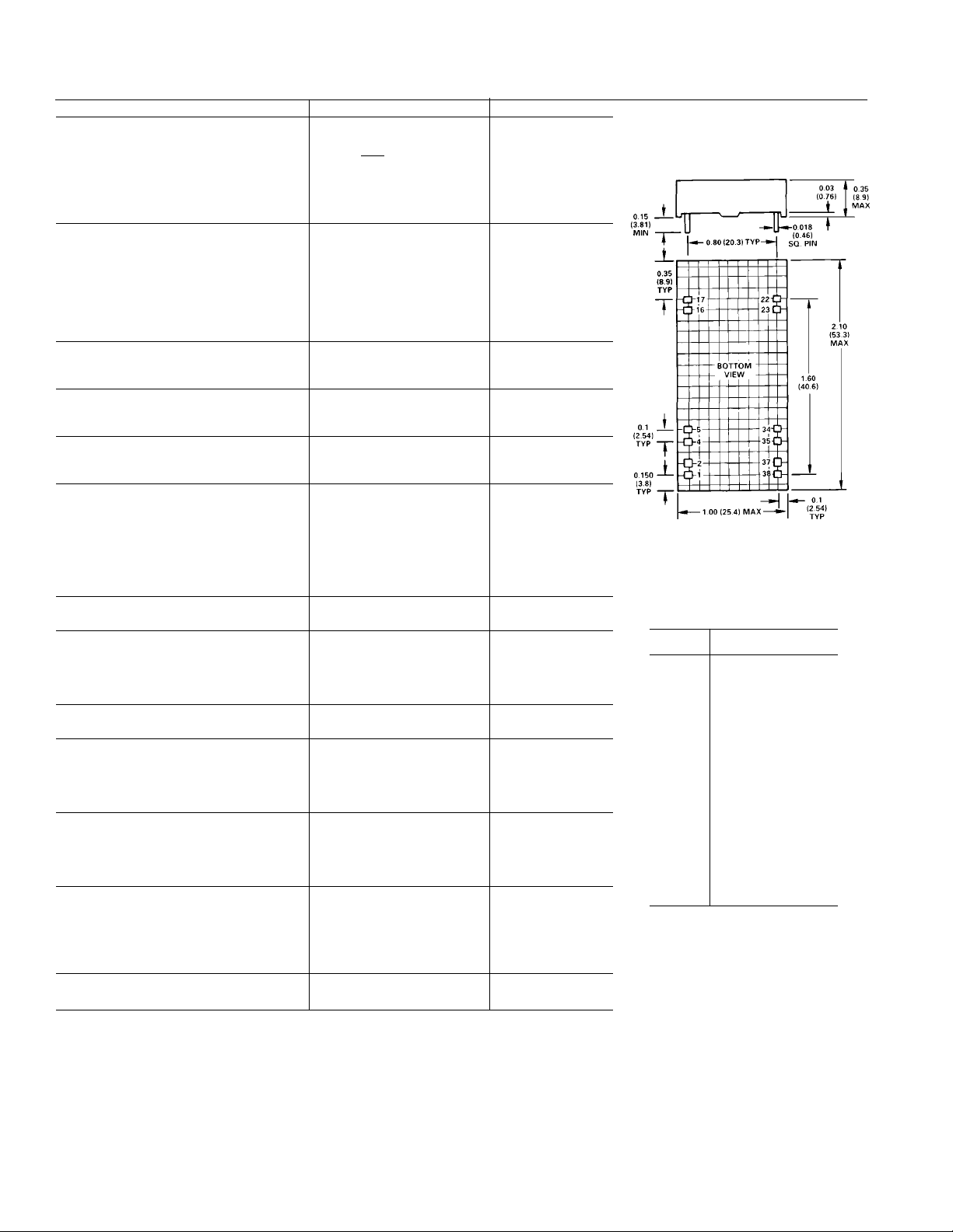
CASE SIZE 1.00" × 2.10" × 0.35" *
NOTES
•Specifications same as 1B51AN.
1
See graph in text.
Specifications subject to change without notice.
1
(typical at +258C and VS = 615 V unless otherwise noted)
R
G = 1+
50 ppm/°C*
(25.4 × 53.3 × 8.9) mm
FB
× 2
R
G
*
OUTLINE DIMENSIONS
Dimensions shown in inches and (mm).
PIN DESIGNATIONS
Pin Designation
11HI
12 PROT HI
14 ICOM
15LO
16 +15 V
17 –15 V
22 V
O
23 GND
34 –V
35 +V
ISO
ISO
37 GAIN
38 FB
–2–
REV. A

Functional Block Diagram
1B51
INSIDE THE 1B51
Referring to the functional block diagram, the ± 15 V power in-
puts provide power to both the output side circuitry and the
power oscillator. The 25 kHz power oscillator provides the tim-
ing information for the signal demodulator and drives power
transformer T2 for the input side power supplies. The second-
ary winding of T2 is half wave rectified and filtered to create the
input side bipolar unregulated supplies.
The signal input (HI) is single-pole filtered for noise rejection
and antialiasing. The protection clamps limit the voltage at
PROT HI to ±8 V. Thus, a large voltage applied between HI
and input common (ICOM) appears mostly across the input
resistor.
The chopper stabilized gain stage amplifies the differential input
voltage with a gain set by external resistors. The voltage at the
inverting input of the chopper stabilized amplifier (LO) should
be equal to the input voltage at which the desired output voltage
is zero. This is a true input referred zero suppression function.
The signal is amplitude modulated onto a 25 kHz carrier and
passed through the signal transformer T1. The synchronous de-
modulator restores the signal to the baseband. A two-pole active
low pass stage filters out clock noise and completes a three-pole
Butterworth filter formed with the input pole.
USING THE 1B51
Gain Setting
The gain of the 1B51 is controlled on the input side by a pair of
user provided resistors (see Figure 1). A feedback resistor of between 10 kΩ and 20 kΩ is required between the feedback pin
(FB) and the gain pin. The gain setting resistor is connected between the gain pin and input side common (ICOM). The gain
equation is
G = 1+
R
FB
×2
R
G
Gains of 2–1000 can be achieved by adjusting this ratio.
The accuracy of the resistor values must be taken into account
when calculating the initial gain accuracy of an application. The
initial accuracy of the 1B51 must then be added to the resistor
errors to predict the total accuracy. Likewise, the ratiometric
temperature coefficient of the gain and feedback resistors must
be added to the temperature coefficient of the 1B51 to predict
the total resulting thermal drift.
It is possible to use a trimming potentiometer to correct for initial gain and system gain errors. The feedback resistor can be
comprised of a resistor in series with a trimming potentiometer,
as long as the total resistance remains between 10 kΩ and
20 kΩ. Alternatively, the gain resistor can also be an adjustable
resistor. In general, the greater the trim range, the coarser the
resolution.
Zero Suppression
Since the 1B51 is a differential input device, true input referred
zero suppression can be accomplished (see Figure 1). A voltage
reference powered by the input side power supplies is applied to
the LO terminal. Since the transfer function is
VO=(V(HI )–V(LO))×GAIN
the input voltage for which the desired output is zero should be
applied to the LO pin. The equation is
Figure 1. Input Gain Setting and Zero Suppression
REV. A
VZ=1.25(R2/(R1+ R2))
Any drift of this input zero suppression voltage appears as offset
drift, so a temperature stable reference should be used. The
source impedance at the LO terminal should be kept below 1 kΩ.
–3–

1B51
Open Input Detection
The 1B51 can sense an open thermocouple or broken input
line with the addition of an external resistor. By connecting a
220 MΩ resistor between the HI pin and the positive or negative isolated supply, an open input will cause a positive or negative full-scale output, respectively.
To preserve the normal mode input protection capability of the
1B51, the resistor must be able to withstand 220 V ac. A high
voltage rating can be obtained by connecting lower value resistors in series.
Cold Junction Compensation
When using a thermocouple as an input to the 1B51, a second
thermocouple junction is formed at the terminations of the thermocouple wires, commonly referred to as the cold junction. The
measured output voltage of the sensor is the voltage generated
by the thermocouple minus the voltage generated by the cold
junction.
Since thermocouples are specified with 0 V representing 0°C, it
would be ideal to maintain the cold junction at 0°C. A more
practical approach involves adding a temperature dependent
voltage to the thermocouple signal so as to oppose the cold
junction effects. This type of correction is known as cold junction compensation.
Many different methods are commonly used to implement cold
junction compensation. Usually a thermistor or a semiconductor
sensor is used to generate the cold junction voltage. The slope
of the cold junction voltage must be the same as that of the thermocouple. Therefore, the cold junction compensation depends
on the thermocouple type.
Sometimes, one cold junction compensation sensor is used by a
number of thermocouple channels. This is accomplished by
measuring the temperature of the connection block directly, and
adding the appropriate voltage to each uncompensated thermocouple channel after the gain has been taken. In all cases, the cold
junction sensor must be in the thermal proximity with the connection
block.
Figure 2 shows a monolithic cold junction compensation device
used with the 1B51. The Analog Devices AC1226 measures the
ambient temperature and generates the appropriate cold junction voltage for several different thermocouple types.
Figure 2. 1B51 Cold Junction Compensation
C1147–10–1/89
TYPICAL PERFORMANCE CURVES
Gain vs. Temperature
(@TA = +258C, VS = 615 V)
CMR vs. Gain
PRINTED IN U.S.A.
+V
Ripple vs. Capacitance
Iso
–4–
+V
Iso
vs. Load
REV. A
 Loading...