

Programmable Controller for
www.BDTIC.com/ADI
FEATURES
Programmable capacitance-to-digital converter
25 ms update rate (@ maximum sequence length)
Better than 1 fF resolution
8 capacitance sensor input channels
No external RC tuning components required
Automatic conversion sequencer
On-chip automatic calibration logic
Automatic compensation for environmental changes
Automatic adaptive threshold and sensitivity levels
On-chip RAM to store calibration data
2
I
C®-compatible serial interface
Separate VDRIVE level for serial interface
Interrupt output for host controller
16-lead, 4 mm x 4 mm LFCSP-VQ
2.6 V to 3.6 V supply voltage
Low operating current
Full power mode: less than 1 mA
Low power mode: 50 µA
Capacitance Touch Sensors
AD7143
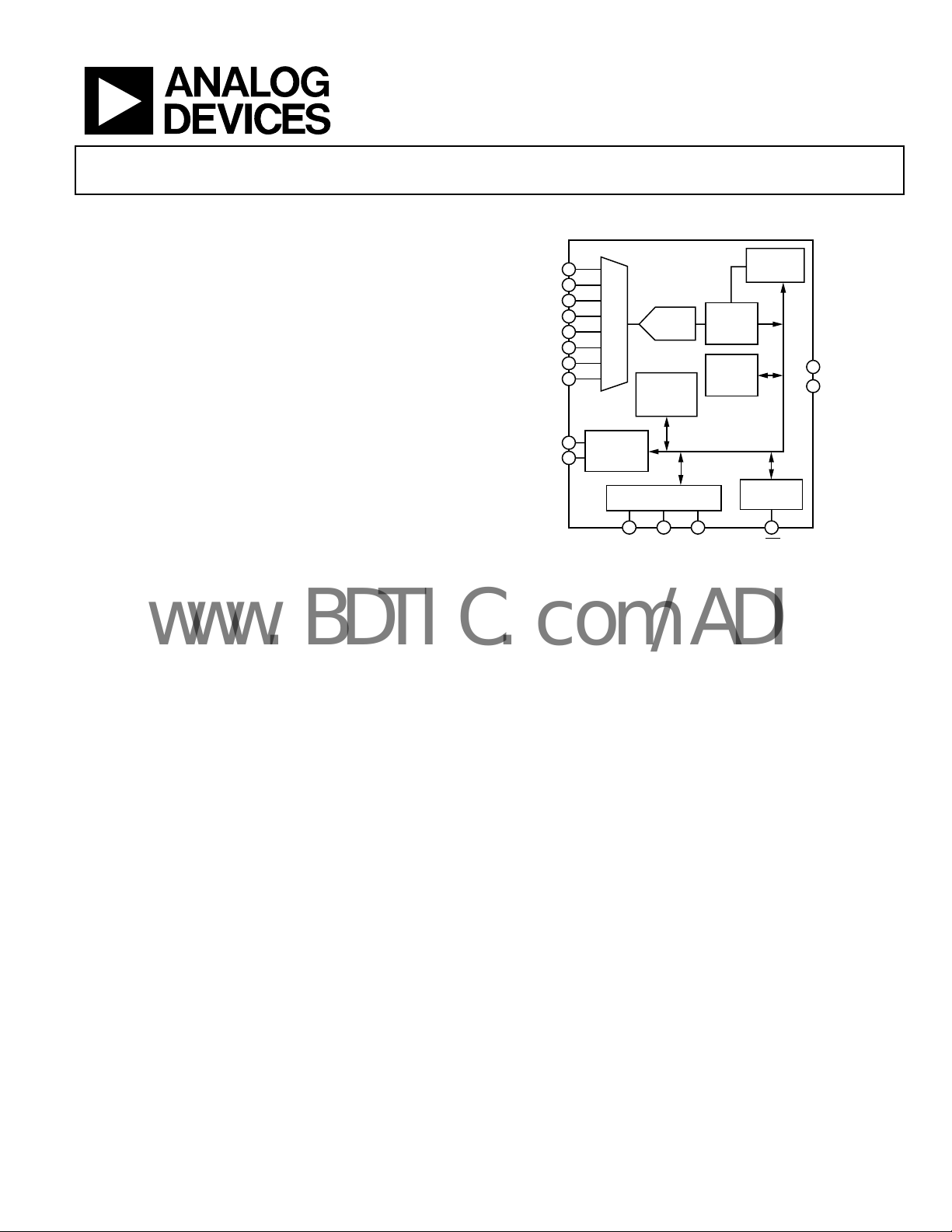
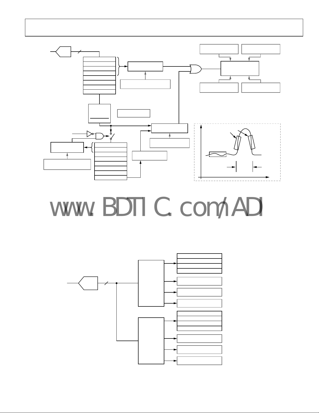
FUNCTIONAL BLOCK DIAGRAM
POWER-ON
TION
ENGINE
TION
RAM
RESET
LOGIC
INTERRUPT
LOGIC
9
VCC
10
GND
CIN0
CIN1
CIN2
CIN3
CIN4
CIN5
CIN6
CIN7
CSHIELD
SRC
15
16
1
2
3
4
5
6
7
8
MATRIX
SWITCH
CONTROL
DATA
REGISTERS
250kHz
EXCITATION
SOURCE
2
I
C SERIAL INT ERFACE
AND CONTROL L OGIC
SDA SCLK INT
VDRIVE
AD7143
16-BIT
Σ-Δ
CDC
AND
Figure 1.
CALIBRA-
CALIBRA-
13 141211
06472-001
APPLICATIONS
Personal music and multimedia players
Cell phones
Digital still cameras
Smart hand-held devices
Television, A/V, and remote controls
Gaming consoles
GENERAL DESCRIPTION
The AD7143 is an integrated capacitance-to-digital converter
(CDC) with on-chip environmental calibration for use in
systems requiring a novel user input method. The AD7143
interfaces to external capacitance sensors implementing
functions, such as capacitive buttons, scroll bars, and
scroll wheels.
The CDC has eight inputs channeled through a switch matrix to
a 16-b
it, 250 kHz sigma-delta (∑-∆) capacitance-to-digital
converter. The CDC is capable of sensing changes in the
capacitance of the external sensors and uses this information to
register a sensor activation. The external sensors can be
arranged as a series of buttons, as a scroll bar or wheel, or as a
combination of sensor types. By programming the registers, the
user has full control over the CDC setup. High resolution
sensors require software to run on the host processor.
The AD7143 has on-chip calibration logic to account for
changes in the ambient environment. The calibration sequence is
performed automatically and at continuous intervals, while the
sensors are not touched. This ensures that there are no false or
nonregistering touches on the external sensors due to a
changing environment.
2
The AD7143 has an I
separate VDRIVE pin for I
C-compatible serial interface and a
2
C serial interface operating voltages
between 1.65 V and 3.6 V.
The AD7143 is available in a 16-lead, 4 mm × 4 mm LFCSP-VQ
nd operates from a 2.6 V to 3.6 V supply. The operating
a
current consumption is less than 1 mA, falling to 50 µA in low
power mode (conversion interval of 400 ms).
Rev. 0
Information furnished by Analog Devices is believed to be accurate and reliable. However, no
responsibility is assumed by Anal og Devices for its use, nor for any infringements of patents or ot her
rights of third parties that may result from its use. Specifications subject to change without notice. No
license is granted by implication or otherwise under any patent or patent rights of Analog Devices.
Trademarks and registered trademarks are the property of their respective owners.
One Technology Way, P.O. Box 9106, Norwood, MA 02062-9106, U.S.A.
Tel: 781.329.4700 www.analog.com
Fax: 781.461.3113 ©2007 Analog Devices, Inc. All rights reserved.

AD7143
www.BDTIC.com/ADI
TABLE OF CONTENTS
Features .............................................................................................. 1
Proximity Sensitivity.................................................................. 17
Applications....................................................................................... 1
Functional Block Diagram .............................................................. 1
General Description......................................................................... 1
Revision History ............................................................................... 2
Specifications..................................................................................... 3
2
I
C Timing Specifications............................................................ 5
Absolute Maximum Ratings............................................................ 6
ESD Caution.................................................................................. 6
Pin Configurations and Function Descriptions ........................... 7
Typical Performance Characteristics ............................................. 8
Theory of Operation ...................................................................... 11
Capacitance Sensing Theory ..................................................... 11
Operating Modes........................................................................ 12
Capacitance Sensor Input Configuration.................................... 13
CIN Input Multiplexer Setup.................................................... 13
Slow FIFO.................................................................................... 19
SLOW_FILTER_UPDATE_LVL.............................................. 19
Environmental Calibration........................................................... 22
Capacitance Sensor Behavior without Calibration ................ 22
Capacitance Sensor Behavior with Calibration...................... 23
Adaptive Threshold and Sensitivity............................................. 25
Interrupt Output............................................................................. 26
CDC Conversion Complete Interrupt..................................... 26
Sensor Touch Interrupt.............................................................. 26
Serial Interface................................................................................ 28
2
I
C Compatible Interface........................................................... 28
PCB Design Guidelines ................................................................. 31
Capacitive Sensor Board Mechanical Specifications............. 31
Chip Scale Packages ................................................................... 31
Power-Up Sequence ....................................................................... 32
Capacitiance-to-Digital Converter............................................... 14
Oversampling the CDC Output ............................................... 14
Capacitance Sensor Offset Control .......................................... 14
Conversion Sequencer ............................................................... 14
CDC Conversion Sequence Time ............................................ 15
CDC Conversion Results........................................................... 16
Noncontact Proximity Detection .................................................17
Recalibration ............................................................................... 17
REVISION HISTORY
1/07—Revision 0: Initial Version
Typical Applicat i o n C i rc uits ......................................................... 33
Register Map ................................................................................... 34
Detailed Register Descriptions..................................................... 35
Bank 1 Registers ......................................................................... 35
Bank 2 Registers ......................................................................... 43
Bank 3 Registers ......................................................................... 47
Outline Dimensions ....................................................................... 55
Ordering Guide .......................................................................... 55
Rev. 0 | Page 2 of 56
AD7143
www.BDTIC.com/ADI
SPECIFICATIONS
VCC = 2.6 V to 3.6 V, TA = −40oC to +85°C, unless otherwise noted.
Table 1.
Parameter Min Typ Max Unit Test Conditions/Comments
CAPACITANCE-TO-DIGITAL CONVERTER
Update Rate 23 25 26 ms Eight conversion stages in sequencer, decimation = 256
Resolution 16 Bit
CIN Input Range
1
±2 pF
No Missing Codes 16 Bit
CIN Input Leakage 25 nA
Total Unadjusted Error ±20 %
Output Noise (Peak-to-Peak) 7 Codes
3 Codes
Output Noise (RMS) 0.8 Codes
0.5 Codes
Parasitic Capacitance 40 pF
Offset Range
C
BULK
C
Offset Resolution 156.25 fF
BULK
1
±20 pF
Low Power Mode Delay Accuracy 5 %
EXCITATION SOURCE
Frequency 237.5 240 262.5 kHz
Output Voltage VCC V
Short-Circuit Source Current 20 mA
Short-Circuit Sink Current 50 mA
Maximum Output Load 250 pF
C
Output Drive 10 μA
SHIELD
C
Bias Level VCC/2 V
SHIELD
LOGIC INPUTS (SCLK, SDA)
V
Input High Voltage 0.7 × V
IH
V
Input Low Voltage 0.4 V
IL
I
Input High Voltage −1 μA
IH
I
Input Low Voltage 1 μA VIN = GND
IL
DRIVE
V
Hysteresis 150 mV
OPEN-DRAIN OUTPUTS (S
CLK, SDA, INT)
VOL Output Low Voltage 0.4 V I
I
Output High Leakage Current +0.1 ±1 μA
OH
POWER
V
V
I
CC
DRIVE
CC
2.6 3.3 3.6 V
1.65 3.6 V
0.9 1 mA In full power mode
20 μA
16 30 μA
4.5 μA
2.25 15 μA Full shutdo
1
C
and C
IN
PLASTIC O VERLAY
are defined as follows:
BULK
SENSOR BOARD
CAPACITIVE SENSO R
C
C
IN
BULK
05702-054
Guaranteed by design, but not production tested
Decimation rate = 128
Decimation rate = 256
Decimation rate = 128
Decimation rate = 256
Parasitic capacitance to ground, per CIN input guaranteed
by characterization
% of 200 ms, 400 ms, 600 ms, or 800 ms
Capacitance load on source to ground
= −1 mA
SINK
Low power mode, converter idle, TA = 25°C
Low power mode, converter idle
Full shutdown, TA = 25°C
wn
Rev. 0 | Page 3 of 56
AD7143
www.BDTIC.com/ADI
Table 2. Typical Average Current in Low Power Mode, VCC = 3.6 V, T = 25°C, Load of 50 pF on SRC Pin
Number of Conversion Stages, Current Values Expressed in A
Low Power Mode Delay Decimation Rate
200 ms 128 26.4 33.3 40.1 46.9 53.5 60 66.5 72.8
256 35.6 49.1 62.2 74.9 87.3 99.3 111 122.3
400 ms 128 21.3 24.8 28.3 31.7 35.2 38.6 42 45.4
256 26 32.9 39.7 46.5 53.1 59.6 66.1 72.4
600 ms 128 19.6 21.9 24.3 26.6 28.9 31.2 33.5 35.8
256 22.7 27.4 32 25.6 41.1 45.6 50 54.4
800 ms 128 18.7 20.5 22.2 24 25.7 27.5 29.2 31
256 21.1 24.6 28.1 31.5 35 38.4 41.8 45.2
Table 3. Maximum Average Current in Low Power Mode, VCC = 3.6 V, Load of 50 pF on SRC Pin
Low Power Mode Delay Decimation Rate
200 ms 128 42.2 50.5 58.7 66.7 74.6 82.3 90.0 97.5
256 53.2 69.3 84.9 100.0 114.6 128.7 142.5 155.8
400 ms 128 36.1 40.4 44.5 48.7 52.8 56.9 60.9 64.5
256 41.8 50.1 58.2 66.2 74.1 82.0 89.5 97.1
600 ms 128 34.1 37.0 39.7 42.5 45.3 48.1 50.8 53.4
256 37.9 43.5 49.0 54.5 60.0 65.2 70.5 75.7
800 ms 128 33.1 35.2 37.3 39.4 41.5 43.6 45.7 47.7
256 35.9 40.1 44.3 48.4 52.6 56.6 60.7 64.7
1 2 3 4 5 6 7 8
Number of Conversion Stages, Current Values Expressed in A
1 2 3 4 5 6 7 8
Rev. 0 | Page 4 of 56
AD7143
www.BDTIC.com/ADI
I2C TIMING SPECIFICATIONS
TA = −40°C to +85°C, VCC = 2.6 V to 3.6 V, unless otherwise noted. Sample tested at 25°C to ensure compliance. All input signals timed
from a voltage level of 1.6 V.
Table 4. I
2
C Timing Specifications
1
Parameter Limit Unit Description
f
t
t
t
t
t
t
t
t
SCLK
1
2
3
4
5
6
7
8
400 kHz max
0.6 μs min Start condition hold time, t
1.3 μs min Clock low period, t
0.6 μs min Clock high period, t
100 ns min Data setup time, t
300 ns min Data hold time, t
SU; DAT
HD; DAT
0.6 μs min Stop condition setup time, t
0.6 μs min Start condition setup time, t
1.3 μs min Bus free time between stop and start conditions, t
tR 300 ns max Clock/data rise time
t
300 ns max Clock/data fall time
F
1
Guaranteed by design, not production tested.
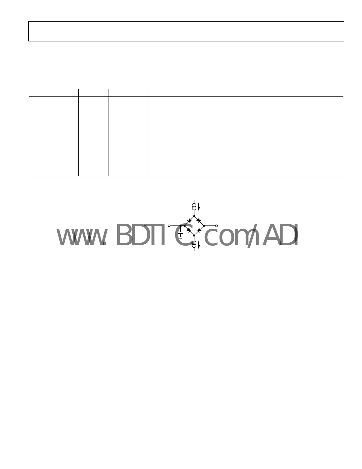
200µA I
TO OUTPUT
PIN
C
L
50pF
200µA I
Figure 2. Load Circuit for Digital Out
HD; STA
LOW
HIGH
SU; STO
SU; STA
OL
1.6V
OH
put Timing Specifications
06472-003
BUF
Rev. 0 | Page 5 of 56
AD7143
www.BDTIC.com/ADI
ABSOLUTE MAXIMUM RATINGS
Parameter Rating
VCC to GND −0.3 V to +3.6 V
Analog Input Voltage to GND −0.3 V to VCC + 0.3 V
Digital Input Voltage to GND −0.3 V to VDRIVE + 0.3 V
Digital Output Voltage to GND −0.3 V to VDRIVE + 0.3 V
Input Current to Any Pin Except
Supplies
ESD Rating (Human Body Model) 2.5 kV
Operating Temperature Range −40°C to +150°C
Storage Temperature Range −65°C to +150°C
Junction Temperature 150°C
LFCSP_VQ
Power Dissipation 450 mW
θJA Thermal Impedance 135.7°C/W
IR Reflow Peak Temperature 260°C (±0.5°C)
Lead Temperature (Soldering 10 sec) 300°C
1
Transient currents of up to 100 mA do not cause SCR latch-up.
1
10 mA
Stresses above those listed under Absolute Maximum Ratings
ma
y cause permanent damage to the device. This is a stress
rating only; functional operation of the device at these or any
other conditions above those indicated in the operational
section of this specification is not implied. Exposure to absolute
maximum rating conditions for extended periods may affect
device reliability.
ESD CAUTION
Rev. 0 | Page 6 of 56
AD7143
www.BDTIC.com/ADI
PIN CONFIGURATIONS AND FUNCTION DESCRIPTIONS
CIN0
CIN1
INT
SCLK
14
13
15
16
PIN 1
INDICATO R
1CIN2
2CIN3
AD7143
3CIN4
TOP VIEW
(Not to Scale)
4CIN5
5
6
CIN6
CIN7
Figure 3. Pin Configuration
Table 5. Pin Function Descriptions
Pin No. Mnemonic Description
1 CIN2 Capacitance Sensor Input.
2 CIN3 Capacitance Sensor Input.
3 CIN4 Capacitance Sensor Input.
4 CIN5 Capacitance Sensor Input.
5 CIN6 Capacitance Sensor Input.
6 CIN7 Capacitance Sensor Input.
7 CSHIELD CDC Shield Potential Output. Requires 10 nF capacitor to ground.
8 SRC CDC Excitation Source Output.
9 VCC CDC Supply Voltage.
10 GND Ground Reference Point for All CDC Circuitry. Tie to ground plane.
11 VDRIVE I2C Serial Interface Operating Voltage
12 SDA I2C Serial Data Input/Output. SDA requires pull-up resistor.
13 SCLK Clock Input for Serial Interface. SCLK requires pull-up resistor.
14
INT
General-Purpose Open-Drain Interrupt Output. Programmable polarity; requires pull-up resistor.
15 CIN0 Capacitance Sensor Input.
16 CIN1 Capacitance Sensor Input.
12 SDA
11 VDRIVE
10 GND
9VCC
8
7
SRC
CSHIELD
06472-004
Rev. 0 | Page 7 of 56

AD7143
www.BDTIC.com/ADI
TYPICAL PERFORMANCE CHARACTERISTICS
1000
980
960
940
920
(µA)
I
DEVICE 2
CC
900
880
860
840
820
2.7 2. 92. 8 3.0 3.1 3.2 3.3 3.4 3. 5 3.6
DEVICE 3
DEVICE 1
VCC(V)
Figure 4. Supply Current vs. Supply Voltage
06472-005
2.45
2.30
2.15
(µA)
CC
2.00
1.85
SHUTDOWN I
1.70
1.55
1.40
2.7 2. 92.8 3.03.13.23.33.43.53.6
DEVICE 1
VCC (V)
Figure 7. Shutdown Supply Cu
DEVICE 2
DEVICE 3
rrent vs. Supply Voltage
06472-008
180
160
140
120
(µA)
CC
I
100
80
LP_CONV_DEL AY = 600ms
60
40
2.72.82.93.03.13.2 3.43.3 3.5 3.6
LP_CONV_DEL AY = 200ms
LP_CONV_DELAY = 400ms
LP_CONV_DELAY = 800ms
VCC(V)
Figure 5. Low Power Supply Current vs. Supply Voltage,
Decimation Rate = 256
120
100
80
(µA)
CC
I
60
40
20
LP_CONV_DEL AY = 200ms
LP_CONV_DEL AY = 400ms
LP_CONV_DEL AY = 600ms
LP_CONV_DEL AY = 800ms
2.7 2.8 2.9 3.0 3.1 3.2 3.43.3 3. 5 3.6
VCC(V)
Figure 6. Low Power Supply Current vs. Supply Voltage
Deci
mation Rate = 128
1.10
DEVICE 1
1.05
1.00
(mA)
0.95
CC
I
DEVICE 3
0.90
0.85
06472-006
0.80
0 50 100 150 200 250 300 350 400 450 500
CAPACITANCE LOAD O N SOURCE (pF )
DEVICE 2
06472-009
Figure 8. Supply Current vs. Capacitive Load on SRC
16015
16010
16005
16000
15995
CDC OUTPUT CODE
15990
15985
06472-007
15980
DEVICE 1
DEVICE 2
DEVICE 3
0 50 100 150 200 250 300 350 400 450 500
CAPACITANCE LO AD ON SOURCE (pF )
06472-010
Figure 9. Output Code vs. Capacitive Load on SRC
Rev. 0 | Page 8 of 56
AD7143
www.BDTIC.com/ADI
960
940
920
900
880
860
840
SUPPLY CURRENT (µA)
820
800
780
–40 120100
TEMPERATURE ( °C)
Figure 10. Supply Current vs. Temperature
12
10
8
6
4
SUPPLY CURRENT (µA)
2
0
–40 120100806040
200–20
TEMPERATURE (°C)
Figure 11. Shutdown Supply Cu
3.3V
rrent vs. Temperature
3.6V
3.3V
2.7V
3.6V
806040200–20
06472-011
2.7V
06472-012
0.020
0.015
0.010
0.005
ERROR (pF)
0
–0.005
–0.010
0 70k
10k 20k 30k 40k 50k 60k
CDC OUTPUT CODE
CDC OUTPUT CODE
Figure 13. 3.3 V Linearity Error
2.5
2.0
1.5
1.0
0.5
CDC PEAK-TO-PEAK NOISE (Codes)
0
10 10M100k1k
Figure 14. Power Supply Si
100mV
200mV
FREQUENCY (Hz)
ne Wave Rejection
300mV
400mV
500mV
06472-046
06472-013
4.8
4.3
3.8
3.3
2.8
CAPACITANCE (pF )
2.3
1.8
1.3
0 10k 20k 30k 40k 50k 60k
CDC OUTPUT CODE
CDC OUTPUT CODE
Figure 12. 3.3 V Linearity
06472-045
Rev. 0 | Page 9 of 56
180
160
140
120
100
80
60
40
CDC PEAK-TO-PEAK NOISE (Codes)
20
0
100 10M
SQUARE WAVE F REQUENCY (Hz)
Figure 15. Power Supply Square Wave Rejection
1M10k 100k1k
300mV
200mV
100mV
50mV
25mV
06472-014

AD7143
www.BDTIC.com/ADI
32900
32800
32700
32600
32500
32400
32300
32200
CDC OUTPUT CODE (D)
32100
32000
31900
06
Figure 16. CDC Output Codes vs. Parasitic Capacitance
PARASITIC
CAPACITANCE
10 20 30 40 50
PCB PARASITIC CAPACI TANCE (pF )
06472-047
0
Rev. 0 | Page 10 of 56
AD7143
R
www.BDTIC.com/ADI
THEORY OF OPERATION
The AD7143 is a capacitance-to-digital converter (CDC) with
on-chip environmental compensation, intended for use in
portable systems requiring high resolution user input. The
internal circuitry consists of a 16-bit, ∑-∆ converter that
converts a capacitive input signal into a digital value. There are
eight input pins, CIN0 to CIN7, on the AD7143. A switch
matrix routes the input signals to the CDC. The result of each
capacitance-to-digital conversion is stored in on-chip registers.
The host subsequently reads the results over the serial interface.
The AD7143 has an I
compatible with a wide range of host processors.
The AD7143 interfaces with up to eight external capacitance
ensors. These sensors can be arranged as buttons, scroll bars,
s
wheels, or as a combination of sensor types. The external
sensors consist of electrodes on a single or multiple layer PCB
that interface directly to the AD7143.
The AD7143 can be set up to implement any set of input
ensors by programming the on-chip registers. The registers can
s
also be programmed to control features such as averaging,
offsets, and gains for each of the external sensors. There is a
sequencer on-chip to control how each of the capacitance
inputs is polled.
2
C interface, ensuring that the parts are
The AD7143 operates from a 2.6 V to 3.6 V supply, and is
a
vailable in a 16-lead, 4 mm × 4 mm LFCSP_VQ.
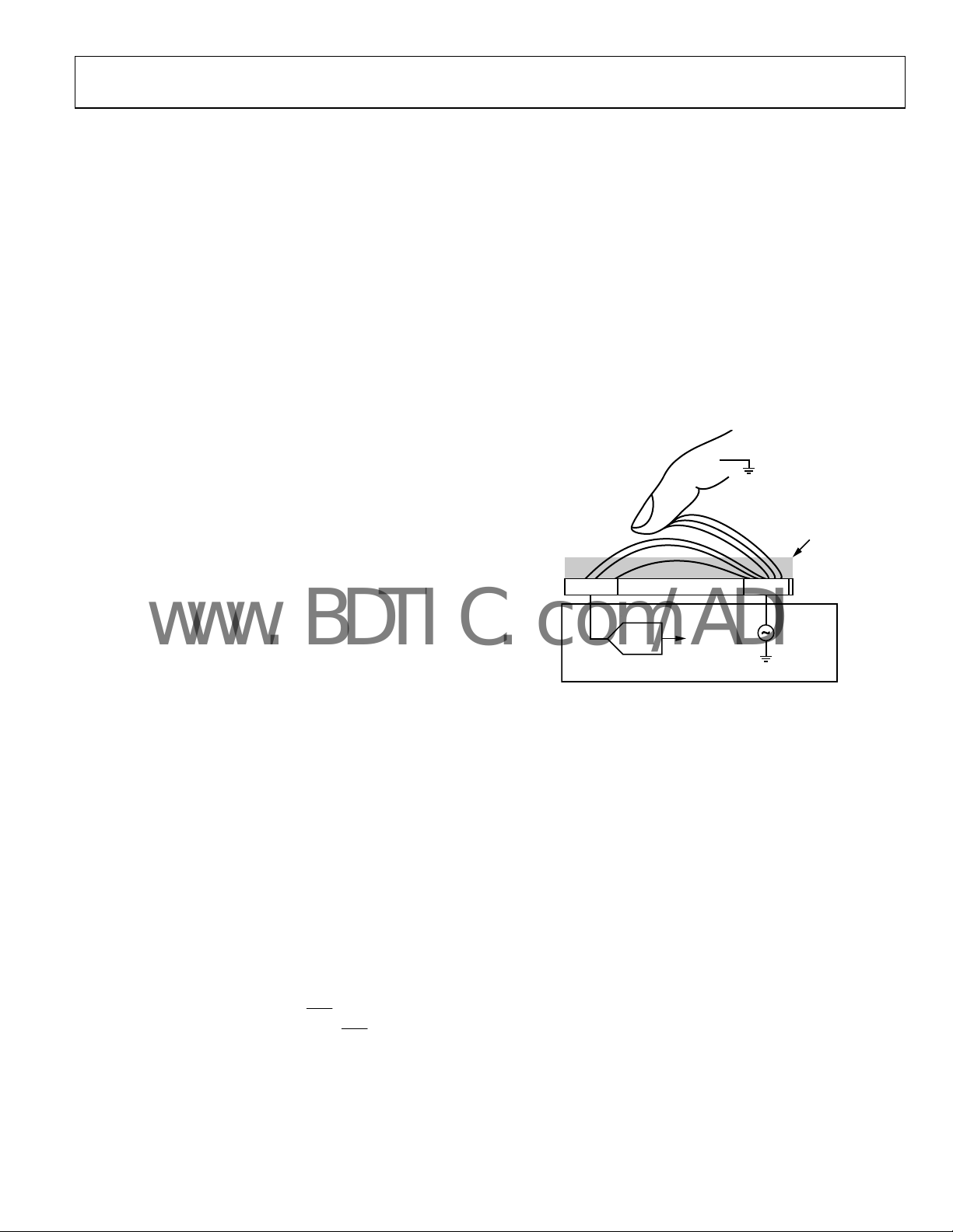
CAPACITANCE SENSING THEORY
The AD7143 uses a method of sensing capacitance known as
the shunt method. Using this method, an excitation source is
connected to a transmitter generating an electric field to a
receiver. The field lines measured at the receiver are translated
into the digital domain by a ∑-∆ converter. When a finger, or
other grounded object, interferes with the electric field, some of
the field lines are shunted to ground and do not reach the
receiver (see
m
easured at the receiver decreases when an object comes close
to the induced field.
Figure 17). Therefore, the total capacitance
PLAST IC COVE
TxRx PCB L AYER
The AD7143 has on-chip digital logic and 528 words of RAM
used
for environmental compensation. The effects of humidity,
temperature, and other environmental factors can effect the
operation of capacitance sensors. Transparent to the user, the
AD7143 performs continuous calibration to compensate for
these effects, allowing the AD7143 to give error-free results at
all times.
The AD7143 requires some minor companion software that
uns on the host or other microcontroller to implement high
r
resolution sensor functions, such as a scroll bar or wheel.
However, no host software is required to implement buttons,
including 8-way button functionality. Button sensors are
implemented completely in digital logic on-chip with the status
of each button reported in interrupt status registers.
The AD7143 can be programmed to operate in either full power
de, or in low power automatic wake-up mode. The
mo
automatic wake-up mode is particularly suited for portable
devices that require low power operation giving the user
significant power savings coupled with full functionality.
INT
The AD7143 has an interrupt output,
new data has been placed into the registers.
interrupt the host on sensor activation.
, to indicate when
INT
is used to
16-BIT
DATA
Σ-Δ
ADC
AD7143
Figure 17. Single Layer Sensing Capacitance Method
In practice, the excitation source and ∑-∆ ADC are implemented
on the AD7143, while the transmitter and receiver are constructed
on a PCB that comprises the external sensor.
EXCITATIO N
SIGNAL
250kHz
06472-015
Registering a Sensor Activation
When a sensor is approached, the total capacitance associated
with that sensor, measured by the AD7143, changes. When the
capacitance changes to such an extent that a set threshold is
exceeded, the AD7143 registers this as a sensor touch and then
automatically updates the internal interrupt status registers.
Preprogrammed threshold levels are used to determine if a
nge in capacitance is due to a button being activated. If the
cha
capacitance exceeds one of the threshold limits, the AD7143
registers this as a true button activation. The same threshold
principle is used to determine if other types of sensors, such as
sliders or scroll wheels, are activated.
Rev. 0 | Page 11 of 56

AD7143
www.BDTIC.com/ADI
Complete Solution for Capacitance Sensing
Analog Devices, Inc. provides a complete solution for
capacitance sensing. The two main elements to the solution are
the sensor PCB and the AD7143.
If the application requires high resolution sensors, such as scroll
rs or wheels, software is required that runs on the host
ba
processor. (No software is required for button sensors.) The
memory requirements for the host depend upon the sensor, and
are typically 9 kB of code and 600 bytes of data memory.
SENSOR PCB
S1
S2
S3
S4
S5
S6
S7
S8
8
AD7143
SRC
I2C
HOST PROCESSOR
1 MIPS
9kB ROM
600 BYTES RAM
Full Power Mode
In full power mode, all sections of the AD7143 remain fully
powered at all times. While a sensor is being touched, the
AD7143 processes the sensor data. If no sensor is touched, the
AD7143 measures the ambient capacitance level and uses this
data for the on-chip compensation routines. In full power
mode, the AD7143 converts at a constant rate. See the
onversion Sequence Time section for more information.
C
CDC
Low Power Mode
When in low power mode, the AD7143 POWER_MODE bits
are set to 10 upon device initialization. If the external sensors
are not touched, the AD7143 reduces its conversion frequency,
thereby greatly reducing its power consumption. The part
remains in a reduced power state when the sensors are not
touched. Every LP_CONV_DELAY ms (200 ms, 400 ms, 600
ms or 800 ms), the AD7143 performs a conversion and uses this
data to update the compensation logic. When an external
sensor is touched, the AD7143 begins a conversion sequence
every 25 ms to read back data from the sensors.
06472-016
Figure 18. Three Part Capacitance Sensing Solution
Analog Devices supplies the sensor PCB footprint design
libraries to the customer based on the customer’s specifications,
and supplies any necessary software on an open-source basis.
OPERATING MODES
The AD7143 has three operating modes. Full power mode,
where the device is always fully powered, is suited for applications
where power is not a concern. One example is game consoles
that have an ac power supply. Low power mode, where the part
automatically powers down, is tailored to give significant power
savings over full power mode, and is suited for mobile applications
where power must be conserved. In shutdown mode, the part
shuts down completely.
The POWER_MODE bits (Bit 0 and Bit 1) of the control
r
egister set the operating mode on the AD7143. The control
register is at Address 0x000. Table 6 shows the POWER_MODE
s
ettings for each operating mode. To put the AD7143 into
shutdown mode, set the POWER_MODE bits to either 01 or 11.
Table 6. POWER_MODE Settings
POWER_MODE Bits Operating Mode
00 Full power mode
01 Full shutdown mode
10 Low power mode
11 Full shutdown mode
The power-on default setting of the POWER_MODE bits is 00,
full power mode.
In low power mode, the total current consumption of the
AD7143 is a
n average of the current used during a conversion,
and the current used while the AD7143 is waiting for the next
conversion to begin. For example, when LP_CONV_DELAY is
400 ms, the AD7143 typically uses 0.9 mA current for 25 ms
and 15 A for 400 ms of the conversion interval. Note that these
conversion timings can be altered through the register settings.
See the
CDC Conversion Sequence Time section for more
rmation.
info
AD7143 SETUP
AND INITIALIZATION
POWER_MO DE = 10
ANY
NO YES
SENSOR
TOUCHED?
CONVERSIO N SEQUENCE
EVERY LP_CONV_DELAY m s
UPDATE COMPENSATIO N
LOGIC DATA PATH
Figure 19. Low Power Mode Operation
CONVERSION SE QUENCE
EVERY 25ms FOR
SENSOR READ BACK
YES
ANY SENSOR
TOUCHED?
NO
PROXIMITY TIMER
COUNT DO WN
TIMEOUT
The time taken for the AD7143 to go from a full power state to
a reduced power state, once the user stops touching the external
sensors, is configurable. Once the sensors are not touched, the
PWR_DWN_TIMEOUT bits, in the Ambient Compensation
Ctrl 0 Register at Address 0x002, control the amount of time
necessary for the device to return to a reduced power state.
06472-017
Rev. 0 | Page 12 of 56

AD7143
www.BDTIC.com/ADI
CAPACITANCE SENSOR INPUT CONFIGURATION
Each input connection from the external capacitance sensors to
the AD7143 converter can be uniquely configured by using the
registers in Tabl e 38 and Ta ble 3 9. These registers are used to
c
onfigure input pin connection setups, sensor offsets, sensor
sensitivities, and sensor limits for each stage. Each sensor can be
individually optimized. For example, a button sensor connected
to STAGE0 can have a different sensitivity and offset values
than a button with a different function that is connected to a
different stage.
CIN INPUT MULTIPLEXER SETUP
The CIN_CONNECTION_SETUP registers in Tabl e 38 list the
available options for connecting the sensor input pin to the CDC.
CIN CONNECTIO N SETUP BIT S CIN SETTING
The AD7143 has an on-chip multiplexer to route the input
nals from each pin to the input of the converter. Each input
sig
pin can be tied to either the negative or the positive input of the
CDC or can be left floating. Each input can also be internally
connected to the C
an input is not used, always connect it to C
signal to help prevent cross coupling. If
SHIELD
.
SHIELD
Connecting a CINx input pin to the positive CDC input results
decrease in CDC output code when the corresponding
in a
sensor is activated. Connecting a CINx input pin to the negative
CDC input results in an increase in CDC output code when the
corresponding sensor is activated.
Two bits in each sequencer stage register control the mux
tting for the input pin.
se
CIN0
CIN1
CIN2
CIN3
CIN4
CIN5
CIN6
CIN7
00 CINx FLOATING
01
10
11
Figure 20. Input Mux Configuration Options
CINx CONNECTED T O
NEGATIVE CDC I NPUT
CINx CONNECTED T O
POSITI VE CDC INPUT
CINx CONNECTED T O
INTERNAL BIAS
+
CDC
–
06472-018
Rev. 0 | Page 13 of 56

AD7143
R
www.BDTIC.com/ADI
CAPACITIANCE-TO-DIGITAL CONVERTER
The capacitance-to-digital converter on the AD7143 has a Σ-
architecture with 16-bit resolution. Eight possible inputs to the
CDC are connected to the input of the converter through a
switch matrix. The sampling frequency of the CDC is 250 kHz.
OVERSAMPLING THE CDC OUTPUT
The decimation rate, or oversampling ratio, is determined by
Bits[9:8] of the PWR_CONTROL register located at Address 0x000
and listed in Ta b le 7 .
A simplified block diagram in Figure 22 shows how to apply the
STAGE_OFFSET registers to null the offsets. The 7-bit
POS_AFE_OFFSET and NEG_AFE_OFFSET registers program
the offset DAC to provide 0.16 pF resolution offset adjustment
over a range of ±20 pF. Apply the positive and negative offsets
to either the positive or the negative CDC input using the
NEG_AFE_OFFSET register and POS_AFE_OFFSET register.
This process is only required once during the initial capacitance
sensor characterization.
Table 7. CDC Decimation Rate
Decimation Bit
Value
Decimation
Rate
CDC Output Rate
Per Stage
00 256 3.072 ms
01 128 1.525 ms
1
10
1
11
1
Do not use this setting.
– –
– –
The decimation process on the AD7143 is an averaging process
where a number of samples are taken and the averaged result is
output. Due to the architecture of the digital filter employed, the
amount of samples taken (per stage) is equal to 3× the
decimation rate. Therefore, 3 × 256 or 3 × 128 samples are
averaged to obtain each stage result.
The decimation process reduces the amount of noise present in
t
he final CDC result. However, the higher the decimation rate,
the lower the output rate per stage thus, a trade-off is possible
between a noise free signal and speed of sampling.
CAPACITANCE SENSOR OFFSET CONTROL
There are two programmable DACs on board the AD7143 to
null any capacitance sensor offsets. These offsets are associated
with printed circuit board capacitance or capacitance due to any
other source, such as connectors. In
Figure 21, C
capacitance of the input sensors, while C
between layers of the sensor PCB. C
BULK
on-board DACs.
PLAST IC OVE RLAY
SENSOR BOARD
CAPACITIVE SENSOR
Figure 21. Capacitances Around the Sensor PCB
BULK
can be offset using the
is the
IN
is the capacitance
C
IN
C
BULK
6472-019
+DAC
(20pF RANGE)
CIN
SENSO
SRC
CIN_CONNECTIO N_SETUP
REGISTER
Figure 22. Analog Front-End Offset Contro
–DAC
(20pF RANGE)
7
POS_AFE_OFFSET
POS_AFE_OFFSET_SWAP BIT
+
16-BIT
CDC
_
NEG_AFE_OFFSET_SWAP BIT
16
7
NEG_AFE_OF FSET
l
CONVERSION SEQUENCER
The AD7143 has an on-chip sequencer to implement
conversion control for the input channels. Up to eight
conversion stages can be performed in sequence. Each of the
eight conversion stages can measure an input from a different
sensor. By using the Bank 2 registers, each stage can be uniquely
configured to support multiple capacitance sensor interface
requirements. For example, a sensor S1 can be assigned to
STAGE1 and sensor S2 assigned to STAGE2.
The AD7143 on-chip sequence controller provides conversion
co
ntrol beginning with STAGE0. Figure 23 shows a block diagram of
he CDC conversion stages and CIN inputs. A conversion sequence is
t
a sequence of CDC conversions starting at STAGE0 and ending at
the stage determined by the value programmed in the
SEQUENCE_STAGE_NUM register. Depending on the number and
type of capacitance sensors used, not all conversion stages are
required. Use the SEQUENCE_STAGE_NUM register to set the
number of conversions in one sequence, depending on the sensor
interface requirements. For example, this register is set to 5 if the CIN
inputs are mapped to only six stages. In addition, set the
STAGE_CAL_EN registers according to the number of stages that
are used.
6472-020
Rev. 0 | Page 14 of 56

AD7143
www.BDTIC.com/ADI
STAGE7
STAGE6
STAGE5
STAGE4
STAGE3
STAGE2
STAGE1
STAGE0
CIN0
CIN1
CIN2
CIN3
CIN4
CIN5
CIN6
CIN7
SWITCH MA TRIX
Σ-Δ
16-BIT
ADC
CO
NV
CE
N
E
U
Q
E
S
N
O
I
RS
E
06472-021
Figure 23. CDC Conversion Stages
The number of required conversion stages depends completely
on the number of sensors attached to the AD7143. Figure 24
hows how many conversion stages are required for each sensor,
s
and how many inputs each sensor requires to the AD7143.
AD7143
SEQUENCER
STAGE0
8-ELEMENT
SLIDER
SRC
+
CDC
–
STAGE1
+
CDC
–
STAGE2
+
CDC
–
STAGE3
+
CDC
–
STAGE4
+
CDC
–
STAGE5
+
CDC
–
STAGE6
+
CDC
–
STAGE7
+
CDC
–
BUTTONS
S1
S2
S3
SRC
AD7143
SEQUENCER
STAGE0
+
CDC
–
STAGE1
+
CDC
–
Figure 24. Sequencer Setup for Sensors
A button sensor generally requires one sequencer stage.
However, it is possible to configure two button sensors to
operate differentially for special applications where the user
should not press both buttons simultaneously, such as a with
rocker zoom switch on a digital camera.
6472-022
In this case, only one button from the pair is activated at a time;
pre
ssing both buttons together activates neither button. This
example is shown in Figure 24 for sensor buttons S2 and S3.
A scroll bar or slider requires eight stages. The result from each
tage is used by the host software to determine the user’s
s
position on the scroll bar. The algorithm that performs this
process is available from Analog Devices free of charge, upon
signing a software license. Scroll wheels also require eight stages.
CDC CONVERSION SEQUENCE TIME
The time required for one complete measurement for all eight
stages by the CDC is defined as the CDC conversion sequence
time. The SEQUENCE_STAGE_NUM register and
DECIMATION register determine the conversion time as listed
in
Tabl e 8.
Table 8. CDC Conversion Times for Full Power Mode
Conversion Time (ms)
SEQUENCE_STAGE_NUM
0 1.525 3.072
1 3.072 6.144
2 4.608 9.216
3 6.144 12.288
4 7.68 15.25
5 9.216 18.432
6 10.752 21.504
7 12.288 24.576
For example, while operating with a decimation rate of 128,
if the SEQUENCE_STAGE_NUM register is set to 5 for the
conversion of six stages in a sequence, the conversion sequence
time is 9.216 ms.
Full Power Mode CDC Conversion Sequence Time
The full power mode CDC conversion sequence time for all
eight stages is set by configuring the SEQUENCE_STAGE_NUM
register and the DECIMATION register as outlined in Tab l e 8 .
Figure 25 shows a simplified timing diagram of the full power
C conversion time. The full power mode CDC conversion
CD
time t
CONVERS ION
is set using Tabl e 8.
CONV_FP
t
CONVERSION
CDC
SEQUENCE N
Figure 25. Full Power Mode CDC Conversion Sequence Time
Decimation = 128 Decimation = 256
CONV_FP
CONVERSION
SEQUENCE N + 1
CONVERS ION
SEQUENCE N + 2
06472-023
Rev. 0 | Page 15 of 56
AD7143
www.BDTIC.com/ADI
Low Power Mode CDC Conversion Sequence Time with Delay
The frequency of each CDC conversion while operating in the
low power automatic wake-up mode is controlled by using the
LP_CONV_DELAY register located at Address 0x000[3:2], in
addition to the registers listed in Tab le 8 .
This feature provides some flexibility for optimizing the
nversion time to meet system requirements vs. AD7143
co
power consumption. For example, maximum power savings is
achieved when the LP_CONV_DELAY register is set to 3. With
a setting of 3, the AD7143 automatically wakes up, performing a
conversion every 800 ms.
Table 9. LP_CONV_DELAY Settings
LP_CONV_DELAY Bits Delay Between Conversions
00 200 ms
01 400 ms
10 600 ms
11 800 ms
Figure 26 shows a simplified timing example of the low power
CDC conversion time. As shown, the low power CDC
conversion time is set by t
and the LP_CONV_DELAY
CONV_FP
register.
t
CONV_LP
t
CONV_FP
CDC
CONVERSION
CONVERSION
SEQUENCE N
Figure 26. Low Power Mode CDC Conversion Sequence Time
LP_CONV_DELAY
CONVERSION
SEQUENCE N + 1
06472-024
CDC CONVERSION RESULTS
Certain high-resolution sensors require the host to read back
the CDC conversion results for processing. The registers
required for host processing are located in the Bank 3 registers.
The host processes the data readback from these registers using
a software algorithm to determine position information. In
addition to the results registers in the Bank 3 registers, the
AD7143 provides the 16-bit CDC output data directly starting
at Address 0x00B of Bank 1. Reading back the CDC 16-bit
conversion data register allows for customer-specific application
data processing.
Rev. 0 | Page 16 of 56

AD7143
www.BDTIC.com/ADI
NONCONTACT PROXIMITY DETECTION
The AD7143 internal signal processing continuously monitors
all capacitance sensors for noncontact proximity detection. This
feature provides the ability to detect when a user is approaching
a sensor, immediately disabling all internal calibration while the
AD7143 is automatically configured to detect a valid contact.
The proximity control register bits are described in Ta b le 1 0.
ROXIMITY_CNT register bits and LP_PROXIMITY
FP_P
_CNT register bits control the length of the calibration disable
period after proximity is detected in full power and low power
modes. The calibration is disabled during this time and enabled
again at the end of this period if the user is no longer
approaching, or in contact with, the sensor.
28 show examples of how these registers are used to set the full
and l
ow power mode calibration disable periods.
Calibration disable period in full power mode =
(FP_P
ROXIMITY_CNT × 16 × Time for one conversion
sequence in full power mode)
Calibration disable period in low power mode =
ROXIMITY_CNT × 4 × Time for one conversion
(LP_P
sequence in low power mode)
Figure 27 and Figure
RECALIBRATION
In certain situations, the proximity flag can be set for a long
period, such as when a user hovers over a sensor for a long
time. The environmental calibration on the AD7143 is
suspended while the proximity is detected, but changes may
occur to the ambient capacitance level during the proximity
event. Even when the user has left the sensor untouched, the
proximity flag may still be set. This could occur if the user
interaction creates some moisture on the sensor causing the
new sensor value to be different from the expected value. In this
case, the AD7143 automatically forces an internal recalibration.
This ensures that the ambient values are recalibrated, regardless
of how long the user hovers over a sensor.
The AD7143 recalibrates automatically when the measured CDC value
xceeds the stored ambient value by an amount determined by
e
PROXIMITY_RECAL_LVL, for a set period know as the
recalibration timeout. In full power mode, the recalibration
timeout is controlled by FP_PROXIMITY_RECAL and in low
ower mode, it is controlled by LP_PROXMTY_RECAL.
p
Recalibration timeout in full power mode =
FP_P
ROXIMITY_RECAL × Time for one conversion
sequence in full power mode
Recalibration timeout in low power mode =
ROXIMITY_RECAL × Time taken for one conversion
LP_P
sequence in low power mode
Figure 29 and Figure 30 show examples of using the
FP_P
ROXIMITY_RECAL and LP_PROXIMITY_RECAL
register bits to force a recalibration while operating in the full
and low power modes. These figures show the result of a user
approaching a sensor then leaving the sensor while the
proximity detection remains active after the user discontinues
contact with the sensor. This situation could occur if the user
interaction created some moisture on the sensor causing the
new sensor value to be different from the expected value. In this
case, the internal recalibration is applied to automatically
recalibrate the sensor. The forced recalibration event takes two
interrupt cycles; therefore, it should not be set again during this
interval.
PROXIMITY SENSITIVITY
The fast filter in Figure 31 is used to detect when some one is in
close proximity to the sensor. Two conditions set the internal
proximity detection signal using Comparator 1 and Comparator 2.
Comparator 1 detects when a user is approaching a sensor.
The PRO
sensitivity of Comparator 1. Consider, for example, if the
PROXIMITY_DETECTION_RATE is set to 4, the Proximity 1
signal is set when the absolute difference between WORD1 and
WORD3 exceeds four LSB codes.
Comparator 2 detects when a user hovers over a sensor or
a
pproaches a sensor very slowly. The PROXIMITY_RECAL_LVL
register (Address 0x003) controls the sensitivity of Comparator 2.
For example, if PROXIMITY_RECAL_LVL is set to 75, the
Proximity 2 signal is set when the absolute difference between
the fast filter average value and the ambient value exceeds 75
LSB codes.
XIMITY_DETECTION_RATE register controls the
Table 10. Proximity Control Registers (See Figure 31)
Register Length Register Address Description
FP_PROXIMITY_CNT 4 bits 0x002 [7:4] Calibration disable time in full power mode
LP_PROXIMITY_CNT 4 bits 0x002 [11:8] Calibration disable time in low power mode
FP_PROXIMITY_RECAL 8 bits 0x004 [9:0] Full power mode proximity recalibration control
LP_PROXIMITY_RECAL 6 bits 0x004 [15:10] Low power mode proximity recalibration control
PROXIMITY_RECAL_LVL 8 bits 0x003 [13:8] Proximity recalibration level
PROXIMITY_DETECTION_RATE 6 bits 0x003 [7:0] Proximity detection rate
Rev. 0 | Page 17 of 56
AD7143
R
www.BDTIC.com/ADI
CDC CONVERSION
SEQUENCE
(INTERNAL)
PROXIMITY
DETECTIO N
(INTERNAL)
CALIBRATIO N
(INTERNAL)
USER APPROACHES
SENSOR HERE
12345678910111213141516
USER LEAVES SENSOR
AREA HERE
17 18 19 20 21 22 23 24
t
CALDIS
t
CONV_FP
CALIBRATION ENABLEDCALIBRATION DISABLED
06472-025
Figure 27. Full Power Mode Proximity Detection Example with FP_PROXIMITY_CNT = 1
USER LEAVES SENSO
AREA HERE
t
= t
CONV_LP
× LP_PROXI MITY_CNT × 4).
+ LP_CONV_DELAY.
CONV_FP
17 18 19 20 21 22 23 24
t
CALDIS
t
CONV_LP
CALIBRATION ENABLEDCALIBRATI ON DISABLED
06472-026
CDC CONVERSION
SEQUENCE
(INTERNAL)
PROXIMITY
DETECTIO N
(INTERNAL)
CALIBRATIO N
(INTERNAL)
USER APPROACHES
SENSOR HERE
12345678910111213141516
NOTES
1. SEQUENCE CO NVERSION T IME
2. PROXIMITY IS SET WHEN USER APPROACHES THE SENS OR AT WHICH TIME THE INTERNAL CALI BRATION I S DISABLED.
3.
t
= (t
CALDIS
CONV_LP
Figure 28. Low Power Mode Proximity Detection with LP_PROXIMITY_CNT = 4 and LP_CONV_DELAY = 0
USER APPROACHES
SENSOR HERE
USER LEAVES SENS OR
AREA HERE
CDC CONVERSION
SEQUENCE
(INTERNAL)
PROXIMITY
DETECTIO N
(INTERNAL)
CALIBRATIO N
(INTERNAL)
RECALIBRATIO N
COUNTER
(INTERNAL)
NOTES
t
1.
CALDIS
t
2.
RECAL_TIM EOUT
3.
t
RECAL
=
= 2 ×
CALIBRATION DISABLED
t
× FP_PROXI MITY_CNT × 16.
CONV_FP
=
t
CONV_FP
t
.
CONV_FP
16 30 70
t
CALDIS
× FP_PROXIMITY_RECAL.
Figure 29. Full Power Mode Proximity Detection with Forced Recalib
Note that in Figure 29, the sequence conversion time, t
MEASURED CDC VALUE > STORED AMBIENT
BY PROXIMITY_RECAL _LVL
RECALIBRATION TIMEOUT
ration Example with FP_PROXIMIT_CNT = 1 and FP_PROXIMITY_RECAL = 40
is determined from Table 8.
CONV_FP,
t
RECAL_TIMEOUT
t
RECAL
t
CONV_FP
CALIBRATIO N ENABLED
06472-027
Rev. 0 | Page 18 of 56
AD7143
www.BDTIC.com/ADI
CDC CONVERSION
SEQUENCE
(INTERNAL)
PROXIMITY
DETECTIO N
(INTERNAL)
CALIBRATIO N
(INTERNAL)
RECALIBRATIO N
(INTERNAL)
Figure 30. Low Power Mode Proximity Detection with Forced Recalibration Example with LP_PROXIMIT_CNT = 4 and LP_PROXIMITY_RECAL = 10
USER APPROACHES
SENSOR HERE
USER LEAVES SENS OR
AREA HERE
CALIBRATION DISABLED
NOTES
1. SEQUENCE CO NVERSION T IME
2.
t
=
t
CALDIS
t
3.
RECAL_TIM EOUT
4.
t
RECAL
= 2 ×
× LP_PROXIMITY_CNT × 4.
CONV_LP
=
t
× LP_PROXI MITY_RECAL .
CONV_FP
t
.
CONV_LP
16 30 70
t
CALDIS
t
=
t
CONV_LP
+ LP_CONV_DELAY.
CONV_FP
FF_SKIP_CNT
The proximity detection fast FIFO is used by the on-chip logic
to determine if proximity is detected. The fast FIFO expects to
receive samples from the converter at a set rate. Using
FF_SKIP_CNT normalizes the frequency of the samples going
into the FIFO, regardless of how many conversion stages are in a
sequence. In Register 0x02, Bits[3:0] are the fast filter skip control,
FF_SKIP_CNT. This value determines which CDC samples are not
used (skipped) in the proximity detection fast FIFO.
Determining the FF_SKIP_CNT value is required only once
d
uring the initial setup of the capacitance sensor interface.
Tabl e 11 sh
ows how FF_SKIP_CNT controls the update rate to
the fast FIFO. The recommended value for FF_SKIP_CNT
when using all 12 conversion stages on the AD7143 is
FF_SKIP_CNT
= 0000 = no samples skipped
SLOW FIFO
As shown in Figure 31, a number of FIFOs are implemented on
the AD7143. These FIFOs are located in Bank 3 of the on-chip
memory. The slow FIFOs are used by the on-chip logic to
monitor the ambient capacitance level from each sensor.
AVG_FP_SKIP and AVG_LP_SKIP
In Register 0x001, Bits[13:12] are the slow FIFO skip control for
full power mode, AVG_FP_SKIP. Bits[15:14] in the same
register are the slow FIFO skip control for low power mode,
AVG_LP_SKIP. These values determine which CDC samples
are not used (skipped) in the slow FIFO. Changing theses values
slows down or speeds up the rate at which the ambient
MEASURED CDC VALUE > STORED AMBIENT
BY PROXIMITY_RECAL _LVL
RECALIBRATION TIMEOUT
t
RECAL_TIMEOUT
capacitance value tracks the measured capacitance value read by
the converter.
Slow FIFO update rate in full power mode is equal to
AVG_FP_SKIP × [(3 × Decimation Rate) ×
(SEQUENCE_STAGE_NUM +1) × (FF_SKIP_CNT +1) × 4 × 10
Slow FIFO update rate in low power mode is equal to
(AVG_LP_SKIP +1) × [(3 × Decimation Rate) ×
SEQUENCE_STAGE_NUM +1) × (FF_SKIP_CNT +1) × 4 × 10-7] /
[(FF_SKIP_CNT +1)+ LP_CONV_DELAY]
The slow FIFO is used by the on-chip logic to track the ambient
capacitance value. The slow FIFO expects to receive samples
from the converter at a rate of 33 ms to 40 ms. AVG_FP_SKIP
and AVG_LP_SKIP are used to normalize the frequency of the
samples going into the FIFO, regardless of how many
conversion stages are in a sequence.
Determining the AVG_FP_SKIP and AVG_LP_SKIP value is
nly required once during the initial setup of the capacitance
o
sensor interface. Recommended values for these settings when
using all 12 conversion stages on the AD7143 are
AVG_FP_SKIP = 00 =
AVG_LP_SKIP = 00 =
SLOW_FILTER_UPDATE_LVL
The SLOW_FILTER_UPDATE_LVL controls whether or not
the most recent CDC measurement goes into the slow FIFO
(slow filter). The slow filter is updated when the difference
between the current CDC value and last value pushed into the
slow FIFO is greater than SLOW_FILTER_UPDATE_LVL. This
variable is in Ambient Control Register 1, at Address 0x003.
t
RECAL
CALIBRATIO N ENABLED
skip 3 samples
no samples skipped
t
CONV_FP
06472-028
-7
]
Rev. 0 | Page 19 of 56
AD7143
www.BDTIC.com/ADI
Table 11. FF_SKIP_CNT Settings
FAST FIFO Update Rate
FF_SKIP_CNT
0 1.525 × (SEQUENCE_STAGE_NUM + 1) ms 3.072 × (SEQUENCE_STAGE_NUM + 1) ms
1 3.072 × (SEQUENCE_STAGE_NUM + 1) ms 6.144 × (SEQUENCE_STAGE_NUM + 1) ms
2 4.608 × (SEQUENCE_STAGE_NUM + 1) ms 9.216 × (SEQUENCE_STAGE_NUM + 1) ms
3 6.144 × (SEQUENCE_STAGE_NUM + 1) ms 12.288 × (SEQUENCE_STAGE_NUM + 1) ms
4 7.68 × (SEQUENCE_STAGE_NUM + 1) ms 15.25 × (SEQUENCE_STAGE_NUM + 1) ms
5 9.216 × (SEQUENCE_STAGE_NUM + 1) ms 18.432 × (SEQUENCE_STAGE_NUM + 1) ms
6 10.752 × (SEQUENCE_STAGE_NUM + 1) ms 21.504 × (SEQUENCE_STAGE_NUM + 1) ms
7 12.288 × (SEQUENCE_STAGE_NUM + 1) ms 24.576 × (SEQUENCE_STAGE_NUM + 1) ms
8 13.824 × (SEQUENCE_STAGE_NUM + 1) ms 27.648 × (SEQUENCE_STAGE_NUM + 1) ms
9 15.25 × (SEQUENCE_STAGE_NUM + 1) ms 30.72 × (SEQUENCE_STAGE_NUM + 1) ms
10 16.896 × (SEQUENCE_STAGE_NUM + 1) ms 33.792 × (SEQUENCE_STAGE_NUM + 1) ms
11 18.432 × (SEQUENCE_STAGE_NUM + 1) ms 25.864 × (SEQUENCE_STAGE_NUM + 1) ms
12 19.968 × (SEQUENCE_STAGE_NUM + 1) ms 39.925 × (SEQUENCE_STAGE_NUM + 1) ms
13 21.504 × (SEQUENCE_STAGE_NUM + 1) ms 43.008 × (SEQUENCE_STAGE_NUM + 1) ms
14 23.04 × (SEQUENCE_STAGE_NUM + 1) ms 46.08 × (SEQUENCE_STAGE_NUM + 1) ms
15 24.576 × (SEQUENCE_STAGE_NUM + 1) ms 49.152 × (SEQUENCE_STAGE_NUM + 1) ms
Decimation = 128 Decimation = 256
Rev. 0 | Page 20 of 56
AD7143
www.BDTIC.com/ADI
CDC
PROXIMITY
SLOW_FILTER_EN
COMPARATOR 3
WORD0 TO W ORD1
SLOW_F ILTER_UPDAT E_LVL
REGISTER 0x003
16
STAGE_FF _WORD0
STAGE_FF _WORD1
STAGE_FF _WORD2
STAGE_FF _WORD3
STAGE_FF _WORD4
STAGE_FF _WORD5
STAGE_FF _WORD6
STAGE_FF _WORD7
BANK 3 REGISTE RS
7
WORD(N)
Σ
N = 0
8
STAGE_SF_WORD0
STAGE_SF_WORD1
STAGE_SF_WORD2
STAGE_SF_WORD3
STAGE_SF_WORD4
STAGE_SF_WORD5
STAGE_SF_WORD6
STAGE_SF_WORD7
COMPARATOR 1
|WORD0 TO WORD3|
PROXIMI TY_DETECT ION_RATE
REGISTER 0x003
STAGE_FF_AVG
BANK 3 REGISTE RS
SW1
STAGE_SF_AMBIENT
BANK 3 REGISTERS
PROXIMITY_RECAL_LVL
PROXIMITY 1 PROXIMITY
PROXIMITY 2
COMPARATOR 2
|AVERAGE–AMBIE NT|
REGISTER 0x003
FP_PROXI MITY_CNT
REGISTER 0x002
PROXIMITY TIMING
CONTROL L OGIC
FP_PROXIMITY_RECAL
REGISTER 0x004
STAGE_FF _WORDx
STAGE_SF_WORDx
CDC OUTPUT CODE
LP_PROXIMITY_CNT
REGISTER 0x002
LP_PROXIMITY_RECAL
REGISTER 0x004
SENSOR
CONTACT
AMBIENT
VALUE
TIME
NOTES
1. SLOW FILTER EN IS SET AND SW1 IS CLOSED WHEN
SLOW_FILTER_UPDATE_LVL REGISTER PROVIDING PROXIMITY IS NOT SET.
2. PROXIMITY 1 IS SET WHEN
PROXIMI TY_DETECT ION_RATE REG ISTER.
3. PROXIMITY 2 IS SET WHEN|AVERAGE –AMBIEN T|EXCEEDS THE VALUE PROGRAMMED IN THE PROXIMITY_RECAL_LVL REGISTER.
4. DESCRIPT ION OF COMPARATOR F UNCTIONS:
COMPARATOR 1: USED TO DETECT WHEN A USER IS APPROACHING OR LEAVING A SENSOR.
COMPARATOR 2: USED TO DETECT WHEN A USER I S HOVERING OVER A SENSO R, OR APPROACHI NG A SENSOR VE RY SLOW LY.
ALSO USED T O DETECT IF THE SENSOR AMBIENT L EVEL HAS CHANGED AS A RESULT OF THE USER INTERACTION.
FOR EXAMPL E, HUMIDI TY OR DIRT LEFT BEHI ND ON SENSOR.
COMPARATOR 3: USED TO ENABL E THE SLO W FILTER UPDATE RATE. THE SLOW FILTER IS UPDATED WHEN SLOW FILTER EN IS SET AND
PROXIMITY IS NOT SET.
|STAGE_FF_
WORD 0 TO STAGE_F F_WORD 3| EXCEEDS THE VALUE PROGRAMMED IN THE
|STAGE_SF_
WORD 0 TO STAGE_SF_WORD 1|EXCEEDS THE VALUE PROGRAMMED I N THE
Figure 31. AD7143 Proximity Detection and Environmental Calibration
STAGE_MAX_WORD0
Σ-Δ
16-BIT
CDC
STAGE_MAX_WORD1
STAGE_MAX_WORD2
STAGE_MAX_WORD3
16
MAX LEVEL
DETECTIO N
LOGIC
MIN LEVEL
DETECTIO N
LOGIC
STAGE_MAX_AVG
BANK 3 REGISTERS
STAGE_MAX_TEMP
BANK 3 REGISTE RS
STAGE_HIG H_THRESHOLD
BANK 3 REGISTE RS
STAGE_MIN_WORD0
STAGE_MIN_WORD1
STAGE_MIN_WORD2
STAGE_MIN_WORD3
STAGE_MIN_AV G
BANK 3 REGISTERS
STAGE_MIN_AVG
BANK 3 REGISTE RS
STAGE_LOW_THRESHOLD
BANK 3 REGISTE RS
BANK 3 REGISTERS
BANK 3 REGISTERS
06472-048
Figure 32. AD7143 Maximum and Minimum Level Detection Logic
6472-029
Rev. 0 | Page 21 of 56
AD7143
www.BDTIC.com/ADI
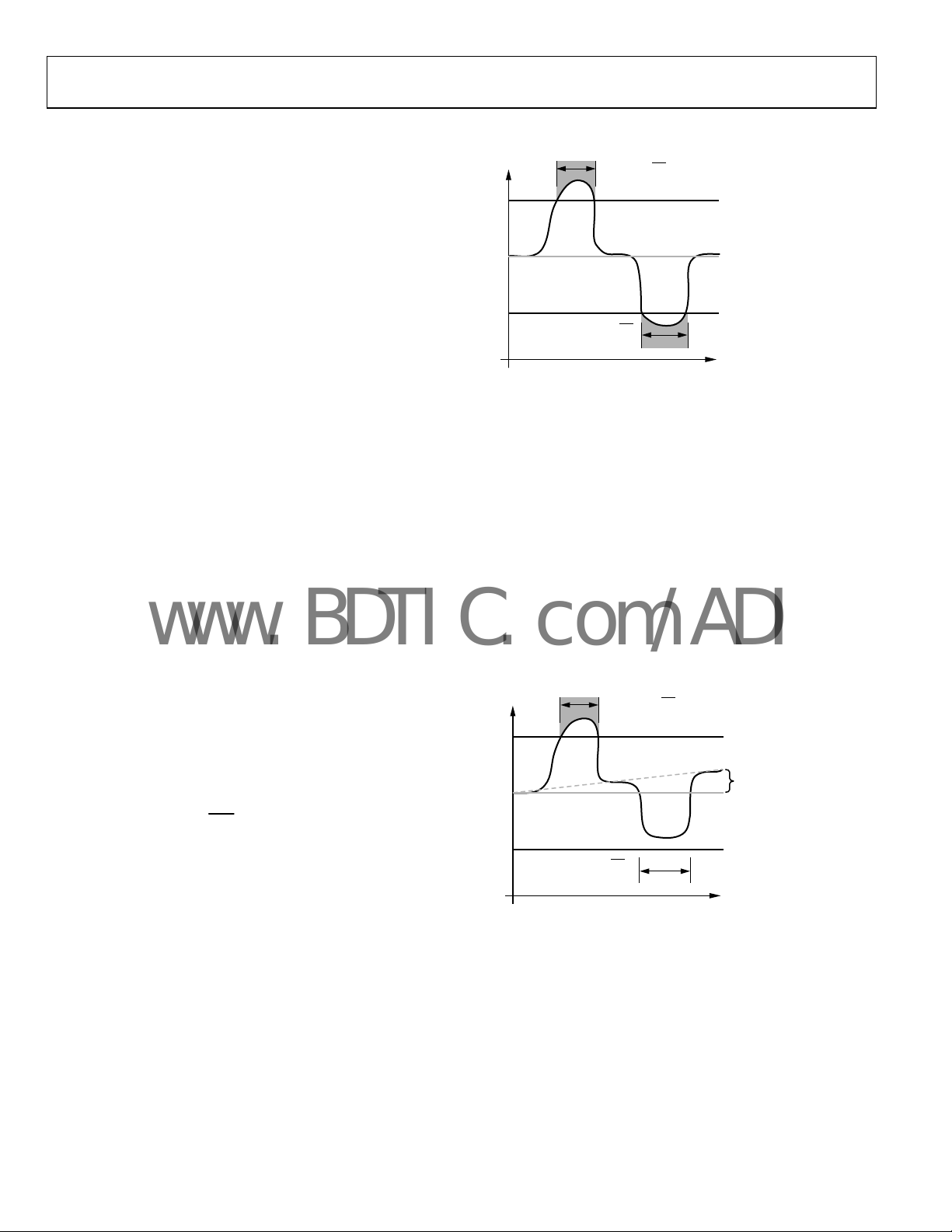
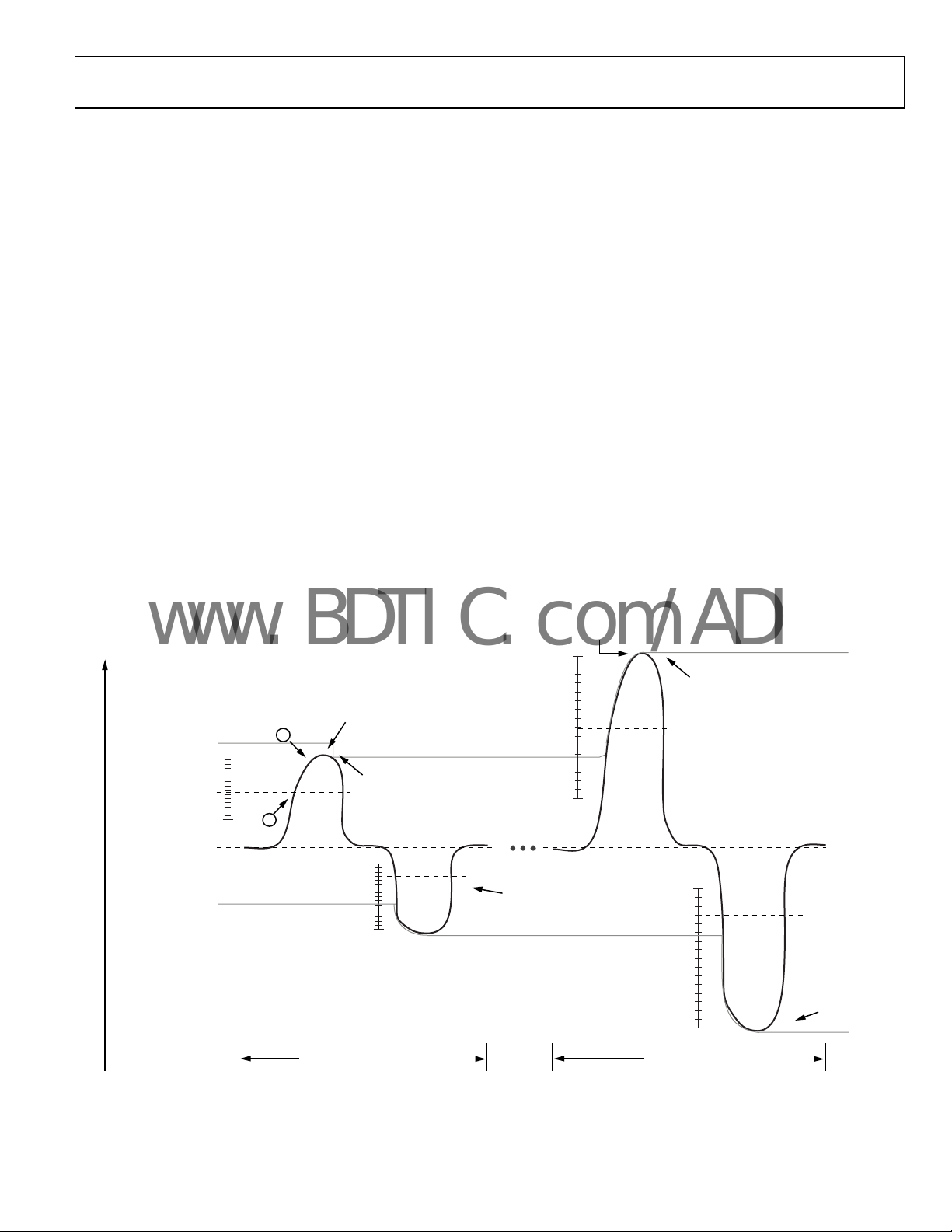
ENVIRONMENTAL CALIBRATION
The AD7143 provides on-chip capacitance sensor calibration to
automatically adjust for environmental conditions that have an
effect on the capacitance sensor ambient levels. Capacitance
sensor output levels are sensitive to temperature, humidity, and
in some cases, dirt. The AD7143 achieves optimal and reliable
sensor performance by continuously monitoring the CDC
ambient levels and correcting for any changes by adjusting the
STAGE_HIGH_THRESHOLD and STAGE_LOW_THRESHOLD
register values as described in Equation 1 and Equation 2. The
CDC ambient level is defined as the capacitance sensor output
level during periods when the user is not approaching or in
contact with the sensor.
The compensation logic runs automatically on every conversion
a
fter configuration when the AD7143 is not being touched. This
allows the AD7143 to account for rapidly changing
environmental conditions.
The ambient compensation control registers located at
A
ddress 0x002, Address 0x003 and Address 0x004 give the host
access to general setup and controls for the compensation
algorithm. The RAM stores the compensation data for each
conversion stage, as well as setup information specific to each stage.
Figure 33 sh
ows an example of an ideal capacitance sensor
behavior where the CDC ambient level remains constant
regardless of the environmental conditions. The CDC output
shown is for a pair of differential button sensors, where one
sensor caused an increase, and the other a decrease in measured
capacitance when activated.
The positive and negative sensor threshold levels are calculated
as a p
ercentage of the STAGE_OFFSET_HIGH and
STAGE_OFFSET_LOW values based on the threshold
sensitivity settings and the ambient value. These values for this
example are sufficient to detect a sensor contact, resulting with
the AD7143 asserting the
INT
output when the threshold levels
are exceeded.
CDC OUTPUT CODES
CHANGING ENVI RONMENTAL CO NDITIO NS
Figure 33. Ideal Sensor Behavior with a Constant Ambient Level
CAPACITANCE SENSOR BEHAVIOR WITHOUT CALIBRATION
Figure 34 shows the typical behavior of a capacitance sensor
with no applied calibration. This figure shows ambient levels
drifting over time as environmental conditions change. The
ambient level drift has resulted in the detection of a missed user
contact on Sensor 2.
This is a result of the initial STAGE_LOW_THRESHOLD
emaining constant while the ambient levels drifted upward
r
beyond the detection range. The Capacitance Sensor Behavior
with Calibration section describes how the AD7143 adaptive
calibration algorithm prevents errors such as this from
occurring.
CDC OUTPUT CODES
NOT ASSERTED
CHANGING ENVIRONMENTAL CO NDITIONS
Figure 34. Typical Sensor Behavior without Calibration Applied
SENSOR 1 INT
ASSERTED
SENSOR 2 INT
ASSERTED
SENSOR 1 INT
SENSOR 2 INT
ASSERTED
STAGE_HIG H_THRESHOLD
CDC AMBIENT VALUE
STAGE_LOW_THRESHOLD
t
STAGE_HIG H_THRESHOL D
CCDC AMBIENT
VALUE DRIFTING
STAGE_LOW_THRESHOLD
t
06472-030
06472-031
Rev. 0 | Page 22 of 56
AD7143
www.BDTIC.com/ADI
CAPACITANCE SENSOR BEHAVIOR WITH CALIBRATION
The AD7143 on-chip adaptive calibration algorithm prevents
sensor detection errors, such as the one shown in Figure 34.
This is achi
readjusting the initial STAGE_OFFSET_HIGH and
STAGE_OFFSET_LOW values according to the amount of
ambient drift measured on each sensor.
The internal STAGE_HIGH_THRESHOLD and
AGE_LOW_THRESHOLD values, shown in Equation 1 and
ST
Equation 2, are automatically updated based on the new
STAGE_OFFSET_HIGH and STAGE_OFFSET_LOW values.
This closed-loop routine ensures the reliability and repeatable
operation of every sensor connected to the AD7143 under
dynamic environmental conditions. Figure 35 shows a
simplified example of how the AD7143 applies the adaptive
calibration process resulting in no interrupt errors under
changing CDC ambient levels due to environmental conditions.
On-Chip Logic Stage High Threshold Calculation
eved by monitoring the CDC ambient levels and
⎛
⎛
⎜
⎜
⎝
⎜
⎜
⎜
⎝
HIGHOFFSETSTAGE
__
−
16
____
4
1
CDC OUTPUT CODES
4
CHANGING ENVIRO NMENTAL CO NDITIONS
1
INITIAL STAGE_OFFSET_HIGH REGISTER VALUE.
2
POST CALI BRATED REGI STER STAGE_HIGH_THRESHOLD.
3
POST CALI BRATED REGI STER STAGE_HIGH_THRESHOLD.
4
INITIAL STAGE_LO W_THRESHOLD.
5
POST CALI BRATED REGISTER STAGE_L OW_THRESHOLD.
6
POST CALI BRATED REGISTER STAGE_L OW_THRESHOLD.
Figure 35. Typical Sensor Behavior with Calibration Applied on the Data Path
AMBIENTSFSTAGETHRESHOLDHIGHSTAGE
⎛
⎜
⎝
HIGHOFFSETSTAGE
__
⎞
⎞
⎟
⎟
⎠
⎟
×
⎟
⎟
⎠
4
SENSOR 1 INT
ASSERTED
2
5
SENSOR 2 INT
ASSERTED
HIGHOFFSETSTAGE
__
⎞
++=
⎟
⎠
__
3
6
(1)
YSENSITIVITTHRESHOLDPOS
STAGE_HIG H_THRESHOLD
(POST CALI BRATED
REGISTER VALUE)
CDC AMBIENT
VALUE DRIFTING
STAGE_LOW_THRESHOLD
(POST CALI BRATED
REGISTER VALUE)
t
06472-032
On-Chip Logic Stage Low Threshold Calculation
⎛
⎛
⎜
⎜
⎝
⎜
⎜
⎜
⎝
LOWOFFSETSTAGE
__
−
16
LOWOFFSETSTAGE
__
AMBIENTSFSTAGETHRESHOLDLOWSTAGE
____
4
⎛
⎜
⎝
LOWOFFSETSTAGE
__
⎞
⎞
⎟
⎟
⎠
⎟
×
⎟
⎟
⎠
4
⎞
++=
⎟
⎠
(2)
__
YSENSITIVITTHRESHOLDNEG
Rev. 0 | Page 23 of 56
AD7143
www.BDTIC.com/ADI
Table 12. Additional Information about Environmental Calibration and Adaptive Threshold Registers
Register Location Description
NEG_THRESHOLD_SENSITIVITY Bank 2 Used in Equation 2. This value is programmed once at start up.
NEG_PEAK_DETECT Bank 2
POS_THRESHOLD_SENSITIVITY Bank 2 Used in Equation 1. This value is programmed once at startup.
POS_PEAK_DETECT Bank 2
STAGE_OFFSET_LOW Bank 2
STAGE_OFFSET_HIGH Bank 2
STAGE_OFFSET_HIGH_CLAMP Bank 2 Used by Internal Environmental Calibration and Adaptive Threshold Algorithms Only.
STAGE_OFFSET_LOW_CLAMP Bank 2 Used by Internal Environmental Calibration and Adaptive Threshold Algorithms Only.
STAGE_SF_AMBIENT Bank 3
STAGE_HIGH_THRESHOLD Bank 3 Equation 1 Value.
STAGE_LOW_THRESHOLD Bank 3 Equation 2 Value.
Used by Internal Adaptive Threshold Logic Only
percentage of the difference between the ambient CDC value and the minimum
average CDC value. If the output of the CDC gets within the NEG_PEAK_DETECT
percentage of the minimum average, only then is the minimum average value updated.
Used by Internal Adaptive Threshold Logic Only. The POS_PEAK_DETECT is set to a
centage of the difference between the ambient CDC value, and the maximum
per
average CDC value. If the output of the CDC gets within the POS_PEAK_DETECT
percentage of the minimum average, only then is the maximum average value updated.
Used in Equation 2. An initial value (based on se
into this register at startup. The AD7143 on-chip calibration algorithm automatically
updates this register based on the amount of sensor drift due to changing ambient
conditions. Set to 80% of the STAGE_OFFSET_LOW_CLAMP value.
Used in Equation 1. An initial value (based on se
into this register at startup. The AD7143 on-chip calibration algorithm automatically
updates this register based on the amount of sensor drift due to changing ambient
conditions. Set to 80% of the STAGE_OFFSET_HIGH_CLAMP value.
An initial value (based on sensor characterization) is programmed into this register at
startup. The value in this register prevents a user from causing a sensor output value to
exceed the expected nominal value. Set to the maximum expected sensor response,
maximum change in CDC output code.
An initial value (based on sensor characterization) is programmed into this register at
startup. The value in this register prevents a user from causing a sensor output value to
exceed the expected nominal value. Set to the minimum expected sensor response,
minimum change in CDC output code .
Used in Equation 1 and Equation 2. This is the ambien
is not touched, as calculated using the slow FIFO.
. The NEG_PEAK_DETECT is set to a
nsor characterization) is programmed
nsor characterization) is programmed
t sensor output, when the sensor
Rev. 0 | Page 24 of 56
AD7143
A
W
www.BDTIC.com/ADI
ADAPTIVE THRESHOLD AND SENSITIVITY
The AD7143 provides an on-chip self-learning adaptive
threshold and sensitivity algorithm. This algorithm continuously monitors the output levels of each sensor and automatically
rescales the threshold levels proportionally to the sensor area
covered by the user. As a result, the AD7143 maintains optimal
threshold and sensitivity levels for all types of users regardless
of their finger sizes.
The threshold level is always referenced from the ambient level
nd is defined as the CDC converter output level that must be
a
exceeded for a valid sensor contact. The sensitivity level is
defined as how sensitive the sensor is before a valid contact is
registered.
Figure 36 p
rovides an example of how the adaptive threshold and
sensitivity algorithm works. The positive and negative sensor
threshold levels are calculated as a percentage of the
STAGE_OFFSET_HIGH and STAGE_OFFSET_LOW values
based on the threshold sensitivity settings and the ambient value.
On configuration, initial estimates are supplied for both
AGE_OFFSET_HIGH and STAGE_OFFSET_LOW after
ST
which the calibration engine automatically adjusts the
STAGE_HIGH_THRESHOLD and STAGE_LOW_THRESHOLD
values for sensor response.
Reference A in Fi
gure 36 shows an under sensitive threshold
level for a small finger user, demonstrating the disadvantages of
a fixed threshold level. By enabling the adaptive threshold and
sensitivity algorithm, the positive and negative threshold levels
are determined by the POS_THRESHOLD_SENSITIVITY and
NEG_THRESHOLD_SENSITIVITY register values and the
most recent average maximum sensor output value. These
registers can be used to select 16 different positive and negative
sensitivity levels ranging between 25% and 95.32% of the most
recent average maximum output level referenced from the
ambient value. The smaller the sensitivity percentage setting,
the easier it is to trigger a sensor activation. Reference B shows
that the positive adaptive threshold level is set at almost midsensitivity with a 62.51% threshold level by setting
POS_THRESHOLD_SENSITIVITY = 1000. Figure 36 also
provides a similar example for the negative threshold level with
NEG_THRESHOLD_SENSITIVITY = 0001.
STAGE_OFFSET_HIGH
CDC OUTPUT CODE S
THRESHOLD LEVEL
AMBIENT LEVEL
STAGE_OFFSET_LOW
AVERAGE MAX VAL UE
A
95.32%
62.51% = POS
ADAPTIVE
B
25%
NEG ADAPTIVE THRESHOLD LEVEL = 39.08%
SENSOR CONTACTED
BY SMALL FINGER
Figure 36. Threshold Sensitivity Example with POS_THRESHOLD_SENSITIVIT
STAGE_OFFSET_HIGH
IS UPDATED HERE
25%
95.32%
62.51% = POS ADAPT IVE
THRESHOLD LEVEL
VERAGE MAX VALUE
95.32%
25%
STAGE_OFFSET_LOW
IS UPDATED HERE
NEG ADAPTIV E THRESHOL D LEVEL = 39.08%
Y = 1000 and NEG_THRESHOLD_SENSITIVITY = 0011
25%
95.32%
SENSOR CONTACTED
BY LARGE FI NGER
STAGE_OFFSET _HIGH
IS UPDATED
STAGE_OFFSET _LO
IS UPDATED HERE
6472-033
Rev. 0 | Page 25 of 56

AD7143
www.BDTIC.com/ADI
INTERRUPT OUTPUT
The AD7143 has an interrupt output that triggers an interrupt
INT
service routine on the host processor. The
signal is on
Pin 14, and is an open-drain output. There are two types of
interrupt events on the AD7143: a CDC conversion complete
interrupt and a sensor touch interrupt. Each interrupt has
enable and status registers described in Ta b l e 13 . The
conversion complete and sensor threshold interrupts can be
enabled on a per conversion stage basis. The status registers
indicate what type of interrupt triggered the
registers are cleared, and the
INT
signal is reset high, during a
INT
pin. Status
read operation of the interrupt status registers. The signal
returns high as soon as the read address has been set up.
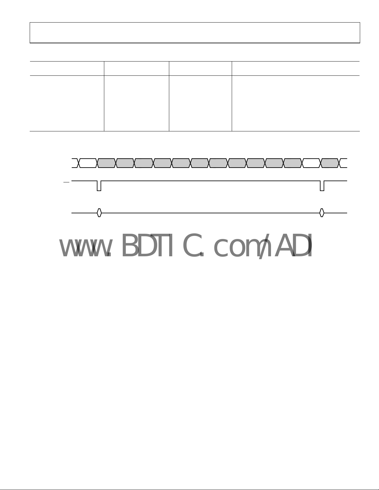
CDC CONVERSION COMPLETE INTERRUPT
The AD7143 interrupt signal asserts low to indicate the
completion of a conversion stage, and new conversion result
data is available in the registers.
The interrupt can be independently enabled for each conversion
tage. Each conversion stage complete interrupt can be enabled
s
via the STAGE_COMPLETE_EN register (Address 0x007). This
register has a bit that corresponds to each conversion stage.
Setting this bit to 1 enables the interrupt for that stage. Clearing
this bit to 0 disables the conversion complete interrupt for that
stage.
Figure 38 shows an end of conversion interrupt timing
wi
th the STAGE0 interrupt enabled.
In normal operation, the AD7143’s interrupt is enabled only for
he last stage in a conversion sequence as shown in Figure 38.
t
Configuring the AD7143 into this mode results in the interrupt
eing asserted when the user makes contact with the sensor and
b
again when the user lifts off the sensor. The second interrupt is
required to alert the host processor that the user is no longer
contacting the sensor.
The registers located at Address 0x005 and Address 0x006 are
sed to enable the interrupt output for each stage. The registers
u
located at Address 0x008 and Address 0x009 are used to read
back the interrupt status for each stage.
Figure 37 sh
ows the interrupt output timing during contact with
one of the sensors connected to STAGE0 while operating in the
sensor touch interrupt mode. For a low limit configuration, the
interrupt output is asserted as soon as the sensor is contacted and
again after the user has stopped contacting the sensor.
Note that the interrupt output remains low until the host
rocessor reads back the interrupt status registers located at
p
Address 0x008 and Address 0x009.
The interrupt output is asserted when there is a change in the
hreshold status bits. This could indicate that a user is now
t
touching the sensor(s) for the first time, the number of sensors
being touched has changed, or the user is no longer touching
the sensor(s). Reading the status bits in the interrupt status
register shows the current sensor activations.
FINGER ON SENSOR
FINGER OFF SENSOR
31
Register 0x00A is the conversion complete interrupt status
r
egister. Each bit in this register corresponds to a conversion
stage. If a bit is set, it means that the conversion complete
interrupt for the corresponding stage was triggered. This
register is cleared on a read, provided the underlying condition
that triggered the interrupt has gone away.
SENSOR TOUCH INTERRUPT
The sensor touch interrupt mode is implemented when the host
processor requires an interrupt only when a sensor is contacted.
Rev. 0 | Page 26 of 56
CONVERSION
STAGE
SERIAL
READ BACK
INT OUTPUT
1
USER TOUCHING DOWN ON SENSOR.
2
ADDRESS 0x008 READ BACK TO CL EAR INTERRUPT .
3
USER LIFTING OFF OF SENSOR.
4
ADDRESS 0x008 READ BACK TO CL EAR INTERRUPT .
Figure 37. Example of Sensor Touch Interrupt
STAGE1STAGE0
42
06472-034
AD7143
C
www.BDTIC.com/ADI
Table 13. Interrupt Mode Registers
Interrupt Enable
Interrupt Mode
Regist
er Address
Sensor Touch
Low 0x005 0x008
High 0x006 0x009
CDC Conversion Complete 0x007 0x00A
Interrupt Status
Register Address Notes
Interrupt asserted when the user contacts a sensor.
ee Figure 37.
S
Enable for the CIN inputs connected to the CDC
positi
Enable for the CIN inputs connected to the CDC
egative stage.
n
Continuous interrupt at the end
is enabled.
ve stage.
of each STAGEx that
ONVERSIONS
INT
SERIAL
READS
STAGE0 STAGE1 STAGE2 STAGE3 STAGE4 STAGE5 STAGE6 STAGE7 STAGE8 STAGE9 STAGE10 STAGE11 STAGE0 STAGE1
NOTES
1. THIS I S AN EXAMPLE OF A CDC CONVERSI ON COMPL ETE INT ERRUPT.
2. THIS T IMING EXAMPLE SHOW S THAT THE INTERRUPT OUTPUT HAS BEE N ENABLED TO BE ASSERTED
AT THE END OF A CONVERSIO N CYCLE FOR STAGE0 ONL Y.
3. STAGEx CO NFIGURAT ION PROG RAMMING NOTES FOR S TAGE0, ST AGE5, AND ST AGE9 (x = 0, 5, 9)
STAGEx_L OW_INT _EN (ADDRESS 0x005) = 0
STAGEx_HI GH_INT_EN (ADDRESS 0x006) = 0
STAGEx_CO MPLETE_EN (ADDRESS 0x007) = 1
Figure 38. Example of Configuring the Registers for
End of Conversion Interrupt Setup
21
06472-035
Rev. 0 | Page 27 of 56

AD7143
www.BDTIC.com/ADI
SERIAL INTERFACE
The AD7143 is available with a fixed address I2C-compatible
interface.
I2C COMPATIBLE INTERFACE
The AD7143 supports the industry standard 2-wire I2C serial
interface protocol. The two wires associated with the I
the SCLK and the SDA inputs. The SDA is an I/O pin that allows
both register write and register readback operations. The AD7143 is
always a slave device on the I
2
C serial interface bus.
The AD7143 has a single fixed 7-bit device address,
ddress 0101 110. The AD7143 responds when the master
A
device sends its device address over the bus. The AD7143
cannot initiate data transfers on the bus.
Table 14. AD7143 I
DEV
A6
DEV
A5
2
C Fixed Device Address
DEV
A4
DEV
A3
DEV
A2
0 1 0 1 1 1 0
Data Transfer
Data is transferred over the I2C serial interface in 8-bit bytes.
The master initiates a data transfer by establishing a start condition, defined as a high-to-low transition on the serial data
line, SDA, while the serial clock line, SCLK, remains high. This
indicates that an address/data stream follows.
2
C timing are
DEV
A1
DEV
A0
All slave peripherals connected to the serial bus respond to the
art condition and shift in the next eight bits, consisting of a
st
7-bit address (MSB first) plus an R/
W
bit that determines the
direction of the data transfer. The peripheral whose address
corresponds to the transmitted address responds by pulling the
data line low during the ninth clock pulse. This is known as the
acknowledge bit. All other devices on the bus now remain idle
while the selected device waits for data to be read from, or
written to it. If the R/
device. If the R/
W
bit is a 0, the master writes to the slave
W
bit is a 1, the master reads from the slave device.
Data is sent over the serial bus in a sequence of nine clock
ulses, eight bits of data followed by an acknowledge bit from
p
the slave device. Transitions on the data line must occur during
the low period of the clock signal and remain stable during the
high period, since a low-to-high transition when the clock is
high can be interpreted as a stop signal. The number of data
bytes transmitted over the serial bus in a single read or write
operation is limited only by what the master and slave devices
can handle.
When all data bytes are read or written, a stop condition is
stablished. A stop condition is defined by a low-to-high
e
transition on SDA while SCLK remains high. If the AD7143
encounters a stop condition, it returns to its idle condition, and
the address pointer register resets to Address 0x00.
START
SDA
t
SCLK
NOTES
1. A START CONDITION AT THE BEGINNING IS DEF INED AS A HIGH- TO-LO W TRANSIT ION ON SDA W HILE SCLK REMAINS HIGH.
2. A STOP CO NDITION AT THE END IS DEFINED AS A LOW-TO -HIGH TRANSI TION O N SDA WHILE SCLK REMAINS HIGH.
3. 7-BIT DEVICE ADDRESS [DEV A6:DEV A0] = [ 0 1 0 1 1 1 0].
4. 16-BIT REG ISTER ADDRESS [A15:A0] = [X, X, X, X, X, X, A9, A8, A7, A6, A5, A4, A3, A2, A1, A0], W HERE X ARE DON’T CARE BITS.
5. REGIST ER ADDRESS [A15:A8] AND REGISTER ADDRESS [A7:A0] ARE ALW AYS SEPARATE D BY A LOW ACK BI T.
6. REGIST ER DATA [D15:D8] AND REG ISTER DAT A [D7:D0] ARE ALWAYS SEPARATED BY A LOW ACK BIT .
1
D15 D14
ACK ACK
AD7143 DEVICE ADDRESS
DEVA6DEVA5DEV
126234
REGISTER DATA [D15:D8] REGISTER DAT A [D7:D0]
A4
DEVA2DEVA1DEV
DEV
A3
5678910
t
2
D9 D8
t
4
3527 28 29 34 3736 4338 44
Figure 39. Example of I
R/W
A0
t
3
t
REGISTER ADDRESS [A15:A8] REGISTE R ADDRESS [A7:A0]
ACK A15 A14
5
2
C Timing for Single Register Write Operation
A9 A8
11
D1 D0D7 D6
ACK
45 46
ACK
17 18 19 20 25
16
STOP
t
8
t
6
A7 A6
START
t
7
A1 A0
AD7143 DEVICE ADDRESS
DEVA6DEVA5DEV
123
A4
6472-036
Rev. 0 | Page 28 of 56

AD7143
www.BDTIC.com/ADI
Writing Data over the I2C Bus
The process for writing to the AD7143 over the I2C bus is
shown in Figure 39 and Figure 41. The device address is sent
W
over the bus followed by the R/
by two bytes of data that contain the 10-bit address of the
internal data register to be written. The following bit map shows
the upper register address bytes. Note that Bit 7 to Bit 2 in the
upper address byte are don’t care bits. The address is contained
in the 10 LSBs of the register address bytes.
MSB LSB
7 6 5 4 3 2 1 0
X X X X X X
The following bit map shows the lower register address bytes.
MSB LSB
7 6 5 4 3 2 1 0
Reg.
Addr.
Bit 7 Bit 6 Bit 5 Bit 4 Bit 3 Bit 2 Bit 1 Bit 0
The third data byte contains the 8 MSBs of the data to be
written to the internal register. The fourth data byte contains
the 8 LSBs of data to be written to the internal register.
Reg.
Addr.
Reg.
Addr.
Reg.
Addr.
bit set to 0. This is followed
Reg.
Addr.
Register
A
Bit 9
Reg.
Addr.
ddress
Reg.
Addr.
Register
Address
Bit 8
Reg.
Addr.
Any data written to the AD7143 after the address pointer has
eached its maximum value is discarded.
r
All registers on the AD7143 are 16-bit. Two consecutive 8-bit
ata bytes are combined and written to the 16-bit registers. To
d
avoid errors, all writes to the device must contain an even
number of data bytes.
To finish the transaction, the master generates a stop condition
o
n SDA, or generates a repeat start condition if the master is to
maintain control of the bus.
Reading Data over the I2C Bus
To read from the AD7143, the address pointer register must first
be set to the address of the required internal register. The master
performs a write transaction, and writes to the AD7143 to set the
address pointer. The master then outputs a repeat start condition
to keep control of the bus, or, if this is not possible, ends the write
transaction with a stop condition. A read transaction is initiated,
with the R/
The AD7143 supplies the upper eight bits of data from the
addr
lower eight bits in the next byte. This is shown in Figure 40 and
Figure 41.
W
bit set to 1.
essed register in the first readback byte, followed by the
The AD7143 address pointer register automatically increments
fter each write. This allows the master to sequentially write to all
a
registers on the AD7143 in the same write transaction. However,
the address pointer register does not wrap around after the last
address.
Because the address pointer automatically increases after each
r
ead, the AD7143 continues to output readback data until the
master puts a no acknowledge and stop condition on the bus. If
the address pointer reaches its maximum value, and the master
continues to read from the part, the AD7143 repeatedly sends
data from the last register addressed.
Rev. 0 | Page 29 of 56

AD7143
W
www.BDTIC.com/ADI
SEPARATE READ AND
START
SDA
SCLK
REPEATED START
RITE TRANSACTI ONS
USING
NOTES
1. A START CONDI TION AT T HE BEGINNING IS DEFINED AS A HI GH-TO-L OW TRANSI TION ON SDA W HILE SCLK REM AINS HIGH.
2. A STOP CONDI TION AT T HE END IS DEFI NED AS A LOW-T O-HIGH T RANSITIO N ON SDA WHILE S CLK REMAINS HIG H.
3. THE MASTER G ENERATES THE ACK AT THE END OF T HE READBACK TO SIG NAL THAT IT DOES NOT W ANT ADDITIO NAL DATA.
4. 7-BIT DEVICE ADDRESS [DEV A6:DEV A0] = [0 1 0 1 1 1 0].
5. 16-BIT REGISTER ADDRESS[A15:A0] = [X, X, X, X, X, X, A9, A8, A7, A6, A5, A4, A3, A2, A1, A0], WHERE THE UPPER LSB Xs ARE DON’T CARE BITS.
6. REGISTE R ADDRESS [A15:A8] AND REGISTER ADDRESS [A7:A0] ARE ALWAYS SEPARATED BY LOW ACK BITS.
7. REGISTE R DATA [D15:D8] AND REGIST ER DATA [D7:D0] ARE ALWAY S SEPARATED BY A LOW ACK BIT.
8. THE R/W BI T IS SET T O A1 TO I NDICATE A READBACK OPERAT ION.
AD7143 DEVICE ADDRESS
DEVA6DEVA5DEV
t
1
A4
1 26234 17 18 19 20 25
SR
28 30
P
DEVA2DEVA1DEV
DEV
A3
t
2
AD7143 DEVICE ADDRESS
DEVA6DEV
A5
29
S
DEVA6DEV
29
28
Figure 40. Example of I
WRITE
7-BIT DEVICE
S
ADDRESS
READ (USING REPEATED START)
7-BIT DEVICE
S
ADDRESS
READ (WRITE T RANSACTION SE TS UP REGIS TER ADDRESS)
7-BIT DEVICE
S
ADDRESS
OUTPUT FROM MASTER
OUTPUT FROM AD7143
REGISTER ADDR
W
ACK
REGISTER ADDR
W
ACK
REGISTER ADDR
W
ACK
[15:8]
HIGH BY TE
HIGH BY TE
S = START BIT
P = STOP BIT
SR = REPEATED START BIT
REGISTER ADDR
[7:0]
ACK
REGISTER ADDR
LOW BYTE
ACK
REGISTER ADDR
LOW BYTE
ACK
Figure 41. Example of Sequential I
R/W
A0
t
3
AD7143 DEVICE ADDRESS
A5
30
ACK A15 A14
DEVA1DEV
A0
t
4
35
34 3736 4 438 45
DEVA1DEV
34 3736 4438 45
WRITE DATA
HIGH BYTE [15:8]
ACK
6-BIT DEVICE
SR
ADDRESS
ACK
6-BIT DEVICE
P
S
ACK
ADDRESS
ACK = ACKNOWLEDG E BIT
ACK = NO ACKNOWLE DGE BIT
REGISTER ADDRESS [A15:A8] REGISTER ADDRESS [A7:A0]
A9 A8
11 165678910
REGISTER DAT A [D7:D0]
ACK
R/W
t
5
39
REGISTER DATA [D7:D0]
ACK
R/W
A0
t
4
35
2
C Timing for Single Register Readback Operation
WRITE DATA
LOW BYTE [7:0]
ACK
READ DATA
R
HIGH BYTE [15:8]
ACK
READ DATA
R
HIGH BYT E [15:8]
ACK
2
C Write and Readback Operation
t
5
39
WRITE DATA
HIGH BYT E [15:8]
READ DATA
LOW BYTE [7:0]
ACK
ACK
A7 A6
ACK
D1 D0D7 D6
D1 D0D7 D6
READ DATA
LOW BYTE [7:0]
ACK
t
46
ACK
WRITE DATA
LOW BYTE [7:0]
ACK
READ DATA
HIGH BYTE [15:8]
P
6
46
HIGH BYT E [15:8]
t
8
P
READ DATA
A1 A0
P
ACK
ACK
ACK
AD7143 DEVICE ADDRESS
DEVA6DEVA5DEV
t
7
READ DATA
LOW BYTE [7:0]
READ DATA
LOW BYTE [7:0]
ACK
27
A4
123
P
ACK
ACK
06472-037
P
6472-038
Rev. 0 | Page 30 of 56

AD7143
www.BDTIC.com/ADI
PCB DESIGN GUIDELINES
CAPACITIVE SENSOR BOARD MECHANICAL SPECIFICATIONS
Table 15.
Parameter Symbol Min Typ Max Unit
Distance from Edge of Any Sensor to Edge of Metal Object D
Distance Between Sensor Edges
1
Distance Between Bottom of Sensor Board and Controller Board or Metal Casing2 (4-Layer,
2-Layer, and Flex Circuit)
1
The distance is dependent on the application and the positioning of the switches relative to each other and with respect to the user’s finger positioning and handling.
Adjacent sensors, with 0 minimum space between them, are implemented differentially.
2
The 1.0 mm specification is meant to prevent direct sensor board contact with any conductive material. This specification does not guarantee no EMI coupling from
the controller board to the sensors. Address potential EMI coupling issues by placing a grounded metal shield between the capacitive sensor board and the main
controller board as shown in Figure 44.
1
D2 = D3 = D40 mm
D
5
1.0 mm
1.0 mm
METAL OBJECT
CAPACITIVE SENSOR
PRINTED CIRCUIT
SLIDER
BUTTONS
D
2
D
1
Figure 42. Capacitive Sensor Board Mechanicals Top View
CAPACITIVE SE NSOR BOARD
D
5
CONTROLL ER PRINTED CIRCUIT BOARD OR METAL CASING
Figure 43. Capacitive Sensor Board Mechanicals Side View
GROUNDED METAL SHIELD
8-WAY
SWITCH
D
4
D
3
D
5
CONTROLL ER PRINTED CIRCUIT BOARD OR METAL CASING
Figure 44. Capacitive Sensor Board with Grounded Shield
CAPACITIVE S ENSOR BOARD
06472-041
CHIP SCALE PACKAGES
The lands on the chip scale package (CP-16-13) are rectangular.
The printed circuit board pad for these should be 0.1 mm
longer than the package land length, and 0.05 mm wider than
the package land width. Center the land on the pad to maximize
the solder joint size.
The bottom of the chip scale package has a central thermal pad.
hermal pad on the printed circuit board should be at least
The t
as large as this exposed pad. To avoid shorting, provide a
clearance of at least 0.25 mm between the thermal pad and the
inner edges of the land pattern on the printed circuit board.
06472-039
06472-040
Thermal vias can be used on the printed circuit board thermal
ad to improve thermal performance of the package. If vias are
p
used, they should be incorporated in the thermal pad at a
1.2 mm pitch grid. The via diameter should be between 0.3 mm
and 0.33 mm, and the via barrel should be plated with 1 oz.
copper to plug the via.
Connect the printed circuit board thermal pad to GND.
Rev. 0 | Page 31 of 56
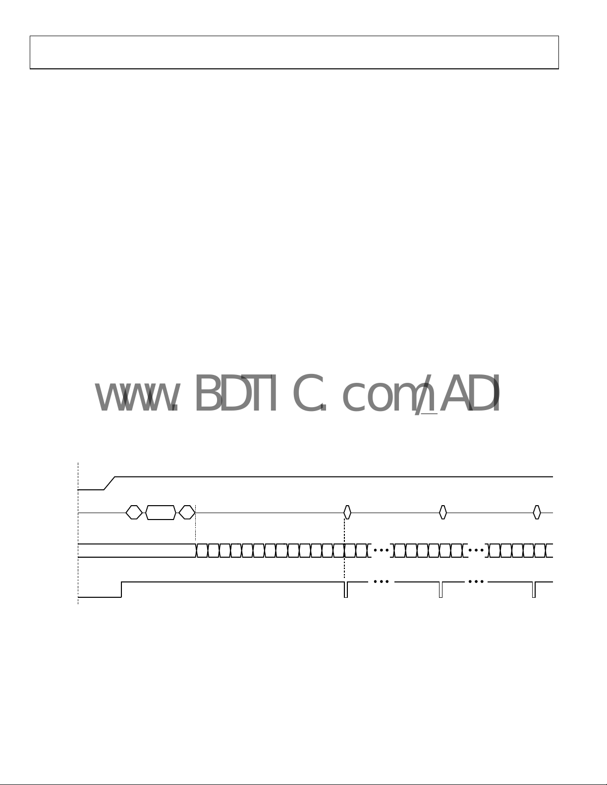
AD7143
www.BDTIC.com/ADI
POWER-UP SEQUENCE
When the AD7143 is powered up, the following sequence is
recommended when initially developing the AD7143 and
Host µC serial interface:
urn on the power supplies to the AD7143.
1. T
2. W
rite to the Bank 2 registers at Address 0x080 through
Address 0x0DF. These registers are contiguous, so a
sequential register write sequence can be applied.
Note: The Bank 2 register values are unique for each
pplication. Register values are provided by Analog
a
Devices after the sensor board has been developed.
rite to the Bank 1 registers at Address 0x000 through
3. W
Address 0x007 as outlined below. These registers are
contiguous so a sequential register write sequence can be
applied
Caution: At this time, Address 0x001 must remain set to
defa
ult value 0x0000 during this contiguous write
operation.
Register values:
Address 0x000 = 0x00B2
Address 0x001 = 0x0000
Address 0x002 = 0x0690
Address 0x003 = 0x0664
Address 0x004 = 0x290F
Address 0x005 = 0x0000
Address 0x006 = 0x0000
Address 0x007 = 0x0001 (The AD7143 interrupt is asserted
pproximately every 25 ms.)
a
4. W
rite to the Bank 1 register, Address 0x001 = 0x0FFF.
5. Re
ad back the corresponding interrupt status register at
Address 0x008, Address 0x009, or Address 0x00A. This is
determined by the interrupt output configuration as
explained in the
Interrupt Output section.
Note: The specific registers required to be readback depend
n each application. Analog Devices provides this
o
information after the sensor board has been developed.
POWER
HOST
SERIAL
INTERFACE
CONVERSIO N
STAGE
AD7143 INT
CONVERSION STAGES DISABLED
6. Rep
1 2 3 4 5 6 7 8 9 10 11 0 1 2
0
FIRST CONVERSION SEQ UENCE
Figure 45. Recommended Start-Up Sequence
eat Step 5 each time
910110 1 2 910110 1
SECOND CONVE RSION
SEQUENCE
INT
is asserted.
THIRD CONV ERSION
SEQUENCE
6472-042
Rev. 0 | Page 32 of 56
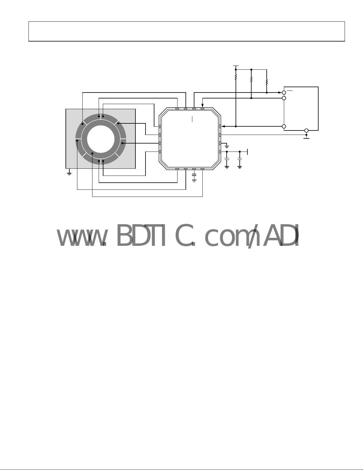
AD7143
V
www.BDTIC.com/ADI
TYPICAL APPLICATION CIRCUITS
DRIVE
2.2kΩ
2.2kΩ
2.2kΩ
INT
SCLK
HOST WITH
2
C
I
13
14
15
16
INT
CIN0
CIN1
1CIN2
SCROLL
WHEEL
SENSORS TO GROUND
FLOODED PLANE AROUND
RECOMMENDED TO CONNECT
SENSOR PCB
2CIN3
3CIN4
4CIN5
AD7143
5 CIN6
Figure 46. Typical Application Circuit with I
6 CIN7
10nF
SCLK
12SDA
11VDRIVE
10GND
9VCC
7 CSHIELD
8 SRC
0.1µF
2
C Interface
VCC
2.7V TO 3.6V
1µF TO 10µF
(OPTIONAL)
INTERFACE
V
SDA
OPTIONAL
2
C INTERFACE
I
VOLTAGE
(1.65V TO 3.6V)
HOST
6472-043
Rev. 0 | Page 33 of 56
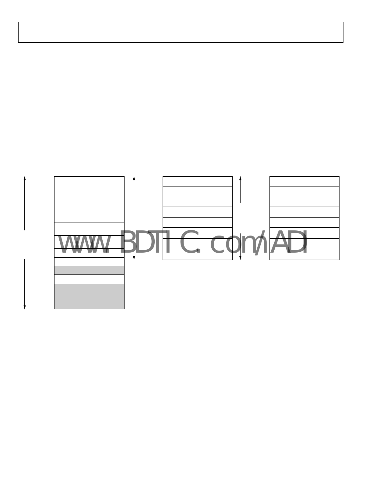
AD7143
www.BDTIC.com/ADI
REGISTER MAP
The AD7143 address space is divided into three different
register banks, referred to as Bank 1, Bank 2, and Bank 3.
Figure 47 illustrates the division of these three banks.
Bank 1 registers contain control registers, CDC conversion
ontrol registers, interrupt enable registers, interrupt status
c
registers, CDC 16-bit conversion data registers, device ID
registers, and proximity status registers.
Bank 2 registers contain the configuration registers used for
uniq
uely configuring the CIN inputs for each conversion stage.
Initialize the Bank 2 configuration registers immediately after
power-up to obtain valid CDC conversion result data.
ADDR 0x000
ADDR 0x001
ADDR 0x005
ADDR 0x008
ADDR 0x00B
ADDR 0x013
24 REGISTERS
ADDR 0x017
ADDR 0x018
ADDR 0x042
ADDR 0x043
REGIST ER BANK 1
SET UP CONT ROL
(1 REGISTER)
CALIBRATI ON AND SET UP
(4 REGISTERS)
INTERRUPT ENABLE
(3 REGISTERS)
INTERRUPT STATUS
(3 REGISTERS)
CDC 16-BIT CONVERSION DAT A
(8 REGISTERS)
UNUSED (4 REGISTERS)
DEVICE ID REGISTER
INVALID DO NOT ACCES S
PROXIMITY STATUS REGISTER
ADDR 0x080
ADDR 0x088
ADDR 0x090
ADDR 0x098
ADDR 0x0A0
ADDR 0x0A8
64 REGISTE RS
ADDR 0x0B0
ADDR 0x0B8
Bank 3 registers contains the results of each conversion stage.
T
hese registers automatically update at the end of each conversion
sequence. Although these registers are primarily used by the
AD7143 internal data processing, they are accessible by the host
processor for additional external data processing, if desired.
Default values are undefined for Bank 2 registers and Bank 3
gisters until after power up and configuration of the Bank 2
re
registers.
REGIST ER BANK 2
STAGE0 CO NFIGURAT ION
(8 REGISTERS)
STAGE1 CO NFIGURAT ION
(8 REGISTERS)
STAGE2 CO NFIGURAT ION
(8 REGISTERS)
STAGE3 CO NFIGURAT ION
(8 REGISTERS)
STAGE4 CO NFIGURAT ION
(8 REGISTERS)
STAGE5 CO NFIGURAT ION
(8 REGISTERS)
STAGE6 CO NFIGURAT ION
(8 REGISTERS)
STAGE7 CO NFIGURAT ION
(8 REGISTERS)
ADDR 0x0E0
ADDR 0x088
ADDR 0x090
ADDR 0x098
ADDR 0x0A0
ADDR 0x0A8
288 REGISTERS
ADDR 0x0B0
ADDR 0x0B8
REGISTER BANK 3
STAGE0 RESULTS
(36 REGISTERS)
STAGE1 RESULTS
(36 REGISTERS)
STAGE2 RESULTS
(36 REGISTERS)
STAGE3 RESULTS
(36 REGISTERS)
STAGE4 RESULTS
(36 REGISTERS)
STAGE5 RESULTS
(36 REGISTERS)
STAGE6 RESULTS
(36 REGISTERS)
STAGE7 RESULTS
(36 REGISTERS)
ADDR 0x7F0
INVALID DO NOT ACCES S
Figure 47. Layout of Bank 1 Registers, Bank 2 Registers, and Bank 3 Registers
Rev. 0 | Page 34 of 56
06472-044
AD7143
www.BDTIC.com/ADI
DETAILED REGISTER DESCRIPTIONS
BANK 1 REGISTERS
All addresses and default values are expressed in hexadecimal format.
Table 16. PWR_CONTROL Register
Address Data Bit Default Type Name Description
0x000
[1:0] 0 R/W POWER_MODE
[3:2] 0 LP_CONV_DELAY
[7:4] 0 SEQUENCE_STAGE_NUM
[9:8] 0 DECIMATION
[10] 0 SW_RESET
[11] 0 INT_POL
[12] 0 EXCITATION_SOURCE
[13] 0 Unused Set unused register bits = 0
[15:14] 0 CDC_BIAS
Operating modes
00 = full po
approximately every 25 ms)
01 = full shutdown mode (no CDC conversions)
10 = low power mode (automatic wake-up operation)
11 = full shutdown mode (no CDC conversions)
Low power mode conversion delay
00 = 200 ms
01 = 400 ms
10 = 600 ms
11 = 800 ms
Number of stages in sequence (N + 1)
0000 = 1 c
0001 = 2 conversion stages in sequence
……
Maximum value = 1011 = 12 conversion stages per sequence
ADC decimation factor
00 = decima
01 = decimate by 128
10 = do not use this setting
11 = do not use this setting
Software reset control (self-clearing)
1 = r
Interrupt polarity control
0 = ac
1 = active high
Excitation source control for Pin 15
0 = enable output
1 = disable output
CDC bias current control
00 = normal operation
01 = normal operation + 20%
10 = normal operation + 35%
11 = normal operation + 50%
wer mode (normal operation, CDC conversions
onversion stage in sequence
te by 256
esets all registers to default values
tive low
Rev. 0 | Page 35 of 56
AD7143
www.BDTIC.com/ADI
Table 17. STAGE_CAL_EN Register
Address Data Bit Default Type Name Description
0x001
[0] 0 R/W STAGE0_CAL_EN
[1] 0 STAGE1_CAL_EN
[2] 0 STAGE2_CAL_EN
[3] 0 STAGE3_CAL_EN
[4] 0 STAGE4_CAL_EN
[5] 0 STAGE5_CAL_EN
[6] 0 STAGE6_CAL_EN
[7] 0 STAGE7_CAL_EN
[11:8] 0 Unused Set unused register bits = 0
[13:12] 0 AVG_FP_SKIP
[15:14] 0 AVG_LP_SKIP
STAGE0 calibration enable
isable
0 = d
1 = enable
STAGE1 calibration enable
isable
0 = d
1 = enable
STAGE2 calibration enable
isable
0 = d
1 = enable
STAGE3 calibration enable
isable
0 = d
1 = enable
STAGE4 calibration enable
isable
0 = d
1 = enable
STAGE5 calibration enable
isable
0 = d
1 = enable
STAGE6 calibration enable
isable
0 = d
1 = enable
STAGE7 calibration enable
isable
0 = d
1 = enable
Full power mode skip control
ip 3 samples
00 = sk
01 = skip 7 samples
10 = skip 15 samples
11 = skip 31 samples
Low power mode skip control
00 = use all sa
01 = skip 1 sample
10 = skip 2 samples
11 = skip 3 samples
mples
Rev. 0 | Page 36 of 56
AD7143
www.BDTIC.com/ADI
Table 18. AMB_COMP_CTRL0 Register
Address Data Bit Default Type Name Description
0x002
[3:0] 0 R/W FF_SKIP_CNT
[7:4] F FP_PROXIMITY_CNT Full power mode proximity period
[11:8] F LP_PROXIMITY_CNT Low power mode proximity period
[13:12] 0 PWR_DOWN_TIMEOUT
[14] 0 FORCED_CAL
[15] 0 CONV_RESET
Fast filter skip control (N+1)
0000 = no sequ
0001 = one sequence of results is skipped for every one
allowed into Fast FIFO
0010 = two sequences of results are skipped for every
one allowed into Fast FIFO
1011 = maximum value = 12 sequences of results are
skipped for every one allowed into Fast FIFO
Full power to low power mode time out control
00 = 1.25 × (FP_PROXIMITY_CNT)
01 = 1.50 × (FP_PROXIMITY_CNT)
10 = 1.75 × (FP_PROXIMITY_CNT)
11 = 2.00 × (FP_PROXIMITY_CNT)
Forced calibration control
mal operation
0 = nor
1 = forces all conversion stages to recalibrate
Conversion reset control (self-clearing)
mal operation
0 = nor
1 = resets the conversion sequence back to STAGE0
ence of results are skipped
Table 19. AMB_COMP_CTRL1 Register
Address Data Bit Default Type Name Description
0x003
Table 20. AMB_COMP_CTRL2 Register
Address Data Bit Default Type Name Description
0x004 [9:0] 3FF R/W FP_PROXIMITY_RECAL Full power mode proximity recalibration time control
[15:10] 3F LP_PROXIMITY_RECAL Low power mode proximity recalibration time control
[7:0] 64 PROXIMITY_RECAL_LVL Proximity recalibration level
[13:8] 1 PROXIMITY_DETECTION_RATE Proximity detection rate
[15:14] 0
R/W
SLOW_FILTER_UPDATE_LVL Slow filter update level
Rev. 0 | Page 37 of 56
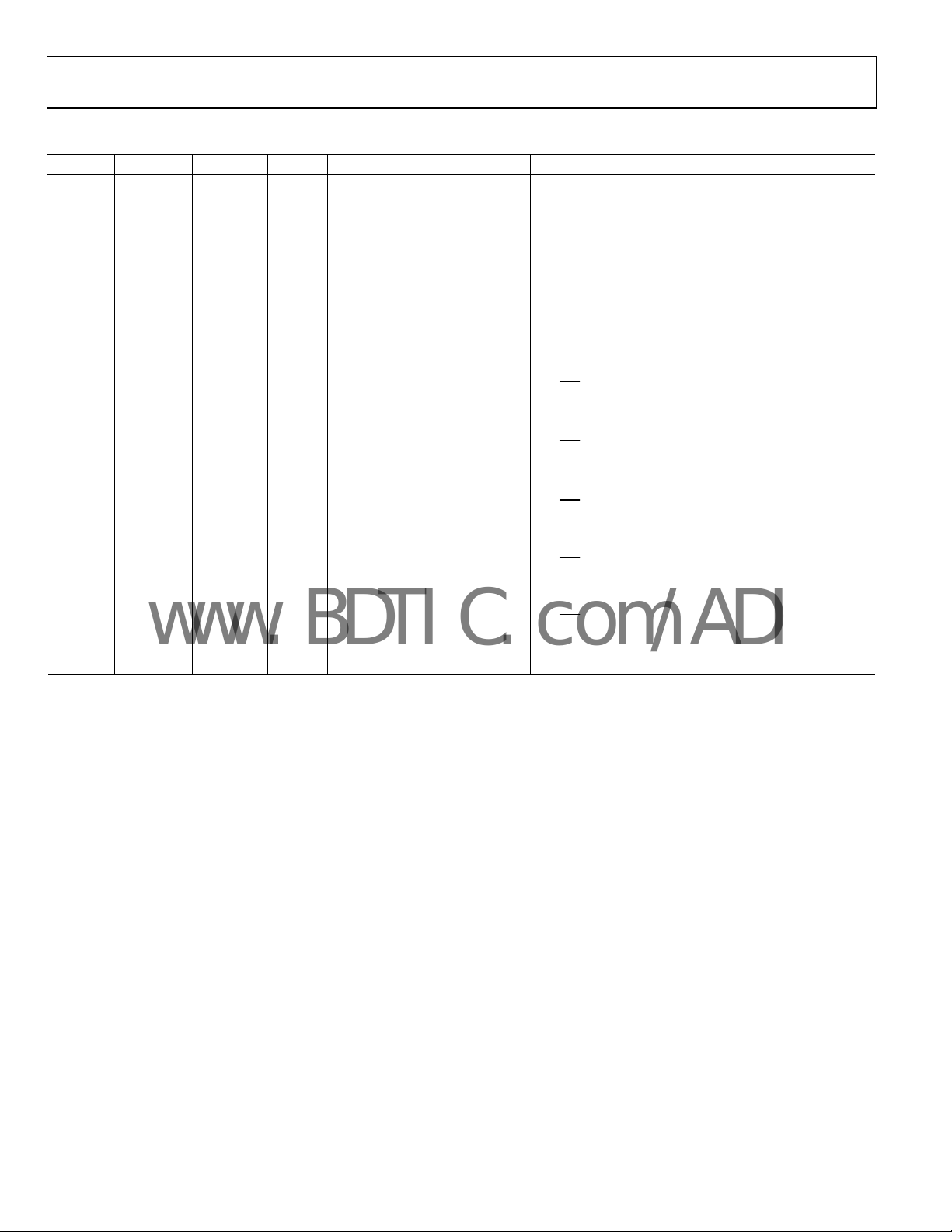
AD7143
www.BDTIC.com/ADI
Table 21. STAGE_LOW_INT_EN Register
Address Data Bit Default Type Name Description
0x005
[0] 0 STAGE0_LOW_INT_EN
[1] 0 STAGE1_LOW_INT_EN
R/W
STAGE0 low interrupt enable
terrupt source disabled
0 = in
asserted if STAGE0 low threshold is exceeded
1 = INT
STAGE1 low interrupt enable
terrupt source disabled
0 = in
asserted if STAGE0 low threshold is exceeded
1 = INT
[2] 0 STAGE2_LOW_INT_EN
[3] 0 STAGE3_LOW_INT_EN
[4] 0 STAGE4_LOW_INT_EN
[5] 0 STAGE5_LOW_INT_EN
[6] 0
[7] 0
[11:8] 0 Unused Set unused register bits = 0
[15:12] 0 TESTMODE Set test mode r
STAGE6_LOW_INT_EN
STAGE7_LOW_INT_EN
STAGE2 low interrupt enable
terrupt source disabled
0 = in
asserted if STAGE0 low threshold is exceeded
1 = INT
STAGE3 low interrupt enable
0 = in
terrupt source disabled
1 = INT
asserted if STAGE0 low threshold is exceeded
STAGE4 low interrupt enable
0 = in
terrupt source disabled
1 = INT
asserted if STAGE0 low threshold is exceeded
STAGE5 low interrupt enable
0 = in
terrupt source disabled
1 = INT
asserted if STAGE0 low threshold is exceeded
STAGE6 low interrupt enable
0 = in
terrupt source disabled
1 = INT
asserted if STAGE0 low threshold is exceeded
STAGE7 low interrupt enable
0 = in
terrupt source disabled
1 = INT
asserted if STAGE0 low threshold is exceeded
egister bits = 0 (at all times)
Rev. 0 | Page 38 of 56
AD7143
www.BDTIC.com/ADI
Table 22. STAGE_HIGH_INT_EN Register
Address Data Bit Default Type Name Description
0x006
[0] 0 STAGE0_HIGH_INT_EN
[1] 0 STAGE1_HIGH_INT_EN
[2] 0 STAGE2_HIGH_INT_EN
[3] 0 STAGE3_HIGH_INT_EN
[4] 0 STAGE4_HIGH_INT_EN
[5] 0 STAGE5_HIGH_INT_EN
[6] 0 STAGE6_HIGH_INT_EN
[7] 0 STAGE7_HIGH_INT_EN
[15:8]
R/W
Unused Set unused register bits = 0
STAGE0 high interrupt enable
terrupt source disabled
0 = in
asserted if STAGE0 high threshold is exceeded
1 = INT
STAGE1 high interrupt enable
terrupt source disabled
0 = in
asserted if STAGE0 high threshold is exceeded
1 = INT
STAGE2 high interrupt enable
terrupt source disabled
0 = in
asserted if STAGE0 high threshold is exceeded
1 = INT
STAGE3 high interrupt enable
0 = interrupt source disabled
1 = INT
asserted if STAGE0 high threshold is exceeded
STAGE4 high interrupt enable
0 = in
terrupt source disabled
1 = INT
asserted if STAGE0 high threshold is exceeded
STAGE5 high interrupt enable
0 = interrupt source disabled
1 = INT asserted if STAGE0 high threshold is exceeded
STAGE6 high interrupt enable
0 = interrupt source disabled
1 = INT asserted if STAGE0 high threshold is exceeded
STAGE7 high interrupt enable
0 = interrupt source disabled
1 = INT asserted if STAGE0 high threshold is exceeded
Rev. 0 | Page 39 of 56
AD7143
www.BDTIC.com/ADI
Table 23. STAGE_COMPLETE_INT_EN Register
Address Data Bit Default Type Name Description
0x007 [0] 0 R/W STAGE0_COMPLETE_EN STAGE0 conversion interrupt control
0 = interrupt source disabled
[1] 0 STAGE1_COMPLETE_EN STAGE1 conversion interrupt control
0 = interrupt source disabled
[2] 0 STAGE2_COMPLETE_EN STAGE2 conversion interrupt control
0 = interrupt source disabled
[3] 0 STAGE3_COMPLETE_EN STAGE3 conversion interrupt control
0 = interrupt source disabled
[4] 0 STAGE4_COMPLETE_EN STAGE4 conversion interrupt control
0 = interrupt source disabled
[5] 0 STAGE5_COMPLETE_EN STAGE5 conversion interrupt control
0 = interrupt source disabled
[6] 0 STAGE6_COMPLETE_EN STAGE6 conversion interrupt control
0 = interrupt source disabled
[7] 0 STAGE7_COMPLETE_EN STAGE7 conversion interrupt control
0 = interrupt source disabled
[11:8] 0 Unused Set unused register bits = 0
[12] 0 TESTMODE Set test mode register bits = 0 at all times
[15:13] Unused Set unused register bits = 0
asserted at completion of STAGE0 conversion
1 = INT
asserted at completion of STAGE1 conversion
1 = INT
asserted at completion of STAGE2 conversion
1 = INT
asserted at completion of STAGE3 conversion
1 = INT
asserted at completion of STAGE4 conversion
1 = INT
asserted at completion of STAGE5 conversion
1 = INT
asserted at completion of STAGE6 conversion
1 = INT
asserted at completion of STAGE7 conversion
1 = INT
Table 24. STAGE_LOW_LIMIT_INT Register
Address Data Bit Default Type Name Description
0x008 [0] 0 R STAGE0_LOW_LIMIT_INT STAGE0 CDC conversion low limit interrupt result
1 indicates STAGE0_LOW_THRESHOLD value exceeded
[1] 0 STAGE1_LOW_LIMIT_INT STAGE1 CDC conversion low limit interrupt result
1 indicates STAGE1_LOW_THRESHOLD value exceeded
[2] 0 STAGE2_LOW_LIMIT_INT STAGE2 CDC conversion low limit interrupt result
1 indicates STAGE2_LOW_THRESHOLD value exceeded
[3] 0 STAGE3_LOW_LIMIT_INT STAGE3 CDC conversion low limit interrupt result
1 indicates STAGE3_LOW_THRESHOLD value exceeded
[4] 0 STAGE4_LOW_LIMIT_INT STAGE4 CDC conversion low limit interrupt result
1 indicates STAGE4_LOW_THRESHOLD value exceeded
[5] 0 STAGE5_LOW_LIMIT_INT STAGE5 CDC conversion low limit interrupt result
1 indicates STAGE5_LOW_THRESHOLD value exceeded
[6] 0 STAGE6_LOW_LIMIT_INT STAGE6 CDC conversion low limit interrupt result
1 indicates STAGE6_LOW_THRESHOLD value exceeded
[7] 0 STAGE7_LOW_LIMIT_INT STAGE7 CDC conversion low limit interrupt result
1 indicates STAGE7_LOW_THRESHOLD value exceeded
[15:8] Unused Set unused register bits = 0
1
Registers self-clear to 0 after readback, provided that the limits are not exceeded.
1
Rev. 0 | Page 40 of 56
AD7143
www.BDTIC.com/ADI
Table 25. STAGE_HIGH_LIMIT_INT Register
Address Data Bit Default Type Name Description
0x009 [0] 0 R STAGE0_HIGH_LIMIT_INT STAGE0 CDC conversion high limit interrupt result
1 indicates STAGE0_HIGH_THRESHOLD value exceeded
[1] 0 STAGE1_HIGH_LIMIT_INT STAGE1 CDC conversion high limit interrupt result
1 indicates STAGE1_HIGH_THRESHOLD value exceeded
[2] 0 STAGE2_HIGH_LIMIT_INT Stage2 CDC conversion high limit interrupt result
1 indicates STAGE2_HIGH_THRESHOLD value exceeded
[3] 0 STAGE3_HIGH_LIMIT_INT STAGE3 CDC conversion high limit interrupt result
1 indicates STAGE3_HIGH_THRESHOLD value exceeded
[4] 0 STAGE4_HIGH_LIMIT_INT STAGE4 CDC conversion high limit interrupt result
1 indicates STAGE4_HIGH_THRESHOLD value exceeded
[5] 0 STAGE5_HIGH_LIMIT_INT STAGE5 CDC conversion high limit interrupt result
1 indicates STAGE5_HIGH_THRESHOLD value exceeded
[6] 0 STAGE6_HIGH_LIMIT_INT STAGE6 CDC conversion high limit interrupt result
1 indicates STAGE6_HIGH_THRESHOLD value exceeded
[7] 0 STAGE7_HIGH_LIMIT_INT STAGE7 CDC conversion high limit interrupt result
1 indicates STAGE7_HIGH_THRESHOLD value exceeded
[15:8] Unused Set unused register bits = 0
1
Registers self-clear to 0 after readback, provided that the limits are not exceeded.
1
Table 26. STAGE_COMPLETE_LIMIT_INT Register
Address Data Bit Default Type Name Description
0x00A [0] 0 R STAGE0_COMPLETE_STATUS_INT STAGE0 conversion complete register interrupt status
1 indicates STAGE0 conversion completed
[1] 0 STAGE1_COMPLETE_STATUS_INT STAGE1 conversion complete register interrupt status
1 indicates STAGE0 conversion completed
[2] 0 STAGE2_COMPLETE_STATUS_INT STAGE2 conversion complete register interrupt status
1 indicates STAGE0 conversion completed
[3] 0 STAGE3_COMPLETE_STATUS_INT STAGE3 conversion complete register interrupt status
1 indicates STAGE0 conversion completed
[4] 0 STAGE4_COMPLETE_STATUS_INT STAGE4 conversion complete register interrupt status
1 indicates STAGE0 conversion completed
[5] 0 STAGE5_COMPLETE_STATUS_INT STAGE5 conversion complete register interrupt status
1 indicates STAGE0 conversion completed
[6] 0 STAGE6_COMPLETE_STATUS_INT STAGE6 conversion complete register interrupt status
1 indicates STAGE0 conversion completed
[7] 0 STAGE7_COMPLETE_STATUS_INT STAGE7 conversion complete register interrupt status
1 indicates STAGE0 conversion completed
[15:8] 0 Unused
1
Registers self-clear to 0 after readback, provided that the limits are not exceeded.
1
Rev. 0 | Page 41 of 56

AD7143
www.BDTIC.com/ADI
Table 27. CDC 16-Bit Conversion Data Registers
Address Data Bit Default Type Name Description
0x00B [15:0] 0 R ADC_RESULT_S0 STAGE0 CDC 16-bit conversion data
0x00C [15:0] 0 R ADC_RESULT_S1 STAGE1 CDC 16-bit conversion data
0x00D [15:0] 0 R ADC_RESULT_S2 STAGE2 CDC 16-bit conversion data
0x00E [15:0] 0 R ADC_RESULT_S3 STAGE3 CDC 16-bit conversion data
0x00F [15:0] 0 R ADC_RESULT_S4 STAGE4 CDC 16-bit conversion data
0x010 [15:0] 0 R ADC_RESULT_S5 STAGE5 CDC 16-bit conversion data
0x011 [15:0] 0 R ADC_RESULT_S6 STAGE6 CDC 16-bit conversion data
0x012 [15:0] 0 R ADC_RESULT_S7 STAGE7 CDC 16-bit conversion data
Table 28. Device ID Register
Address Data Bit Default Type Name Description
0x017 [3:0] 0 R REVISION_CODE AD7143 revision code
[15:4] E63 DEVID AD7143 device ID = 0xE63
Table 29. Proximity Status Register
Address Data Bit Default Type Name Description
0x042 [0] 0 R STAGE0_PROXIMITY_STATUS STAGE0 proximity status register
1 indicates proximity detected on STAGE0
[1] 0 R STAGE1_PROXIMITY_STATUS STAGE1 proximity status register
1 indicates proximity detected on STAGE1
[2] 0 R STAGE2_PROXIMITY_STATUS STAGE2 proximity status register
1 indicates proximity detected on STAGE2
[3] 0 R STAGE3_PROXIMITY_STATUS STAGE3 proximity status register
1 indicates proximity detected on STAGE3
[4] 0 R STAGE4_PROXIMITY_STATUS STAGE4 proximity status register
1 indicates proximity detected on STAGE4
[5] 0 R STAGE5_PROXIMITY_STATUS STAGE5 proximity status register
1 indicates proximity detected on STAGE5
[6] 0 R STAGE6_PROXIMITY_STATUS STAGE6 proximity status register
1 indicates proximity detected on STAGE6
[7] 0 R STAGE7_PROXIMITY_STATUS STAGE7 proximity status register
1 indicates proximity detected on STAGE7
[15:8] Unused Set unused register bits = 0
Rev. 0 | Page 42 of 56
AD7143
www.BDTIC.com/ADI
BANK 2 REGISTERS
All address values are expressed in hexadecimal format.
Table 30. STAGE0 Configuration Registers
Address Data Bit Default Type Name Description
0x080 [15:0] X R/W STAGE0_CONNECTION[6:0] STAGE0 CIN(6:0) connection setup (see Table 38)
0x081 [15:0] X R/W STAGE0_CONNECTION 7 STAGE0 CIN7 connection setup (see Tab le 39)
0x082 [15:0] X R/W STAGE0_AFE_OFFSET STAGE0 AFE offset control (see Table 40)
0x083 [15:0] X R/W STAGE0_SENSITIVITY STAGE0 sensitivity control (see Table 4 1)
0x084 [15:0] X R/W STAGE0_OFFSET_LOW STAGE0 initial offset low value
0x085 [15:0] X R/W STAGE0_OFFSET_HIGH STAGE0 initial offset high value
0x086 [15:0] X R/W STAGE0_OFFSET_HIGH_CLAMP STAGE0 offset high clamp value
0x087 [15:0] X R/W STAGE0_OFFSET_LOW_CLAMP STAGE0 offset low clamp value
Table 31. STAGE1 Configuration Registers
Address Data Bit Default Type Name Description
0x088 [15:0] X R/W STAGE1_CONNECTION[6:0] STAGE1 CIN(6:0) connection setup (see Table 38)
0x089 [15:0] X R/W STAGE1_CONNECTION 7 STAGE1 CIN7 connection setup (see Tab l e 39)
0x08A [15:0] X R/W STAGE1_AFE_OFFSET STAGE1 AFE offset control (see Table 40)
0x08B [15:0] X R/W STAGE1_SENSITIVITY STAGE1 sensitivity control (see Tab le 41)
0x08C [15:0] X R/W STAGE1_OFFSET_LOW STAGE1 initial offset low value
0x08D [15:0] X R/W STAGE1_OFFSET_HIGH STAGE1 initial offset high value
0x08E [15:0] X R/W STAGE1_OFFSET_HIGH_CLAMP STAGE1 offset high clamp value
0x08F [15:0] X R/W STAGE1_OFFSET_LOW_CLAMP STAGE1 offset low clamp value
Table 32. STAGE2 Configuration Registers
Address Data Bit Default Type Name Description
0x090 [15:0] X R/W STAGE2_CONNECTION[6:0] STAGE2 CIN(6:0) connection setup (see Table 3 8 )
0x091 [15:0] X R/W STAGE2_CONNECTION 7 STAGE2 CIN7 connection setup (see Table 3 9)
0x092 [15:0] X R/W STAGE2_AFE_OFFSET STAGE2 AFE offset control (see Table 40)
0x093 [15:0] X R/W STAGE2_SENSITIVITY STAGE2 sensitivity control (see Tabl e 41)
0x094 [15:0] X R/W STAGE2_OFFSET_LOW STAGE2 initial offset low value
0x095 [15:0] X R/W STAGE2_OFFSET_HIGH STAGE2 initial offset high value
0x096 [15:0] X R/W STAGE2_OFFSET_HIGH_CLAMP STAGE2 offset high clamp value
0x097 [15:0] X R/W STAGE2_OFFSET_LOW_CLAMP STAGE2 offset low clamp value
Rev. 0 | Page 43 of 56

AD7143
www.BDTIC.com/ADI
Table 33. STAGE3 Configuration Registers
Address Data Bit Default Type Name Description
0x098 [15:0] X R/W STAGE3_CONNECTION[6:0] STAGE3 CIN(6:0) connection setup (see Table 38)
0x099 [15:0] X R/W STAGE3_CONNECTION 7 STAGE3 CIN7 connection setup (see Tabl e 39)
0x09A [15:0] X R/W STAGE3_AFE_OFFSET STAGE3 AFE offset control (see Table 40)
0x09B [15:0] X R/W STAGE3_SENSITIVITY STAGE3 sensitivity control (see Table 41)
0x09C [15:0] X R/W STAGE3_OFFSET_LOW STAGE3 initial offset low value
0x09D [15:0] X R/W STAGE3_OFFSET_HIGH STAGE3 initial offset high value
0x09E [15:0] X R/W STAGE3_OFFSET_HIGH_CLAMP STAGE3 offset high clamp value
0x09F [15:0] X R/W STAGE3_OFFSET_LOW_CLAMP STAGE3 offset low clamp value
Table 34. STAGE4 Configuration Registers
Address Data Bit Default Type Name Description
0x0A0 [15:0] X R/W STAGE4_CONNECTION[6:0] STAGE4 CIN(6:0) connection setup (see Table 3 8 )
0x0A1 [15:0] X R/W STAGE4_CONNECTION 7 STAGE4 CIN7 connection setup (see Table 39)
0x0A2 [15:0] X R/W STAGE4_AFE_OFFSET STAGE4 AFE offset control (see Table 40)
0x0A3 [15:0] X R/W STAGE4_SENSITIVITY STAGE4 sensitivity control (see Table 41)
0x0A4 [15:0] X R/W STAGE4_OFFSET_LOW STAGE4 initial offset low value
0x0A5 [15:0] X R/W STAGE4_OFFSET_HIGH STAGE4 initial offset high value
0x0A6 [15:0] X R/W STAGE4_OFFSET_HIGH_CLAMP STAGE4 offset high clamp value
0x0A7 [15:0] X R/W STAGE4_OFFSET_LOW_CLAMP STAGE4 offset low clamp value
Table 35. STAGE5 Configuration Registers
Address Data Bit Default Type Name Description
0x0A8 [15:0] X R/W STAGE5_CONNECTION[6:0] STAGE5 CIN(6:0) connection setup (see Table 3 8 )
0x0A9 [15:0] X R/W STAGE5_CONNECTION 7 STAGE5 CIN7 connection setup (see Table 39)
0x0AA [15:0] X R/W STAGE5_AFE_OFFSET STAGE5 AFE offset control (see Table 40)
0x0AB [15:0] X R/W STAGE5_SENSITIVITY STAGE5 sensitivity control (see Table 41)
0x0AC [15:0] X R/W STAGE5_OFFSET_LOW STAGE5 initial offset low value
0x0AD [15:0] X R/W STAGE5_OFFSET_HIGH STAGE5 initial offset high value
0x0AE [15:0] X R/W STAGE5_OFFSET_HIGH_CLAMP STAGE5 offset high clamp value
0x0AF [15:0] X R/W STAGE5_OFFSET_LOW_CLAMP STAGE5 offset low clamp value
Table 36. STAGE6 Configuration Registers
Address Data Bit Default Type Name Description
0x0B0 [15:0] X R/W STAGE6_CONNECTION[6:0] STAGE6 CIN(6:0) connection setup (see Table 3 8 )
0x0B1 [15:0] X R/W STAGE6_CONNECTION 7 STAGE6 CIN7 connection setup (see Table 39 )
0x0B2 [15:0] X R/W STAGE6_AFE_OFFSET STAGE6 AFE offset control (see Table 40 )
0x0B3 [15:0] X R/W STAGE6_SENSITIVITY STAGE6 sensitivity control (see Tabl e 41)
0x0B4 [15:0] X R/W STAGE6_OFFSET_LOW STAGE6 initial offset low value
0x0B5 [15:0] X R/W STAGE6_OFFSET_HIGH STAGE6 initial offset high value
0x0B6 [15:0] X R/W STAGE6_OFFSET_HIGH_CLAMP STAGE6 offset high clamp value
0x0B7 [15:0] X R/W STAGE6_OFFSET_LOW_CLAMP STAGE6 offset low clamp value
Rev. 0 | Page 44 of 56

AD7143
www.BDTIC.com/ADI
Table 37. STAGE7 Configuration Registers
Address Data Bit Default Type Name Description
0x0B8 [15:0] X R/W STAGE7_CONNECTION[6:0] STAGE7 CIN(6:0) connection setup (see Table 3 8 )
0x0B9 [15:0] X R/W STAGE7_CONNECTION 7 STAGE7 CIN7 connection setup (see Table 39 )
0x0BA [15:0] X R/W STAGE7_AFE_OFFSET STAGE7 AFE offset control (see Table 40)
0x0BB [15:0] X R/W STAGE7_SENSITIVITY STAGE7 sensitivity control (see Table 41)
0x0BC [15:0] X R/W STAGE7_OFFSET_LOW STAGE7 initial offset low value
0x0BD [15:0] X R/W STAGE7_OFFSET_HIGH STAGE7 initial offset high value
0x0BE [15:0] X R/W STAGE7_OFFSET_HIGH_CLAMP STAGE7 offset high clamp value
0x0BF [15:0] X R/W STAGE7_OFFSET_LOW_CLAMP STAGE7 offset low clamp value
Table 38. STAGEX Detailed CIN (0:6) Connection Setup Description (X = 0 to 6)
Data Bit Default Type Name Description
[1:0] X R/W CIN0_CONNECTION_SETUP CIN0 connection setup
00 = CIN0 not connected to CDC inputs
01 = CIN0 connected to CDC negative input
10 = CIN0 connected to CDC positive input
11 = CIN0 connected to BIAS (connect unused CIN inputs)
[3:2] X R/W CIN1_CONNECTION_SETUP CIN1 connection setup
00 = CIN1 not connected to CDC inputs
01 = CIN1 connected to CDC negative input
10 = CIN1 connected to CDC positive input
11 = CIN1 connected to BIAS (connect unused CIN inputs)
[5:4] X R/W CIN2_CONNECTION_SETUP CIN2 connection setup
00 = CIN2 not connected to CDC inputs
01 = CIN2 connected to CDC negative input
10 = CIN2 connected to CDC positive input
11 = CIN2 connected to BIAS (connect unused CIN inputs)
[7:6] X R/W CIN3_CONNECTION_SETUP CIN3 connection setup
00 = CIN3 not connected to CDC inputs
01 = CIN3 connected to CDC negative input
10 = CIN3 connected to CDC positive input
11 = CIN3 connected to BIAS (connect unused CIN inputs)
[9:8] X R/W CIN4_CONNECTION_SETUP CIN4 connection setup
00 = CIN4 not connected to CDC inputs
01 = CIN4 connected to CDC negative input
10 = CIN4 connected to CDC positive input
11 = CIN4 connected to BIAS (connect unused CIN inputs)
[11:10] X R/W CIN5_CONNECTION_SETUP CIN5 connection setup
00 = CIN5 not connected to CDC inputs
01 = CIN5 connected to CDC negative input
10 = CIN5 connected to CDC positive input
11 = CIN5 connected to BIAS (connect unused CIN inputs)
[13:12] X R/W CIN6_CONNECTION_SETUP CIN6 connection setup
00 = CIN6 not connected to CDC inputs
01 = CIN6 connected to CDC negative input
10 = CIN6 connected to CDC positive input
11 = CIN6 connected to BIAS (connect unused CIN inputs)
[15:14] X Unused
Rev. 0 | Page 45 of 56

AD7143
www.BDTIC.com/ADI
Table 39. STAGEX Detailed CIN7 Connection Setup Description
Data Bit Default Type Name Description
[1:0] X R/W CIN7_CONNECTION_SETUP CIN7 connection setup
00 = CIN7 not connected to CDC inputs
01 = CIN7 connected to CDC negative input
10 = CIN7 connected to CDC positive input
11 = CIN7 connected to BIAS (connect unused CIN inputs)
[13:2] X R/W Unused
[14] X R/W NEG_AFE_OFFSET_DISABLE Negative AFE offset enable control
0 = enable
1 = disable
[15] X R/W POS_AFE_OFFSET_DISABLE Positive AFE offset enable control
0 = enable
1 = disable
Table 40. STAGEX Detailed Offset Control Description (X = 0 to 7)
Data Bit Default Type Name Description
[6:0] X R/W NEG_AFE_OFFSET Negative AFE offset setting (20 pF range)
1 LSB value = 0.16 pF of offset
[7] X R/W NEG_AFE_OFFSET_SWAP Negative AFE offset swap control
0 = NEG_AFE_OFFSET applied to CDC negative input
1 = NEG_AFE_OFFSET applied to CDC positive input
[14:8] X R/W POS_AFE_OFFSET Positive AFE offset setting (20 pF range)
1 LSB value = 0.16 pF of offset
[15] X R/W POS_AFE_OFFSET_SWAP Positive AFE offset swap control
0 = POS_AFE_OFFSET applied to CDC positive input
1 = POS_AFE_OFFSET applied to CDC negative input
Table 41. STAGEX Detailed Sensitivity Control Description (X = 0 to 7)
Data Bit Default Type Name Description
[3:0] X R/W NEG_THRESHOLD_SENSITIVITY Negative threshold sensitivity control
0000 = 25%, 0001 = 29.73%, 0010 = 34.40%, 0011 = 39.08%
0100 = 43.79%, 0101 = 48.47%, 0110 = 53.15%
0111 = 57.83%, 1000 = 62.51%, 1001 = 67.22%
1010 = 71.90%, 1011 = 76.58%, 1100 = 81.28%
1101 = 85.96%, 1110 = 90.64%, 1111 = 95.32%
[6:4] X R/W NEG_PEAK_DETECT Negative peak detect setting
000 = 40% level, 001 = 50% level, 010 = 60% level
011 = 70% level, 100 = 80% level, 101 = 90% level
[7] X R/W Unused
[11:8] X R/W POS_THRESHOLD_SENSITIVITY Positive threshold sensitivity control
0000 = 25%, 0001 = 29.73%, 0010 = 34.40%, 0011 = 39.08%
0100 = 43.79%, 0101 = 48.47%, 0110 = 53.15%
0111 = 57.83%, 1000 = 62.51%, 1001 = 67.22%
1010 = 71.90%, 1011 = 76.58%, 1100 = 81.28%
1101 = 85.96%, 1110 = 90.64%, 1111 = 95.32%
[14:12] X R/W POS_PEAK_DETECT Positive peak detect setting
000 = 40% level, 001 = 50% level, 010 = 60% level
011 = 70% level, 100 = 80% level, 101 = 90% level
[15] X R/W Unused
Rev. 0 | Page 46 of 56

AD7143
www.BDTIC.com/ADI
BANK 3 REGISTERS
All address values are expressed in hexadecimal format.
Table 42. STAGE0 Results Registers
Address Data Bit Default Type Name Description
0x0E0 [15:0] X R/W STAGE0_CONV_DATA
0x0E1 [15:0] X R/W STAGE0_FF_WORD0 STAGE0 fast FIFO WORD0
0x0E2 [15:0] X R/W STAGE0_FF_WORD1 STAGE0 fast FIFO WORD1
0x0E3 [15:0] X R/W STAGE0_FF_WORD2 STAGE0 fast FIFO WORD2
0x0E4 [15:0] X R/W STAGE0_FF_WORD3 STAGE0 fast FIFO WORD3
0x0E5 [15:0] X R/W STAGE0_FF_WORD4 STAGE0 fast FIFO WORD4
0x0E6 [15:0] X R/W STAGE0_FF_WORD5 STAGE0 fast FIFO WORD5
0x0E7 [15:0] X R/W STAGE0_FF_WORD6 STAGE0 fast FIFO WORD6
0x0E8 [15:0] X R/W STAGE0_FF_WORD7 STAGE0 fast FIFO WORD7
0x0E9 [15:0] X R/W STAGE0_SF_WORD0 STAGE0 slow FIFO WORD0
0x0EA [15:0] X R/W STAGE0_SF_WORD1 STAGE0 slow FIFO WORD1
0x0EB [15:0] X R/W STAGE0_SF_WORD2 STAGE0 slow FIFO WORD2
0x0EC [15:0] X R/W STAGE0_SF_WORD3 STAGE0 slow FIFO WORD3
0x0ED [15:0] X R/W STAGE0_SF_WORD4 STAGE0 slow FIFO WORD4
0x0EE [15:0] X R/W STAGE0_SF_WORD5 STAGE0 slow FIFO WORD5
0x0EF [15:0] X R/W STAGE0_SF_WORD6 STAGE0 slow FIFO WORD6
0x0F0 [15:0] X R/W STAGE0_SF_WORD7 STAGE0 slow FIFO WORD7
0x0F1 [15:0] X R/W STAGE0_SF_AMBIENT STAGE0 slow FIFO ambient value
0x0F2 [15:0] X R/W STAGE0_FF_AVG STAGE0 fast FIFO average value
0x0F3 [15:0] X R/W STAGE0_PEAK_DETECT_WORD0 STAGE0 peak FIFO WORD0 value
0x0F4 [15:0] X R/W STAGE0_PEAK_DETECT_WORD1 STAGE0 peak FIFO WORD1 value
0x0F5 [15:0] X R/W STAGE0_MAX_WORD0 STAGE0 maximum value FIFO WORD0
0x0F6 [15:0] X R/W STAGE0_MAX_WORD1 STAGE0 maximum value FIFO WORD1
0x0F7 [15:0] X R/W STAGE0_MAX_WORD2 STAGE0 maximum value FIFO WORD2
0x0F8 [15:0] X R/W STAGE0_MAX_WORD3 STAGE0 maximum value FIFO WORD3
0x0F9 [15:0] X R/W STAGE0_MAX_AVG STAGE0 average maximum FIFO value
0x0FA [15:0] X R/W STAGE0_HIGH_THRESHOLD STAGE0 high threshold value
0x0FB [15:0] X R/W STAGE0_MAX_TEMP STAGE0 temporary maximum value
0x0FC [15:0] X R/W STAGE0_MIN_WORD0 STAGE0 minimum value FIFO WORD0
0x0FD [15:0] X R/W STAGE0_MIN_WORD1 STAGE0 minimum value FIFO WORD1
0x0FE [15:0] X R/W STAGE0_MIN_WORD2 STAGE0 minimum value FIFO WORD2
0x0FF [15:0] X R/W STAGE0_MIN_WORD3 STAGE0 minimum value FIFO WORD3
0x100 [15:0] X R/W STAGE0_MIN_AVG STAGE0 average minimum FIFO value
0x101 [15:0] X R/W STAGE0_LOW_THRESHOLD STAGE0 low threshold value
0x102 [15:0] X R/W STAGE0_MIN_TEMP STAGE0 temporary minimum value
0x103 [15:0] X R/W Unused
STAGE0 CDC 16-bit conversion data
opy of data in STAGE0_CONV_DATA register)
(c
Rev. 0 | Page 47 of 56

AD7143
www.BDTIC.com/ADI
Table 43. STAGE1 Results Registers
Address Data Bit Default Type Name Description
0x104 [15:0] X R/W STAGE1_CONV_DATA
0x105 [15:0] X R/W STAGE1_FF_WORD0 STAGE1 fast FIFO WORD0
0x106 [15:0] X R/W STAGE1_FF_WORD1 STAGE1 fast FIFO WORD1
0x107 [15:0] X R/W STAGE1_FF_WORD2 STAGE1 fast FIFO WORD2
0x108 [15:0] X R/W STAGE1_FF_WORD3 STAGE1 fast FIFO WORD3
0x109 [15:0] X R/W STAGE1_FF_WORD4 STAGE1 fast FIFO WORD4
0x10A [15:0] X R/W STAGE1_FF_WORD5 STAGE1 fast FIFO WORD5
0x10B [15:0] X R/W STAGE1_FF_WORD6 STAGE1 fast FIFO WORD6
0x10C [15:0] X R/W STAGE1_FF_WORD7 STAGE1 fast FIFO WORD7
0x10D [15:0] X R/W STAGE1_SF_WORD0 STAGE1 slow FIFO WORD0
0x10E [15:0] X R/W STAGE1_SF_WORD1 STAGE1 slow FIFO WORD1
0x10F [15:0] X R/W STAGE1_SF_WORD2 STAGE1 slow FIFO WORD2
0x110 [15:0] X R/W STAGE1_SF_WORD3 STAGE1 slow FIFO WORD3
0x111 [15:0] X R/W STAGE1_SF_WORD4 STAGE1 slow FIFO WORD4
0x112 [15:0] X R/W STAGE1_SF_WORD5 STAGE1 slow FIFO WORD5
0x113 [15:0] X R/W STAGE1_SF_WORD6 STAGE1 slow FIFO WORD6
0x114 [15:0] X R/W STAGE1_SF_WORD7 STAGE1 slow FIFO WORD7
0x115 [15:0] X R/W STAGE1_SF_AMBIENT STAGE1 slow FIFO ambient value
0x116 [15:0] X R/W STAGE1_FF_AVG STAGE1 fast FIFO average value
0x117 [15:0] X R/W STAGE1_CDC_WORD0 STAGE1 CDC FIFO WORD0
0x118 [15:0] X R/W STAGE1_CDC_WORD1 STAGE1 CDC FIFO WORD1
0x119 [15:0] X R/W STAGE1_MAX_WORD0 STAGE1 maximum value FIFO WORD0
0x11A [15:0] X R/W STAGE1_MAX_WORD1 STAGE1 maximum value FIFO WORD1
0x11B [15:0] X R/W STAGE1_MAX_WORD2 STAGE1 maximum value FIFO WORD2
0x11C [15:0] X R/W STAGE1_MAX_WORD3 STAGE1 maximum value FIFO WORD3
0x11D [15:0] X R/W STAGE1_MAX_AVG STAGE1 average maximum FIFO value
0x11E [15:0] X R/W STAGE1_HIGH_THRESHOLD STAGE1 high threshold value
0x11F [15:0] X R/W STAGE1_MAX_TEMP STAGE1 temporary maximum value
0x120 [15:0] X R/W STAGE1_MIN_WORD0 STAGE1 minimum value FIFO WORD0
0x121 [15:0] X R/W STAGE1_MIN_WORD1 STAGE1 minimum value FIFO WORD1
0x122 [15:0] X R/W STAGE1_MIN_WORD2 STAGE1 minimum value FIFO WORD2
0x123 [15:0] X R/W STAGE1_MIN_WORD3 STAGE1 minimum value FIFO WORD3
0x124 [15:0] X R/W STAGE1_MIN_AVG STAGE1 average minimum FIFO value
0x125 [15:0] X R/W STAGE1_LOW_THRESHOLD STAGE1 low threshold value
0x126 [15:0] X R/W STAGE1_MIN_TEMP STAGE1 temporary minimum value
0x127 [15:0] X R/W Unused
STAGE1 CDC 16-bit conversion data
opy of data in STAGE1_CONV_DATA register)
(c
Rev. 0 | Page 48 of 56
AD7143
www.BDTIC.com/ADI
Table 44. STAGE2 Results Registers
Address Data Bit Default Type Name Description
0x128 [15:0] X R/W STAGE2_CONV_DATA
0x129 [15:0] X R/W STAGE2_FF_WORD0 STAGE2 fast FIFO WORD0
0x12A [15:0] X R/W STAGE2_FF_WORD1 STAGE2 fast FIFO WORD1
0x12B [15:0] X R/W STAGE2_FF_WORD2 STAGE2 fast FIFO WORD2
0x12C [15:0] X R/W STAGE2_FF_WORD3 STAGE2 fast FIFO WORD3
0x12D [15:0] X R/W STAGE2_FF_WORD4 STAGE2 fast FIFO WORD4
0x12E [15:0] X R/W STAGE2_FF_WORD5 STAGE2 fast FIFO WORD5
0x12F [15:0] X R/W STAGE2_FF_WORD6 STAGE2 fast FIFO WORD6
0x130 [15:0] X R/W STAGE2_FF_WORD7 STAGE2 fast FIFO WORD7
0x131 [15:0] X R/W STAGE2_SF_WORD0 STAGE2 slow FIFO WORD0
0x132 [15:0] X R/W STAGE2_SF_WORD1 STAGE2 slow FIFO WORD1
0x133 [15:0] X R/W STAGE2_SF_WORD2 STAGE2 slow FIFO WORD2
0x134 [15:0] X R/W STAGE2_SF_WORD3 STAGE2 slow FIFO WORD3
0x135 [15:0] X R/W STAGE2_SF_WORD4 STAGE2 slow FIFO WORD4
0x125 [15:0] X R/W STAGE2_SF_WORD5 STAGE2 slow FIFO WORD5
0x137 [15:0] X R/W STAGE2_SF_WORD6 STAGE2 slow FIFO WORD6
0x138 [15:0] X R/W STAGE2_SF_WORD7 STAGE2 slow FIFO WORD7
0x139 [15:0] X R/W STAGE2_SF_AMBIENT STAGE2 slow FIFO ambient value
0x13A [15:0] X R/W STAGE2_FF_AVG STAGE2 fast FIFO average value
0x13B [15:0] X R/W STAGE2_CDC_WORD0 STAGE2 CDC FIFO WORD0
0x13C [15:0] X R/W STAGE2_CDC_WORD1 STAGE2 CDC FIFO WORD1
0x13D [15:0] X R/W STAGE2_MAX_WORD0 STAGE2 maximum value FIFO WORD0
0x13E [15:0] X R/W STAGE2_MAX_WORD1 STAGE2 maximum value FIFO WORD1
0x13F [15:0] X R/W STAGE2_MAX_WORD2 STAGE2 maximum value FIFO WORD2
0x140 [15:0] X R/W STAGE2_MAX_WORD3 STAGE2 maximum value FIFO WORD3
0x141 [15:0] X R/W STAGE2_MAX_AVG STAGE2 average maximum FIFO value
0x142 [15:0] X R/W STAGE2_HIGH_THRESHOLD STAGE2 high threshold value
0x143 [15:0] X R/W STAGE2_MAX_TEMP STAGE2 temporary maximum value
0x144 [15:0] X R/W STAGE2_MIN_WORD0 STAGE2 minimum value FIFO WORD0
0x145 [15:0] X R/W STAGE2_MIN_WORD1 STAGE2 minimum value FIFO WORD1
0x146 [15:0] X R/W STAGE2_MIN_WORD2 STAGE2 minimum value FIFO WORD2
0x147 [15:0] X R/W STAGE2_MIN_WORD3 STAGE2 minimum value FIFO WORD3
0x148 [15:0] X R/W STAGE2_MIN_AVG STAGE2 average minimum FIFO value
0x149 [15:0] X R/W STAGE2_LOW_THRESHOLD STAGE2 low threshold value
0x14A [15:0] X R/W STAGE2_MIN_TEMP STAGE2 temporary minimum value
0x14B [15:0] X R/W Unused
STAGE2 CDC 16-bit conversion data
opy of data in STAGE2_CONV_DATA register)
(c
Rev. 0 | Page 49 of 56

AD7143
www.BDTIC.com/ADI
Table 45. STAGE3 Results Registers
Address Data Bit Default Type Name Description
0x14C [15:0] X R/W STAGE3_CONV_DATA
0x14D [15:0] X R/W STAGE3_FF_WORD0 STAGE3 fast FIFO WORD0
0x14E [15:0] X R/W STAGE3_FF_WORD1 STAGE3 fast FIFO WORD1
0x14F [15:0] X R/W STAGE3_FF_WORD2 STAGE3 fast FIFO WORD2
0x150 [15:0] X R/W STAGE3_FF_WORD3 STAGE3 fast FIFO WORD3
0x151 [15:0] X R/W STAGE3_FF_WORD4 STAGE3 fast FIFO WORD4
0x152 [15:0] X R/W STAGE3_FF_WORD5 STAGE3 fast FIFO WORD5
0x153 [15:0] X R/W STAGE3_FF_WORD6 STAGE3 fast FIFO WORD6
0x154 [15:0] X R/W STAGE3_FF_WORD7 STAGE3 fast FIFO WORD7
0x155 [15:0] X R/W STAGE3_SF_WORD0 STAGE3 slow FIFO WORD0
0x156 [15:0] X R/W STAGE3_SF_WORD1 STAGE3 slow FIFO WORD1
0x157 [15:0] X R/W STAGE3_SF_WORD2 STAGE3 slow FIFO WORD2
0x158 [15:0] X R/W STAGE3_SF_WORD3 STAGE3 slow FIFO WORD3
0x159 [15:0] X R/W STAGE3_SF_WORD4 STAGE3 slow FIFO WORD4
0x15A [15:0] X R/W STAGE3_SF_WORD5 STAGE3 slow FIFO WORD5
0x15B [15:0] X R/W STAGE3_SF_WORD6 STAGE3 slow FIFO WORD6
0x15C [15:0] X R/W STAGE3_SF_WORD7 STAGE3 slow FIFO WORD7
0x15D [15:0] X R/W STAGE3_SF_AMBIENT STAGE3 slow FIFO ambient value
0x15E [15:0] X R/W STAGE3_FF_AVG STAGE3 fast FIFO average value
0x15F [15:0] X R/W STAGE3_CDC_WORD0 STAGE3 CDC FIFO WORD0
0x160 [15:0] X R/W STAGE3_CDC_WORD1 STAGE3 CDC FIFO WORD1
0x161 [15:0] X R/W STAGE3_MAX_WORD0 STAGE3 maximum value FIFO WORD0
0x162 [15:0] X R/W STAGE3_MAX_WORD1 STAGE3 maximum value FIFO WORD1
0x163 [15:0] X R/W STAGE3_MAX_WORD2 STAGE3 maximum value FIFO WORD2
0x164 [15:0] X R/W STAGE3_MAX_WORD3 STAGE3 maximum value FIFO WORD3
0x165 [15:0] X R/W STAGE3_MAX_AVG STAGE3 average maximum FIFO value
0x166 [15:0] X R/W STAGE3_HIGH_THRESHOLD STAGE3 high threshold value
0x167 [15:0] X R/W STAGE3_MAX_TEMP STAGE3 temporary maximum value
0x168 [15:0] X R/W STAGE3_MIN_WORD0 STAGE3 minimum value FIFO WORD0
0x169 [15:0] X R/W STAGE3_MIN_WORD1 STAGE3 minimum value FIFO WORD1
0x16A [15:0] X R/W STAGE3_MIN_WORD2 STAGE3 minimum value FIFO WORD2
0x16B [15:0] X R/W STAGE3_MIN_WORD3 STAGE3 minimum value FIFO WORD3
0x16C [15:0] X R/W STAGE3_MIN_AVG STAGE3 average minimum FIFO value
0x16D [15:0] X R/W STAGE3_LOW_THRESHOLD STAGE3 low threshold value
0x16E [15:0] X R/W STAGE3_MIN_TEMP STAGE3 temporary minimum value
0x16F [15:0] X R/W Unused
STAGE3 CDC 16-bit conversion data
opy of data in STAGE3_CONV_DATA register)
(c
Rev. 0 | Page 50 of 56

AD7143
www.BDTIC.com/ADI
Table 46. STAGE4 Results Registers
Address Data Bit Default Type Name Description
0x170 [15:0] X R/W STAGE4_CONV_DATA
0x171 [15:0] X R/W STAGE4_FF_WORD0 STAGE4 fast FIFO WORD0
0x172 [15:0] X R/W STAGE4_FF_WORD1 STAGE4 fast FIFO WORD1
0x173 [15:0] X R/W STAGE4_FF_WORD2 STAGE4 fast FIFO WORD2
0x174 [15:0] X R/W STAGE4_FF_WORD3 STAGE4 fast FIFO WORD3
0x175 [15:0] X R/W STAGE4_FF_WORD4 STAGE4 fast FIFO WORD4
0x176 [15:0] X R/W STAGE4_FF_WORD5 STAGE4 fast FIFO WORD5
0x177 [15:0] X R/W STAGE4_FF_WORD6 STAGE4 fast FIFO WORD6
0x178 [15:0] X R/W STAGE4_FF_WORD7 STAGE4 fast FIFO WORD7
0x179 [15:0] X R/W STAGE4_SF_WORD0 STAGE4 slow FIFO WORD0
0x17A [15:0] X R/W STAGE4_SF_WORD1 STAGE4 slow FIFO WORD1
0x17B [15:0] X R/W STAGE4_SF_WORD2 STAGE4 slow FIFO WORD2
0x17C [15:0] X R/W STAGE4_SF_WORD3 STAGE4 slow FIFO WORD3
0x17D [15:0] X R/W STAGE4_SF_WORD4 STAGE4 slow FIFO WORD4
0x17E [15:0] X R/W STAGE4_SF_WORD5 STAGE4 slow FIFO WORD5
0x17F [15:0] X R/W STAGE4_SF_WORD6 STAGE4 slow FIFO WORD6
0x180 [15:0] X R/W STAGE4_SF_WORD7 STAGE4 slow FIFO WORD7
0x181 [15:0] X R/W STAGE4_SF_AMBIENT STAGE4 slow FIFO ambient value
0x182 [15:0] X R/W STAGE4_FF_AVG STAGE4 fast FIFO average value
0x183 [15:0] X R/W STAGE4_CDC_WORD0 STAGE4 CDC FIFO WORD0
0x184 [15:0] X R/W STAGE4_CDC_WORD1 STAGE4 CDC FIFO WORD1
0x185 [15:0] X R/W STAGE4_MAX_WORD0 STAGE4 maximum value FIFO WORD0
0x186 [15:0] X R/W STAGE4_MAX_WORD1 STAGE4 maximum value FIFO WORD1
0x187 [15:0] X R/W STAGE4_MAX_WORD2 STAGE4 maximum value FIFO WORD2
0x188 [15:0] X R/W STAGE4_MAX_WORD3 STAGE4 maximum value FIFO WORD3
0x189 [15:0] X R/W STAGE4_MAX_AVG STAGE4 average maximum FIFO value
0x18A [15:0] X R/W STAGE4_HIGH_THRESHOLD STAGE4 high threshold value
0x18B [15:0] X R/W STAGE4_MAX_TEMP STAGE4 temporary maximum value
0x18C [15:0] X R/W STAGE4_MIN_WORD0 STAGE4 minimum value FIFO WORD0
0x18D [15:0] X R/W STAGE4_MIN_WORD1 STAGE4 minimum value FIFO WORD1
0x18E [15:0] X R/W STAGE4_MIN_WORD2 STAGE4 minimum value FIFO WORD2
0x18F [15:0] X R/W STAGE4_MIN_WORD3 STAGE4 minimum value FIFO WORD3
0x190 [15:0] X R/W STAGE4_MIN_AVG STAGE4 average minimum FIFO value
0x191 [15:0] X R/W STAGE4_LOW_THRESHOLD STAGE4 low threshold value
0x192 [15:0] X R/W STAGE4_MIN_TEMP STAGE4 temporary minimum value
0x193 [15:0] X R/W Unused
STAGE4 CDC 16-bit conversion data
opy of data in STAGE4_CONV_DATA register)
(c
Rev. 0 | Page 51 of 56

AD7143
www.BDTIC.com/ADI
Table 47. STAGE5 Results Registers
Address Data Bit Default Type Name Description
0x194 [15:0] X R/W STAGE5_CONV_DATA
0x195 [15:0] X R/W STAGE5_FF_WORD0 STAGE5 fast FIFO WORD0
0x196 [15:0] X R/W STAGE5_FF_WORD1 STAGE5 fast FIFO WORD1
0x197 [15:0] X R/W STAGE5_FF_WORD2 STAGE5 fast FIFO WORD2
0x198 [15:0] X R/W STAGE5_FF_WORD3 STAGE5 fast FIFO WORD3
0x199 [15:0] X R/W STAGE5_FF_WORD4 STAGE5 fast FIFO WORD4
0x19A [15:0] X R/W STAGE5_FF_WORD5 STAGE5 fast FIFO WORD5
0x19B [15:0] X R/W STAGE5_FF_WORD6 STAGE5 fast FIFO WORD6
0x19C [15:0] X R/W STAGE5_FF_WORD7 STAGE5 fast FIFO WORD7
0x19D [15:0] X R/W STAGE5_SF_WORD0 STAGE5 slow FIFO WORD0
0x19E [15:0] X R/W STAGE5_SF_WORD1 STAGE5 slow FIFO WORD1
0x19F [15:0] X R/W STAGE5_SF_WORD2 STAGE5 slow FIFO WORD2
0x1A0 [15:0] X R/W STAGE5_SF_WORD3 STAGE5 slow FIFO WORD3
0x1A1 [15:0] X R/W STAGE5_SF_WORD4 STAGE5 slow FIFO WORD4
0x1A2 [15:0] X R/W STAGE5_SF_WORD5 STAGE5 slow FIFO WORD5
0x1A3 [15:0] X R/W STAGE5_SF_WORD6 STAGE5 slow FIFO WORD6
0x1A4 [15:0] X R/W STAGE5_SF_WORD7 STAGE5 slow FIFO WORD7
0x1A5 [15:0] X R/W STAGE5_SF_AMBIENT STAGE5 slow FIFO ambient value
0x1A6 [15:0] X R/W STAGE5_FF_AVG STAGE5 fast FIFO average value
0x1A7 [15:0] X R/W STAGE5_CDC_WORD0 STAGE5 CDC FIFO WORD0
0x1A8 [15:0] X R/W STAGE5_CDC_WORD1 STAGE5 CDC FIFO WORD1
0x1A9 [15:0] X R/W STAGE5_MAX_WORD0 STAGE5 maximum value FIFO WORD0
0x1AA [15:0] X R/W STAGE5_MAX_WORD1 STAGE5 maximum value FIFO WORD1
0x1AB [15:0] X R/W STAGE5_MAX_WORD2 STAGE5 maximum value FIFO WORD2
0x1AC [15:0] X R/W STAGE5_MAX_WORD3 STAGE5 maximum value FIFO WORD3
0x1AD [15:0] X R/W STAGE5_MAX_AVG STAGE5 average maximum FIFO value
0x1AE [15:0] X R/W STAGE5_HIGH_THRESHOLD STAGE5 high threshold value
0x1AF [15:0] X R/W STAGE5_MAX_TEMP STAGE5 temporary maximum value
0x1B0 [15:0] X R/W STAGE5_MIN_WORD0 STAGE5 minimum value FIFO WORD0
0x1B1 [15:0] X R/W STAGE5_MIN_WORD1 STAGE5 minimum value FIFO WORD1
0x1B2 [15:0] X R/W STAGE5_MIN_WORD2 STAGE5 minimum value FIFO WORD2
0x1B3 [15:0] X R/W STAGE5_MIN_WORD3 STAGE5 minimum value FIFO WORD3
0x1B4 [15:0] X R/W STAGE5_MIN_AVG STAGE5 average minimum FIFO value
0x1B5 [15:0] X R/W STAGE5_LOW_THRESHOLD STAGE5 low threshold value
0x1B6 [15:0] X R/W STAGE5_MIN_TEMP STAGE5 temporary minimum value
0x1B7 [15:0] X R/W Unused
STAGE5 CDC 16-bit conversion data
opy of data in STAGE5_CONV_DATA register)
(c
Rev. 0 | Page 52 of 56

AD7143
www.BDTIC.com/ADI
Table 48. STAGE6 Results Registers
Address Data Bit Default Type Name Description
0x1B8 [15:0] X R/W STAGE6_CONV_DATA
0x1B9 [15:0] X R/W STAGE6_FF_WORD0 STAGE6 fast FIFO WORD0
0x1BA [15:0] X R/W STAGE6_FF_WORD1 STAGE6 fast FIFO WORD1
0x1BB [15:0] X R/W STAGE6_FF_WORD2 STAGE6 fast FIFO WORD2
0x1BC [15:0] X R/W STAGE6_FF_WORD3 STAGE6 fast FIFO WORD3
0x1BD [15:0] X R/W STAGE6_FF_WORD4 STAGE6 fast FIFO WORD4
0x1BE [15:0] X R/W STAGE6_FF_WORD5 STAGE6 fast FIFO WORD5
0x1BF [15:0] X R/W STAGE6_FF_WORD6 STAGE6 fast FIFO WORD6
0x1C0 [15:0] X R/W STAGE6_FF_WORD7 STAGE6 fast FIFO WORD7
0x1C1 [15:0] X R/W STAGE6_SF_WORD0 STAGE6 slow FIFO WORD0
0x1C2 [15:0] X R/W STAGE6_SF_WORD1 STAGE6 slow FIFO WORD1
0x1C3 [15:0] X R/W STAGE6_SF_WORD2 STAGE6 slow FIFO WORD2
0x1C4 [15:0] X R/W STAGE6_SF_WORD3 STAGE6 slow FIFO WORD3
0x1C5 [15:0] X R/W STAGE6_SF_WORD4 STAGE6 slow FIFO WORD4
0x1C6 [15:0] X R/W STAGE6_SF_WORD5 STAGE6 slow FIFO WORD5
0x1C7 [15:0] X R/W STAGE6_SF_WORD6 STAGE6 slow FIFO WORD6
0x1C8 [15:0] X R/W STAGE6_SF_WORD7 STAGE6 slow FIFO WORD7
0x1C9 [15:0] X R/W STAGE6_SF_AMBIENT STAGE6 slow FIFO ambient value
0x1CA [15:0] X R/W STAGE6_FF_AVG STAGE6 fast FIFO average value
0x1CB [15:0] X R/W STAGE6_CDC_WORD0 STAGE0 CDC FIFO WORD0
0x1CC [15:0] X R/W STAGE6_CDC_WORD1 STAGE6 CDC FIFO WORD1
0x1CD [15:0] X R/W STAGE6_MAX_WORD0 STAGE6 maximum value FIFO WORD0
0x1CE [15:0] X R/W STAGE6_MAX_WORD1 STAGE6 maximum value FIFO WORD1
0x1CF [15:0] X R/W STAGE6_MAX_WORD2 STAGE6 maximum value FIFO WORD2
0x1D0 [15:0] X R/W STAGE6_MAX_WORD3 STAGE6 maximum value FIFO WORD3
0x1D1 [15:0] X R/W STAGE6_MAX_AVG STAGE6 average maximum FIFO value
0x1D2 [15:0] X R/W STAGE6_HIGH_THRESHOLD STAGE6 high threshold value
0x1D3 [15:0] X R/W STAGE6_MAX_TEMP STAGE6 temporary maximum value
0x1D4 [15:0] X R/W STAGE6_MIN_WORD0 STAGE6 minimum value FIFO WORD0
0x1D5 [15:0] X R/W STAGE6_MIN_WORD1 STAGE6 minimum value FIFO WORD1
0x1D6 [15:0] X R/W STAGE6_MIN_WORD2 STAGE6 minimum value FIFO WORD2
0x1D7 [15:0] X R/W STAGE6_MIN_WORD3 STAGE6 minimum value FIFO WORD3
0x1D8 [15:0] X R/W STAGE6_MIN_AVG STAGE6 average minimum FIFO value
0x1D9 [15:0] X R/W STAGE6_LOW_THRESHOLD STAGE6 low threshold value
0x1DA [15:0] X R/W STAGE6_MIN_TEMP STAGE6 temporary minimum value
0x1DB [15:0] X R/W Unused
STAGE6 CDC 16-bit conversion data
opy of data in STAGE6_CONV_DATA register)
(c
Rev. 0 | Page 53 of 56
AD7143
www.BDTIC.com/ADI
Table 49. STAGE7 Results Registers
Address Data Bit Default Type Name Description
0x1DC [15:0] X R/W STAGE7_CONV_DATA
0x1DD [15:0] X R/W STAGE7_FF_WORD0 STAGE7 fast FIFO WORD0
0x1DE [15:0] X R/W STAGE7_FF_WORD1 STAGE7 fast FIFO WORD1
0x1DF [15:0] X R/W STAGE7_FF_WORD2 STAGE7 fast FIFO WORD2
0x1E0 [15:0] X R/W STAGE7_FF_WORD3 STAGE7 fast FIFO WORD3
0x1E1 [15:0] X R/W STAGE7_FF_WORD4 STAGE7 fast FIFO WORD4
0x1E2 [15:0] X R/W STAGE7_FF_WORD5 STAGE7 fast FIFO WORD5
0x1E3 [15:0] X R/W STAGE7_FF_WORD6 STAGE7 fast FIFO WORD6
0x1E4 [15:0] X R/W STAGE7_FF_WORD7 STAGE7 fast FIFO WORD7
0x1E5 [15:0] X R/W STAGE7_SF_WORD0 STAGE7 slow FIFO WORD0
0x1E6 [15:0] X R/W STAGE7_SF_WORD1 STAGE7 slow FIFO WORD1
0x1E7 [15:0] X R/W STAGE7_SF_WORD2 STAGE7 slow FIFO WORD2
0x1E8 [15:0] X R/W STAGE7_SF_WORD3 STAGE7 slow FIFO WORD3
0x1E9 [15:0] X R/W STAGE7_SF_WORD4 STAGE7 slow FIFO WORD4
0x1EA [15:0] X R/W STAGE7_SF_WORD5 STAGE7 slow FIFO WORD5
0x1EB [15:0] X R/W STAGE7_SF_WORD6 STAGE7 slow FIFO WORD6
0x1EC [15:0] X R/W STAGE7_SF_WORD7 STAGE7 slow FIFO WORD7
0x1ED [15:0] X R/W STAGE7_SF_AMBIENT STAGE7 slow FIFO ambient value
0x1EE [15:0] X R/W STAGE7_FF_AVG STAGE7 fast FIFO average value
0x1EF [15:0] X R/W STAGE7_CDC_WORD0 STAGE7 CDC FIFO WORD0
0x1F0 [15:0] X R/W STAGE7_CDC_WORD1 STAGE7 CDC FIFO WORD1
0x1F1 [15:0] X R/W STAGE7_MAX_WORD0 STAGE7 maximum value FIFO WORD0
0x1F2 [15:0] X R/W STAGE7_MAX_WORD1 STAGE7 maximum value FIFO WORD1
0x1F3 [15:0] X R/W STAGE7_MAX_WORD2 STAGE7 maximum value FIFO WORD2
0x1F4 [15:0] X R/W STAGE7_MAX_WORD3 STAGE7 maximum value FIFO WORD3
0x1F5 [15:0] X R/W STAGE7_MAX_AVG STAGE7 average maximum FIFO value
0x1F6 [15:0] X R/W STAGE7_HIGH_THRESHOLD STAGE7 high threshold value
0x1F7 [15:0] X R/W STAGE7_MAX_TEMP STAGE7 temporary maximum value
0x1F8 [15:0] X R/W STAGE7_MIN_WORD0 STAGE7 minimum value FIFO WORD0
0x1F9 [15:0] X R/W STAGE7_MIN_WORD1 STAGE7 minimum value FIFO WORD1
0x1FA [15:0] X R/W STAGE7_MIN_WORD2 STAGE7 minimum value FIFO WORD2
0x1FB [15:0] X R/W STAGE7_MIN_WORD3 STAGE7 minimum value FIFO WORD3
0x1FC [15:0] X R/W STAGE7_MIN_AVG STAGE7 average minimum FIFO value
0x1FD [15:0] X R/W STAGE7_LOW_THRESHOLD STAGE7 low threshold value
0x1FE [15:0] X R/W STAGE7_MIN_TEMP STAGE7 temporary minimum value
0x1FF [15:0] X R/W Unused
STAGE7 CDC 16-bit conversion data
opy of data in STAGE7_CONV_DATA register)
(c
Rev. 0 | Page 54 of 56
AD7143
C
www.BDTIC.com/ADI
OUTLINE DIMENSIONS
0.50
0.40
INDI
SEATING
PIN 1
ATO R
1.00
0.85
0.80
PLANE
12° MAX
4.00
BSC SQ
TOP VIEW
0.30
0.23
0.18
3.75
BSC SQ
0.80 MAX
0.65 TYP
0.05 MAX
0.02 NOM
0.20 REF
0.60 MAX
12
0.65
BSC
9
1.95 BCS
COPLANARITY
0.08
13
EXPOSED
8
BOTTOM VIEW
PA D
0.30
1
16
4
5
P
N
I
D
N
I
2.65
2.50 SQ
2.35
0.25 MIN
1
R
A
O
T
C
I
COMPLIANTTOJEDEC STANDARDS MO-220-VGGC.
031006-A
Figure 48. 16-Lead Lead Frame Chip Scale Package [LFCSP_VQ]
× 4 mm Very Thin Quad
4 mm
(CP-16-13)
Dimensions shown in millimeters
ORDERING GUIDE
Model Temperature Range Serial Interface Description Package Description Package Option
AD7143ACPZ-1REEL
AD7143ACPZ-1500RL7
EVAL-AD7143-1EBZ
1
Z = Pb-free part.
1
1
−40°C to +85°C I2C Interface 16-Lead LFCSP_VQ CP-16-13
1
−40°C to +85°C I2C Interface 16-Lead LFCSP_VQ CP-16-13
I
2
C Interface Evaluation Board
Rev. 0 | Page 55 of 56
AD7143
www.BDTIC.com/ADI
NOTES
Purchase of licensed I2C components of Analog Devices or one of its sublicensed Associated Companies conveys a license for the purchaser under the Philips I2C Patent
Rights to use these components in an I
©2007 Analog Devices, Inc. All rights reserved. Trademarks and
registered trademarks are the property of their respective owners.
D06472-0-1/07(0)
2
C system, provided that the system conforms to the I2C Standard Specification as defined by Philips.
Rev. 0 | Page 56 of 56
 Loading...